

Page 1

EiceDRIVER™ 1ED38x0Mc12M Enhanced
1ED38x0Mc12M (1ED-X3 Digital)
Reference manual
Single-channel 5.7 kV (rms) isolated gate driver IC with I2C configurability for
DESAT, So-o, UVLO, Miller clamp and optional two-level turn-o
Features
• 650 V, 1200 V, 1700 V, 2300 V IGBTs, SiC, and Si MOSFETs
• 40 V absolute maximum output supply voltage
• ±3 A, ±6 A, and ±9 A typical sinking and sourcing peak output current
• Separate source and sink outputs for hard switching or optional two-level turn-o and with active Miller
clamp
• I2C bus for parameter configuration and status register readout
• Precise, adjustable, and temperature compensated V
• Adjustable IGBT so turn-o aer desaturation detection
• Operation at high ambient temperature up to 125 °C with over-temperature shut down at 160 °C (±10 °C)
• Tight IC-to-IC propagation delay matching (t
• Undervoltage lockout protection with hysteresis for input and output side with active shut-down
• Configurable feedback or fault-o behavior for comparator result of integrated ADC
• High common-mode transient immunity CMTI = 200 kV/µs
• Small space-saving DSO-16 fine-pitch package with large creepage distance (>8 mm)
• Safety certification
- UL 1577 recognized (File E311313) with V
- IEC 60747-17/VDE 0884-11 approval (pending) with V
• Refer to the product datasheet for electrical parameters and certification details
PDD,max
ISO,test
detection (DESAT) with fault output
CEsat
= 30 ns)
= 6840 V (rms) for 1 s, V
= 1767 V (peak, reinforced)
IORM
= 5700 V (rms) for 60 s
ISO
Potential applications
• Industrial motor drives - compact, standard, premium, servo drives
• Solar inverters
• UPS systems
• Welding
• Commercial and agricultural vehicles (CAV)
• Commercial air-conditioning (CAC)
• High-voltage isolated DC-DC converters
• Isolated switch mode power supplies (SMPS)
Product validation
Qualified for industrial applications according to the relevant tests of JEDEC47/20/22.
PG-DSO-16
Reference manual
www.infineon.com/gdisolated 2021-02-15
Please read the Important Notice and Warnings at the end of this document v2.1
Page 2
EiceDRIVER
™
1ED38x0Mc12M Enhanced
Reference manual
Device information
Device information
Product type Output current Isolation class Marking OPN
1ED3830MC12M 3 A (typ) reinforced 3830MC12 1ED3830MC12MXUMA1
1ED3860MC12M 6 A (typ) reinforced 3860MC12 1ED3860MC12MXUMA1
1ED3890MC12M 9 A (typ) reinforced 3890MC12 1ED3890MC12MXUMA1
1ED3830MU12M 3 A (typ) UL 1577 3830MU12 1ED3830MU12MXUMA1
1ED3860MU12M 6 A (typ) UL 1577 3860MU12 1ED3860MU12MXUMA1
1ED3890MU12M 9 A (typ) UL 1577 3890MU12 1ED3890MU12MXUMA1
Description
The 1ED38x0Mc12M family (X3 Digital) consists of galvanically isolated single channel gate driver ICs in a small
PG-DSO-16 package with a large creepage and clearance of 8 mm. The gate driver ICs provide a typical peak
output current of 3 A, 6 A, and 9 A.
Adjustable control and protection functions are included to simplify the design of highly reliable systems. All
parameter adjustments are done from the input side via the I2C interface (pin SDA and SCL).
All logic I/O pins are supply voltage dependent 3.3 V or 5 V CMOS compatible and can be directly connected to a
microcontroller.
The data transfer across the galvanic isolation is realized by the integrated coreless transformer technology.
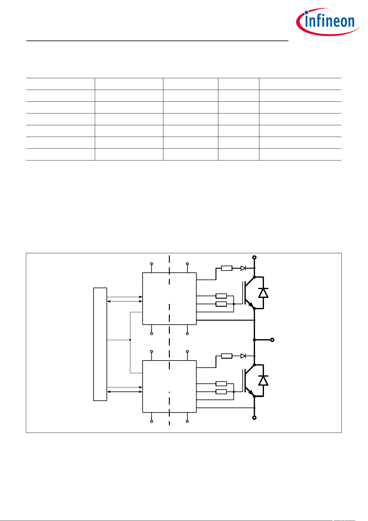
CPU
IN,H
RDYC, FLT_N
I2C
IN,L
RDYC, FLT_N
VCC1
GND1
VCC1
GND1
EiceDRIVER
with digital
interface
EiceDRIVER
with digital
interface
VCC2,H
DESAT,H
TM
ON,H
OFF,H
CLAMP,H
GND2,H
VEE2,H
VCC2,L
DESAT,L
TM
ON,L
OFF,L
CLAMP,L
GND2,L
VEE2,L
Figure 1 Typical application
Reference manual 2 v2.1
2021-02-15
Page 3

™
EiceDRIVER
1ED38x0Mc12M Enhanced
Reference manual
Table of contents
Table of contents
Table of contents . . . . . . . . . . . . . . . . . . . . . . . . . . . . . . . . . . . . . . . . . . . . . . . . . . . . . . . . . . . . . . . . . . . . . . . 3
1 Block diagram . . . . . . . . . . . . . . . . . . . . . . . . . . . . . . . . . . . . . . . . . . . . . . . . . . . . . . . . . . . . . . . . . . . . . . . . . . 6
2 Related products . . . . . . . . . . . . . . . . . . . . . . . . . . . . . . . . . . . . . . . . . . . . . . . . . . . . . . . . . . . . . . . . . . . . . . . 7
3 Functional description . . . . . . . . . . . . . . . . . . . . . . . . . . . . . . . . . . . . . . . . . . . . . . . . . . . . . . . . . . . . . . . . . .8
3.1 Start-up and fault clearing . . . . . . . . . . . . . . . . . . . . . . . . . . . . . . . . . . . . . . . . . . . . . . . . . . . . . . . . . . . . . . . .8
3.2 Supply . . . . . . . . . . . . . . . . . . . . . . . . . . . . . . . . . . . . . . . . . . . . . . . . . . . . . . . . . . . . . . . . . . . . . . . . . . . . . . . . . 9
3.2.1 Input side undervoltage lockout, VCC1 UVLO . . . . . . . . . . . . . . . . . . . . . . . . . . . . . . . . . . . . . . . . . . . . 10
3.2.2 Output side under-voltage lockout, VCC2 UVLO . . . . . . . . . . . . . . . . . . . . . . . . . . . . . . . . . . . . . . . . . . 11
3.2.3 Output side undervoltage lockout, VEE2 UVLO . . . . . . . . . . . . . . . . . . . . . . . . . . . . . . . . . . . . . . . . . . . 12
3.3 Input side logic . . . . . . . . . . . . . . . . . . . . . . . . . . . . . . . . . . . . . . . . . . . . . . . . . . . . . . . . . . . . . . . . . . . . . . . . .13
3.3.1 IN non-inverting driver input . . . . . . . . . . . . . . . . . . . . . . . . . . . . . . . . . . . . . . . . . . . . . . . . . . . . . . . . . . .13
3.3.2 RDYC ready status output, fault-o and fault clear input . . . . . . . . . . . . . . . . . . . . . . . . . . . . . . . . . . 13
3.3.2.1 Ready sources and configuration of not ready events . . . . . . . . . . . . . . . . . . . . . . . . . . . . . . . . . . 13
3.3.2.2 RDYC fault-o input . . . . . . . . . . . . . . . . . . . . . . . . . . . . . . . . . . . . . . . . . . . . . . . . . . . . . . . . . . . . . . . . . 14
3.3.2.3 RDYC fault clear input . . . . . . . . . . . . . . . . . . . . . . . . . . . . . . . . . . . . . . . . . . . . . . . . . . . . . . . . . . . . . . . 14
3.3.3 FLT_N status output and fault-o input . . . . . . . . . . . . . . . . . . . . . . . . . . . . . . . . . . . . . . . . . . . . . . . . . .15
3.3.3.1 Fault sources and configuration of fault events . . . . . . . . . . . . . . . . . . . . . . . . . . . . . . . . . . . . . . . . 15
3.3.3.2 FLT_N fault-o input . . . . . . . . . . . . . . . . . . . . . . . . . . . . . . . . . . . . . . . . . . . . . . . . . . . . . . . . . . . . . . . . 16
3.3.4 I2C bus . . . . . . . . . . . . . . . . . . . . . . . . . . . . . . . . . . . . . . . . . . . . . . . . . . . . . . . . . . . . . . . . . . . . . . . . . . . . . . 16
3.3.4.1 I2C bus byte format . . . . . . . . . . . . . . . . . . . . . . . . . . . . . . . . . . . . . . . . . . . . . . . . . . . . . . . . . . . . . . . . .17
3.3.4.2 I2C bus read/write operation . . . . . . . . . . . . . . . . . . . . . . . . . . . . . . . . . . . . . . . . . . . . . . . . . . . . . . . . 18
3.3.4.3 I2C bus address . . . . . . . . . . . . . . . . . . . . . . . . . . . . . . . . . . . . . . . . . . . . . . . . . . . . . . . . . . . . . . . . . . . . 19
3.4 Operating states . . . . . . . . . . . . . . . . . . . . . . . . . . . . . . . . . . . . . . . . . . . . . . . . . . . . . . . . . . . . . . . . . . . . . . . .21
3.4.1 OFF state . . . . . . . . . . . . . . . . . . . . . . . . . . . . . . . . . . . . . . . . . . . . . . . . . . . . . . . . . . . . . . . . . . . . . . . . . . . . 21
3.4.2 Address configuration state . . . . . . . . . . . . . . . . . . . . . . . . . . . . . . . . . . . . . . . . . . . . . . . . . . . . . . . . . . . .22
3.4.3 Parameter configuration state . . . . . . . . . . . . . . . . . . . . . . . . . . . . . . . . . . . . . . . . . . . . . . . . . . . . . . . . . .22
3.4.4 Parameter transfer state . . . . . . . . . . . . . . . . . . . . . . . . . . . . . . . . . . . . . . . . . . . . . . . . . . . . . . . . . . . . . . . 22
3.4.5 Normal operation state . . . . . . . . . . . . . . . . . . . . . . . . . . . . . . . . . . . . . . . . . . . . . . . . . . . . . . . . . . . . . . . .23
3.4.6 Not ready state . . . . . . . . . . . . . . . . . . . . . . . . . . . . . . . . . . . . . . . . . . . . . . . . . . . . . . . . . . . . . . . . . . . . . . . 23
3.4.7 Fault state . . . . . . . . . . . . . . . . . . . . . . . . . . . . . . . . . . . . . . . . . . . . . . . . . . . . . . . . . . . . . . . . . . . . . . . . . . . 23
3.4.8 So-reset, restore and recovery . . . . . . . . . . . . . . . . . . . . . . . . . . . . . . . . . . . . . . . . . . . . . . . . . . . . . . . .25
3.4.8.1 So-reset . . . . . . . . . . . . . . . . . . . . . . . . . . . . . . . . . . . . . . . . . . . . . . . . . . . . . . . . . . . . . . . . . . . . . . . . . .25
3.4.8.2 Automatic configuration restore from input side . . . . . . . . . . . . . . . . . . . . . . . . . . . . . . . . . . . . . . .25
3.4.8.3 Automatic configuration recovery from output side . . . . . . . . . . . . . . . . . . . . . . . . . . . . . . . . . . . .26
3.5 Measurement . . . . . . . . . . . . . . . . . . . . . . . . . . . . . . . . . . . . . . . . . . . . . . . . . . . . . . . . . . . . . . . . . . . . . . . . . . 27
3.6 Monitoring . . . . . . . . . . . . . . . . . . . . . . . . . . . . . . . . . . . . . . . . . . . . . . . . . . . . . . . . . . . . . . . . . . . . . . . . . . . . .27
3.7 Desaturation protection . . . . . . . . . . . . . . . . . . . . . . . . . . . . . . . . . . . . . . . . . . . . . . . . . . . . . . . . . . . . . . . . .29
3.7.1 DESAT behavior . . . . . . . . . . . . . . . . . . . . . . . . . . . . . . . . . . . . . . . . . . . . . . . . . . . . . . . . . . . . . . . . . . . . . . 29
3.7.2 DESAT adjustment . . . . . . . . . . . . . . . . . . . . . . . . . . . . . . . . . . . . . . . . . . . . . . . . . . . . . . . . . . . . . . . . . . . . 30
Reference manual 3 v2.1
2021-02-15
Page 4

™
EiceDRIVER
1ED38x0Mc12M Enhanced
Reference manual
Table of contents
3.7.2.1 DESAT1 adjustment . . . . . . . . . . . . . . . . . . . . . . . . . . . . . . . . . . . . . . . . . . . . . . . . . . . . . . . . . . . . . . . . .30
3.7.2.2 DESAT2 adjustment . . . . . . . . . . . . . . . . . . . . . . . . . . . . . . . . . . . . . . . . . . . . . . . . . . . . . . . . . . . . . . . . .30
3.8 Gate driver output . . . . . . . . . . . . . . . . . . . . . . . . . . . . . . . . . . . . . . . . . . . . . . . . . . . . . . . . . . . . . . . . . . . . . .32
3.8.1 Turn-on behavior . . . . . . . . . . . . . . . . . . . . . . . . . . . . . . . . . . . . . . . . . . . . . . . . . . . . . . . . . . . . . . . . . . . . .33
3.8.2 Turn-o and fault turn-o behavior . . . . . . . . . . . . . . . . . . . . . . . . . . . . . . . . . . . . . . . . . . . . . . . . . . . . .33
3.8.2.1 Hard switching turn-o . . . . . . . . . . . . . . . . . . . . . . . . . . . . . . . . . . . . . . . . . . . . . . . . . . . . . . . . . . . . . 34
3.8.2.2 Two-level turn-o . . . . . . . . . . . . . . . . . . . . . . . . . . . . . . . . . . . . . . . . . . . . . . . . . . . . . . . . . . . . . . . . . . 34
3.8.2.2.1 Two-level turn-o behavior at normal operating conditions . . . . . . . . . . . . . . . . . . . . . . . . . . 35
3.8.2.2.2 Two-level turn-o behavior at overload condition . . . . . . . . . . . . . . . . . . . . . . . . . . . . . . . . . . . 36
3.8.2.2.3 Two-level turn-o short pulse behavior . . . . . . . . . . . . . . . . . . . . . . . . . . . . . . . . . . . . . . . . . . . . 37
3.8.2.2.4 Two-level turn-o short pulse behavior with slow turn-on ramp speed . . . . . . . . . . . . . . . . 37
3.8.2.3 So turn-o . . . . . . . . . . . . . . . . . . . . . . . . . . . . . . . . . . . . . . . . . . . . . . . . . . . . . . . . . . . . . . . . . . . . . . . 38
3.8.2.4 Switch-o timeout until forced switch-o . . . . . . . . . . . . . . . . . . . . . . . . . . . . . . . . . . . . . . . . . . . . .38
3.8.3 Active shut-down . . . . . . . . . . . . . . . . . . . . . . . . . . . . . . . . . . . . . . . . . . . . . . . . . . . . . . . . . . . . . . . . . . . . . 39
3.8.4 Active Miller clamp . . . . . . . . . . . . . . . . . . . . . . . . . . . . . . . . . . . . . . . . . . . . . . . . . . . . . . . . . . . . . . . . . . . .39
3.8.4.1 CLAMP output types . . . . . . . . . . . . . . . . . . . . . . . . . . . . . . . . . . . . . . . . . . . . . . . . . . . . . . . . . . . . . . . . 39
3.9 Short circuit clamping . . . . . . . . . . . . . . . . . . . . . . . . . . . . . . . . . . . . . . . . . . . . . . . . . . . . . . . . . . . . . . . . . . 41
4 Register description . . . . . . . . . . . . . . . . . . . . . . . . . . . . . . . . . . . . . . . . . . . . . . . . . . . . . . . . . . . . . . . . . . . 42
4.1 Configuration registers . . . . . . . . . . . . . . . . . . . . . . . . . . . . . . . . . . . . . . . . . . . . . . . . . . . . . . . . . . . . . . . . . .44
4.1.1 I2CADD: I2C address of gate driver . . . . . . . . . . . . . . . . . . . . . . . . . . . . . . . . . . . . . . . . . . . . . . . . . . . . . .44
4.1.2 I2CGADD: I2C group address of gate driver . . . . . . . . . . . . . . . . . . . . . . . . . . . . . . . . . . . . . . . . . . . . . . 44
4.1.3 I2CCFGOK: I2C address configuration access . . . . . . . . . . . . . . . . . . . . . . . . . . . . . . . . . . . . . . . . . . . . .45
4.1.4 PSUPR: Input pin filter times for IN, RDYC, FLT_N, and I2C . . . . . . . . . . . . . . . . . . . . . . . . . . . . . . . . . 45
4.1.5 FCLR: FLT_N clear behavior by RDYC or timer . . . . . . . . . . . . . . . . . . . . . . . . . . . . . . . . . . . . . . . . . . . . 46
4.1.6 RECOVER: Input and output configuration recovery modes . . . . . . . . . . . . . . . . . . . . . . . . . . . . . . . 47
4.1.7 UVTLVL: UVLO threshold level for VCC2 and VEE2 . . . . . . . . . . . . . . . . . . . . . . . . . . . . . . . . . . . . . . . . . 48
4.1.8 UVSVCC2C: VCC2 so UVLO enable and threshold level . . . . . . . . . . . . . . . . . . . . . . . . . . . . . . . . . . . 49
4.1.9 UVSVEE2C: VEE2 so UVLO enable and threshold level . . . . . . . . . . . . . . . . . . . . . . . . . . . . . . . . . . . .50
4.1.10 ADCCFG: ADC enable and compare polarity . . . . . . . . . . . . . . . . . . . . . . . . . . . . . . . . . . . . . . . . . . . . . .51
4.1.11 VEXTCFG: CLAMP pin voltage compare limit . . . . . . . . . . . . . . . . . . . . . . . . . . . . . . . . . . . . . . . . . . . . . .53
4.1.12 OTWCFG: Over-temperature warning level and action . . . . . . . . . . . . . . . . . . . . . . . . . . . . . . . . . . . . 53
4.1.13 D1LVL: DESAT disable and DESAT1 voltage threshold level . . . . . . . . . . . . . . . . . . . . . . . . . . . . . . . . 54
4.1.14 D1FILT: DESAT1 filter time and type . . . . . . . . . . . . . . . . . . . . . . . . . . . . . . . . . . . . . . . . . . . . . . . . . . . . .55
4.1.15 D2LVL: DESAT2 enable during TLTO, influence on fault o, and voltage threshold level . . . . . 56
4.1.16 D2FILT: DESAT2 filter time and type . . . . . . . . . . . . . . . . . . . . . . . . . . . . . . . . . . . . . . . . . . . . . . . . . . . . .58
4.1.17 D2CNTLIM: DESAT2 event counter limit . . . . . . . . . . . . . . . . . . . . . . . . . . . . . . . . . . . . . . . . . . . . . . . . . 59
4.1.18 D2CNTDEC: DESAT2 event count down . . . . . . . . . . . . . . . . . . . . . . . . . . . . . . . . . . . . . . . . . . . . . . . . . .60
4.1.19 DLEBT: DESAT leading edge blanking time . . . . . . . . . . . . . . . . . . . . . . . . . . . . . . . . . . . . . . . . . . . . . . 61
4.1.20 F2ODLY: Delay from fault event to gate driver o . . . . . . . . . . . . . . . . . . . . . . . . . . . . . . . . . . . . . . . . . 62
4.1.21 DTECOR: DESAT temperature compensation . . . . . . . . . . . . . . . . . . . . . . . . . . . . . . . . . . . . . . . . . . . . .63
4.1.22 DRVFOFF: Type of fault switch-o . . . . . . . . . . . . . . . . . . . . . . . . . . . . . . . . . . . . . . . . . . . . . . . . . . . . . . 64
Reference manual 4 v2.1
2021-02-15
Page 5

™
EiceDRIVER
1ED38x0Mc12M Enhanced
Reference manual
Table of contents
4.1.23 DRVCFG: Type of normal switch-o and TLTO gate charge range . . . . . . . . . . . . . . . . . . . . . . . . . .65
4.1.24 TLTOC1: TLTO level and ramp A . . . . . . . . . . . . . . . . . . . . . . . . . . . . . . . . . . . . . . . . . . . . . . . . . . . . . . . 66
4.1.25 TLTOC2: TLTO duration and ramp B . . . . . . . . . . . . . . . . . . . . . . . . . . . . . . . . . . . . . . . . . . . . . . . . . . . .67
4.1.26 CSSOFCFG: So turn-o current . . . . . . . . . . . . . . . . . . . . . . . . . . . . . . . . . . . . . . . . . . . . . . . . . . . . . . . .68
4.1.27 CLCFG: CLAMP and pin monitoring filter time and type, CLAMP output types and disable . . . . . 68
4.1.28 SOTOUT: Switch-o timeout time and fault signaling . . . . . . . . . . . . . . . . . . . . . . . . . . . . . . . . . . . . .70
4.1.29 CFGOK: Register configuration lock . . . . . . . . . . . . . . . . . . . . . . . . . . . . . . . . . . . . . . . . . . . . . . . . . . . . . 71
4.1.30 CLEARREG: Clear event counter registers for DESAT2, VCC1 UVLO, VCC2 UVLO, event flags,
and so-reset . . . . . . . . . . . . . . . . . . . . . . . . . . . . . . . . . . . . . . . . . . . . . . . . . . . . . . . . . . . . . . . . . . . . . . . . 71
4.2 Status registers . . . . . . . . . . . . . . . . . . . . . . . . . . . . . . . . . . . . . . . . . . . . . . . . . . . . . . . . . . . . . . . . . . . . . . . . .73
4.2.1 Sticky bits . . . . . . . . . . . . . . . . . . . . . . . . . . . . . . . . . . . . . . . . . . . . . . . . . . . . . . . . . . . . . . . . . . . . . . . . . . . .73
4.2.2 RDYSTAT: Status of input side, output side, and gate driver IC . . . . . . . . . . . . . . . . . . . . . . . . . . . . . 73
4.2.3 SECUVEVT: Output side UVLO events causing a not ready state (sticky bits) . . . . . . . . . . . . . . . . . 74
4.2.4 GFLTEVT: Indicator of active fault handling . . . . . . . . . . . . . . . . . . . . . . . . . . . . . . . . . . . . . . . . . . . . . . 75
4.2.5 FLTEVT: Fault status and events of input side and output side . . . . . . . . . . . . . . . . . . . . . . . . . . . . . 76
4.2.6 PINSTAT: Status of pins . . . . . . . . . . . . . . . . . . . . . . . . . . . . . . . . . . . . . . . . . . . . . . . . . . . . . . . . . . . . . . . . 78
4.2.7 COMERRST: Status of input to output communication . . . . . . . . . . . . . . . . . . . . . . . . . . . . . . . . . . . . 79
4.2.8 CHIPSTAT: Logic status of gate driver . . . . . . . . . . . . . . . . . . . . . . . . . . . . . . . . . . . . . . . . . . . . . . . . . . . 80
4.2.9 EVTSTICK: Event indicator (sticky bits) . . . . . . . . . . . . . . . . . . . . . . . . . . . . . . . . . . . . . . . . . . . . . . . . . . 80
4.2.10 UV1FCNT: Counter of unfiltered VCC1 UVLO events . . . . . . . . . . . . . . . . . . . . . . . . . . . . . . . . . . . . . . . 82
4.2.11 UV2FCNT: Counter of unfiltered VCC2 UVLO events . . . . . . . . . . . . . . . . . . . . . . . . . . . . . . . . . . . . . . . 82
4.2.12 D2ECNT: Counter of DESAT2 events . . . . . . . . . . . . . . . . . . . . . . . . . . . . . . . . . . . . . . . . . . . . . . . . . . . . .83
4.2.13 ADCMVDIF: Filtered ADC calculation result of VCC2 to GND2 . . . . . . . . . . . . . . . . . . . . . . . . . . . . . . . 83
4.2.14 ADCMGND2: Filtered ADC result of GND2 to VEE2 . . . . . . . . . . . . . . . . . . . . . . . . . . . . . . . . . . . . . . . . . 84
4.2.15 ADCMVCC2: Filtered ADC result of VCC2 to VEE2 . . . . . . . . . . . . . . . . . . . . . . . . . . . . . . . . . . . . . . . . . . 84
4.2.16 ADCMTEMP: Filtered ADC result of gate driver temperature . . . . . . . . . . . . . . . . . . . . . . . . . . . . . . . 85
4.2.17 ADCMVEXT: Filtered ADC result of CLAMP to VEE2 . . . . . . . . . . . . . . . . . . . . . . . . . . . . . . . . . . . . . . . . .85
5 Application notes . . . . . . . . . . . . . . . . . . . . . . . . . . . . . . . . . . . . . . . . . . . . . . . . . . . . . . . . . . . . . . . . . . . . . .88
5.1 Reference layout for thermal data . . . . . . . . . . . . . . . . . . . . . . . . . . . . . . . . . . . . . . . . . . . . . . . . . . . . . . . .88
5.2 Printed circuit board guidelines . . . . . . . . . . . . . . . . . . . . . . . . . . . . . . . . . . . . . . . . . . . . . . . . . . . . . . . . . .88
Revision history . . . . . . . . . . . . . . . . . . . . . . . . . . . . . . . . . . . . . . . . . . . . . . . . . . . . . . . . . . . . . . . . . . . . . . . 88
Disclaimer . . . . . . . . . . . . . . . . . . . . . . . . . . . . . . . . . . . . . . . . . . . . . . . . . . . . . . . . . . . . . . . . . . . . . . . . . . . . 89
Reference manual 5 v2.1
2021-02-15
Page 6
EiceDRIVER
™
1ED38x0Mc12M Enhanced
Reference manual
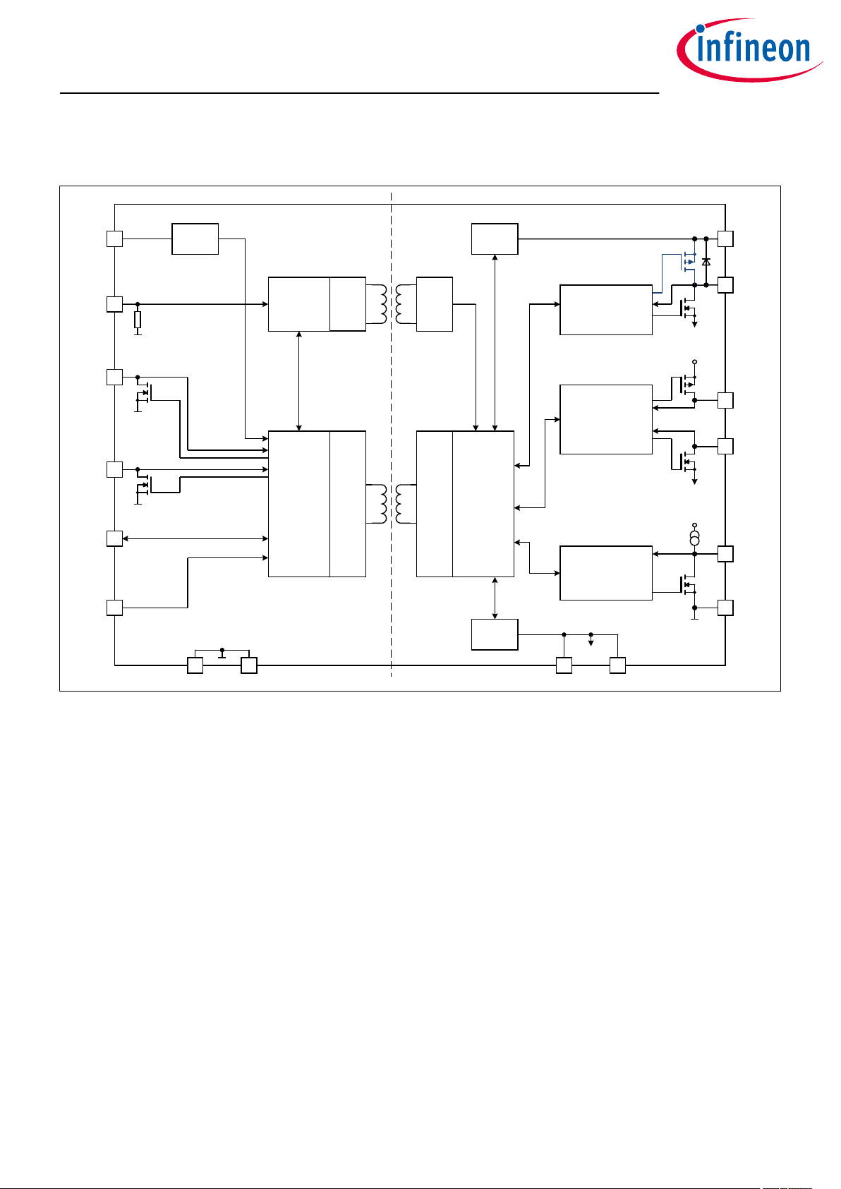
1 Block diagram
1 Block diagram
VCC1
FLT_N
RDYC
SDA
SCL
2
IN
7
UVLO1
PWM logic
1
TX
RX
UVLO2
CLAMP control,
monitoring, and
ADC input
opt.
VEE2
VCC2
14
10
VCC2
CLAMP
6
Output control
1
and monitoring
with hard-
12
ON
switching, TLTOff,
and SoftOff
11
OFF
5
VEE2
1
TRXLOGIC
TRX LOGIC
VCC2
4
DESAT
13
DESAT control
and monitoring
3
2
15
GND2
UVLO3
1
GND1
1
8 9 16
GND1
VEE2
VEE2 VEE2
Figure 2 Block diagram
Reference manual 6 v2.1
2021-02-15
Page 7

EiceDRIVER™ 1ED38x0Mc12M Enhanced
Reference manual
2 Related products
2 Related products
Note: Please consider the gate driver IC power dissipation and insulation requirements for the selected
power switch and operating condition.
Product group Product name Description
TRENCHSTOP
IGBT Discrete
™
IKQ75N120CS6 High Speed 1200 V, 75 A IGBT with anti-parallel diode in TO247-3
IKW15N120BH6 High Speed 1200 V, 15 A IGBT with anti-parallel diode in TO247
IHW40N120R5 Reverse conducting 1200 V, 40 A IH IGBT with integrated diode in
TO247
CoolSiC™ SiC
MOSFET Discrete
CoolSiC™ SiC
MOSFET Module
TRENCHSTOP
™
IGBT Modules
IMBF170R650M1 1700 V, 650 mΩ SiC MOSFET in TO263-7 package
IMW120R045M1 1200 V, 45 mΩ SiC MOSFET in TO247-3 package
IMZ120R350M1H 1200 V, 350 mΩ SiC MOSFET in TO247-4 package
IMZA65R027M1H 650 V, 27 mΩ SiC MOSFET in TO247-4 package
IMW65R107M1H 650 V, 107 mΩ SiC MOSFET in TO247-3 package
FS45MR12W1M1_B11 EasyPACK™ 1B 1200 V / 45 mΩ sixpack module
FF6MR12W2M1_B11 EasyDUAL™ 2B 1200 V, 6 mΩ half-bridge module
F3L11MR12W2M1_B74 EasyPACK™ 2B 1200 V, 11 mΩ 3-Level module in Advanced NPC
(ANPC) topology
F4-23MR12W1M1_B11 EasyPACK™ 1B 1200 V, 23 mΩ fourpack module
F4-200R17N3E4 EconoPACK™ 3 1700 V, 200 A fourpack IGBT module
FS150R17N3E4 EconoPACK™ 3 1700 V, 150 A sixpack IGBT module
FF650R17IE4 PrimePACK™ 3 1700 V, 650 A half-bridge dual IGBT module
FF1000R17IE4 PrimePACK™ 3 1700 V, 1000 A half-bridge dual IGBT module
FF1200R17IP5 PrimePACK™ 3+ 1700 V, 1200 A dual IGBT module
FF1500R17IP5 PrimePACK™ 3+ 1700 V, 1500 A dual IGBT module
FF1500R17IP5R PrimePACK™ 3 1700 V, 1500 A dual IGBT module
FF1800R17IP5 PrimePACK™ 3+ 1700 V, 1800 A dual IGBT module
FP10R12W1T7_B11 EasyPIM™ 1B 1200 V, 10 A three phase input rectifier PIM IGBT
module
FS100R12W2T7_B11 EasyPACK™ 2B 1200 V, 100 A sixpack IGBT module
FP150R12KT4_B11 EconoPIM™ 3 1200V three-phase PIM IGBT module
FS200R12KT4R_B11 EconoPACK™ 3 1200 V, 200 A sixpack IGBT module
Reference manual 7 v2.1
2021-02-15
Page 8

™
EiceDRIVER
1ED38x0Mc12M Enhanced
Reference manual
3 Functional description
3 Functional description
The 1ED38x0Mc12M family (X3 Digital) consists of galvanically isolated single channel gate driver ICs with an
extensive digital adjustable feature parameter set. All adjustments are done from low voltage input side during
start up via I2C bus. The configuration is stored into registers.
To start-up the gate driver IC for normal operation both input and output sides of the gate driver IC need to be
powered.
The 1ED38x0Mc12M family (X3 Digital) is designed to support various supply configurations on the input and
output side. On the output side unipolar and bipolar supply is possible.
The output stage is realized as rail-to-rail. There the gate driver voltage follows the supply voltage without an
additional voltage drop. In addition it provides an easy clamping of the gate voltage during short circuit of an
external IGBT.
The RDYC status output reports correct operation of the gate driver IC like suicient voltage supply. The FLT_N
status output reports failures in the application like desaturation detection.
To ensure safe operation the gate driver IC is equipped with an input and output side under-voltage lockout
circuit. The UVLO levels are optimized for IGBTs and MOSFETs, and are adjustable.
The desaturation detection circuit protects the external IGBT from destruction at a short circuit. The gate driver
IC reacts on a DESAT fault by turning o the IGBT with one of the following configurable turn-o methods:
• two-level turn-o
• adjustable so-o
• hard switch-o
The two-level turn-o (TLTO) is a voltage controlled turn-o function.
The so turn-o function is used to switch-o the external IGBT in overcurrent conditions in a so-controlled
manner to protect the IGBT against collector emitter over-voltages.
An adjustable active Miller clamp function protects the IGBT from parasitic turn-on in fast switching
applications.
The 1ED38x0 family also oers several measurement and monitoring functions. The monitoring functions can
be divided into:
• hardware based functions and
• ADC measurement based functions.
3.1 Start-up and fault clearing
For normal operation both input and output sides of the gate driver IC need to be powered. A low level at the
FLT_N pin always indicates a fault condition. In this case the IC starts internal mechanisms for fault clearing.
Input side start-up
1. Voltage at VCC1 reaches the input UVLO threshold: input side of gate driver IC starts operating
2. FLT_N follows input supply voltage
3. Input side is ready to communicate across I2C bus, awaiting user gate driver parameter configuration
4. Records parameters received across the I2C bus
5. Waits until output side is powered
6. Initiates internal start-up: Transfers configured values to output side
7. Performs internal self-test
The complete start-up time t
Output side start-up
1. Voltage at VCC2 reaches the output UVLO threshold: output side of gate driver IC starts operating
2. Activates OFF gate driver output: connected gate stays discharged
3. Waits until input side is powered
Reference manual 8 v2.1
depends on the duration of the user parameter configuration.
START1
2021-02-15
Page 9
EiceDRIVER
™
1ED38x0Mc12M Enhanced
Reference manual
3 Functional description
4. Initiates internal start-up: Receives configured values from input side
5. Performs internal self-test
The complete start-up time t
The gate driver IC releases RDYC to high to signal a successful start-up and its readiness to operate. The gate
driver IC will follow the status of the IN signal.
Clearing a fault with RDYC to low cycle
1. Set IN to low
2. Set RDYC to low for a duration longer than the fault clear time t
3. Release RDYC to high
a. If the source of the fault is no longer present, FLT_N is released to high
b. If another fault source is active, FLT_N stays low and the cycle needs to be repeated
4. Continue PWM operation
Clearing a fault by self clear timer
depends on the duration of the user parameter configuration.
START2
CLRMIN
1. Set IN to low
2. Self clear timer starts counting
3. Self clear timer reaches self clear time
a. If the source of the fault is no longer present, FLT_N is released to high
b. If another fault source is active, FLT_N stays low and the timer restarts
4. Continue PWM operation
3.2 Supply
The 1ED38x0Mc12M family (X3 Digital) is designed to support various supply configurations. The input side can
be used with a 3.3 V or 5 V supply.
The output side requires either an unipolar supply (VEE2 = GND2) or a bipolar supply.
• Individual supply voltages between VCC2 and GND2 or GND2 and VEE2 shall not exceed 25 V.
• The total supply voltage between VCC2 and VEE2 shall not exceed 35 V.
To ensure safe operation of the gate driver IC, it is equipped with an input and output side undervoltage lockout
circuit.
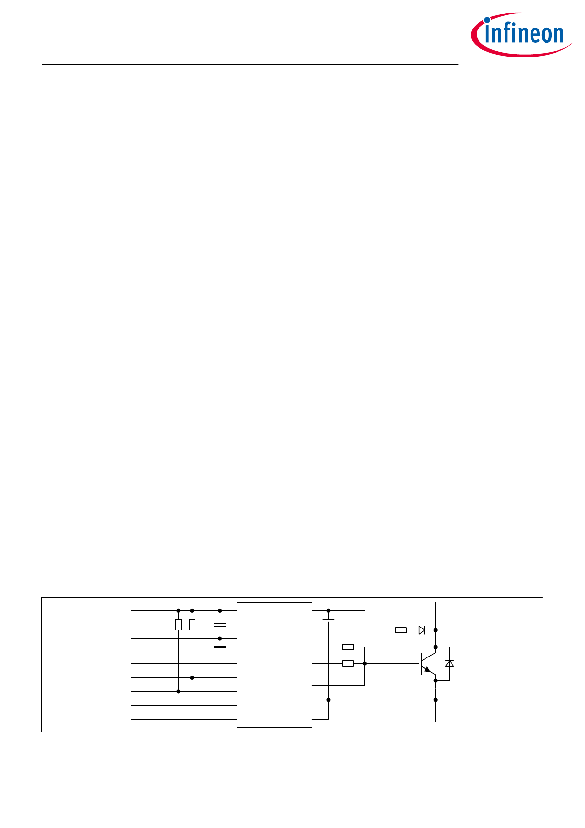
Unipolar supply
In unipolar supply configuration the gate driver IC is typically supplied with a positive voltage of 15 V at VCC2.
GND2 and VEE2 are connected together and this common potential is connected to the IGBT emitter.
+3V3
SGND
IN
RDYC
FLT_N
SCL
SDA
10k
10k
VCC1
GND1
IN
RDYC
FLT_N
SCL
SDA
VCC2
DESAT
ON
OFF
CLAMP
GND2
VEE2
+15V
1µ100n
1k
1R
1R
Figure 3 Application example with unipolar supply
Reference manual 9 v2.1
2021-02-15
Page 10
EiceDRIVER
™
1ED38x0Mc12M Enhanced
Reference manual
3 Functional description
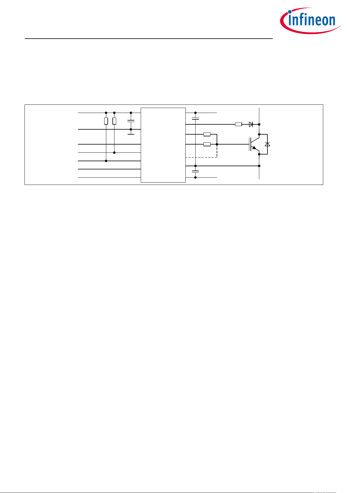
Bipolar supply
For bipolar supply the gate driver IC is typically supplied with a positive voltage of 15 V at VCC2 and a negative
voltage of -8 V or -15 V at VEE2 relative to GND2.
Between VCC2 and VEE2 the maximum potential dierence is 35 V.
+3V3
SGND
IN
RDYC
FLT_N
SCL
SDA
10k
10k
100n
VCC1
GND1
IN
RDYC
FLT_N
SCL
SDA
VCC2
DESAT
ON
OFF
CLAMP
GND2
VEE2
+15V
1µ
1µ
1k
1R
1R
-8V
Figure 4 Application example with bipolar supply
Negative supply prevents a parasitic turn-on due to the additional voltage margin to the gate turn-on threshold.
VEE2 over GND2 supply connection check
The gate driver IC has a built-in connection check for VEE2. A loss of VEE2 connection will be detected and
signaled via RDYC.
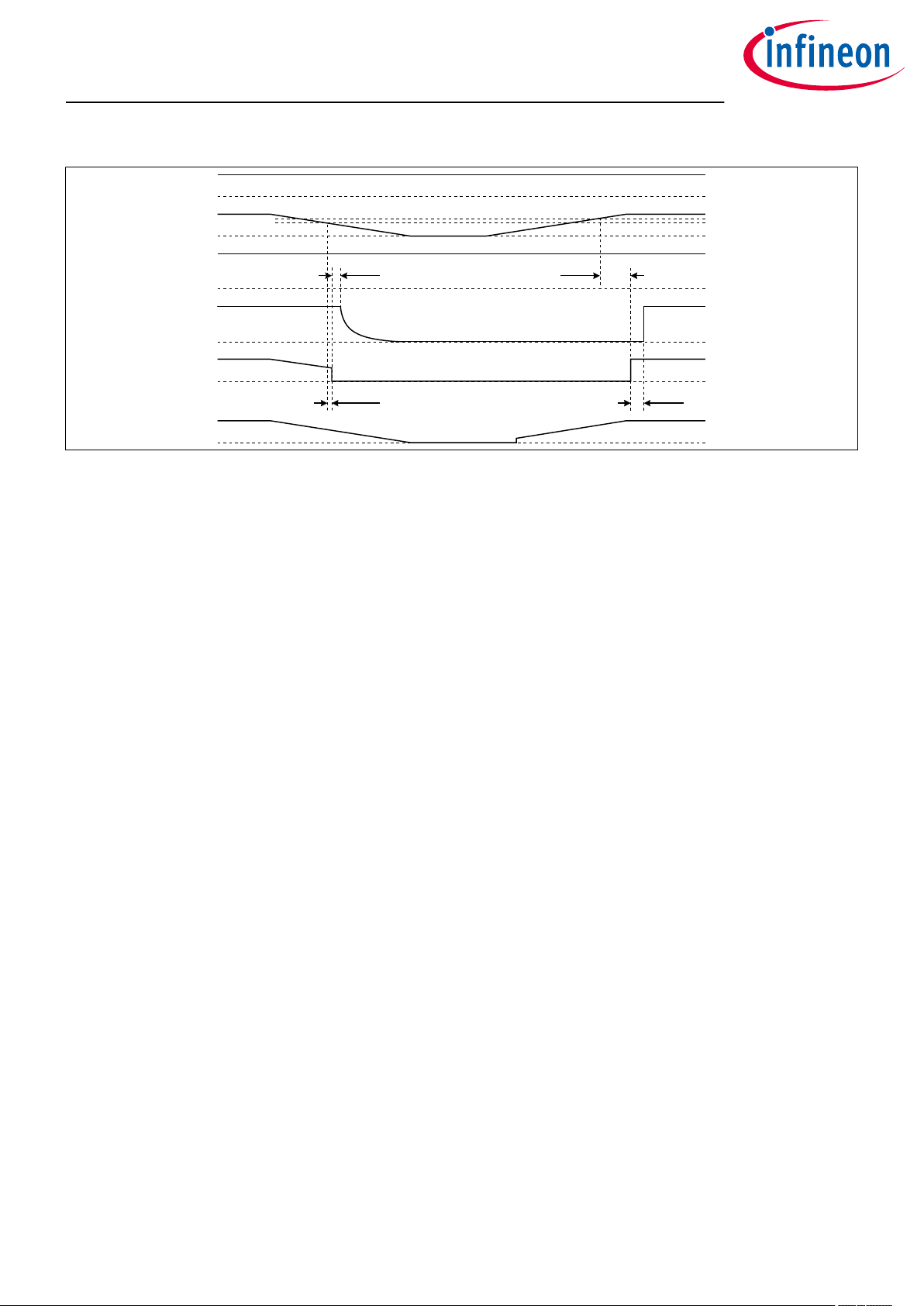
3.2.1 Input side undervoltage lockout, VCC1 UVLO
To ensure correct operation of the input side and safe operation of the application the gate driver IC is equipped
with an input supply undervoltage lockout for VCC1.
UVLO behavior during start-up:
1. The voltage at the supply terminal VCC1 reaches the V
2. The gate driver IC waits on the address and parameter configuration and synchronizes it with the output
side
3. The IC releases the RDYC output to high and is ready to operate.
The complete start-up time t
depends on the duration of the user parameter configuration.
START1
UVLO behavior during shut-down:
• If the supply voltage V
of the input side drops below V
VCC1
output will be switched o.
The fault signal FLT_N follows the input supply voltage.
UVLO1H
UVLO1L
threshold
the RDYC signal is switched to low and the
Reference manual 10 v2.1
2021-02-15
Page 11
EiceDRIVER
™
1ED38x0Mc12M Enhanced
Reference manual
3 Functional description
IN
VCC1
V
V
UVLO1H
UVLO1L
VCC2
ON+OFF
RDYC
FLT_N
t
t
UV1LRDYC
PDRDYC
t
START1
t
PDRDYC
Figure 5 UVLO VCC1 behavior
The gate driver IC supports an alternative UVLO detection in order to provide the means of analyzing the quality
of the VCC1 power supply. The number of unfiltered UVLO comparator output transitions is stored in the register
UV1FCNT.UV1F_CNT and can be read out via I2C bus.
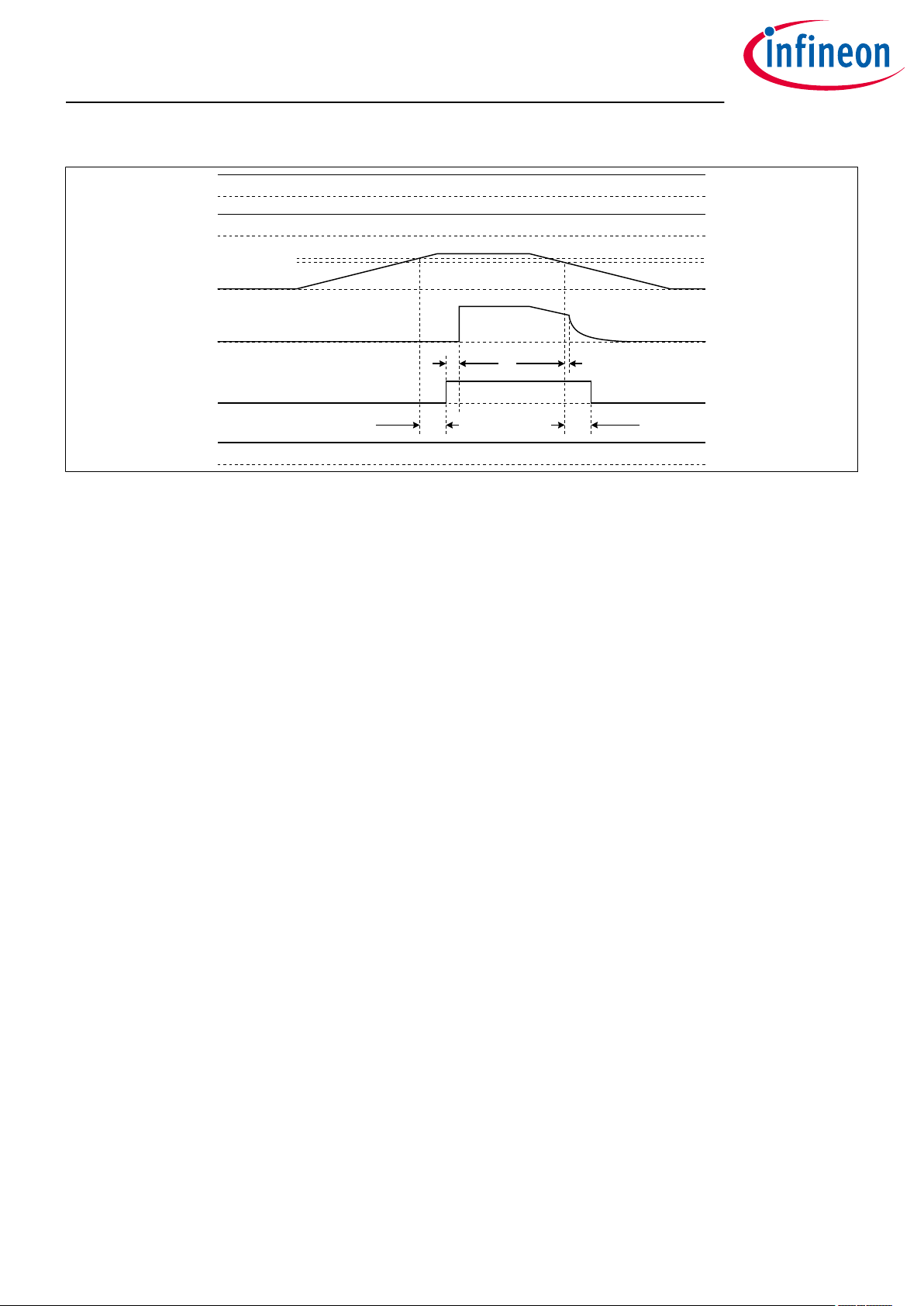
3.2.2 Output side under-voltage lockout, VCC2 UVLO
To ensure correct operation of the output side and safe operation of the IGBT in the application, the gate driver
IC is equipped with an output supply undervoltage lockout for VCC2 versus GND2.
UVLO behavior during start-up:
• If the voltage at the supply terminal VCC2 reaches the V
transfer the input side configuration to the output side before the RDYC output is released to high.
• The rising voltage at the output side triggers a so-reset at the input side unless
- a new set of parameters has been written while the output side was o or
- the RECOVER.RESTORE bit was already set to 1B.
In that cases, the gate driver transfers the configuration to the output side and releases the RDYC output to
high.
The complete start-up time t
depends on the duration of the user parameter configuration.
START2
UVLO behavior during shut-down:
• If the supply voltage V
of the output side drops below V
VCC2
output will be switched o.
threshold the gate driver first needs to
UVLO2H
the RDYC signal is switched to low and the
UVLO2L
Reference manual 11 v2.1
2021-02-15
Page 12
EiceDRIVER
™
1ED38x0Mc12M Enhanced
Reference manual
3 Functional description
IN
VCC1
V
UVLO2H
V
UVLO2L
VCC2
ON+OFF
RDYC
FLT_N
Figure 6 UVLO VCC2 behavior
t
START2
t
PDRDYC
t
UV2LOFF
t
UV2LRDYC
Any V
event will lead to a fault-o and a RDYC low level. The actual UVLO threshold selection is done in
UVLO2L
register UVTLVL.UVVCC2TL. Going below this threshold will set the UVLO event register bit SECUVEVT.UV_VCC2.
If the supply voltage drops further the output side resets and needs a restart to configure its parameters again.
If the supply voltage recovers immediately without triggering a reset the gate driver IC will also release RDYC to
high.
The gate driver IC is supporting an alternative UVLO detection in order to provide the means of analyzing the
quality of the VCC2 power supply. The number of unfiltered UVLO2 comparator output transitions is stored in
the register UV2FCNT.UV2F_CNT and can be read out via I2C bus.
In addition the 1ED38x0 family oers the feature to measure, monitor and readout the VCC2 voltage through an
integrated ADC to tune the system behavior and adjust according to system/IGBT requirements.
3.2.3 Output side undervoltage lockout, VEE2 UVLO
The 1ED38x0 family oers three adjustable UVLO thresholds for the negative VEE2 supply rail tailored for the
typical operation conditions like -5 V or -8 V or -15 V supply versus GND2. Start up/shut down behavior is
identical to a VCC2 UVLO event assuming the VEE2 UVLO is configured.
VEE2 UVLO is handled in the undervoltage event register SECUVEVT.UV_VEE2, an V
fault o and a RDYC low level. Configure the negative UVLO level in register UVTLVL.UVVEE2TL. A 00B in this
register disables the VEE2 UVLO, e.g. for unipolar supply.
In addition the 1ED38x0 family oers the feature to measure, monitor, and readout the VEE2 voltage through an
integrated ADC to tune the system behavior and adjust according to system/IGBT requirements.
event will lead to a
UVLO3L
Reference manual 12 v2.1
2021-02-15
Page 13

EiceDRIVER™ 1ED38x0Mc12M Enhanced
Reference manual
3 Functional description
3.3 Input side logic
The input threshold levels are always CMOS compliant. The threshold levels are 30% of VCC1 for low level and
70% of VCC1 for high level.
The pins IN and SCL are for input only, and the pins SDA, FLT_N, and RDYC are input/output pins.
3.3.1 IN non-inverting driver input
The input pin has a positive logic. To turn on the associated IGBT apply a logic high signal at the IN pin. The
1ED38x0 family oers the adjustment of the IN input filter time with two trimmed values of typical 103 ns and
183 ns, as described in register PSUPR. The selected filter time directly influences the propagation delay.
3.3.2 RDYC ready status output, fault-o and fault clear input
The RDYC pin is a logic input and open drain output and has three dierent functions:
• RDYC as ready status output of all ready sources
• RDYC as fault-o input
• RDYC as fault clear input
In a typical application the RDYC pins of all gate driver ICs in the inverter are connected together and form a
single wire RDYC signal.
An external pull-up resistor is required to ensure RDYC status output during operation.
3.3.2.1 Ready sources and configuration of not ready events
Not ready events are signaled at RDYC pin by switching the pin voltage to GND1. The gate driver oers
configurable and non configurable not ready events.
Table 1 Ready sources and configuration registers
Ready source Status register bit(s) Configuration register
bit(s)
Internal signal
transmission
VEE2 over GND2 n.a. - gate driver in reset n.a. non-configurable, always
VCC1 supply UVLO n.a. - gate driver in reset n.a. non-configurable, always
VCC2 supply UVLO
VCC2 supply so UVLO
1)
COMERRST .CRC_PRI, .CR
C_SEC, .PCT_COM, .CRC_C
OM, .DCT_COM
SECUVEVT.UV_VCC2 n.a. non-configurable, always
2)
SECUVEVT.UVSVCC2 UVSVCC2C.UVSVCC2E 1B enables so UVLO
n.a. non-configurable, always
UVSVCC2C.UVSVCC2L configures so UVLO level
Configuration
description
enabled
enabled
enabled
enabled
monitoring
ADCCFG.VINT_EN 1B enables ADC for
internal voltages
VEE2 supply UVLO
Reference manual 13 v2.1
1)
SECUVEVT.UV_VEE2 UVTLVL.UVVEE2TL >0D enables UVLO
monitoring
2021-02-15
Page 14
™
EiceDRIVER
1ED38x0Mc12M Enhanced
Reference manual
3 Functional description
Table 1 Ready sources and configuration registers (continued)
Ready source Status register bit(s) Configuration register
bit(s)
VEE2 supply so UVLO
2)
SECUVEVT.UVSVEE2 UVSVEE2C.UVSVEE2E 1B enables so UVLO
Configuration
description
monitoring
UVSVEE2C.UVSVEE2L configures so UVLO level
ADCCFG.VINT_EN 1B enables ADC for
internal voltages
Gate driver configuration CHIPSTAT.CONFIG,
CHIPSTAT.ACTIVE
I2CCFGOK.I2CCFGOK 1B locks user address
configuration
CFGOK.USER_OK 1B locks user
configuration
1) A complete loss of secondary supply voltage followed by a power-up can result in a so-reset on the input
side requiring a parameter re-configuration.
2) If so UVLO is enabled, but ADC measurement is not enabled a so UVLO event will be signaled due to ADC
output value of 00H.
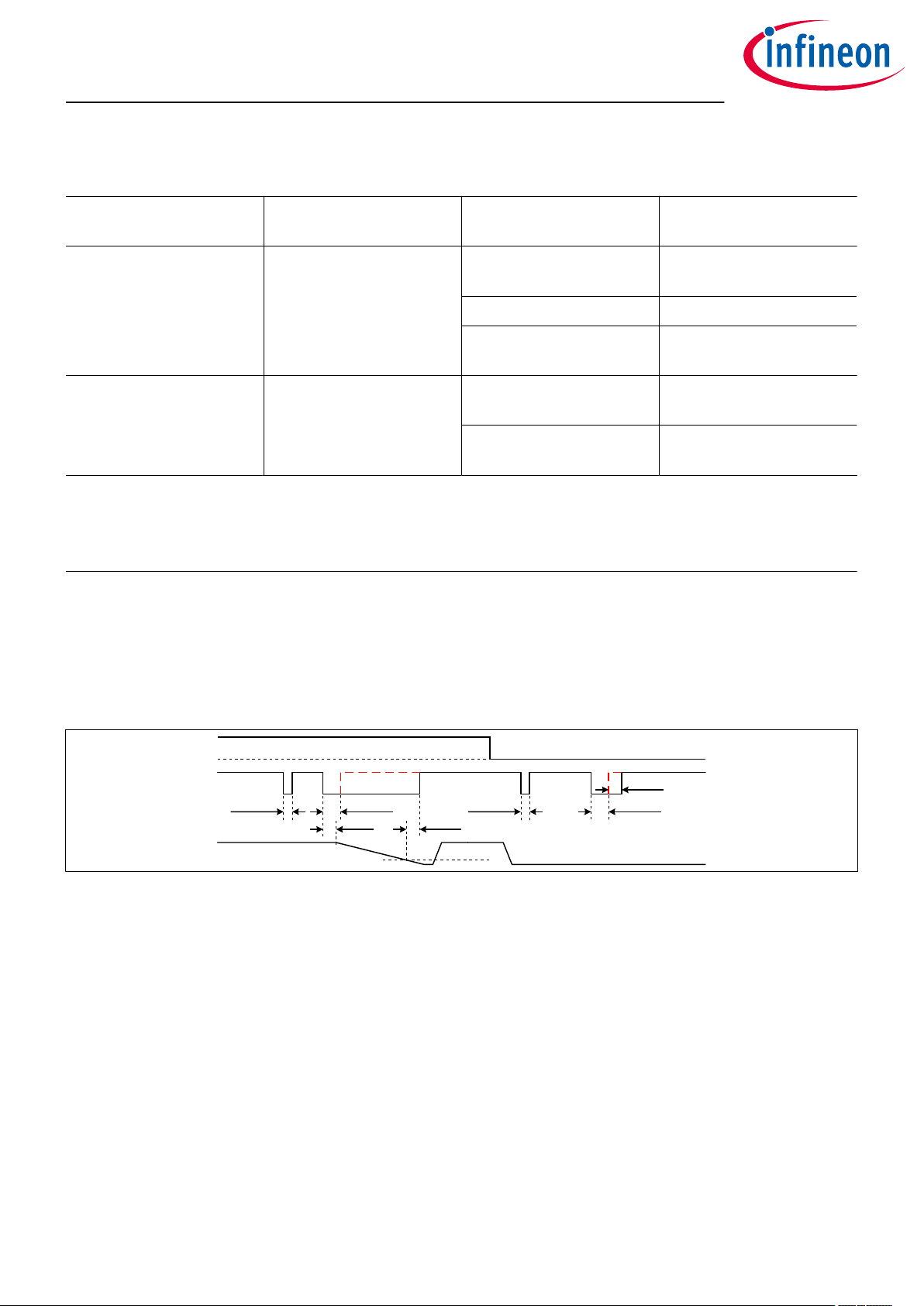
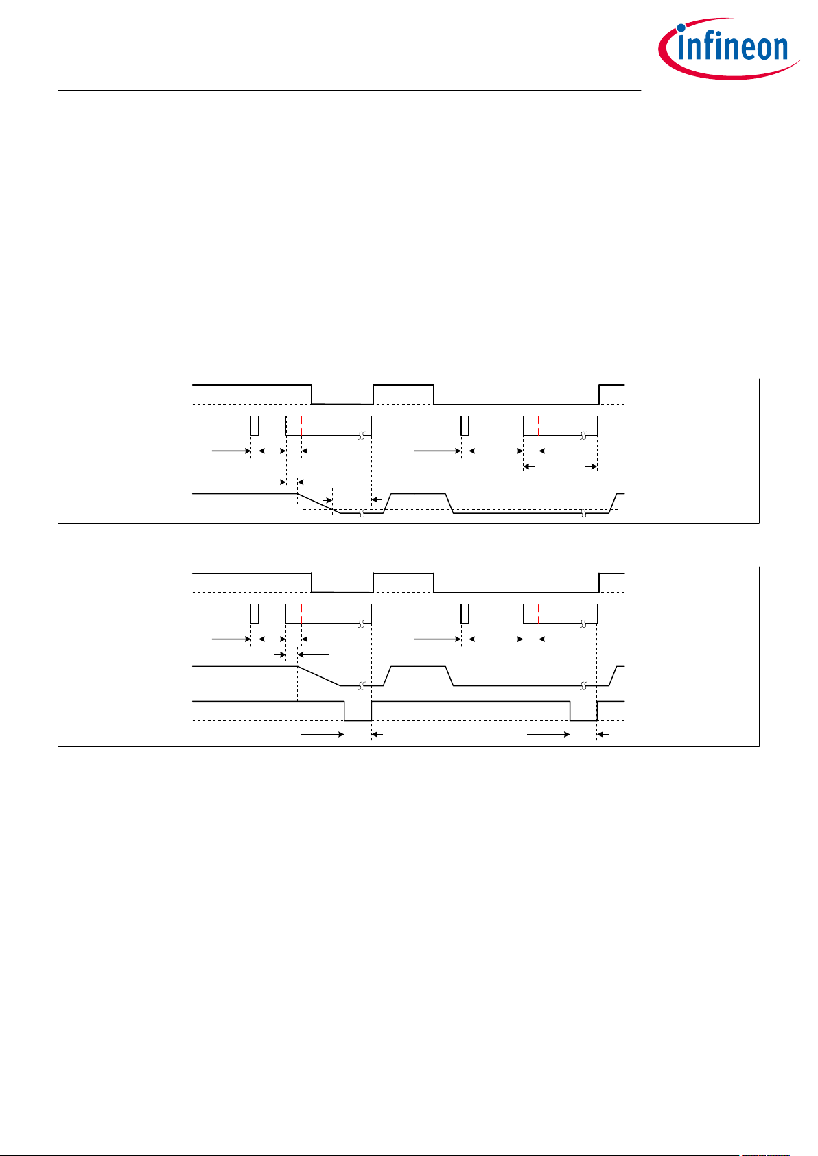
3.3.2.2 RDYC fault-o input
Pulling RDYC to low disables the operation of the gate driver IC. The gate driver IC ignores IN signals as long as
the RDYC pin stays low and the IC uses its fault-o function to switch-o the IGBT.
The defined minimum adjustable pulse width (PSUPR.IN_SUPR) makes the IC robust against glitches at RDYC.
The gate driver ignores pulses with a shorter duration.
IN
RDYC
<t
RDYCMIN
ON+OFF
RDYC ext.
>t
RDYCMIN
t
PDRDYC
t
SSIO
VEE2 + 2V
<t
RDYCMIN
>t
t
SSIO
RDYCMIN
Figure 7 RDYC short pulse behavior of external manipulation of the RDYC pin
Aer
an external RDYC low signal the IC is actively pulling RDYC to low until the voltage at ON pin falls below the
VEE2+2 V threshold.
The RDYC fault-o input is active low.
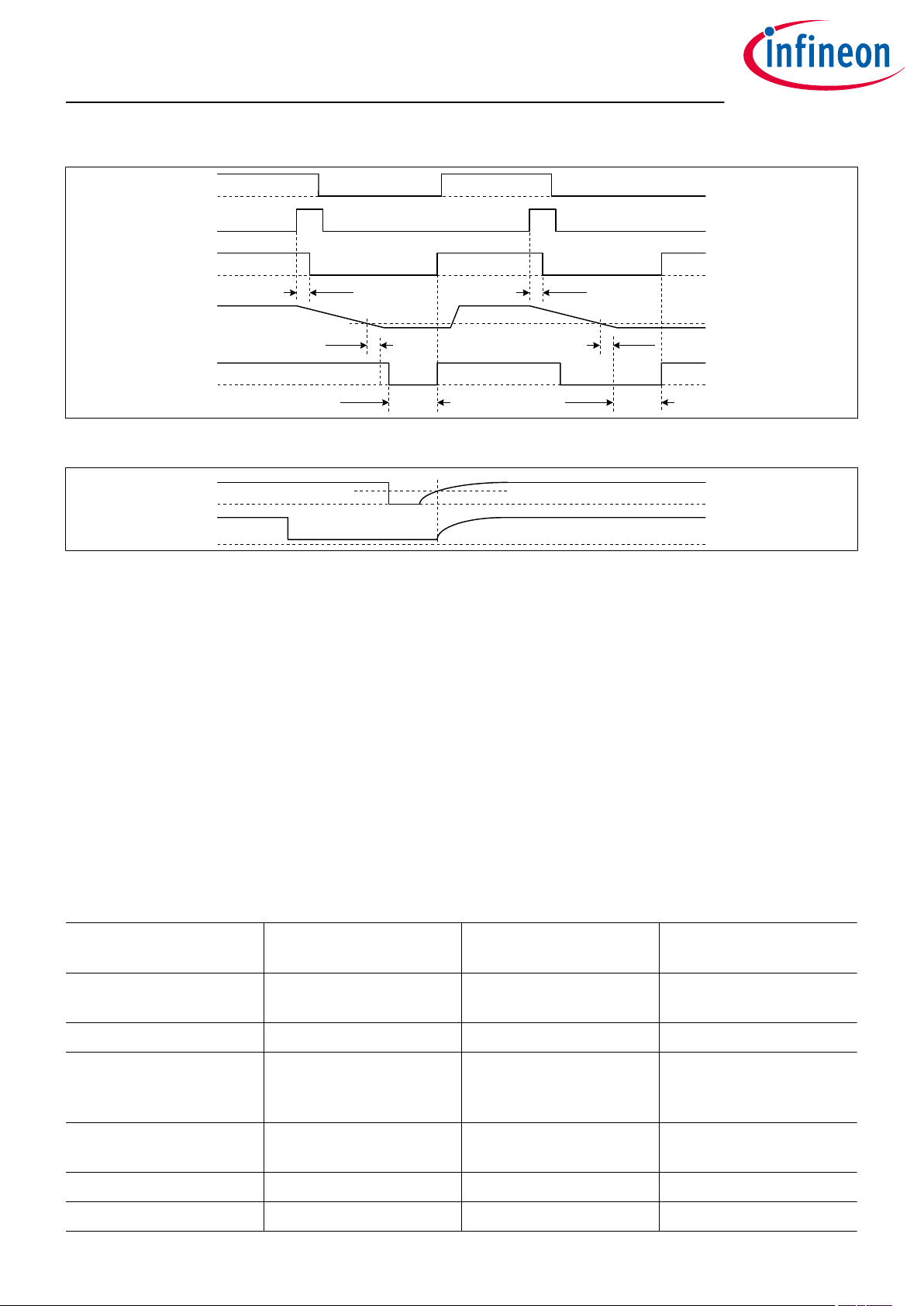
3.3.2.3 RDYC fault clear input
To use the RDYC as fault clear input, the register bit FCLR.FCLR_CFG needs to be 0B. Setting RDYC to low for
longer than the fault clear time t
Additionally the following conditions have to be met as well:
• PWM IN pin level needs to be low,
• voltage at ON pin has dropped below the VEE2+2 V threshold, and
• triggering fault condition is no longer present.
The typical fault clear time t
CLRMIN
will reset the stored fault signal at pin FLT_N with the rising edge of RDYC.
CLRMIN
is 1.0 µs.
Reference manual 14 v2.1
2021-02-15
Page 15
EiceDRIVER™ 1ED38x0Mc12M Enhanced
Reference manual
3 Functional description
IN
FLT event
FLT_N
t
DESATFLT
t
DESATFLT
SSIO
>t
CLRMIN
VEE2 + 2V
>t
CLRMIN
t
SSIO
ON+OFF
t
RDYC
Figure 8 RDYC fault clear timing
V
RDYC
FLT_N
IH
Figure 9 RDYC fault clear rising edge to FLT_N
3.3.3 FLT_N status output and fault-o input
The FLT_N pin is a logic input and open drain output and has two dierent functions:
• FLT_N as fault-status output for fault sources
• FLT_N as fault-o input
In a typical application the FLT_N pins of all gate driver ICs in the inverter are connected together and form a
single wire FLT_N signal.
An external pull-up-resistor is required to ensure FLT_N status output during operation.
3.3.3.1 Fault sources and configuration of fault events
Fault events are signaled at FLT_N pin by switching the pin voltage level to GND1. The gate driver oers
configurable and non-configurable fault events.
Table 2 Fault sources and configuration registers
Fault source Status register bit(s) Configuration register
bit
Over temperature
FLTEVT .OTP_EVT n.a. non-configurable, always
protection
Over temperature warning FLTEVT.OTW_EVT OTWCFG.OTW_ACFG 0B disables OTW event
Desaturation detection of
FLTEVT .D1_EVT, .D2_EVT D1LVL.D_DIS 1B disables DESAT
IGBT
Secondary desaturation
FLTEVT.D2_EVT D2LVL.D2_ACFG 0B disables DESAT2 event
detection of IGBT
Switch-o timeout FLTEVT.SOTO_EVT SOTOUT.SOTOUT_F 0B disables timeout event
CLAMP pin voltage limit FLTEVT.VEXTFLT ADCCFG.VEXTL_EN 0B disables limit event
Reference manual 15 v2.1
Configuration
description
enabled
completely, no event
monitoring
2021-02-15
Page 16
™
EiceDRIVER
1ED38x0Mc12M Enhanced
Reference manual
3 Functional description
The status register bits still highlight a possible fault event even if their configuration register disables the
triggering of FLT_N. The desaturation detection configuration with register bit D1LVL.D_DIS however disables
this part of the integrated circuit and therefore disables also both DESAT events.
3.3.3.2 FLT_N fault-o input
Pulling FLT_N to low disables the operation of the gate driver IC. The gate driver IC ignores IN signals as long as
the FLT_N pin stays low and the IC uses its fault-o function to switch-o the IGBT.
The defined minimum adjustable pulse width (PSUPR.IN_SUPR) makes the gate driver IC robust against glitches
at FLT_N.
Aer a low at the FLT_N pin either internally or externally applied, the fault event is latched until cleared.
The FLT_N fault-o input is active low.
IN
FLT_N
<t
FLT_NMIN
ON+OFF
FLT_N ext. FLT_N ext.
>t
FLT_NMIN
t
PDFLT_N
t
SSIO
+t
FSCLR
<t
FLT_NMIN
VEE2 + 2V
t
SSIO
>t
FLT_NMIN
+t
FSCLR
Figure 10 FLT_N short pulse behavior of external manipulation of the FLT_N pin with self clear
IN
FLT_N
<t
FLT_NMIN
FLT_N ext. FLT_N ext.
>t
FLT_NMIN
t
PDFLT_N
<t
FLT_NMIN
>t
FLT_NMIN
ON+OFF
RDYC
>t
CLRMIN
>t
CLRMIN
Figure 11 FLT_N short pulse behavior of external manipulation of the FLT_N pin cleared by RDYC
3.3.4 I2C bus
The 1ED38x0 family is equipped with a standard I2C bus interface to configure various parameters of the gate
driver IC and read out measurement and monitoring registers.
Key I2C features include:
• I2C bus slave device implementing all mandatory slave bus protocols for the specification UM10204 rev. 6
• 7 bit device addresses for individual and group addressing
• Initial I2C device address: 1AH (MSB aligned, bits 7:1)
• Signal voltage level compatible to 3.3 V and 5 V
• Supported bus speeds at gate driver data pin (SDA) and clock pin (SCL):
- standard-mode (Sm), with bit rates up to 100 kbit/s
- fast-mode (Fm), with bit rates up to 400 kbit/s
- fast-mode plus (FM+), with bit rates up to 1 Mbit/s
Reference manual 16 v2.1
2021-02-15
Page 17
™
EiceDRIVER
1ED38x0Mc12M Enhanced
Reference manual
3 Functional description
SDA
SCL
SCL
filter
data valid data change data valid
time
SCL
filter
time
data change
SDA
SCL
S - start P - stop
Figure 12 Start, stop and data conditions
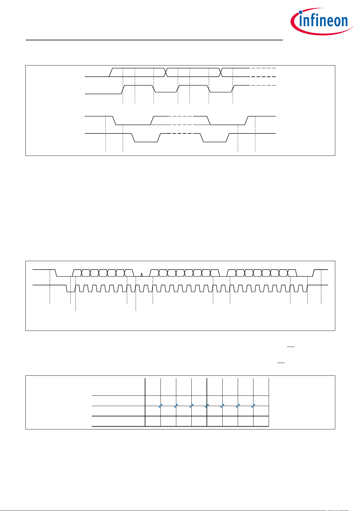
All I2C bus commands start with a start condition and stops with a stop condition. The data at the SDA pin gets
valid if SCL level is above the CMOS level threshold and the filter time has elapsed.
3.3.4.1 I2C bus byte format
All register addresses and data bytes of the 1ED38x0 family are 8 bit values. The serial data line (SDA) transmits
and receives with the most significant bit (MSB) first.
There are two register areas implemented:
• register addresses from 00H to 25H are used for configuration and
• register addresses from 26H to 37H are used as status registers.
MSB MSB MSBLSB LSB LSB
Wr
SDA
A6 A5 A4 A3 A2 A1 A0 R7 R6 R5 R4 R3 R2 R1 R0 Ack D7 D6 D5 D4 D3 D2 D1 D0 Ack
Ack
SCL
Start
Ack = Acknowledge
Wr = Write
Ax = Adress Bit
Rx = Register Bit
Dx = Data Bit
Slave address (7 bit)
Addressing byte (8 bit)
Register address (8 bit)
Data (8 bit) Stop
Figure 13 Write byte format (starting at register address)
The addressing byte is transmitted MSB first and includes the 7 bit I2C address followed by the Wr/Rd bit at
LSB position. Throughout this documentation, the hexadecimal device addresses are always written in this 8 bit
format. In the configuration registers the 7 bit I2C addresses are aligned to LSB without the
Bit
Address register byte
SDA addressing byte
Default address: 1A
MSB
7 6 5 4 3 2 1
res A6 A5 A4 A3 A2 A1 A0
A6 A5 A4 A3 A2 A1 A0 W/R
0 0 0 1 1 0 1 0
H
LSB
Wr/Rd bit.
0
Figure 14 I2C address alignment in register and during transmission
All registers have a data size of 8 bit, but not all bits are implemented in all registers. Not implemented data bits
read as 0B unless specified otherwise.
Reference manual 17 v2.1
2021-02-15
Page 18
™
EiceDRIVER
1ED38x0Mc12M Enhanced
Reference manual
3 Functional description
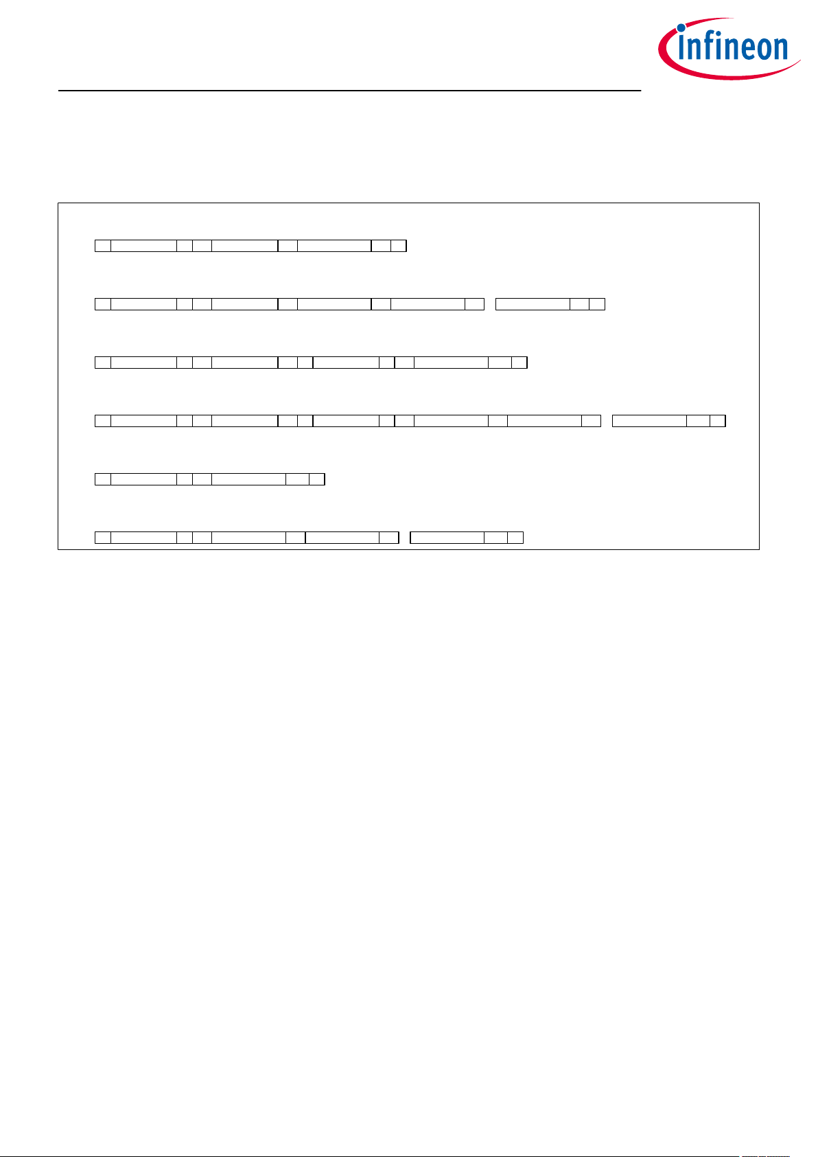
3.3.4.2 I2C bus read/write operation
Read and write operations are controlled by the I2C master (microcontroller).
Write byte (starting at specific register address)
1 7 1 1 8 1 8 1 1
S Slave address Wr Ack Register address Ack Data byte Ack P
Write n-bytes (starting at specific register address)
1 7 1 1 8 1 8 1
S Slave address Wr Ack Register address Ack Data byte (add.) Ack
Read byte (starting at specific register address)
1 7 1 1 8 1 7 1 11 8 1 1
S Slave address Wr Ack Register address Ack Data byte Nack PS Slave address AckRd
Read n-bytes (starting at specific register address)
1 7 1 1 8 1 7 1 11 8 1
S Slave address Wr Ack Register address Ack Data byte (add.) NackS Slave address AckRd
Data byte (add.+1)8Ack1Data byte (add.+n)8Ack
...
1
Ack
Data byte (add.+1)8Ack1Data byte (add.+n)
1
1
P
...
8
1
P
Read byte (starting at first status register)
1 7 1 1 8 1 1
S Slave address Rd Ack Data byte Nack P
Read n-bytes (starting at first status register)
1 7 1 1 8 1
S Slave address Rd Ack Data byte (add) Nack
1
Ack
Data byte (add+1)8Ack1Data byte (add+n)
...
8
1
P
Figure 15 Read/write operation
Write byte and write n-bytes to register
1. I2C master (microcontroller) to initiate write with start bit followed by 7 bit slave address (gate driver)
and write bit
2. Target gate driver answers with acknowledge (ACK)
3. Master to send 8 bit target register address
4. Target gate driver answers with ACK and sets internal register address
5. Master to send the data byte for current register
6. Target gate driver answers with ACK if target register is writable and increases internal register address by
1
H
7. Steps 5 and 6 can be repeated to send multiple bytes to consecutive registers
8. Master finalizes data write by sending a stop bit
Read byte and read n-bytes from specific register
1. I2C master (microcontroller) to initiate write with start bit followed by 7 bit slave address (gate driver)
and write bit
2. Target gate driver answers with acknowledge (ACK)
3. Master to send 8 bit target register address
4. Target gate driver answers with ACK and sets internal register address
5. Master begins new read session with start bit followed by 7 bit slave address (gate driver) and read bit
6. Target gate driver answers with acknowledge (ACK)
7. Target gate driver sends 8 bit data byte from current register and increases internal register address by 1
8. Master is responsible for ACK/NACK to control read of consecutive registers
a. When responding with ACK, the master is waiting for another data byte and the sequence
continues at number 7
b. When responding with NACK, the master terminates the read session
9. Master finalized data read by sending a stop bit
Reference manual 18 v2.1
2021-02-15
H
Page 19

™
EiceDRIVER
1ED38x0Mc12M Enhanced
Reference manual
3 Functional description
Read byte and read n-bytes from status register
1. I2C master (microcontroller) to initiate read with start bit followed by 7 bit slave address (gate driver) and
read bit
2. Without a preceding register write the gate driver sets the internal register address to the first status
register
3. Target gate driver answers with acknowledge (ACK)
4. Target gate driver sends 8 bit data byte from current register and increases internal register address by 1
5. Master is responsible for ACK/NACK to control read of consecutive registers
a. When responding with ACK, the master is waiting for another data byte and the sequence
continues at number 4
b. When responding with NACK, the master terminates the read session
6. Master finalized data read by sending a stop bit
3.3.4.3 I2C bus address
H
The gate driver IC has two configurable 7 bit addresses:
• device address I2CADD, e.g. for dedicated read out or configuration
• group address I2CGADD to configure all gate driver ICs in the same group within one write cycle
Both addresses have to be set at start up. Configured addresses have to dier from the initial LSB aligned I2C
device address 0DH.
Address configuration aer power up
The gate driver IC is configured to start up with the initial I2C device address. To set the device addresses the
input side has to be powered up and VCC1 is stable above the turn-on undervoltage lockout level. At this point,
the gate driver IC is still in OFF state.
Address configuration steps:
1. Set RDYC to low to deactivate the gate driver IC
2. Set IN to high to select the gate driver IC (chip select, IC enters address configuration state)
3. Send an I2C write command with 4 data bytes to the initial MSB aligned I2C device address 1A
H
a. Data byte 1: Target device register address 00H (RegisterI2CADD)
b. Data bytes 2, 3: 7 bit device address and 7 bit group address aligned from bit 6 to bit 0
c. Data byte 4: value for I2CCFGOK = 01H , to accept and lock the address registers
4. All data bytes will be acknowledged by the gate driver IC to indicate successful transmission and address
acceptance, the gate driver IC enters parameter configuration state
5. Release IN and RDYC, the gate driver IC is now addressable using the addresses transferred
Address configuration during gate driver operation
To re-configure the I2C addresses while the gate driver IC is already in normal operation mode it needs to be
switched to the address configuration state by executing the following steps:
1. Set RDYC to low, entering not ready state
2. Send an I2C write command with 2 data bytes to the current device address
a. Data byte 1: Target device register address 1CH (Register CFGOK)
b. Data byte 2: Value 00H, to enter parameter configuration state
3. Send again an I2C write command with 2 data bytes to the current device address
a. Data byte 1: Target device register address 02H (Register I2CCFGOK)
b. Data byte 2: Value 00H, to enter address configuration state and unlock address registers
4. Follow the steps 2 to 5 of the address configuration aer power up to complete the address re-
configuration
Reference manual 19 v2.1
2021-02-15
Page 20

EiceDRIVER™ 1ED38x0Mc12M Enhanced
Reference manual
3 Functional description
Address configuration notes
Attention: The gate driver IC does not acknowledge (NACK) a write of 01H to I2CCFGOK if the address
registers contain an invalid address.
Note: Reserved I2C bus addresses are not allowed but will be neither checked nor will the gate driver IC
send a NACK (not acknowledge) in response to such an address.
Reference manual 20 v2.1
2021-02-15
Page 21
™
EiceDRIVER
1ED38x0Mc12M Enhanced
Reference manual
3 Functional description
3.4 Operating states
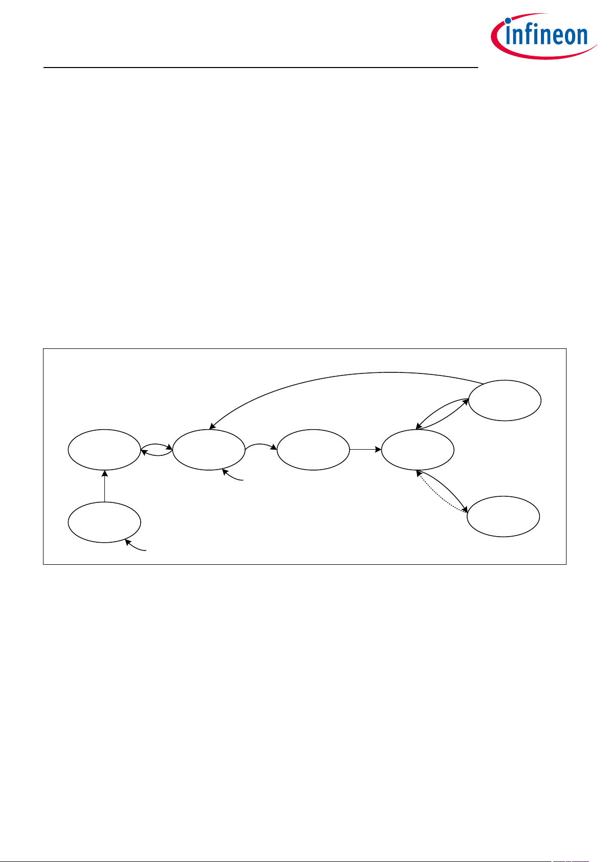
The 1ED38x0 family of gate driver ICs can take the following states:
• OFF state, device not powered
• Address configuration state, the I2C addresses can be set, gate driver IC is not active
• Parameter configuration state, the gate driver parameters can be set and changed, gate driver IC is not
active
• Parameter transfer state, the gate driver IC is transferring the parameters from input side to output side,
gate driver IC is not active
• Normal operation, gate driver IC is active, ON and OFF outputs are following the IN signal, registers are read
only
• Not ready state, gate driver IC is switched o according to fault o settings, status signaled by a low at RDYC
pin
• Fault state, gate driver IC is switched o according to fault o settings, status signaled by a low at FLT_N pin
• See later section for additional sub states on fault clear, so-reset, recover, and restore of parameter
configuration aer power loss
CFGOK.USER_OK = 0
Not Ready
State
VCC1 ok
RDYC = 0
FLT_N = x
IN = x
Fault State
RDYC = 1
FLT_N = 0
IN = x
Address
Configuration
State
Power on
OFF State
VCC1 nok
VCC2 nok
VCC1 ok
RDYC = 0
FLT_N = 1
IN = 1
I2CCFGOK.
I2CCFGOK
= 1
= 0
Parameter
Configuration
State
VCC1 ok
RDYC = 0
FLT_N = x
IN = x
CFGOK.
USER_OK
Soft-reset
= 1
Parameter
Transfer
State
VCC1 ok
VCC2 ok
RDYC = 0
FLT_N = x
IN = x
RDYSTAT.
SEC_RDY
= 1
Operation
VCC1 ok
VCC2 ok
RDYC = 1
FLT_N = 1
IN = x
Normal
RDYC = 1
RDYC = 0
FLT_N = 0 or
.SEC_FLTN = 0
GFLTEVT
Fault clearing
Figure 16 Operating state diagram
• Pin names in uppercase italic letters, supply pin status listed as either okay (ok) or not okay (nok) and for
logic pins with low (0), high (1), or either (x)
• Register names in uppercase bold letters followed by the register bit name and value
• States in bubbles with transitions marked by arrows with conditions attached
3.4.1 OFF state
The OFF state is the default state of a non-powered gate driver IC. No operation is possible.
• Input side is not powered.
• Output side is o while powered or in active shut down while unpowered.
• All commands besides input chip power-up are ignored.
Signal condition to enter state:
• VCC1 power down
Reference manual 21 v2.1
2021-02-15
Page 22

™
EiceDRIVER
1ED38x0Mc12M Enhanced
Reference manual
3 Functional description
Signal condition to leave state:
• to address configuration state: VCC1 power ok, VCC1 has passed upper UVLO1 threshold, IN is high
3.4.2 Address configuration state
The address configuration state is used to enter or change the I2C device address and is the first state aer the
OFF state. The gate driver IC is ready to receive the device addresses.
Register access in this state:
• I2CADD, I2C device address: read/write
• I2CGADD, group address: read/write
• I2CCFGOK, address configuration access lock register: read/write
Signal condition to enter state:
• from OFF state: VCC1 power ok, VCC1 is passing upper UVLO1 threshold, IN is high
• from parameter configuration state: register bit I2CCFGOK.I2CCFGOK set to 0
Signal condition to leave state:
• to parameter configuration state: registers I2CADD and I2CGADD set according to the I2C and gate driver IC
address requirements, register bit I2CCFGOK.I2CCFGOK set to 1
B
B
3.4.3 Parameter configuration state
The parameter configuration state is used to configure or change device function and parameter and is the
default state aer address configuration state.
Register access in this state:
• address registers: read only
• I2CCFGOK: read/write
• configuration registers: read/write
• status register: read only
Signal condition to enter state:
• from address configuration state: register bit I2CCFGOK.I2CCFGOK set to 1
• from not ready state: register bit CFGOK.USER_OK set to 0
B
B
• from a so-reset
Signal condition to leave state:
• to parameter transfer state: register bit CFGOK.USER_OK set to 1
• to address configuration state: register bit I2CCFGOK.I2CCFGOK set to 0
B
B
3.4.4 Parameter transfer state
The parameter transfer state is used to transfer the configuration registers from primary to secondary side.
Register access in this state:
• status, configuration and address registers: read only
Signal condition to enter state:
• from parameter configuration state: register bit CFGOK .USER_OK set to 1
Signal condition to leave state:
• to normal operation state: VCC2/VEE2 power okay and register bit RDYSTAT.SEC_RDY set to 1
B
B
Reference manual 22 v2.1
2021-02-15
Page 23

EiceDRIVER
™
1ED38x0Mc12M Enhanced
Reference manual
3 Functional description
3.4.5 Normal operation state
The normal operation state is used for status register read and PWM operation.
Register access in this state:
• status, configuration and address registers: read only
Signal condition to enter state:
• from parameter transfer state: register bit RDYSTAT.SEC_RDY set to 1
• from fault state: intermediate states of fault clear flow
• from not ready state: RDYC signal released
Signal condition to leave state:
• to fault state: FLT_N signal externally pulled to low or register bit GFLTEVT.SEC_FLTN = 0B indicating a fault
source from output side
• to not ready state: RDYC signal pulled to low
B
3.4.6 Not ready state
The not ready state is used to indicate an inactive gate driver IC with PWM operation disabled.
Register access in this state:
• CFGOK register: read/write
• status, configuration and address registers: read only
Signal condition to enter state:
• from normal operation state: RDYC signal pulled to low
Signal condition to leave state:
• to normal operation state: RDYC signal released
• to parameter configuration state: CFGOK.USER_OK set to 0
B
3.4.7 Fault state
The fault state is used during and aer a fault turn o until the fault condition is cleared.
Register access in this state:
• status, configuration and address registers: read only
Signal condition to enter state:
• from normal operation state: FLT_N signal externally pulled to low or register bit GFLTEVT.SEC_FLTN = 0
indicating a fault source detected by the output side of the gate driver IC
Signal condition and flow to leave state:
B
Reference manual 23 v2.1
2021-02-15
Page 24
™
EiceDRIVER
1ED38x0Mc12M Enhanced
Reference manual
3 Functional description
FLT_N = 0 or
.SEC_FLTN = 0
GFLTEVT
t ≤ FCLR.FSCLR_T
GFLTEVT.SEC_FLTN = 1 &
FLTEVT.VOUT_ST = 0 &
Fault State
RDYC = 1
FLT_N = 0
IN = x
FCLR.FCLR_CFG = 1
IN = 0
GFLTEVT
.SEC_FLTN = 0
Fault Clear
Pending
RDYC = x
FLT_N = 0
IN = x
Figure 17 Fault clear using self clear timer
• Pin names in uppercase italic letters, supply pin status listed as either okay (ok) or not okay (nok) and for
logic pins with low (0), high (1), or either (x)
• Register names in uppercase bold letters followed by the register bit name and value
• States in bubbles with transitions marked by arrows with conditions attached
t > FCLR.FSCLR_T
& FLT_N = 1
Normal
Operation
RDYC = 1
FLT_N = 1
Register bit FCLR.FCLR_CFG = 1B (Fault clear using self-clear timer)
1. register bit GFLTEVT.SEC_FLTN = 1B, indicating that the fault source is no longer triggering and the fault
o sequence is completed
2. register bit FLTEVT.VOUT_ST = 0B, indicating that the output switch-o is done
3. IN pin switched to low to enter the fault clear pending state
4. staying in fault clear pending for the duration of the configured self clear time FCLR.FSCLR_T without
having a new fault trigger GFLTEVT.SEC_FLTN = 0
B
5. aer fulfilling the above conditions the gate driver IC releases the FLT_N pin and returns to normal
operation state
FLT_N = 0 or
.SEC_FLTN = 0
GFLTEVT
GFLTEVT.SEC_FLTN = 1 &
FLTEVT.VOUT_ST = 0 &
Fault State
RDYC = x
FLT_N = 0
IN = x
FCLR.FCLR_CFG = 0
RDYC = 0 &
IN = 0
GFLTEVT
.SEC_FLTN = 0
&
t ≤ t
CLRMIN
RDYC = 0
Fault Clear
Pending
RDYC = 0
FLT_N = 0
IN = x
t > t
CLRMIN
RDYC = 1 &
FLT_N = 1
&
Normal
Operation
RDYC = 1
FLT_N = 1
Figure 18 Fault clear using RDYC pin
• Pin names in uppercase italic letters, supply pin status listed as either okay (ok) or not okay (nok) and for
logic pins with low (0), high (1), or either (x)
• Register names in uppercase bold letters followed by the register bit name and value
• States in bubbles with transitions marked by arrows with conditions attached
Register bit FCLR.FCLR_CFG = 0B (Fault clear using RDYC pin)
1. register bit GFLTEVT.SEC_FLTN = 1B, indicating that the fault source is no longer triggering and the fault
o sequence is completed
2. register bit FLTEVT.VOUT_ST = 0B, indicating that the output switch-o is done
3. IN pin switched to low
4. RDYC pin switched to low to enter the fault clear pending state
Reference manual 24 v2.1
2021-02-15
Page 25

EiceDRIVER
™
1ED38x0Mc12M Enhanced
Reference manual
3 Functional description
5. staying in fault clear pending for the duration of the fault clear time t
trigger GFLTEVT.SEC_FLTN = 0
6. RDYC pin released to high
7. aer fulfilling the above conditions the gate driver releases the FLT_N pin and returns to normal
operation state
B
without having a new fault
CLRMIN
3.4.8 So-reset, restore and recovery
The 1ED38x0 family oers three configuration related modes:
• so-reset of all configuration registers to return to their reset values
• automatic restore of all output registers aer an output not ready event
• automatic recovery of all input registers aer an input not ready event
Both restore and recovery are independent and can be enabled at the same time. The automatic restore or
recovery can only work if one driver side stays supplied.
3.4.8.1 So-reset
The so-reset configuration register bit CLEARREG.SOFT_RST allows to clear all configuration registers. Unless
the automatic restore of output registers is configured, a so-reset will also be triggered aer a severe output
side UVLO event.
Aer a reset the registers will have their reset values and the gate driver IC returns to the parameter
configuration state. The I2C address registers I2CADD, I2CGADD, and I2CCFGOK will not be aected, only the
configuration registers need a new set of parameters.
3.4.8.2 Automatic configuration restore from input side
The gate driver IC is equipped with an advanced configuration restore function. If the output side lost its
configuration (e.g. VCC2 UVLO triggered so-reset) the input side is trying to restore the data from the input side
to the output side as soon as the output side is ready again.
The function is configured in register bit RECOVER.RESTORE
• 0B = restore not active, the gate driver IC will
- perform a so-reset,
- clear parameter configuration bit CFGOK.USER_OK to 0B, and
- stay in parameter configuration state and wait for the user to re-configure the settings
• 1B = restore active, the gate driver IC will
- restore the output side and
- release RDYC and enter normal operation state
Reference manual 25 v2.1
2021-02-15
Page 26

EiceDRIVER
™
1ED38x0Mc12M Enhanced
Reference manual
3 Functional description
Parameter
Configuration
State
VCC1 ok
RDYC = 0
FLT_N = x
IN = x
CFGOK.
USER_OK = 0
Output Side
Power Down
(not-ready)
State
VCC1 ok
VCC2 nok
RDYC = 0
I2CCFGOK.I2CCFGOK = 1
CFGOK.USER_OK = 1
RECOVER.RESTORE = 1
VCC2 -> ok
Parameter
Transfer
State
VCC1 ok
VCC2 ok
RDYC = 0
RDYSTAT.
SEC_RDY
= 1
Operation
VCC1 ok
VCC2 ok
RDYC = 1
FLT_N = 1
Normal
Figure 19 State diagram of output configuration restore from input side
• Pin names in uppercase italic letters, supply pin status listed as either okay (ok) or not okay (nok) and for
logic pins with low (0), high (1), or either (x)
• Register names in uppercase bold letters followed by the register bit name and value
• States in bubbles with transitions marked by arrows with conditions attached
The output side power down state is a not ready state where additional conditions apply. The regular path to
parameter configuration state is also possible. Otherwise the gate driver IC leaves this state to parameter
transfer state aer a successful output side power up. Aer the register transfer the status register bit
RDYSTAT.SEC_RDY will be set to 1B and the gate driver IC returns to normal operation state.
A successful restore will be signaled by the sticky bit in the register bit EVTSTICK.SRESTORE.
3.4.8.3 Automatic configuration recovery from output side
The gate driver IC is equipped with an advanced configuration recovery function. If the input side lost its
configuration (e.g. UVLO event at VCC1) the input side is trying to recover the data from the output side as soon
as the input side is ready again.
The function is configured in register RECOVER.RECOVER:
• 0B recover not active, gate driver IC will
- perform a so-reset,
- clear parameter configuration bit CFGOK.USER_OK and I2CCFGOK.I2CCFGOK to 0B, and
- returns to OFF state
• 1B recover active, gate driver IC will
- recover the configuration from the output side,
- release RDYC, and
- enter normal operation state
Input Side
Power Down
State
VCC1 nok
VCC2 ok
RDYC = 0
I2CCFGOK.I2CCFGOK = 1
CFGOK.USER_OK = 1
RECOVER.RECOVER = 1
VCC1 -> ok
Parameter
Transfer
State
VCC1 ok
VCC2 ok
RDYC = 0
RDYSTAT.
PRI_RDY
= 1
Operation
VCC1 ok
VCC2 ok
RDYC = 1
FLT_N = 1
Normal
Figure 20 State diagram of input configuration recover from output side
• Pin names in uppercase italic letters, supply pin status listed as either okay (ok) or not okay (nok) and for
logic pins with low (0), high (1), or either (x)
• Register names in uppercase bold letters followed by the register bit name and value
• States in bubbles with transitions marked by arrows with conditions attached
Reference manual 26 v2.1
2021-02-15
Page 27

™
EiceDRIVER
1ED38x0Mc12M Enhanced
Reference manual
3 Functional description
The input side power down state is an extended o state. The gate driver IC leaves this state to
parameter transfer state aer a successful input side power up. Aer the register transfer the status register
RDYSTAT.PRI_RDY will be set to 1B and the gate driver IC returns to normal operation state.
A successful recover will be signaled by the sticky bit in the register EVTSTICK.SRECOVER.
3.5 Measurement
The 1ED38x0 family oers several measurement functions and uses a free running successive-approximationregister analog-to-digital converter (SAR-ADC). The SAR-ADC has a 8 bit resolution and the results are digitally
filtered with a three-point-two pass moving average filter.
Following internal and external parameter measurements are available:
• ADCMVCC2 Measurement VCC2 to VEE2
• ADCMVDIF Measurement and calculation VCC2 to GND2
• ADCMGND2 Measurement GND2 to VEE2
• ADCMTEMP Measurement junction temperature T
• ADCMVEXT Measurement external voltages, e.g. NTC
Measurement result registers will be updated sequentially depending on selected sample sources. The update
rate is typically below 100 µs.
The SAR-ADC configuration register ADCCFG is used to activate measurement channels and external voltage
compare behavior. Measurement of internal junction temperature is always active. Activated SAR-ADC
measurements also enable monitoring functions.
J
3.6 Monitoring
The 1ED38x0 family oers many monitoring functions. The monitoring functions can be divided into:
• Hardware based functions
The hardware based monitoring functions use dedicated hardware, e.g. fast UVLO.
• ADC-based functions
The ADC-based functions gather measured values of dierent parameters and compare them with limit
values. Enable ADC measurement to use related ADC-based monitoring functions.
Both groups contain non-configurable and configurable functions.
Non-configurable hardware monitoring:
• VEE2 over GND2, e.g. VEE2 connection failure
• Turn-o monitoring, VON > VEE2+2 V (FLTEVT.VOUT_ST = 1B)
• Gate voltage monitoring below VEE2+2 V (PINSTAT.ON_PIN = 1B)
• Gate voltage monitoring above VCC2-2 V (PINSTAT.OFF_PIN = 1B)
• Gate voltage monitoring above V
• Pin status monitoring of IN pin high (PINSTAT.PWM_IN = 1B)
• Pin status monitoring of RDYC pin high (PINSTAT.RDYC = 1B)
• Pin status monitoring of FLT_N pin high (PINSTAT.FLT_N = 1B)
• VCC1 supply voltage UVLO spike detection (UV1FCNT)
• VCC2 supply voltage UVLO spike detection (UV2FCNT)
Configurable hardware monitoring:
• Normal VCC2 supply UVLO event (SECUVEVT.UV_VCC2)
• Normal VEE2 supply UVLO event (SECUVEVT.UV_VEE2)
• Switch-o timeout, VON > VEE2+2 V and maximal switch-o timeout time elapsed (FLTEVT.SOTO_EVT)
(PINSTAT.TLTO_LVL = 1B)
TLTOFF
Reference manual 27 v2.1
2021-02-15
Page 28

EiceDRIVER
™
1ED38x0Mc12M Enhanced
Reference manual
3 Functional description
Non-configurable ADC-based monitoring:
• Over temperature protection event (FLTEVT.OTP_EVT)
Configurable ADC-based monitoring:
• VCC2 supply so UVLO event (SECUVEVT.UVSVCC2)
• VEE2 supply so UVLO event (SECUVEVT.UVSVEE2)
• External voltage compare event (FLTEVT.VEXTFLT)
• Over temperature warning event (FLTEVT.OTW_EVT)
Gate driver reaction to VEE2 over GND2 detected
A VEE2 over GND2 event triggers the following sequence:
1. IC detects VEE2 over GND2
2. IC initiates an output side reset, including
• Activation of active shutdown as a safety measure
• Resetting all configuration registers to their reset values
• Ignoring all PWM signals and reporting a not ready state
3. IC listens to its previously configured I2C address
• If RECOVER.RESTORE = 1B, the gate driver IC will restore the output side configuration from the input
side
• If RECOVER.RESTORE = 0B, the gate driver IC performs a so-reset and waits for a re-configuration via
I2C bus
4. Aer the configuration of the output side is valid again, the IC continues operation
Note: To avoid unintended VEE2 over GND2 detection, take extra care in power supply design, routing, and
capacitive blocking at these pins.
Reference manual 28 v2.1
2021-02-15
Page 29

™
EiceDRIVER
1ED38x0Mc12M Enhanced
Reference manual
3 Functional description
3.7 Desaturation protection
The desaturation detection circuit protects the external IGBT from destruction at a short circuit. The
desaturation protection follows the given sequence:
1. Voltage at DESAT pin reaches DESAT threshold level, e.g. 9.18 V, for a period of time exceeding the filter
time
2. Gate driver IC output switches the external IGBT o, using the defined fault o method
3. Gate driver IC switches FLT_N pin to low to indicate the fault to a connected microcontroller
4. Short circuit situation is resolved
• aer the voltage at the ON pin has dropped below the VEE2+2 V threshold,
• no other fault condition is present,
• the input has been turned o and
• the fault has been cleared using the defined fault clear method
VCC2
D
A
DESAT
LOGIC
FLT_off
OFF
GND2
+15V
C
VCC2
R
DESATDDESAT
R
G
Figure 21 DESAT circuit (only relevant pins shown)
The high-precision internal current source results in a minimum impact on the DESAT detection variation.
3.7.1 DESAT behavior
The DESAT function oers a leading edge blanking time and filters to optimize the DESAT detection for
application usage.
The leading edge blanking inhibits threshold detection during an IGBT turn on phase. The typical IGBT turn on
behavior starts with charging of the gate, commutation of the application load current and finally VCE voltage
decrease to V
blanking pauses the DESAT circuit until the time t
Following the leading edge blanking time, the gate driver IC forces the DESAT current into the external
DESAT circuit. The current typically flows through a protection resistor, a fast high voltage diode and the
collector-emitter path of the IGBT. The resulting voltage at the DESAT pin is the sum of the voltage drop across
this path.
During a short circuit condition, the VCE voltage increases, resulting in a reverse polarity condition of the DESAT
diode. The remaining DESAT current also increases the voltage level at the DESAT pin and triggers the DESAT
threshold. If the pin voltage level stays above the threshold for the duration of the DESAT filter time t
the gate driver IC registers the DESAT event and acts accordingly.
The internal processing time aer DESAT threshold crossing, filtering and beginning of fault-o is defined as
t
DESATOUT
. The duration of the gate discharge during fault-o is defined as t
defined fault o function and the gate load.
voltage levels. To prevent the gate driver IC from detecting a false DESAT event, leading edge
CEsat
DESATleb
has elapsed.
FLTOFFtot
and is depending on the
DESATfilter
,
Reference manual 29 v2.1
2021-02-15
Page 30

™
EiceDRIVER
1ED38x0Mc12M Enhanced
Reference manual
3 Functional description
IN
t
PDRDYC
OUT
V
DESAT,x
t
PDON
t
DESATleb,x
t
DESATfilter,x
t
DESATxOUTy
t
FLTOFFtot
DESAT
V
CE
t
DESATFLT
FLT_N
RDYC
>t
CLRMIN
Figure 22 DESAT timing with leading edge blanking, filter and reaction times
3.7.2 DESAT adjustment
The 1ED38x0 family has two sets of DESAT sensors with individual configuration registers to tailor the gate
driver IC to dierent requirements for overcurrent turn-o or monitoring.
3.7.2.1 DESAT1 adjustment
DESAT1 is the classical desaturation detection function, and its behavior is adjustable by the following
parameters:
• DESAT1 voltage threshold level, register field D1LVL.D1_V_LVL
• DESAT voltage temperature compensation, register field DTECOR.DTE_COEF/DTE_OS
• DESAT leading edge blanking time, register field DLEBT.D_LEB_T
• DESAT1 filter time, register field D1FILT.D1FILT_T
• DESAT1 filter type, register field D1FILT.D1FILT_C
A DESAT1 event sets the fault status event bit D1_EVT in the register field FLTEVT, starts a fault turn-o sequence
and signals via FLT_N to low a fault status event.
3.7.2.2 DESAT2 adjustment
DESAT2 is an additional and partly independent desaturation detection sensor and its behavior is configurable
by the following parameters.
• DESAT2 voltage threshold level, register D2LVL.D2_V_LVL
• DESAT voltage temperature compensation, register DTECOR.DTE_COEF/DTE_OS
• DESAT leading edge blanking time, register DLEBT.D_LEB_T
• DESAT2 filter time, register D2FILT.D2FILT_T
• DESAT2 filter type, register D2FILT.D2FILT_C
• DESAT2 event counter limit, register D2CNTLIM.D2CNTLIM
• DESAT2 long time filter, IN counter decrement DESAT2 events, register D2CNTDEC.D2CNTDEC
Reference manual 30 v2.1
2021-02-15
Page 31

EiceDRIVER™ 1ED38x0Mc12M Enhanced
Reference manual
3 Functional description
• DESAT2 enable during two-level turn-o, register D2LVL.D2_TLCFG
• DESAT2 action configuration, register D2LVL.D2_ACFG
The DESAT2 detection block and its configuration suites various application use cases. Besides the DESAT
voltage filter for noise and spike filtering, the 1ED38x0 family supports with two counters a long time filter
setup. With this setup the DESAT2 can be tailored to dierent applications.
• Duplication of DESAT1 with dierent voltage and timing setting:
dierent noise filter settings compared to DESAT1, e.g. short DESAT1 filter time and high DESAT1 threshold
for fast events (low impedance short circuit) and long DESAT2 filter time and lower DESAT2 threshold for
slow events (high impedance short circuit)
• Repetitive DESAT event detection:
fast DESAT2 detection (DESAT2 filter time shorter than DESAT1 filter time) and event counter or DESAT2
event density in relation to IN input; density detection is used if the eect is mainly a thermal eect of short
DESAT events
• Monitoring of DESAT2 events:
- with lower voltage and filter settings than DESAT1 for margin analysis, either through counting events
or through event density
- with lower voltage and filter settings than DESAT1 for early warning
- tuning of two-level turn-o to monitor under which operating conditions the IGBT desaturates during
the TLTO plateau.
Therefore the DESAT2 fault status bit FLTEVT.D2_EVT is set either at a single DESAT2 event or aer multiple
counted DESAT2 events.
DESAT2 action configuration is set in the register bit D2LVL.D2_ACFG:
Table 3 DESAT2 action configuration and status bit clearing
It determines the behavior of the gate driver IC aer the configured DESAT2 fault status occurred. This bit also
defines how the corresponding status register bit FLTEVT.D2_EVT can be cleared.
Action configuration Behavior Clearing status bit
D2LVL.D2_ACFG = 0
D2LVL.D2_ACFG = 1
B
B
Monitoring only, no autonomous turno, no FLT_N signaling
Monitoring; start fault-o sequence;
Clear event counter D2ECNT by setting
CLEARREG.D2E_CL = 1
B
defined fault clear method
FLT_N signaling
Reference manual 31 v2.1
2021-02-15
Page 32

EiceDRIVER™ 1ED38x0Mc12M Enhanced
Reference manual
3 Functional description
3.8 Gate driver output
The gate driver output side uses MOSFETs to provide a rail-to-rail output. Therefore, the gate drive voltage
follows the supply voltage closely.
Due to the low internal voltage drop, the switching behavior of the IGBT is predominantly governed by the
external gate resistor. The gate driver IC oers separate sink and source outputs to adapt the gate resistor for
turn-on and turn-o separately without additional bypass components.
The cell value x in the following table is placeholder for high or low and indicates that this pin does not
influence the resulting gate driver output state. The arrow (→) in cells indicate the transition initiated by the pin
of the logic input and gate driver supply pins resulting in a transition to the gate driver output state as listed.
Table 4 Driver output state including transition behavior
Logic input and gate driver supply Gate driver output
IN RDYC FLT_N VCC1 VCC2 ON OFF
Static gate driver output state: on and o
high high high high high high tri-state
low high high high high tri-state low
Transition to not ready and static not ready state
x high → low high high high → tri-state → fault o
x low high high high tri-state low
Transition to fault and static fault state
x high high → low high high → tri-state → fault o
x high low high high tri-state low
Transition with VCC1 power loss and unsupplied input side
x x x high → low high → tri-state → fault o
x x x low high tri-state low
Transition with VCC2 power loss and unsupplied output side
x x x x high → low → tri-state → fault o
x x x x low tri-state active shut down
Reference manual 32 v2.1
2021-02-15
Page 33

EiceDRIVER
™
1ED38x0Mc12M Enhanced
Reference manual
3 Functional description
3.8.1 Turn-on behavior
The 1ED38x0Mc12M family (X3 Digital) is optimized for hard switching turn-on. A turn-on command switches the
ON pin internally to VCC2.
3.8.2 Turn-o and fault turn-o behavior
The gate driver IC supports dierent turn-o sequences to adapt to dierent applications and IGBT currents
during normal switching operation and in the case of a fault.
Table 5 Turn-o sequences
Turn-o reason Turn-o sequence Remark
Hard switching Two-level turn-o So turn-o
normal o X X adjustable
fault turn-o X X X adjustable
The gate driver turn-o behavior can be configured in register DRVCFG.STD_OFF.
The gate driver fault turn-o behavior can be configured in register DRVFOFF.DRV_FOFF.
In some topologies the fault turn-o needs to be delayed for individual switch positions. The fault turn-o delay
time t
FAULTOFFn
is adjustable in the register F2ODLY.F2O_DLY.
The gate driver monitors the gate voltage and sets the register bit FLTEVT.VOUT_ST to 1B as long as the voltage
at the ON pin is above VEE2 + 2 V.
Once started, the fault turn-o sequence cannot be interrupted by an IN = low turn-o signal.
FLT_N or RDYC
t
ON + OFF (soft-off)
ON + OFF (TLTOff)
ON + OFF (hard-off)
FAULTOFFn
t
FAULTOFFn
t
FAULTOFFn
t
t
t
t
t
PDRDYCS
t
PDFLT_NS
PDRDYCT
PDFLT_NT
PDRDYCH
PDFLT_NH
,
V
= 80%
OUT
,
V
= 80%
OUT
,
V
= 80%
OUT
Figure 23 Fault turn-o sequence initiated by FLT_N or RDYC
Reference manual 33 v2.1
2021-02-15
Page 34

EiceDRIVER™ 1ED38x0Mc12M Enhanced
Reference manual
3 Functional description
V
DESAT
DESAT
t
DESATfilter,n
t
FAULTOFFn
ON + OFF (soft-off)
t
DESATfilter,n
t
FAULTOFFn
ON + OFF (TLTOff)
t
DESATfilter,n
t
FAULTOFFn
ON + OFF (hard-off)
Figure 24 Fault turn-o sequence initiated by DESAT event
t
DESATOUTS
t
DESATOUTT
t
DESATOUTH
V
= 80%
OUT
V
= 80%
OUT
V
= 80%
OUT
3.8.2.1 Hard switching turn-o
Hard switching turn-o supports fast switching applications and applications with emitter-follower booster
stages. The switching behavior of the IGBT is controlled by adjusting the external gate resistance between the
OFF pin and the IGBT gate.
3.8.2.2 Two-level turn-o
The two-level turn-o (TLTO) is a voltage controlled turn-o function.
Two-level turn-o supports secure IGBT turn-o even under overload conditions with low VCE overshoot. It also
operates in applications with emitter-follower booster stages, typical for high power applications with larger
di/dt. With two-level turn-o the switching behavior of the IGBT is controlled by the plateau voltage and the
ramp speed.
The gate driver IC is switching the IGBT gate o by discharging from positive supply to an intermediate voltage
level plateau to reduce a collector over current and continued turn-o thereaer. In detail this includes:
1. Discharge gate from VCC2 voltage level to intermediate voltage level with the controlled voltage ramp A.
2. At the intermediate gate voltage level the IGBT collector current is being limited at overload application
conditions.
3. The configured duration of ramp A and intermediate voltage level depends on individual application
requirements.
4. Finally the gate voltage is further reduced by the controlled voltage ramp B until the IGBT is completely
switched o and the gate voltage reaches VEE2.
The gate driver two-level turn-o function can be activated in registerDRVCFG.STD_OFF. The behavior can be
adjusted with four parameters in the registers TLTOC1 and TLTOC2.
IN
t
PDOFF
RA
TLTOFF
t
TLTOff
V
TLTOFF
RB
TLTOFF
ON + OFF
Figure 25 Two-level
turn-o timing and ramp-down behavior
Reference manual 34 v2.1
2021-02-15
Page 35

™
EiceDRIVER
1ED38x0Mc12M Enhanced
Reference manual
3 Functional description
In the two-level turn-o mode, the turn-on propagation delay is a function of the plateau time and the gate
driver propagation delay without TLTO function t
enlarged by the plateau time for turn-on to ensure a constant on-time of the switch. The two-level turn-o does
not change the on-time of an IN pulse. The TLTO voltage will be controlled in a closed loop at the OFF output
pin of the gate driver IC.
For switch-o initiated by:
• the IN signal, the gate driver IC is starting the TLTO sequence aer the propagation delay
• the DESAT function, the gate driver switch-o is delayed by desaturation sense to OFF delay and an
optional fault-o delay
• a non-DESAT fault event or a not ready event on output side, the gate driver switch-o occurs immediately
or aer an optional fault-o delay
Aer the elapsed plateau time the gate driver IC switches from the plateau voltage down to VEE2 voltage.
fault event
output side
t
FAULTOFF
. This means the gate driver propagation delay will be
PDon
t
ON + OFF
TLTOff
Figure 26 Two-level turn-o aer fault event (output side)
For switch-o initiated by:
• FLT_N or RDYC signal or an internal fault event from input side, the output is switched o aer the
propagation delay with an optional fault o delay using the defined fault o function
fault event
input side
ON + OFF
t
PDFLT_NT
t
FAULTOFF
t
TLTOff
Figure 27 Two-level turn-o aer fault event (input side)
3.8.2.2.1 Two-level turn-o behavior at normal operating conditions
Operating the external IGBT at or below nominal current using the two-level turn-o function has almost no
influence on turn-o switching losses.
Reference manual 35 v2.1
2021-02-15
Page 36

EiceDRIVER
™
1ED38x0Mc12M Enhanced
Reference manual
3 Functional description
IN
I
Cnom
t
PDOFF
t
TLTOff
t
PDON
t
TLTOff
I
C
V
TLTOff
ON+OFF
V
CE
Figure 28 Two-level turn-o behavior at normal operating conditions
3.8.2.2.2 Two-level turn-o behavior at overload condition
The two-level turn-o function introduces an additional second turn-o voltage level at the gate driver IC
output. This intermediate turn-o voltage level ensures lower VCE overshoots at turn-o by reducing the gate
emitter voltage of the external IGBT at short circuits or overcurrent events.
The lower VGE level is limiting the current capability of an IGBT before turn-o. The lower collector current
is reducing the collector emitter voltage overshoot induced by parasitic inductances of the high power path
(module, DC-link capacitor) and high dIC/dt.
The two-level turn-o function is designed to discharge the IGBT gate at the end of the on interval to a gate
emitter voltage which forces the IGBT output characteristic into a current limiting mode. The required two-level
turn-o timing depends on the used gate resistor, the gate charge, the stray inductance, and the overcurrent at
the beginning of the two-level turn-o interval.
IN
I
C
ON+OFF
t
PDON
t
TLTOff
V
TLTOff
I
Cnom
t
PDOFF
t
TLTOff
V
CE
Figure 29 Two-level turn-o behavior at overload condition
Reference manual 36 v2.1
2021-02-15
Page 37

™
EiceDRIVER
1ED38x0Mc12M Enhanced
Reference manual
3 Functional description
3.8.2.2.3 Two-level turn-o short pulse behavior
The two-level turn-o function introduces a longer propagation delay for pulse matching. The short input pulse
behavior is therefore dierent compared to hard switch-o.
Table 6 Two-level turn-o short pulse scenarios
Pulse duration On pulse O pulse
Pulse < input pulse suppression time t
Pulse < two level turn o time t
Pulse > two level turn o time t
TLTOFF
TLTOFF
INMIN
suppressed suppressed
suppressed processed
processed processed
IN
ON + OFF
< t
INMIN
< t
TLTOff
t
PDON
t
> t
TLTOff
TLTOff
t
PDOFF
t
TLTOff
Figure 30 Two-level turn-o behavior on short on-pulse
Turn-on pulses shorter than the TLTO plateau time but longer than the input pulse suppression time will be
suppressed by the two-level turn-o function (in figure: first two turn-on pulses). The output stage stays low
and the switch stays o. On pulses longer than the TLTO plateau time will be processed by the two-level
turn-o function (in figure: last turn-on pulse). The output stage will be turned on aer the TLTO time is
elapsed. The gate of the switch will be charged.
IN
< t
INMIN
t
PDOFF
< t
TLTOff
t
PDOFF
> t
TLTOff
ON + OFF
t
TLTOff
t
TLTOff
Figure 31 Two-level turn-o behavior on short o-pulse
Turn-o pulses longer than the input pulse suppression time will be processed by the two-level turn-o
function (in figure: last two turn-o pulses). The output stage turns o the IGBT with the TLTO sequence. The
driver stays o for the requested o time to respect the o-time pulse matching.
The gate driver output impedance influences the two-level turn-o waveform.
3.8.2.2.4 Two-level turn-o short pulse behavior with slow turn-on ramp
speed
The gate driver IC turn-on ramp speed is limited and influences the two-level turn-o short turn-on pulse
behavior. The gate driver IC behaves dierently depending on the gate voltage reached at the time of turn-o:
• TLTO plateau voltage V
• V
reached for a shorter time than the CLAMP and pin status monitoring time t
TLTOFF
TLTO duration and immediately turn-o using ramp B
• V
reached and t
TLTOFF
CLAMPfilter
and ramp B. Input to output pulse matching is only valid for this case.
not reached: Skipping TLTO duration and immediately turn-o using ramp B
TLTOFF
CLAMPfilter
: Skipping
(CLCFG.CLFILT_T) elapsed: Normal two-level turn-o using ramp A, plateau
Reference manual 37 v2.1
2021-02-15
Page 38

™
EiceDRIVER
1ED38x0Mc12M Enhanced
Reference manual
3 Functional description
IN
t
PDON
~t
TLTOff
t
PDOFF
t
TLTOff
t
PDON
>t
TLTOff
t
t
PDOFF
< t
t
TLTOff
CLAMPfilter,x
PDON
>t
TLTOff
t
PDOFF
> t
t
TLTOff
V
TLTOff
CLAMPfilter,x
ON + OFF
t
TLTOff
Figure 33 Two-level turn-o short on pulse and slow gate voltage rise
Short turn-o pulses do not change the general behavior. A slow turn-o ramp will be interrupted by the next
turn-on request.
3.8.2.3 So turn-o
The so turn-o function protects the IGBT against collector-emitter overvoltage during turn o in an
overcurrent condition. It turns-o the IGBT with a reduced gate current to reduce the di/dt induced
overvoltage..
The IGBT gate is connected via OFF to an internal current sink circuit. The discharge current is typically lower
than the hard switch-o current used for normal operation. Since so turn-o is a single event aer a failure,
the gate driver IC can handle the additional power dissipation internally.
The so turn-o function is implemented as a current source which can be adjusted with a 4 bit value in the
register CSSOFCFG.
The adjustable range depends on the current strength of the gate driver IC:
• 1ED3830M: 15 mA - 233 mA
• 1ED3860M: 29 mA - 466 mA
• 1ED3890M: 44 mA - 699 mA
3.8.2.4 Switch-o timeout until forced switch-o
The gate driver IC is equipped with a switch-o timeout monitoring feature. In case the pin monitoring
comparator has not registered an o-state within the timeout time this feature activates a forced switch-o.
In addition, the gate driver IC:
• sets the switch-o timeout event bit, and
• latches the fault and activates the FLT_N output, depending on the switch-o timeout function bit in
register SOTOUT
The monitoring feature secures the IGBT switch-o in case of a connection failure between the OFF output
and the IGBT gate or a faulty gate resistor. In a forced switch-o all available output switch-o paths (OFF and
CLAMP) will be used to hard switch-o the IGBT aer such an event.
The switch-o timeout is tailored to the dierent turn-o scenarios.
In case a very short switch-o timeout time is chosen, the CLAMP will activate at a higher gate voltage which
results in a hard turn-o. Even with the CLAMP output disabled, the gate driver IC will activate the hard
switch-o at the OFF pin.
Reference manual 38 v2.1
2021-02-15
Page 39

™
EiceDRIVER
1ED38x0Mc12M Enhanced
Reference manual
3 Functional description
OFF activated
ON
(soft-off)
ON
(TLTOff)
ON
(hard switch-off)
Figure 34 Switch-o timeout behavior
t
t
CTSOOS
t
TLTOff
CTT
V
+2V
VEE2
t
CTT
V
+2V
VEE2
t
CTT
V
+2V
VEE2
TO switch-off activeTO switch-off inactive
The timing diagram shows the switch-o timeout behavior from the moment of OFF output activation until the
timeout has elapsed and the CLAMP output is activated.
3.8.3 Active shut-down
The active shut-down feature ensures a safe IGBT o-state, if the output chip is not supplied. It protects the
IGBT against a floating gate. The IGBT gate is always clamped via OFF to VEE2.
3.8.4 Active Miller clamp
The 1ED38x0Mc12M family (X3 Digital) is equipped with a configurable active Miller clamp function to protect
the IGBT from parasitic turn-on in fast switching applications.
Aer a turn-o command the gate driver IC follows the implemented sequence:
1. Discharge of the IGBT gate while monitoring the voltage level at the ON pin
2. Detection of a voltage at the ON pin less than a level of VEE2 + 2.0 V
3. Filtering of the detection to avoid false CLAMP activation and not to influence regular turn-o behavior
4. Activating clamp function to keep IGBT gate at VEE2 level
3.8.4.1 CLAMP output types
The CLAMP output stage oers two operating modes:
• direct gate clamping with an open drain output for medium clamping current
• pre-driver output, to clamp IGBT gate with external transistor for high clamping current
Direct gate clamping
Direct gate clamping with an open drain output is tailored for direct clamping of IGBT gate to VEE2. The output
current capability is typically 2 A. Useful IGBT current rating for direct gate clamping is a collector current of
typically smaller than 100 A. Connect the CLAMP pin directly to the gate with low inductive tracks.
Reference manual 39 v2.1
2021-02-15
Page 40

EiceDRIVER
™
1ED38x0Mc12M Enhanced
Reference manual
3 Functional description
+3V3
SGND
IN
RDYC
FLT_N
SCL
SDA
10k
10k
VCC1
GND1
IN
RDYC
FLT_N
SCL
SDA
VCC2
DESAT
ON
OFF
CLAMP
GND2
VEE2
Figure 35 Application example with unipolar supply
IN
t
PDOFF
V
+2V
ON
OFF
t
CLAMPfilter
t
ONCLAMP
VEE2
+15V
1µ100n
1k
1R
1R
CLAMP
CLAMP tri state CLAMP tri state
CLAMP active low
Figure 36 Direct clamp output behavior
Pre-driver output
Track inductance and clamp output resistance reduces the clamping capability for large IGBTs. In this case,
select the pre-driver output configuration with an external MOSFET.
The external small signal n-channel MOSFET transistor in combination with the pre-driver output enables
clamping of high gate currents. Connect the MOSFET between the CLAMP output, VEE2 pin, and IGBT gate.
Due to the pre-driver configuration the clamp current is only limited by the external clamp MOSFET transistor.
Depending on the external MOSFET a Miller current clamping up to 20 A can be reached. The clamping MOSFET
has to be placed close to the IGBT gate to minimize track resistance and inductance.
+3V3
SGND
IN
RDYC
FLT_N
SCL
SDA
10k
10k
100n
VCC1
GND1
IN
RDYC
FLT_N
SCL
SDA
VCC2
DESAT
ON
OFF
CLAMP
GND2
VEE2
+15V
1µ
1µ
1k
1R
1R
-8V
Figure 37 Application example with bipolar supply and CLAMP pre-driver output
Reference manual 40 v2.1
2021-02-15
Page 41

EiceDRIVER
™
1ED38x0Mc12M Enhanced
Reference manual
3 Functional description
IN
t
PDOFF
ON
t
CLAMPfilter
t
ONCLAMP
OFF
CLAMP
CLAMP DRV low CLAMP DRV low
Figure 38 Clamp pre-driver output behavior
+2V
V
VEE2
CLAMP DRV active high
3.9 Short circuit clamping
The integrated short circuit clamping diode limits the IGBT gate over voltage during a short circuit. The over
voltage is typically triggered by the capacitive feedback of the Miller capacitance.
The internal diodes from ON and CLAMP to VCC2 limit the gate driver voltage to a value slightly higher than the
supply voltage. These diode paths are rated for a maximum current of 0.75 A and the duration of 6 µs. Add an
external Schottky diode if higher currents are expected or a tighter clamping is desired. Also use an external
diode if the active Miller clamping circuit uses the pre-driver output configuration.
VCC2
ON
OFF
CLAMP
GND2
VEE2
+15V
Figure 39 Short circuit clamping circuitry
VCC2
ON
OFF
CLAMP
GND2
VEE2
+15V
Reference manual 41 v2.1
2021-02-15
Page 42

EiceDRIVER™ 1ED38x0Mc12M Enhanced
Reference manual
4 Register description
4 Register description
While writing to registers containing reserved fields, always use the specified reset value for the reserved fields.
Table 7 Register overview
Register short name Register long name Oset address Page number
Address registers
I2CADD I2C address of gate driver 000
I2CGADD I2C group address of gate driver 001
I2CCFGOK I2C address configuration access lock 002
Configuration registers
PSUPR Input pin filter times for IN, RDYC, FLT_N, and I2C 003
FCLR FLT_N clear behavior by RDYC or timer 004
RECOVER Input and output configuration recovery modes 005
UVTLVL UVLO threshold level for VCC2 and VEE2 006
UVSVCC2C VCC2 so UVLO enable and threshold level 007
UVSVEE2C VEE2 so UVLO enable and threshold level 008
ADCCFG ADC enable and compare polarity 009
VEXTCFG CLAMP pin voltage compare limit (ADC) 00A
OTWCFG Over-temperature warning level and action 00B
D1LVL DESAT disable and DESAT1 threshold voltage
00C
level
D1FILT DESAT1 filter time and type 00D
D2LVL DESAT2 enable during TLTO, influence on fault-
00E
o, and threshold level
H
H
H
H
H
H
H
H
H
H
H
H
H
H
H
44
44
45
45
46
47
48
49
50
51
53
53
54
55
56
D2FILT DESAT2 filter time and type 00F
D2CNTLIM DESAT2 event counter limit to trigger
010
H
H
58
59
FLTEVT.D2_EVT
D2CNTDEC DESAT2 event count down 011
DLEBT DESAT leading edge blanking time 012
F2ODLY Delay from fault event to gate driver o 013
DTECOR DESAT temperature compensation 014
DRVFOFF Type of fault switch-o 015
DRVCFG Type of normal switch-o and TLTO gate
016
H
H
H
H
H
H
60
61
62
63
64
65
charge range
TLTOC1 TLTO level and ramp A 017
TLTOC2 TLTO duration and ramp B 018
CSSOFCFG So-o current 019
Reference manual 42 v2.1
H
H
H
66
67
68
2021-02-15
Page 43

EiceDRIVER™ 1ED38x0Mc12M Enhanced
Reference manual
4 Register description
Table 7 Register overview (continued)
Register short name Register long name Oset address Page number
CLCFG CLAMP and pin monitoring filter time and type,
01A
CLAMP output types and disable
SOTOUT Switch-o timeout time and fault signaling 01B
CFGOK Register configuration access lock 01C
CLEARREG Clear event counter registers for DESAT2, VCC1
01D
UVLO, VCC2 UVLO, event flags, and so-reset
res reserved registers are read as 0
H
01EH-025
Status registers
RDYSTAT Status of input side, output side, and gate driverIC026
res reserved registers are read as 0
H
SECUVEVT Output side UVLO events causing a not ready
027
028
state (sticky bits)
GFLTEVT Indicator of active fault handling 029
FLTEVT Fault status and events of input side and output
02A
side
PINSTAT Status of pins 02B
COMERRST Status of input to output communication 02C
CHIPSTAT Logic status of gate driver IC 02D
EVTSTICK Event indicator (sticky bits) 02E
UV1FCNT Counter of unfiltered VCC1 UVLO events 02F
UV2FCNT Counter of unfiltered VCC2 UVLO events 030
D2ECNT Counter of DESAT2 events 031
ADCMVDIF Filtered ADC calculation result of VCC2-GND2 032
ADCMGND2 Filtered ADC result of GND2-VEE2 033
ADCMVCC2 Filtered ADC result of VCC2-VEE2 034
ADCMTEMP Filtered ADC result of gate driver temperature 035
ADCMVEXT Filtered ADC result of CLAMP-VEE2 036
H
H
H
H
H
H
H
H
H
H
H
H
H
H
H
H
H
H
H
H
H
H
68
70
71
71
73
74
75
76
78
79
80
80
82
82
83
83
84
84
85
85
Reference manual 43 v2.1
2021-02-15
Page 44

EiceDRIVER™ 1ED38x0Mc12M Enhanced
Reference manual
4 Register description
4.1 Configuration registers
4.1.1 I2CADD: I2C address of gate driver
The gate drivers of the 1ED38x0 family have two configurable 7 bit addresses:
• device address I2CADD, e.g. for dedicated read out or configuration
• group address I2CGADD to configure all gate drivers in the same group within one write cycle
Both addresses have to be set at start up. Configured addresses have to dier from the initial LSB aligned I2C
device address 0DH.
I2CADD Address: 000
I2C address of gate driver Reset Value: 0D
7 6 5 4 3 2 1 0
res I2C_ADD
none rw
Field Bits Type Description
res 7 none
Reset: 0
B
I2C_ADD 6:0 rw LSB aligned 7 bit I2C address of gate driver
accessible only if I2CCFGOK = 0B.
Reset: 000 1101
B
4.1.2 I2CGADD: I2C group address of gate driver
The gate drivers of the 1ED38x0 family have two configurable 7 bit addresses:
• device address I2CADD, e.g. for dedicated read out or configuration
• group address I2CGADD to configure all gate drivers in the same group within one write cycle
Both addresses have to be set at start up. Configured addresses have to dier from the initial LSB aligned I2C
device address 0DH.
H
H
I2CGADD Address: 001
I2C group address of gate driver Reset Value: 0D
7 6 5 4 3 2 1 0
H
H
res I2C_GADD
none rw
Field Bits Type Description
res 7 none
Reset: 0
B
I2C_GADD 6:0 rw LSB aligned 7 bit I2C group address of gate driver
accessible only if I2CCFGOK = 0B.
Reset: 000 1101
Reference manual 44 v2.1
B
2021-02-15
Page 45

EiceDRIVER™ 1ED38x0Mc12M Enhanced
Reference manual
4 Register description
4.1.3 I2CCFGOK: I2C address configuration access
The gate driver is configured to start up with the common default address in OFF state.
The register I2CCFGOK is used to block the write access to the address registers I2CADD and I2CGADD aer
configuration.
I2CCFGOK Address: 002
I2C address configuration access lock Reset Value: 00
7 6 5 4 3 2 1 0
res I2CCFGOK
none rw
Field Bits Type Description
res 7:1 none
Reset: 0000000
B
I2CCFGOK 0 rw Locking flag to I2CADD/I2CGADD.
1DConfigured, write access to I2CADD/I2CGADD blocked
0DNot configured, full access to I2CADD/I2CGADD enabled
Reset: 0
B
4.1.4 PSUPR: Input pin filter times for IN, RDYC, FLT_N, and I2C
The register PSUPR allows the adjustment of input pin filter times t
either a short or a long filter time. The selected filter time influences the propagation delay.
for IN, RDYC, FLT_N, SDA and SCL with
xMIN,n
H
H
Input
Filter output short filter time
Filter output long filter time
t
xMIN,0
t
xMIN,1
t
xMIN,0
t
xMIN,1
t
xMIN,0
t
xMIN,1
Figure 40 Adjustable filter time for IN, RDYC/FLT_N and I2C
PSUPR Address: 003
Input pin filter times for IN, RDYC, FLT_N, and I2C Reset Value: 00
7 6 5 4 3 2 1 0
res IN_SUPR
none rw
Field Bits Type Description
res 7:1 none
Reset: 0000000
B
IN_SUPR 0 rw Input filter times
IN, RDYC, and FLT_N:
1D200 ns
H
H
Reference manual 45 v2.1
2021-02-15
Page 46

EiceDRIVER™ 1ED38x0Mc12M Enhanced
Reference manual
4 Register description
(continued)
Field Bits Type Description
0D100 ns
I2C pins SDA and SCL:
1D100 ns
0D50 ns
Reset: 0
B
4.1.5 FCLR: FLT_N clear behavior by RDYC or timer
Two methods are available for fault clearing, either self clear timer or clearing by RDYC to low cycle.
The register parameter FCLR.FCLR_CFG configures the fault clear method:
• 1B activates the self clear timer method
• 0B activates the RDYC to low cycle method
Self clear timer method
The register parameter FCLR.FSCLR_T configures the self clear time:
• 0B to 400 μs
• 1B to 1600 μs.
FLT source
t
FLT_N short self clear
FLT_N long self clear
FSCLR,1
t
FSCLR,2
Figure 41 Self clear timer method: behavior of self clear time setting
RDYC to low cycle method
Setting RDYC to low for longer than the fault clear time t
will reset the stored fault signal at pin FLT_N with
CLRMIN
the rising edge of RDYC.
The typical fault clear time t
FLT source
FLT_N
self clear
RDYC
FLT_N
RDYC clear
CLRMIN
is 1.0 µs.
t
FSCLR
t
FSCLR
t
CLRMIN
Figure 42 FLT_N clear method by RDYC to low cycle or self clear timer
FCLR Address: 004
FLT_N clear behavior by RDYC or timer Reset Value: 00
7 6 5 4 3 2 1 0
H
H
res FSCLR_T FCLR_CFG
none rw rw
Reference manual 46 v2.1
2021-02-15
Page 47

EiceDRIVER™ 1ED38x0Mc12M Enhanced
Reference manual
4 Register description
Field Bits Type Description
res 7:2 none
Reset: 000000
B
FSCLR_T 1 rw Self clear time
1D1600 µs
0D400 µs
Reset: 0
B
FCLR_CFG 0 rw Clear method
1DUsing self clear timer
0DBy RDYC pin
Reset: 0
B
4.1.6 RECOVER: Input and output configuration recovery modes
The gate driver IC is equipped with an advanced configuration restore function for the input and output side.
Automatic configuration restore from input side
The function is configured in register bit RECOVER.RESTORE. The bit determines the actions taken aer an
output side configuration reset, caused for example by a preceding UVLO event. The output side supply voltage
needs to be above UVLO thresholds for the actions to take place.
• 0B = restore not active, the gate driver IC will
- perform a so-reset,
- clear parameter configuration bit CFGOK.USER_OK to 0B, and
- stay in parameter configuration state and wait for the user to re-configure the settings
• 1B = restore active, the gate driver IC will
- restore the output side and
- release RDYC and enter normal operation state
Automatic configuration recovery from output side
The function is configured in register RECOVER.RECOVER. The bit determines the actions taken aer an input
side configuration reset caused for example by a preceding UVLO event.
• 0B recover not active, gate driver IC will
- perform a so-reset,
- clear parameter configuration bit CFGOK.USER_OK and I2CCFGOK.I2CCFGOK to 0B, and
- returns to OFF state
• 1B recover active, gate driver IC will
- recover the configuration from the output side,
- release RDYC, and
- enter normal operation state
RECOVER Address: 005
Input and output configuration recovery modes Reset Value: 00
Reference manual 47 v2.1
2021-02-15
H
H
Page 48

™
EiceDRIVER
1ED38x0Mc12M Enhanced
Reference manual
4 Register description
7 6 5 4 3 2 1 0
res RESTORE RECOVER
none rw rw
Field Bits Type Description
res 7:2 none
Reset: 000000
B
RESTORE 1 rw Output restore on power failure
1DRestore from input side
0DNo restore from input side, so reset
Reset: 0
B
RECOVER 0 rw Input recover on power failure
1DRecover from output side
0DAll registers return to reset values
Reset: 0
B
4.1.7 UVTLVL: UVLO threshold level for VCC2 and VEE2
The register UVTLVL allows the configuration of:
• normal VCC2 supply UVLO
• normal VEE2 supply UVLO
Normal VCC2 UVLO configuration
V
V
UVLOH,2
UVLOH,1
V
UVLOL,1
V
UVLOL,2
VCC2
Operational
IGBT setting
Operational
MOSFET setting
Figure 43 VCC2 UVLO configuration for IGBT or MOSFET levels
Normal
VCC2 supply UVLO uses the filtered VCC2 supply voltage, comparable to state of the art UVLO circuits.
The normal UVLO ensures proper operating conditions for the gate driver IC itself as well as for many IGBT
driving applications. There are two UVLO2 levels configurable in the register field UVTLVL.UVVCC2TL:
• Dedicated for MOSFET application with an UVLO lower than V
• Dedicated for IGBT application with an UVLO higher than V
UVLO2H,0,max
UVLO2H,1,max
= 10.0 V
= 12.6 V
Reference manual 48 v2.1
2021-02-15
Page 49

™
EiceDRIVER
1ED38x0Mc12M Enhanced
Reference manual
4 Register description
Normal VEE2 UVLO configuration
V
V
VEE2
Operational
low setting
Operational
medium setting
Operational
high setting
Operational
no negative supply
UVLOL,1
V
UVLOL,2
V
UVLOL,3
V
UVLOH,3
Figure 44 VEE2 UVLO configuration for negative voltage supply levels
Normal VEE2 supply UVLO uses the filtered VEE2 supply voltage, comparable to state of the art UVLO circuits.
The register UVTLVL.UVVEE2TL allows the following settings:
• No negative supply UVLO monitoring
• High setting: Optimized for negative supply of -5 V, with an UVLO on level of typically -3.5 V
• Medium setting: Optimized for negative supply of -8 V, with an UVLO on level of typically -6 V
• Low setting: Optimized for negative supply of -15 V, with an UVLO on level of typically -12.0 V
V
UVLOH,2
UVLOH,1
UVTLVL Address: 006
UVLO threshold level for VCC2 and VEE2 Reset Value: 00
7 6 5 4 3 2 1 0
res UVVCC2TL UVVEE2TL
none rw rw
Field Bits Type Description
res 7:3 none
Reset: 00000
B
UVVCC2TL 2 rw VCC2 UVLO threshold level
1DVoltage threshold levels for normal level MOSFET
0DVoltage threshold levels for IGBT
Reset: 0
B
UVVEE2TL 1:0 rw VEE2 UVLO enable and threshold level
3DLow, for -15 V negative supply
2DMedium, for -8 V negative supply
1DHigh, for -5 V negative supply
0Dno negative supply
Reset: 00
B
H
H
4.1.8 UVSVCC2C: VCC2 so UVLO enable and threshold level
The VCC2 supply so UVLO uses the measured VCC2 supply voltage from ADC. The measured value is
compared against the so UVLO levels (UVSVCC2C.UVSVCC2L) and the result is stored in the event register
SECUVEVT.UVSVCC2. The ADC measurement is a strong filtered UVLO where fast changes and spikes are
Reference manual 49 v2.1
2021-02-15
Page 50

™
EiceDRIVER
1ED38x0Mc12M Enhanced
Reference manual
4 Register description
ignored. The function can be configured e.g. to protect the IGBT from low gate voltages during longer time of
operation or tune the system behavior in conjunction with power supply.
There are two register parameters which influence the so VCC2 UVLO set up (besides VCC2 ADC measurement
configurations):
• UVSVCC2C.UVSVCC2L: So UVLO level is adjustable between 9.5 V and 17.0 V
• UVSVCC2C.UVSVCC2E: Enable so VCC2 UVLO function
The so VCC2 UVLO event can influence the RDYC pin, depending on setting. If so UVLO is enabled, but ADC
measurement is not enabled (ADCCFG.VINT_EN = 0B), a so UVLO event will be signaled due to ADC output
value of 00H.
V
SoftUVLOmax
adj.
V
SoftUVLOmin
VCC2
Below soft UVLO
adj. range adj. range
range
Figure 45 VCC2 so UVLO threshold level
UVSVCC2C Address: 007
VCC2 so UVLO enable and threshold level Reset Value: 00
7 6 5 4 3 2 1 0
res UVSVCC2E UVSVCC2L
none rw rw
Field Bits Type Description
res 7:5 none
Reset: 000
B
UVSVCC2E 4 rw VCC2 so UVLO enable
1DEnable
0DDisable
Reset: 0
B
UVSVCC2L 3:0 rw VCC2 so UVLO threshold level
15D17 V
14D16.5 V
... steps of 0.5 V
0D9.5 V
Reset: 0000
B
H
H
4.1.9 UVSVEE2C: VEE2 so UVLO enable and threshold level
The VEE2 supply so UVLO uses the measured VEE2 supply voltage from ADC. The measured value is
compared against the so UVLO levels (UVSVEE2C.UVSVEE2L) and the result is stored in the event register
SECUVEVT.UVSVEE2. The ADC measurement is a strong filtered UVLO where fast changes and spikes are
ignored. The function can be configured e.g. to protect the IGBT from insuicient negative gate voltages during
longer time of operation or tune the system behavior in conjunction with power supply.
Reference manual 50 v2.1
2021-02-15
Page 51

™
EiceDRIVER
1ED38x0Mc12M Enhanced
Reference manual
4 Register description
There are two register parameters which influence the so VEE2 UVLO set up (besides VEE2 ADC measurement
configurations):
• UVSVEE2C.UVSVEE2L: So UVLO level is adjustable between -2.0 V and -17.0 V
• UVSVEE2C.UVSVEE2E: Enable so VEE2 UVLO function
The so VEE2 UVLO event can influence the RDYC pin, depending on setting. If so UVLO is enabled, but ADC
measurement is not enabled (ADCCFG.VINT_EN = 0B), a so UVLO event will be signaled due to ADC output
value of 00H.
VEE2
adj.
range
Above soft UVLO
adj. range adj. range
V
SoftUVLOmax
V
SoftUVLOLmin
Figure 46 VEE2 so UVLO threshold level
UVSVEE2C Address: 008
VEE2 so UVLO enable and threshold level Reset Value: 00
7 6 5 4 3 2 1 0
res UVSVEE2E UVSVEE2L
none rw rw
Field Bits Type Description
res 7:5 none
Reset: 000
B
UVSVEE2E 4 rw VEE2 so UVLO enable
1DEnable
0DDisable
Reset: 0
B
UVSVEE2L 3:0 rw VEE2 so UVLO threshold level
15D-17.0 V
... steps of 1 V
0D-2.0 V
Reset: 0000
B
H
H
4.1.10 ADCCFG: ADC enable and compare polarity
The ADC configuration register is used to configure measurement channels and external voltage compare
behavior. Measurement of internal junction temperature is always active.
• Register bit ADCCFG.VINT_EN: Enable internal voltage measurements VCC2 to GND2, VCC2 to VEE2, and
GND2 to VEE2
• Register bit ADCCFG.VEXT_EN: Enable external sensor voltage measurement CLAMP pin to VEE2
• Register bit ADCCFG.VEXTLPOL: Compare polarity for event indicator
• Register bit ADCCFG.VEXTL_EN: Enable fault trigger on external sensor voltage compare
Reference manual 51 v2.1
2021-02-15
Page 52

EiceDRIVER™ 1ED38x0Mc12M Enhanced
Reference manual
4 Register description
The external voltage compare will set an event flag each time the external voltage measurement passes an
adjustable threshold (VEXTCFG.VEXT_LIM) in a configurable direction (ADCCFG.VEXTLPOL). This compare result
event can also be configured to trigger a fault.
• ADCCFG.VEXT_EN: measurement and compare enable bit
- .VEXT_EN = 1B: ADC measurement of CLAMP pin voltage active. Disable the Miller clamp function to
prevent impact on measurement (CLCFG.CL_DIS = 1B)
- .VEXT_EN = 0B: ADC measurement of CLAMP pin voltage inactive
• ADCCFG.VEXTLPOL =: Polarity bit for voltage compare to trigger event
- .VEXTLPOL = 1B: set FLTEVT.VEXTFLT = 1B on ADCMVEXT.VEXTVEE2 > VEXTCFG.VEXT_LIM
- .VEXTLPOL = 0B: set FLTEVT.VEXTFLT = 1B on ADCMVEXT.VEXTVEE2 < VEXTCFG.VEXT_LIM
• ADCCFG.VEXTL_EN: trigger fault from event bit
- .VEXTL_EN = 1B: activate fault on FLTEVT.VEXTFLT = 1
- .VEXTL_EN = 0B: do not trigger fault on FLTEVT.VEXTFLT = 1
B
B
CLAMP pin
voltage
(ADCMVEXT)
Compare
polarity
FLTEVT.
VEXTFLT
below above
V
CMPLVL
Figure 47 CLAMP pin voltage compare polarity
ADCCFG Address: 009
ADC enable and compare polarity Reset Value: 03
7 6 5 4 3 2 1 0
res VEXTL_EN VEXTLPOL VEXT_EN VINT_EN res
none rw rw rw rw none
Field Bits Type Description
res 7:6 none
Reset: 00
B
VEXTL_EN 5 rw Enable CLAMP pin voltage limit compare to trigger fault
1DEnable
0DDisable
Reset: 0
B
VEXTLPOL 4 rw Compare polarity to trigger FLTEVT.VEXTFLT event
1DTrigger on ADCMVEXT > VEXTCFG
0DTrigger on ADCMVEXT < VEXTCFG
Reset: 0
B
VEXT_EN 3 rw Enable CLAMP pin voltage measurement and compare
1DEnable
0DDisable
Reset: 0
B
VINT_EN 2 rw Enable supply voltage measurements (VCC2, VEE2, GND2)
H
H
Reference manual 52 v2.1
2021-02-15
Page 53

™
EiceDRIVER
1ED38x0Mc12M Enhanced
Reference manual
4 Register description
(continued)
Field Bits Type Description
1DEnable
0DDisable
res 1:0 none
Reset: 0
Reset: 11
B
B
4.1.11 VEXTCFG: CLAMP pin voltage compare limit
The external voltage compare will set an event flag (FLTEVT.VEXTFLT) each time the external voltage
measurement (ADCMVEXT) passes this adjustable threshold (VEXTCFG.VEXT_LIM) in a configurable direction
(ADCCFG.VEXTLPOL). This compare result event can also be configured to trigger a fault ADCCFG.VEXTL_EN).
• VEXTCFG.VEXT_LIM: 8 bit threshold value for external voltages compare
CLAMP pin
voltage
(ADCMVEXT)
Compare
polarity
FLTEVT.
VEXTFLT
below above
Figure 48 CLAMP pin voltage compare level V
CMPLVL
V
CMPLVL
VEXTCFG Address: 00A
CLAMP pin voltage compare limit (ADC) Reset Value: 00
7 6 5 4 3 2 1 0
VEXT_LIM
rw
Field Bits Type Description
VEXT_LIM 7:0 rw 8 bit voltage compare limit
Reset: 00
H
H
H
4.1.12 OTWCFG: Over-temperature warning level and action
In contrast to the non-adjustable gate driver over-temperature protection, the adjustable over-temperature
warning level is used to signal an application specific non-proper operation condition, which may influence life
time.
The measured temperature is compared to the over-temperature warning level OTWCFG.OTW_LVL. If
temperature has reached the threshold, the gate driver IC reacts according to over-temperature warning
action configuration OTWCFG.OTW_ACFG with a fault turn-o sequence or only signaling the event in
FLTEVT.OTW_EVT.
The over-temperature warning circuit always triggers the fault event bit FLTEVT.OTW_EVT on exceeding the
configured threshold.
Reference manual 53 v2.1
2021-02-15
Page 54

EiceDRIVER™ 1ED38x0Mc12M Enhanced
Reference manual
4 Register description
OTWCFG.OTW_LVL
Driver temperature
FLTEVT.OTW_EVT
OTWCFG.OTW_ACFG
FLT_N pin
Figure 49 Over-temperature warning level and action
OTWCFG Address: 00B
Over-temperature warning level and action Reset Value: 00
7 6 5 4 3 2 1 0
res OTW_ACFG OTW_LVL
none rw rw
Field Bits Type Description
res 7:4 none
Reset: 0000
B
OTW_ACFG 3 rw Additional OTW action
1DTrigger fault
0DNo additional action
Reset: 0
B
OTW_LVL 2:0 rw OTW temperature threshold level
7D95°C
... steps of 6.4°C
0D140°C
Reset: 000
B
H
H
4.1.13 D1LVL: DESAT disable and DESAT1 voltage threshold level
The register D1LVL allows the configuration of the following parameters:
DESAT1 voltage threshold level
The gate driver IC supports an adjustable DESAT voltage threshold level. The adjustment is used to adapt the
driver to a variety of switches with dierent over current behavior, especially ohmic vs. bipolar behavior.
With the register value D1LVL.D1_V_LVL a DESAT voltage threshold level can be selected out of 32 values
between 1.85 V and 9.18 V.
DESAT enable/disable
The register bit D1LVL.D_DIS configures the detection of desaturation events. The value 1B will disable both
DESAT detectors and leave the DESAT pin in tristate. The status register bits FLTEVT.D1_EVT and FLTEVT.D2_EVT
will no longer show any DESAT events regardless of the voltage level at the DESAT pin.
D1LVL Address: 00C
DESAT disable and DESAT1 voltage threshold level Reset Value: 1F
Reference manual 54 v2.1
2021-02-15
H
H
Page 55

™
EiceDRIVER
1ED38x0Mc12M Enhanced
Reference manual
4 Register description
7 6 5 4 3 2 1 0
res D_DIS D1_V_LVL
none rw rw
Field Bits Type Description
res 7:6 none
Reset: 00
B
D_DIS 5 rw DESAT disable
1DDisabled, no DESAT reaction
0DEnabled, normal DESAT behavior, default
Reset: 0
B
D1_V_LVL 4:0 rw DESAT1 voltage threshold level
31D9.18 V
30D8.89 V
... steps of 0.28 V
17D5.27 V
16D4.99 V
15D4.79 V
... steps of 0.2 V
1D2.01 V
0D1.85 V
Reset: 11111
B
4.1.14 D1FILT: DESAT1 filter time and type
The register D1LVL allows the configuration of the following parameters:
DESAT1 filter time
The DESAT filter time is the time between passing the DESAT voltage threshold level and an acknowledgment
of a DESAT event (internal signal). It is used to filter out spikes and noise which can lead to false triggering and
inaccurate timing. The DESAT filter time together with the DESAT voltage threshold level and the DESAT filter
type is used to set the sensitivity of the DESAT detection in the application.
With the 5 bit register value D1FILT.D1FILT_T the DESAT filter time is adjustable between 75 ns and 5975 ns.
DESAT1 filter counter type
The DESAT logic has two dierent digital filter types:
• up/down counter, if DESAT voltage is above DESAT voltage level counting is increased, below it will be
decreased
• up/reset counter, if DESAT voltage is above DESAT voltage level counting is increased, below the counter
will be cleared to zero
The filter can be used to adapt the gate driver IC to noisy environments. The filter counts the time, the DESAT
level is above DESAT threshold level. If the threshold of DESAT filter time is reached a DESAT event is triggered.
The filter type is set by register bit D1FILT.D1FILT_C as:
• 1B: up-down counter
• 0B: up/reset counter
Reference manual 55 v2.1
2021-02-15
Page 56

™
EiceDRIVER
1ED38x0Mc12M Enhanced
Reference manual
4 Register description
DxLVL.Dx_V_LVL
DESAT pin level
DxFILT.DxFILT_T
Filter time counter value
DxFILT.DxFILT_C (up-reset)
FLTEVT.Dx_EVT
DxLVL.Dx_V_LVL
DESAT pin level
DxFILT.DxFILT_T
Filter time counter value
DxFILT.DxFILT_C (up-down)
FLTEVT.Dx_EVT
Figure 50 DESAT filter time and filter counter type
D1FILT Address: 00D
DESAT1 filter time and type Reset Value: 08
7 6 5 4 3 2 1 0
res D1FILT_T D1FILT_C
none rw rw
Field Bits Type Description
res 7:6 none
Reset: 00
B
D1FILT_T 5:1 rw DESAT1 filter time
31D5975 ns
... steps of 400 ns
23D2775 ns
... steps of 200 ns
15D1175 ns
... steps of 100 ns
7D375 ns
... steps of 50 ns
1D75 ns
0Dn.a.
Reset: 00100
B
D1FILT_C 0 rw DESAT1 filter counter type
1DUp-down
0DUp-reset
Reset: 0
B
H
H
4.1.15 D2LVL: DESAT2 enable during TLTO, influence on fault o, and
voltage threshold level
The register D2LVL allows the configuration of the following parameters:
DESAT2 during a two-level turn-o
Only DESAT2 monitoring can be activated during TLTO. Triggering a DESAT2 event during TLTO will not
interrupt the two-level turn-o sequence.
Reference manual 56 v2.1
2021-02-15
Page 57

EiceDRIVER™ 1ED38x0Mc12M Enhanced
Reference manual
4 Register description
The reduced gate voltage during TLTO limits the maximum collector current and may increase the collector-
emitter voltage (VCE) at nominal IGBT currents and above. DESAT2 VCE monitoring during TLTO enables early
overcurrent detection.
The bit to enable DESAT2 during TLTO is located in register field D2LVL.D2_TLCFG
DESAT2 voltage threshold level
The gate driver IC supports an adjustable DESAT2 voltage threshold level separate from the DESAT1 voltage
threshold level. The adjustment is used to adapt the gate driver IC to a variety of switches with dierent over
current behavior, especially ohmic versus bipolar behavior.
With the register value D2LVL.D2_V_LVL a DESAT voltage threshold level can be selected out of 32 values
between 1.85 V and 9.18 V.
DESAT2 fault o enable
DESAT2 action configuration is set in the action configuration register D2LVL.D2_ACFG. The bit distinguishes
between monitoring only, or monitoring and starting fault turn o sequence.
The register bit FLTEVT.D2_EVT is always triggered on a DESAT2 event. The register bit D2LVL.D2_ACFG have the
following actions assigned to it:
• 1B: start a fault turn-o sequence and signaling via FLT_N to low a fault status event.
• 0B: no autonomous turn-o and no signaling via FLT_N
D2LVL Address: 00E
DESAT2 enable during TLTO, influence on fault-o,
Reset Value: 10
and threshold level
7 6 5 4 3 2 1 0
res D2_TLCFG D2_ACFG D2_V_LVL
none rw rw rw
Field Bits Type Description
res 7 none
Reset: 0
B
D2_TLCFG 6 rw DESAT2 action during a two level turn o
1DEnabled
0DDisabled
Reset: 0
B
D2_ACFG 5 rw DESAT2 fault o enable
1DEnabled, trigger fault o
0DDisabled, no fault o
Reset: 0
B
D2_V_LVL 4:0 rw DESAT2 voltage threshold level
31D9.18 V
30D8.89 V
... steps of 0.28 V
17D5.27 V
16D4.99 V
H
H
Reference manual 57 v2.1
2021-02-15
Page 58

EiceDRIVER™ 1ED38x0Mc12M Enhanced
Reference manual
4 Register description
(continued)
Field Bits Type Description
15D4.79 V
... steps of 0.2 V
1D2.01 V
0D1.85 V
Reset: 10000
B
4.1.16 D2FILT: DESAT2 filter time and type
The register D2FILT allows the configuration of the following parameters:
DESAT2 filter time
The DESAT filter time is the time between passing the DESAT voltage threshold level and an acknowledgment
of a DESAT event (internal signal). It is used to filter out spikes and noise which can lead to false triggering and
inaccurate timing. The DESAT filter time together with the DESAT voltage threshold level and the DESAT filter
type is used to set the sensitivity of the DESAT detection in the application.
With the 5 bit register value D2FILT.D2FILT_T the DESAT filter time is adjustable between 75 ns and 5975 ns.
DESAT2 filter counter type
The DESAT2 logic has two dierent digital filter types and its configuration bit is located in register
D2FILT.D2FILT_C:
• 1B: up/down counter
- if the DESAT voltage is above DESAT voltage level counting is increased, below it will be decreased
- during a single PWM on duration multiple filtered threshold crossings can be detected and count as
individual events for the D2ECNT event counter
• 0B: up/reset counter
- if DESAT voltage is above DESAT voltage level counting is increased, below the counter will be cleared
to zero
- during a single PWM on duration, only a single filtered threshold crossing can be detected and counts
as event for the D2ECNT event counter
The filter can be used to adapt the gate driver IC to noisy environments. The filter counts the time, the DESAT
level is above DESAT threshold level. If the threshold of DESAT filter time is reached an DESAT event is triggered.
DxLVL.Dx_V_LVL
DESAT pin level
DxFILT.DxFILT_T
Filter time counter value
DxFILT.DxFILT_C (up-reset)
FLTEVT.Dx_EVT
DxLVL.Dx_V_LVL
DESAT pin level
DxFILT.DxFILT_T
Filter time counter value
DxFILT.DxFILT_C (up-down)
FLTEVT.Dx_EVT
Figure 51 DESAT filter time and filter counter type
D2FILT Address: 00F
DESAT2 filter time and type Reset Value: 3F
Reference manual 58 v2.1
2021-02-15
H
H
Page 59

™
EiceDRIVER
1ED38x0Mc12M Enhanced
Reference manual
4 Register description
7 6 5 4 3 2 1 0
res D2FILT_T D2FILT_C
none rw rw
Field Bits Type Description
res 7:6 none
Reset: 00
B
D2FILT_T 5:1 rw DESAT2 filter time
31D5975 ns
... steps of 400 ns
23D2775 ns
... steps of 200 ns
15D1175 ns
... steps of 100 ns
7D375 ns
... steps of 50 ns
1D75 ns
0Dn.a.
Reset: 11111
B
D2FILT_C 0 rw DESAT2 filter counter type
1DUp-down
0DUp-reset
Reset: 1
B
4.1.17 D2CNTLIM: DESAT2 event counter limit
While the register D2ECNT counts the DESAT2 events, the DESAT2 event counter limit in the register field
D2CNTLIM.D2CNTLIM serves as comparator limit.
If the event counter of register D2ECNT reaches the compare limit, the register bit FLTEVT.D2_EVT is set to 1B.
Description of values for DESAT2 event counter limit:
• 00H: deactivates DESAT2 function, register bit FLTEVT.D2_EVT stays at 0
• 01H: a single DESAT2 comparator event leads to FLTEVT.D2_EVT = 1B, similar as in DESAT1
• a value larger than 01H requires multiple DESAT2 comparator events for the register bit FLTEVT.D2_EVT to
be set to 1
B
B
Reference manual 59 v2.1
2021-02-15
Page 60

™
EiceDRIVER
1ED38x0Mc12M Enhanced
Reference manual
4 Register description
PWM
D2 comp. event
D2CNTLIM
D2ECNT.D2_CNT
FLTEVT.D2_EVT
D2CNTDEC
Number of PWM cycles
Figure 52 DESAT2 event counter limit and count down
Parameters of shown example: D2CNTLIM = 04H, D2CNTDEC = 04H; The value of register D2ECNT will only
internally reach the limit, but will reset immediately with the reporting of the bit FLTEVT.D2_EVT = 1B.
D2CNTLIM Address: 010
DESAT2 event counter limit to trigger FLTEVT.D2_EVT Reset Value: 01
7 6 5 4 3 2 1 0
res D2CNTLIM
none rw
Field Bits Type Description
res 7:6 none
Reset: 00
B
D2CNTLIM 5:0 rw Number of DESAT2 events to trigger FLTEVT.D2_EVT
63D63 events
62D62 events
... number of events
1D1 event
0DDisabled, DESAT2 function disabled
Reset: 000001
B
H
H
4.1.18 D2CNTDEC: DESAT2 event count down
The DESAT2 long time filter, PWM IN counter decrement is a 8 bit counter in register field
D2CNTDEC.D2CNTDEC. The register defines the number of PWM cycles at IN pin aer the last DESAT2 event
which are necessary to decrement DESAT2 event counter by one.
Counter settings for DESAT2 long time filter, IN counter:
• 00H deactivates the decrement function
• 01H decrements the DESAT2 event counter by one aer every PWM IN cycle without a registered DESAT2
comparator event.
• nH decrements the DESAT2 event counter by one aer every n-th PWM IN cycle without any registered
DESAT2 comparator events.
Reference manual 60 v2.1
2021-02-15
Page 61

EiceDRIVER™ 1ED38x0Mc12M Enhanced
Reference manual
4 Register description
PWM
D2 comp. event
D2CNTLIM
D2ECNT.D2_CNT
FLTEVT.D2_EVT
D2CNTDEC
Number of PWM cycles
Figure 53 DESAT2 event counter limit and count down
Parameters of shown example: D2CNTLIM = 04H, D2CNTDEC = 04H; The value of register D2ECNT will only
internally reach the limit, but will reset immediately with the reporting of the bit FLTEVT.D2_EVT = 1B.
D2CNTDEC Address: 011
DESAT2 event count down Reset Value: 00
7 6 5 4 3 2 1 0
D2CNTDEC
rw
Field Bits Type Description
D2CNTDEC 7:0 rw Number of PWM IN cycles without any registered DESAT2
comparator events required to decrease the DESAT2 event
counter by one
>0Dnumber of PWM IN cycles
0DNo count down or reset by PWM
Reset: 00
H
4.1.19 DLEBT: DESAT leading edge blanking time
The DESAT leading edge blanking time is the time between turn-on of the ON pin and activation of the DESAT
function.
Until the end of leading edge blanking the gate driver IC clamps DESAT to GND2 pin. The DESAT comparator
ignores voltage levels above DESAT voltage threshold. Set the time to a value aer the VCE voltage falls below
the DESAT threshold level. DESAT1 and DESAT2 share the same DESAT leading edge blanking time.
With the 6 bit register value DLEBT.D_LEB_T the DESAT leading edge blanking time t
between 100 ns and 3300 ns.
DESATleb,x
is adjustable
H
H
ON
I
DESAT
DESAT
t
DESATleb,x
t
DESATleb,x
Figure 54 DESAT leading edge blanking time
Reference manual 61 v2.1
2021-02-15
Page 62

EiceDRIVER™ 1ED38x0Mc12M Enhanced
Reference manual
4 Register description
DLEBT Address: 012
DESAT leading edge blanking time Reset Value: 05
7 6 5 4 3 2 1 0
res D_LEB_T
none rw
Field Bits Type Description
res 7:6 none
Reset: 00
B
D_LEB_T 5:0 rw DESAT leading edge blanking time for DESAT1 and DESAT2
63D3300
62D3250
... Steps of 50 ns
1D200
0D100
Reset: 000101
B
H
H
4.1.20 F2ODLY: Delay from fault event to gate driver o
In some topologies the fault turn-o needs to be delayed for individual switch positions. The fault turn-o delay
time t
FAULTOFFn
F2ODLY Address: 013
Delay from fault event to gate driver o Reset Value: 00
7 6 5 4 3 2 1 0
Field Bits Type Description
res 7:5 none
F2O_DLY 4:0 rw FAULT EVENT to Gate driver o added delay
is adjustable in the register F2ODLY.F2O_DLY between 0 µs and 7.763 µs.
res F2O_DLY
none rw
Reset: 000
B
31D7.763 µs
30D7.513 µs
... 0.25 µs step size
1D0.263 µs
0D0 µs
Reset: 00000
B
H
H
Reference manual 62 v2.1
2021-02-15
Page 63

EiceDRIVER™ 1ED38x0Mc12M Enhanced
Reference manual
4 Register description
4.1.21 DTECOR: DESAT temperature compensation
The 1ED38x0 family oers a gate driver temperature dependent DESAT threshold voltage level adjustment. It
is used to compensate the temperature behavior of the DESAT diode and/or the IGBT saturation voltage to
enhance the DESAT accuracy.
The DESAT temperature compensation can be used as well for lowering DESAT thresholds under high
temperature conditions. The temperature compensation is applied to DESAT1 and DESAT2 with the same
compensation parameter.
The internal gate driver junction temperature is used to calculate an oset voltage to the DESAT voltage V
This calculated DESAT voltage V
DESAT_comp
is applied to the DESAT comparator. The step size between two
compensated threshold voltage levels is 40 mV.
V
DESAT_comp
= V
DESAT,n
+ VT
DESAT,n
⋅ TJ− T
DESAT,n
− 25 °C
The DESAT temperature compensation is adjustable in the register DTECOR and allows the configuration of the
following parameters:
DESAT,n
.
DESAT temperature compensation coeicient, VT
DESAT,n
With the 4 bit register value DTECOR.DTE_COEF the DESAT temperature compensation coeicient is adjustable
between -40.3 mV/°C and 32.8 mV/°C.
DESAT temperature oset, T
DESAT,n
With the 4 bit register value DTECOR.DTE_OS the DESAT temperature oset is adjustable between -48°C and
40°C.
The maximum DESAT threshold voltage level is 10.33 V, higher compensated voltages are limited to 10.33 V. The
minimum DESAT threshold voltage level is 1.85 V, lower compensated voltages are limited to 1.85 V.
The decimal value for DTECOR.DTE_COEF and DTECOR.DTE_OS follow a two's complement coding for positive
and negative 4 bit numbers.
V
DESAT_comp
Dx_V_LVL
= V
DESAT,n
25°C
DTE_OS
= T
DESAT,n
DTE_COEF
= VT
DESAT,n
T
J
Figure 55 DESAT temperature compensation with gain and oset
DTECOR Address: 014
DESAT temperature compensation Reset Value: 00
H
H
7 6 5 4 3 2 1 0
DTE_COEF DTE_OS
rw rw
Field Bits Type Description
DTE_COEF 7:4 rw Gain factor corresponding value (scaled value)
-8D (8H) -40.3 mV/°C
-7D (9H) -32.8 mV/°C
-6D (AH) -25.2 mV/°C
Reference manual 63 v2.1
2021-02-15
Page 64

EiceDRIVER™ 1ED38x0Mc12M Enhanced
Reference manual
4 Register description
(continued)
Field Bits Type Description
-5D (BH) -17.7 mV/°C
-4D (CH) -12.6 mV/°C
-3D (DH) -7.6 mV/°C
-2D (EH) -5.0 mV/°C
-1D (FH) -2.5 mV/°C
0D (0H) 0 mV/°C
1D (1H) 2.5 mV/°C
2D (2H) 5.0 mV/°C
3D (3H) 7.6 mV/°C
4D (4H) 12.6 mV/°C
5D (5H) 17.7 mV/°C
6D (6H) 25.2 mV/°C
7D (7H) 32.8 mV/°C
Reset: 0000
DTE_OS 3:0 rw Temperature oset
-8D (8H) -48°C
-7D (9H) -42°C
-6D (AH) -36°C
... Steps of 6°C
-1D (FH) -6°C
0D (0H) 0°C
1D (1H) 6°C
... Steps of 6°C
5D (5H) 30°C
6D (6H) 36°C
7D (7H) 40°C
Reset: 0000
B
B
4.1.22 DRVFOFF: Type of fault switch-o
The gate driver IC supports the following fault turn-o sequences:
• hard switch-o
• two-level turn-o
• so turn-o
The gate driver fault turn-o behavior can be configured in register DRVFOFF.DRV_FOFF.
DRVFOFF Address: 015
Type of fault switch-o Reset Value: 00
Reference manual 64 v2.1
2021-02-15
H
H
Page 65

EiceDRIVER™ 1ED38x0Mc12M Enhanced
Reference manual
4 Register description
7 6 5 4 3 2 1 0
res DRV_FOFF
none rw
Field Bits Type Description
res 7:2 none
Reset: 000000
B
DRV_FOFF 1:0 rw Type of fault switch-o
3Dreserved
2DTLTO
1DHard switch-o
0DSo-o
Reset: 00
B
4.1.23 DRVCFG: Type of normal switch-o and TLTO gate charge range
The register DRVCFG allows the configuration of the following parameters:
Two-level turn-o gate charge range
The gate charge range register field influences the TLTO voltage level and ramp-speed control loop. Selecting
an appropriate range for the connected power switch results in accurate levels and ramps.
The two-level turn-o gate charge range can be configured in register DRVCFG.TLTO_GCH.
Type of normal switch-o
The gate driver IC supports the following turn-o sequences during normal switching operation:
• hard switching turn-o
• two-level turn-o
The gate driver normal turn-o behavior can be configured in register DRVCFG.STD_OFF.
DRVCFG Address: 016
Type of normal switch-o and TLTO gate charge range Reset Value: 00
7 6 5 4 3 2 1 0
H
H
res TLTO_GCH res STD_OFF
none rw none rw
Field Bits Type Description
res 7:5 none
Reset: 000
B
TLTO_GCH 4:3 rw Two-level turn-o gate charge range
3Dlow load, gate charge equivalent below 1 nF
2Dmedium to high load, gate charge equivalent between 10 nF
and 47 nF
1Dlow to medium load, gate charge equivalent between 1 nF
and 10 nF
Reference manual 65 v2.1
2021-02-15
Page 66

EiceDRIVER™ 1ED38x0Mc12M Enhanced
Reference manual
4 Register description
(continued)
Field Bits Type Description
0Dhigh load, gate charge equivalent above 47 nF
Reset: 00
res 2:1 none
Reset: 00
STD_OFF 0 rw Type of normal switch-o
1DTLTO
0DHard switch-o
Reset: 0
B
B
B
4.1.24 TLTOC1: TLTO level and ramp A
The two-level turn-o function can be adjusted with four parameters in the registers TLTOC1 and TLTOC2. The
register TLTOC1 allows the configuration of the following parameters:
TLTO plateau voltage (V
TLTOFF
)
The two-level turn-o plateau voltage is a 5 bit value and can be adjusted within the register TLTOC1.TLTO_V in
32 steps between 4.25 V and 12.0 V .
TLTO voltage ramp slope A (RA
TLTOFF
)
The ramp slope for the voltage ramp between fully turn-on voltage (closed to VCC2) and two-level turn-o
plateau voltage is a 2 bit value and can be adjusted within the register TLTOC1.TLTO_RA in four steps between
7.5 V/µs and 60 V/µs.
TLTOC1 Address: 017
TLTO level and ramp A Reset Value: 4E
7 6 5 4 3 2 1 0
res TLTO_V TLTO_RA
none rw rw
Field Bits Type Description
res 7 none
Reset: 0
B
TLTO_V 6:2 rw Intermediate level
31D12.0 V
30D11.75 V
... Steps of 0.25 V
19D9.0 V (default)
... Steps of 0.25 V
1D4.5 V
0D4.25 V
Reset: 10011
B
TLTO_RA 1:0 rw Ramp A dV/dt from on level to intermediate level
H
H
Reference manual 66 v2.1
2021-02-15
Page 67

EiceDRIVER™ 1ED38x0Mc12M Enhanced
Reference manual
4 Register description
(continued)
Field Bits Type Description
3D60 V/µs
2D30 V/µs
1D15 V/µs
0D7.5 V/µs
Reset: 10
B
4.1.25 TLTOC2: TLTO duration and ramp B
The two-level turn-o function can be adjusted with four parameters in the registers TLTOC1 and TLTOC2. The
register TLTOC2 allows the configuration of the following parameters:
TLTO voltage ramp slope B (RB
TLTOFF
)
The ramp slope for the voltage ramp between two-level turn-o plateau voltage and fully turn o voltage
(closed to VEE2) is a 3 bit value and can be adjusted within the register TLTOC2.TLTO_RB in four steps between
7.5 V/µs and 60 V/µs, and hard switch-o.
The decimal value for TLTO_RB follows a two's complement coding for positive and negative 3 bit numbers.
TLTO ramp A and plateau time (t
TLTOFF
)
The two-level turn-o time is a 5 bit value and can be adjusted within the register TLTOC2.TLTO_T in 32 steps
between 0 µs and 7.75 µs. If TLTO plateau time is set to 0 µs only voltage ramp B will be active.
TLTOC2 Address: 018
TLTO duration and ramp B Reset Value: 48
7 6 5 4 3 2 1 0
TLTO_RB TLTO_T
rw rw
Field Bits Type Description
TLTO_RB 7:5 rw Ramp B dV/dt from intermediate level to o level
3D (011B) res
2D (010B) res
1D (001B) res
0D (000B) max dV/dt, hard switch-
o
H
H
-1D (111B) 60 V/µs
-2D (110B) 30 V/µs
-3D (101B) 15 V/µs
-4D (100B) 7.5 V/µs
Reset: 010
B
TLTO_T 4:0 rw Counter with 250 ns granularity
31D7.75 µs
Reference manual 67 v2.1
2021-02-15
Page 68

™
EiceDRIVER
1ED38x0Mc12M Enhanced
Reference manual
4 Register description
(continued)
Field Bits Type Description
30D7.50 µs
... Steps of 250 ns
1D0.25 µs
0D0 µs
Reset: 01000
B
4.1.26 CSSOFCFG: So turn-o current
The so turn-o is implemented as a current source with a 4 bit value in the register CSSOFCFG and can be
adjusted relative to the nominal current between 0.7% and 11.7%.
CSSOFCFG Address: 019
So-o current Reset Value: 09
7 6 5 4 3 2 1 0
res CSSOFF_I
none rw
Field Bits Type Description
res 7:4 none
CSSOFF_I 3:0 rw So-o current relative to I
Reset: 0000
B
OFF,min
15D11.7%
... steps of 0.74%
9D7.3%
... steps of 0.74%
0D0.7%
Reset: 1001
B
H
H
4.1.27 CLCFG:
CLAMP and pin monitoring filter time and type, CLAMP
output types and disable
The register CLCFG allows the configuration of the following parameters:
Filter time for CLAMP and pin status monitoring
The filter for CLAMP and pin status monitoring is filtering out short detection pulses from the pin voltage level
monitoring circuit before activating the individual pin status flag. This aects the time to the activation of the
CLAMP pin aer the ON pin voltage has dropped below the VEE2 + 2 V threshold. The filter time together with the
filter type are controlling the sensitivity of the pin status detection in an application. So in case a pin status flag
is linked to a dedicated output, individual reaction times apply for the output pin to change state.
E.g. The short pulse behavior of TLTO expects the voltage at the OFF pin to rise above the TLTO plateau
voltage to transition from hard switch-o to the TLTO ramp/plateau switch-o sequence. If the switch-o
command arrives earlier than the configured filter time, the output still uses the hard switch-o even though
the voltage at the OFF pin was already above the TLTO plateau voltage.
Reference manual 68 v2.1
2021-02-15
Page 69

EiceDRIVER™ 1ED38x0Mc12M Enhanced
Reference manual
4 Register description
The 3 bit parameter of the filter time for CLAMP and pin status monitoring is located in the register
CLCFG.CLFILT_T and is adjustable between 105 ns and 370 ns.
Filter type for pin status monitoring
The filter logic supports two dierent digital filter types for the pin voltages at the ON and OFF pin. The filter can
be used to adapt the gate driver IC to noisy environment.
• up/down counter, depending on pin level the filter timer is increased or decreased
• up/reset counter, depending on the pin level the filter timer is increased, or will be cleared to zero
The bit of the filter type is located in register CLCFG.CLFILT_C, a 1B configures an up-down counter, 0
configures an up/reset counter.
This does not apply to the CLAMP threshold monitoring where the filter always behaves like an up/down
counter.
CLAMP output types
The output stage oers two dierent settings:
• direct gate clamping with an open drain output for medium clamping current
• pre-driver output, to clamp IGBT gate with external transistor for high clamping current
The CLAMP output can be configured in clamp configuration register CLCFG.CL_TYPE.
B
CLAMP disable
The register parameter CLCFG.CL_DIS enables and disables the CLAMP function. Use this bit to disable the
CLAMP function if the ADC function at this pin (ADCCFG.VEXT_EN) is in use.
CLCFG Address: 01A
CLAMP and pin monitoring filter time and type, CLAMP
Reset Value: 20
output types and disable
7 6 5 4 3 2 1 0
res CLFILT_T CLFILT_C CL_TYPE CL_DIS
none rw rw rw rw
Field Bits Type Description
res 7:6 none
Reset: 00
B
CLFILT_T 5:3 rw Filter time for CLAMP and pin status monitoring
7D370 ns
... steps of 40 to 50 ns
4D235 ns
... steps of 40 to 50 ns
1D105 ns
0Dreserved
Reset: 100
B
CLFILT_C 2 rw Filter counter type
1DUp-down
0DUp-reset
H
H
Reference manual 69 v2.1
2021-02-15
Page 70

EiceDRIVER™ 1ED38x0Mc12M Enhanced
Reference manual
4 Register description
(continued)
Field Bits Type Description
Reset: 0
B
CL_TYPE 1 rw CLAMP output type
1DPre driver output for external CLAMP transistor
0DOpen drain for direct gate connection
Reset: 0
B
CL_DIS 0 rw CLAMP function
1DDisable
0DEnable
Reset: 0
B
4.1.28 SOTOUT: Switch-o timeout time and fault signaling
The register SOTOUT allows the configuration of the following parameters:
Switch-o timeout time
The switch-o timeout is tailored to the dierent turn-o scenarios. The total switch-o timeout varies for
so-o, TLTO and hard switch-o.
• So-o: Aer an so-o oset time of typical 2.4 µs the adjustable switch-o timeout time is applied
• TLTO: Aer the adjustable two-level turn-o time the adjustable switch-o timeout time is applied
• Hard switch-o: Only the adjustable switch-o timeout time is applied
The switch-o timeout time is a 3 bit value located in the register SOTOUT.SOTOUT_T and is adjustable
between 0.2 µs and 3.2 µs.
Switch-o timeout fault trigger
The switch-o timeout always sets the register bit FLTEVT.SOTO_EVT to 1B on timeout detection. The switch-o
timeout fault trigger bit configures whether a switch-o timeout event also triggers a fault event.
The fault trigger bit is located in register SOTOUT.SOTOUT_F.
• SOTOUT.SOTOUT_F = 0B no fault event
• SOTOUT.SOTOUT_F = 1B fault event trigger on timeout detection
SOTOUT Address: 01B
Switch-o timeout time and fault signaling Reset Value: 0C
7 6 5 4 3 2 1 0
res SOTOUT_T SOTOUT_F
none rw rw
Field Bits Type Description
res 7:4 none
Reset: 0000
B
SOTOUT_T 3:1 rw Switch-o timeout time until forced switch-o
7D3200 ns
6D2400 ns
H
H
Reference manual 70 v2.1
2021-02-15
Page 71

™
EiceDRIVER
1ED38x0Mc12M Enhanced
Reference manual
4 Register description
(continued)
Field Bits Type Description
5D1600 ns
4D1200 ns
3D800 ns
2D600 ns
1D400 ns
0D200 ns
Reset: 110
SOTOUT_F 0 rw Switch-o timeout fault trigger, FLTEVT.SOTO_EVT is always
set on time out detection
1DEnable
0DDisable
Reset: 0
B
B
4.1.29 CFGOK: Register configuration lock
The CFGOK register is used to indicate to the gate driver logic that the user parameter configuration is finished
and the parameters are set. Aer receiving the CFGOK flag the gate driver IC starts the further proceeding: self
test, transfer of parameters to the output side, signaling ready.
CFGOK Address: 01C
Register configuration access lock Reset Value: 00
7 6 5 4 3 2 1 0
res USER_OK
none rw
Field Bits Type Description
res 7:1 none
USER_OK 0 rw Register configuration complete and locked indicator
Reset: 0000000
B
1DConfigured, write protection on configuration registers
0DNot configured,write enable on configuration registers
Reset: 0
B
H
H
4.1.30 CLEARREG: Clear event counter registers for DESAT2, VCC1 UVLO,
VCC2 UVLO, event flags, and so-reset
The clear event counter register CLEARREG is used for clearing of the following counters and registers:
• .D2E_CL: DESAT2 event counter
• .UV2F_CL: counter of VCC2 supply voltage spike detection
• .UV1F_CL: counter of VCC1 supply voltage spike detection
• .EVTSI_CL: sticky bit register
• .SOFT_RST: all configuration registers
Reference manual 71 v2.1
2021-02-15
Page 72

EiceDRIVER™ 1ED38x0Mc12M Enhanced
Reference manual
4 Register description
The register bits return to 0B without user interaction, aer the linked task has been completed.
CLEARREG Address: 01D
Clear event counter registers for DESAT2, VCC1 UVLO,
Reset Value: 00
VCC2 UVLO, event flags, and so-reset
7 6 5 4 3 2 1 0
res D2E_CL UV2F_CL UV1F_CL EVTSI_CL SOFT_RST
none none none none none none
Field Bits Type Description
res 7:5 none
Reset: 000
B
D2E_CL 4 none DESAT2 event counter: D2ECNT
1DClear
0DNo change
Reset: 0
B
UV2F_CL 3 none UVLO2 event counter: UV2FCNT
1DClear
0DNo change
Reset: 0
B
UV1F_CL 2 none UVLO1 event counter: UV1FCNT
1DClear
0DNo change
Reset: 0
B
EVTSI_CL 1 none Sticky event flags: EVTSTICK, SECUVEVT
1DClear
0DNo change
Reset: 0
B
SOFT_RST 0 none So reset: all configuration registers return to their reset
values
1DInitiate
0DNo change
Reset: 0
B
H
H
Reference manual 72 v2.1
2021-02-15
Page 73

EiceDRIVER™ 1ED38x0Mc12M Enhanced
Reference manual
4 Register description
4.2 Status registers
4.2.1 Sticky bits
Gate driver events set sticky bits to 1B. The bit state indicates the event described for the individual bit has
occurred at least once. Clearing sticky bit registers returns their value to 0B.
The bits defined in the registers EVTSTICK and SECUVEVT are sticky.
Clearing sticky bit registers
• Clearing all sticky bit registers at once
1. Enter parameter configuration state
2. Write 1B to register bit CLEARREG.EVTSI_CL
3. Return to normal operation state
All registers with sticky bits are set to 0
• Clearing by reading sticky bit registers
1. Start reading registers from a single gate driver IC
2. Reading a sticky bit register will return its current state
3. The sticky bit register then returns to the value 0
Note: A consecutive read of all registers will therefore clear all sticky bit registers as well.
H
H
4.2.2 RDYSTAT: Status of input side, output side, and gate driver IC
The register RDYSTAT has three bits to indicate the gate driver ready status:
• .CHIP_RDY: gate driver IC ready
• .PRI_RDY: input side ready
• .SEC_RDY: output side ready
RDYSTAT Address: 026
Status of input side, output side, and gate driver IC Reset Value: 00
7 6 5 4 3 2 1 0
res SEC_RDY PRI_RDY CHIP_RDY
none r r r
Field Bits Type Description
res 7:3 none
SEC_RDY 2 r Output side status
PRI_RDY 1 r Input side status
Reset: 00000
B
1DReady, Feedback from output side received
0DNot ready, Start up pending
Reset: 0
B
1DReady
H
H
0DNot ready
Reset: 0
B
CHIP_RDY 0 r Gate driver IC status
Reference manual 73 v2.1
2021-02-15
Page 74

EiceDRIVER™ 1ED38x0Mc12M Enhanced
Reference manual
4 Register description
(continued)
Field Bits Type Description
1DReady
0DNot ready
Reset: 0
B
4.2.3 SECUVEVT: Output side UVLO events causing a not ready state
(sticky bits)
The register SECUVEVT stores status results for hardware and measurement based monitoring functions.
Monitoring VCC2
The gate driver IC is equipped with the following VCC2 UVLO functions and related status bits:
• Normal VCC2 supply UVLO event SECUVEVT.UV_VCC2
It uses the filtered VCC2 supply voltage, comparable to state-of-the-art UVLO circuits. The status of this bit
influences the RDYC output.
• VCC2 supply so UVLO event SECUVEVT.UVSVCC2
It uses the measured VCC2 supply voltage from the ADC. Therefore it is strongly filtered. The function can be
configured to tailor the UVLO to the application and adapt to dierent driving set up.
Monitoring VEE2
The gate driver IC is equipped with the following VEE2 UVLO functions and related status bits:
• Normal VEE2 supply UVLO event SECUVEVT.UV_VEE2
It uses the filtered VEE2 supply voltage, comparable to state of the art UVLO circuits. Depending on the
configuration the status can influence the RDYC output.
• VEE2 supply so UVLO event SECUVEVT.UVSVEE2
It uses the measured and strongly filtered VEE2 supply voltage from the ADC. The function can be
configured to tailor the UVLO to dierent negative supply voltage levels.
Internal monitoring
The gate driver IC is monitoring the status of the internal power supplies. The status is indicated in register
SECUVEVT.INT_PWR.
SECUVEVT Address: 028
Output side UVLO events causing a not ready state
Reset Value: 00
(sticky bits)
7 6 5 4 3 2 1 0
res INT_PWR UVSVEE2 UVSVCC2 res UV_VEE2 UV_VCC2 res
none r r r r r r r
H
H
Field Bits Type Description
res 7 none
Reset: 0
B
INT_PWR 6 r Internal power supply
1DLevel below threshold detected
Reference manual 74 v2.1
2021-02-15
Page 75

EiceDRIVER™ 1ED38x0Mc12M Enhanced
Reference manual
4 Register description
(continued)
Field Bits Type Description
0DSupply okay
Reset: 0
UVSVEE2 5 r VEE2 so UVLO state
1DLevel above UVSVEE2C register value detected
0DSupply okay or VEE2 so UVLO disabled
Reset: 0
UVSVCC2 4 r VCC2 so UVLO state
1DLevel below UVSVCC2C register value detected
0DSupply okay or VCC2 so UVLO disabled
Reset: 0
res 3 r Reset: 0
UV_VEE2 2 r VEE2 UVLO state
1DLevel above UVTLVL.UVVEE2TL threshold detected
0DSupply okay or VEE2 UVLO disabled UVTLVL.UVVEE2TL
Reset: 0
UV_VCC2 1 r VCC2 UVLO switch based threshold state
1DLevel below UVTLVL.UVVCC2TL configured switch threshold
0DSupply okay
Reset: 0
res 0 r Reset: 0
B
UVSVEE2C.UVSVEE2E
B
UVSVCC2C.UVSVCC2E
B
B
B
detected
B
B
4.2.4 GFLTEVT: Indicator of active fault handling
The register GFLTEVT indicates an active fault source or a pending fault-o event at the output side. The output
side fault-o pending state always has priority over the input side state. The output side status can hide the
actual input side status due to fast fault-o handling of a current output on-state. This can result in a 03H value
even though FLT_N is still low.
GFLTEVT Address: 029
Indicator of active fault handling Reset Value: 03
7 6 5 4 3 2 1 0
res SEC_FLTN PRI_FLTN
none r r
Field Bits Type Description
res 7:2 none
Reset: 000000
B
SEC_FLTN 1 r Output side
Reference manual 75 v2.1
2021-02-15
H
H
Page 76

™
EiceDRIVER
1ED38x0Mc12M Enhanced
Reference manual
4 Register description
(continued)
Field Bits Type Description
1DNo fault source active, no fault-o pending
0DFault handing active
Reset: 1
B
PRI_FLTN 0 r Input side
1DNo fault
0DFLT_N low without an earlier output side fault handling
Reset: 1
B
4.2.5 FLTEVT: Fault status and events of input side and output side
Fault events flagged in the FLTEVT register are typically signaled at FLT_N pin by switching the pin voltage level
to GND1. The gate driver IC oers configurable and non-configurable fault events.
Fixed, non-configurable fault event
• Over temperature protection (Status register FLTEVT.OTP_EVT)
Configurable fault events
• Desaturation detection of IGBT, DESAT event (Status register FLTEVT .D1_EVT, FLTEVT.D2_EVT),
configurable within register D1LVL.D_DIS, the value 1B will disable both DESAT detectors
• Desaturation detection of IGBT, DESAT2 event (Status register FLTEVT .D2_EVT), configurable within register
D2LVL.D2_ACFG
• Over-temperature warning (Status register FLTEVT.OTW_EVT), configurable within register
OTWCFG.OTW_ACFG
• Switch-o timeout event (Status register FLTEVT.SOTO_EVT) is monitoring the ON pin voltage during
switch-o, configurable within register SOTOUT.SOTOUT_F, threshold fixed at VON = VEE2+2 V
• Fault triggered by comparison to external voltage measurement at the CLAMP pin (Status register
FLTEVT.VEXTFLT), configurable within register ADCCFG.VEXTL_EN
Over-temperature protection
The gate driver IC is equipped with an over-temperature shut-down protection. If the junction temperature is
rising above 160°C the gate driver IC is initiating a fault-o sequence and the over-temperature fault event bit
FLTEVT.OTP_EVT is set.
Over-temperature warning overview
In contrast to the non-adjustable gate driver over-temperature protection, the adjustable over-temperature
warning level is used to signal an application specific non proper operation condition, which may influence life
time.
The measured temperature is compared to the over-temperature warning level OTWCFG.OTW_LVL. If
temperature has reached the threshold, the gate driver IC reacts according to over-temperature warning
action configuration OTWCFG.OTW_ACFG with a fault turn-o sequence or only signaling the event in
FLTEVT.OTW_EVT.
Switch-o timeout event bit
The switch-o timeout event bit FLTEVT.SOTO_EVT shows the timeout status:
• 0B: no timeout event occurred
• 1B: timeout event triggered
Related reference: Switch-o timeout until forced switch-o
Reference manual 76 v2.1
2021-02-15
Page 77

EiceDRIVER™ 1ED38x0Mc12M Enhanced
Reference manual
4 Register description
Desaturation detection
Enabled DESAT events always set the linked register bit in the register FLTEVT:
• .D1_EVT reports a DESAT1 event. It also starts a fault turn-o sequence and signals the fault status via FLT_N
to low
• .D2_EVT reports a DESAT2 event. Futher actions depend on the configuration in register D2LVL.D2_ACFG
Turn-o monitoring
The gate driver monitors the gate voltage and sets the register bit FLTEVT.VOUT_ST to 1B as long as the voltage
at the ON pin is above VEE2 + 2 V.
FLTEVT Address: 02A
Fault status and events of input side and output side Reset Value: 00
7 6 5 4 3 2 1 0
res VEXTFLT VOUT_ST SOTO_EVT OTW_EVT OTP_EVT D2_EVT D1_EVT
none r r r r r r r
Field Bits Type Description
res 7 none
Reset: 0
B
VEXTFLT 6 r State of external voltage at CLAMP pin (ADC)
1DLimit triggered
0DOkay
Reset: 0
B
VOUT_ST 5 r State of output shut-down
1DPending
0DDone
Reset: 0
B
SOTO_EVT 4 r State of switch-o timeout (switch-o monitoring)
1DTimeout occurred
0DOkay
Reset: 0
B
OTW_EVT 3 r State of over temperature
1DWarning event
0DOkay
Reset: 0
B
OTP_EVT 2 r State of hardware over temperature
1DFault event
0DOkay
Reset: 0
B
D2_EVT 1 r Indicator of DESAT2
1DEvent limit triggered (D2CNTLIM > 0 and D2ECNT =
D2CNTLIM)
H
H
Reference manual 77 v2.1
2021-02-15
Page 78

EiceDRIVER™ 1ED38x0Mc12M Enhanced
Reference manual
4 Register description
(continued)
Field Bits Type Description
0DEvents below limit (D2CNTLIM = 0 or D2ECNT < D2CNTLIM)
Reset: 0
D1_EVT 0 r Indicator of DESAT1
1DEvent triggered
0DNo event
Reset: 0
B
B
4.2.6 PINSTAT: Status of pins
The gate driver IC monitors the status of the following pins and signals in the register PINSTAT:
• .TLTO_LVL: a level compare of the OFF pin voltage and the configured TLTOC1.TLTO_V TLTO plateau
voltage
• .OFF_PIN: a level compare of the OFF pin voltage and the VCC2 - 2 V reference voltage
• .ON_PIN: a level compare of the ON pin voltage and the VEE2 + 2 V reference voltage
• .PWM_IN: a logic level evaluation of the IN pin
• .RDYC: a logic level evaluation of the RDYC pin
• .FLT_N: a logic level evaluation of the FLT_N pin
This information can be used for redundancy and signal integrity tests, e.g. applying a signal to IN and reading it
back via serial bus register.
The monitoring function of the output pins ON/OFF is active during their inactive state of gate driving. The gate
driver voltage monitoring provides the actual gate driver voltage compare state at the time of reading. The
gate driver voltage used for comparison is filtered using the filter time for clamp and pin status monitoring
configured in register CLCFG.
PINSTAT Address: 02B
Status of pins Reset Value: 24
7 6 5 4 3 2 1 0
res FLT_N RDYC PWM_IN ON_PIN OFF_PIN TLTO_LVL
none r r r r r r
Field Bits Type Description
res 7:6 none
Reset: 00
B
FLT_N 5 r State of FLT_N pin
1Dhigh
0Dlow
Reset: 1
B
RDYC 4 r State of RDYC pin
1Dhigh
0Dlow
Reset: 0
B
PWM_IN 3 r State of PWM IN pin
H
H
Reference manual 78 v2.1
2021-02-15
Page 79

EiceDRIVER™ 1ED38x0Mc12M Enhanced
Reference manual
4 Register description
(continued)
Field Bits Type Description
1Dhigh
0Dlow
Reset: 0
ON_PIN 2 r State of ON pin
1DBelow VEE2 + 2 V
0DAbove VEE2 + 2 V or output on
Reset: 1
OFF_PIN 1 r State of OFF pin
1DAbove VCC2 - 2 V
0DBelow VCC2 - 2 V or output o
Reset: 0
TLTO_LVL 0 r OFF in comparison to the TLTO level
1DAbove TLTO level
0DBelow TLTO level
Reset: 0
B
B
B
B
4.2.7 COMERRST: Status of input to output communication
The register COMERRST indicates the status of the internal signal transmission.
COMERRST Address: 02C
Status of input to output communication Reset Value: 00
7 6 5 4 3 2 1 0
res PCT_COM CRC_SEC CRC_PRI CRC_COM DCT_COM
none r r r r r
Field Bits Type Description
res 7:5 none
PCT_COM 4 r State of PWM communication
CRC_SEC 3 r Internal CRC check of output side
CRC_PRI 2 r Internal CRC check of input side
Reset: 000
1DError
0DOkay,
Reset: 0
B
1DError
0DOkay
Reset: 0
B
1DError
0DOkay
B
H
H
Reference manual 79 v2.1
2021-02-15
Page 80

™
EiceDRIVER
1ED38x0Mc12M Enhanced
Reference manual
4 Register description
(continued)
Field Bits Type Description
Reset: 0
B
CRC_COM 1 r CRC check of input and output registers
1DError
0DOkay
Reset: 0
B
DCT_COM 0 r State of data communication
1DError
0DOkay
Reset: 0
B
4.2.8 CHIPSTAT: Logic status of gate driver
CHIPSTAT Address: 02D
Logic status of gate driver IC Reset Value: 00
7 6 5 4 3 2 1 0
res CONFIG res ACTIVE
none r none r
H
H
Field Bits Type Description
res 7:4 none
Reset: 0000
B
CONFIG 3 r Input side gate driver registers configured
1DYes
0DNo
Reset: 0
res 2:1 none Reset: 00
B
B
ACTIVE 0 r Gate driver is in normal operation state (active)
1DYes
0DNo
Reset: 0
B
4.2.9 EVTSTICK: Event indicator (sticky bits)
The bits defined in the register EVTSTICK signal the event state for:
• PWM communication ignored
Bit is set if the output side is currently handling a fault or not ready event while the input side is trying to
send a PWM update signal. It highlights, that the output side intentionally ignores any incoming PWM signal
until the fault or not ready event reaction is completed.
• CRC error detected
Bit is set if a parameter mismatch between input and output side is detected. Re-configure all configuration
registers to ensure consistent operation.
Reference manual 80 v2.1
2021-02-15
Page 81

EiceDRIVER™ 1ED38x0Mc12M Enhanced
Reference manual
4 Register description
• Data communication error
Bit is set if the communication between input and output side was interrupted by a higher priority data
transmission.
• Gate driver restore
Bit is set if the gate driver IC performed a restoration of configuration registers from input to output side.
• Gate driver recovery
Bit is set if the gate driver IC performed a recovery of configuration registers from output to input side.
• Low level of RDYC
Bit is set if the gate driver IC detected a low level of the RDYC pin.
• Low level of FLT_N
Bit is set if the gate dirver IC detected a low level of the FLT_N pin.
Gate driver events set sticky bits to 1D.
EVTSTICK Address: 02E
Event indicator (sticky bits) Reset Value: 00
7 6 5 4 3 2 1 0
res SPCTCOM SCRCANY SDCTCOM SRESTORE SRECOVER SNRDY SFAULT
none r r r r r r r
Field Bits Type Description
res 7 none
Reset: 0
B
SPCTCOM 6 r PWM communication ignored
1DYes
0DNo
Reset: 0
B
SCRCANY 5 r CRC error detected
1DYes
0DNo
Reset: 0
B
SDCTCOM 4 r Data communication error detected
1DYes
0DNo
Reset: 0
B
SRESTORE 3 r Gate driver performed a restore
1DYes
0DNo
Reset: 0
B
SRECOVER 2 r Gate driver performed a recover
1DYes
H
H
0DNo
Reset: 0
Reference manual 81 v2.1
B
2021-02-15
Page 82

EiceDRIVER™ 1ED38x0Mc12M Enhanced
Reference manual
4 Register description
(continued)
Field Bits Type Description
SNRDY 1 r Low level of RDYC detected
1DYes
0DNo
Reset: 0
SFAULT 0 r Low level of FLT_N detected
1DYes
0DNo
Reset: 0
B
B
4.2.10 UV1FCNT: Counter of unfiltered VCC1 UVLO events
The VCC1 UVLO event counter is a 8 bit counter without overflow. The counter stops counting at FFH. The
number of counted events is stored in the register UV1FCNT.UV1F_CNT. The counter is summing up the
unfiltered VCC1 UVLO events. The counter value is an indicator for the VCC1 power supply stability.
The register can be cleared using the register bit CLEARREG.UV1F_CL. The status does not influence the RDYC
output.
UV1FCNT Address: 02F
Counter of unfiltered VCC1 UVLO events Reset Value: 00
7 6 5 4 3 2 1 0
UV1F_CNT
r
Field Bits Type Description
UV1F_CNT 7:0 r Counter of unfiltered VCC1 UVLO events
Reset: 00
H
4.2.11 UV2FCNT: Counter of unfiltered VCC2 UVLO events
The VCC2 UVLO event counter is a 8 bit counter without overflow. The counter stops counting at FFH. The
number of counted events is stored in the register UV2FCNT.UV2F_CNT. The counter is summing up the
unfiltered VCC2 UVLO events. The counter value is an indicator for the VCC2 power supply stability.
The register can be cleared using the register bit CLEARREG.UV2F_CL. The status does not influence the RDYC
output.
UV2FCNT Address: 030
Counter of unfiltered VCC2 UVLO events Reset Value: 00
H
H
H
H
7 6 5 4 3 2 1 0
UV2F_CNT
r
Reference manual 82 v2.1
2021-02-15
Page 83

EiceDRIVER™ 1ED38x0Mc12M Enhanced
Reference manual
4 Register description
Field Bits Type Description
UV2F_CNT 7:0 r Counter of unfiltered VCC2 UVLO events
Reset: 00
H
4.2.12 D2ECNT: Counter of DESAT2 events
The DESAT2 event counter is a 6 bit counter without overflow. The counter stops counting at 3FH. The number
of counted events is stored in the register field D2ECNT.D2_CNT. The counter is summing up the DESAT2 events
aer DESAT2 filter time.
The DESAT2 event counter can be cleared using the register bit CLEARREG.D2E_CL.
D2ECNT Address: 031
Counter of DESAT2 events Reset Value: 00
7 6 5 4 3 2 1 0
H
H
res D2_CNT
none r
Field Bits Type Description
res 7:6 none
Reset: 00
B
D2_CNT 5:0 r Counter of DESAT2 events
Reset: 000000
B
4.2.13 ADCMVDIF: Filtered ADC calculation result of VCC2 to GND2
The positive supply voltage VCC2 against GND2 is continuously calculated from the measurement results of VCC2
to VEE2 and GND2 to VEE2, if the internal voltage measurements are enabled in register bit ADCCFG.VINT_EN.
The calculated voltage is stored as an unsigned 8 bit value in the register ADCMVDIF.VCC2GND2 with a
maximum range of FFH = 38.67 V and a resolution of 151.5 mV.
ADCMVDIF Address: 032
Filtered ADC calculation result of VCC2-GND2 Reset Value: 00
7 6 5 4 3 2 1 0
H
H
VCC2GND2
r
Field Bits Type Description
VCC2GND2 7:0 r Filtered ADC calculation result of VCC2-GND2
255D38.67 V
254D38.52 V
253D38.37 V
... Steps of 151.5 mV
Reference manual 83 v2.1
2021-02-15
Page 84

EiceDRIVER™ 1ED38x0Mc12M Enhanced
Reference manual
4 Register description
Field Bits Type Description
2D0.30 V
1D0.15 V
0D0 V
Reset: 00
H
4.2.14 ADCMGND2: Filtered ADC result of GND2 to VEE2
The negative supply voltage GND2 against VEE2 is continuously measured if the internal voltage measurements
are enabled in register bit ADCCFG.VINT_EN.
The measured voltage is stored as an unsigned 8 bit value in the register ADCMGND2.GND2VEE2 with a
maximum range of FFH = 38.67 V and a resolution of 151.5 mV.
ADCMGND2 Address: 033
Filtered ADC result of GND2-VEE2 Reset Value: 00
7 6 5 4 3 2 1 0
GND2VEE2
r
Field Bits Type Description
GND2VEE2 7:0 r Filtered ADC result of GND2-VEE2
255D38.67 V
254D38.52 V
253D38.37 V
... Steps of 151.5 mV
2D0.30 V
1D0.15 V
0D0 V
Reset: 00
H
H
H
4.2.15 ADCMVCC2: Filtered ADC result of VCC2 to VEE2
The positive supply voltage VCC2 is continuously measured against VEE2 if the internal voltage measurements
are enabled in register bit ADCCFG.VINT_EN.
The measured voltage is stored as an unsigned 8 bit value in the register ADCMVCC2.VCC2VEE2 with a maximum
range of FFH = 38.67 V and a resolution of 151.5 mV.
ADCMVCC2 Address: 034
Filtered ADC result of VCC2-VEE2 Reset Value: 00
7 6 5 4 3 2 1 0
VCC2VEE2
r
Reference manual 84 v2.1
2021-02-15
H
H
Page 85

™
EiceDRIVER
1ED38x0Mc12M Enhanced
Reference manual
4 Register description
Field Bits Type Description
VCC2VEE2 7:0 r Filtered ADC result of VCC2-VEE2
255D38.67 V
254D38.52 V
253D38.37 V
... Steps of 151.5 mV
2D0.30 V
1D0.15 V
0D0 V
Reset: 00
H
4.2.16 ADCMTEMP: Filtered ADC result of gate driver temperature
The junction temperature Tj is continuously measured at the secondary side of the gate driver IC.
The measured temperature is stored as an unsigned 8 bit value in the register ADCMTEMP.TJ_OUT with a
resolution of 3.21°C and the following reference points:
• 84H = 150°C
• 49H = -40°C
ADCMTEMP Address: 035
Filtered ADC result of gate driver temperature Reset Value: 00
7 6 5 4 3 2 1 0
TJ_OUT
r
Field Bits Type Description
TJ_OUT 7:0 r Filtered ADC result of gate driver temperature
132D150°C
131D147°C
... Steps of 3.21°C
85D0°C
... Steps of 3.21°C
74D-37°C
H
H
73D-40°C
Reset: 00
H
4.2.17 ADCMVEXT: Filtered ADC result of CLAMP to VEE2
The positive external voltage at CLAMP pin is continuously measured against VEE2 if external sensor voltage
measurement is enabled in register bit ADCCFG.VEXT_EN. Disable the Miller clamp function to prevent impact
on measurement (CLCFG.CL_DIS = 1B)
Reference manual 85 v2.1
2021-02-15
Page 86

EiceDRIVER™ 1ED38x0Mc12M Enhanced
Reference manual
4 Register description
The measured voltage is stored as an unsigned 8 bit value in the register ADCMVEXT.VEXTVEE2 with a maximum
range of FFH = 2.86 V and a resolution of 11.2 mV. Voltages above maximum range will lead to a result value of
FFH but will not harm the ADC.
+3V3
SGND
IN
RDYC
FLT_N
SCL
SDA
10k
10k
100n
VCC1
GND1
IN
RDYC
FLT_N
SCL
SDA
VCC2
DESAT
ON
OFF
GND2
CLAMP
VEE2
+15V
1µ
1k
1R
1R
1µ
↑↓
NTC
-8V
Figure 56 Application example with NTC measurement
This function is used for indirect temperature measurement of an external NTC voltage typically located in the
power module. The external NTC operates as a voltage divider between GND2 (or VCC2) and VEE2 using an
additional resistor.
+3V3
SGND
IN
RDYC
FLT_N
SCL
SDA
10k
10k
100n
VCC1
GND1
IN
RDYC
FLT_N
SCL
SDA
VCC2
DESAT
ON
OFF
GND2
CLAMP
VEE2
+15V
1µ
1k
1R
1R
HV DC (+800V)
~1MΩ
R
1µ
1
~3kΩ … 5kΩ
R
2
-8V
Figure 57 Application example with external voltage measurement
This function is used for voltage measurement of an external supply voltage. The external voltage is connected
via a voltage divider referenced to VEE2. A voltage referenced to GND2 needs to be calculated by the reading
microcontroller using the value in register ADCMGND2.GND2VEE2.
ADCMVEXT Address: 036
Filtered ADC result of CLAMP-VEE2 Reset Value: 00
7 6 5 4 3 2 1 0
VEXTVEE2
r
Field Bits Type Description
VEXTVEE2 7:0 r Filtered ADC result of CLAMP-VEE2
255D2.86 V
254D2.85 V
253D2.84 V
... Steps of 11.2 mV
H
H
Reference manual 86 v2.1
2021-02-15
Page 87

EiceDRIVER™ 1ED38x0Mc12M Enhanced
Reference manual
4 Register description
Field Bits Type Description
2D0.03 V
1D0.01 V
0D0 V
Reset: 00
H
Reference manual 87 v2.1
2021-02-15
Page 88

EiceDRIVER™ 1ED38x0Mc12M Enhanced
Reference manual
5 Application notes
5 Application notes
5.1 Reference layout for thermal data
Figure 58 Reference layout for thermal data (Two layer PCB; copper thickness 35 μm; le: top
layer; right: bottom layer)
The PCB layout represents the reference layout used for the thermal characterization. Pins 1 and 8 (GND1)
and pins 9 and 16 (VEE2) require ground plane connections for achieving maximum power dissipation. The
1ED38x0Mc12M family (X3 Digital) is conceived to dissipate most of the heat generated through these pins.
5.2 Printed circuit board guidelines
Following factors should be taken into account for an optimum PCB layout.
• Suicient spacing should be kept between high voltage isolated side and low voltage side circuits.
• The same minimum distance between two adjacent high-side isolated parts of the PCB should be
maintained to increase the eective isolation and reduce parasitic coupling.
• In order to ensure low supply ripple and clean switching signals, bypass capacitor trace lengths should be
kept as short as possible.
Revision history
Revision history
Reference Description
v2.1 • Product links and certification information update
• Feature description improvements
v2.0 Editorial changes
v1.0 Editorial changes to all descriptions and parameter updates
v0.6 First revision of target reference manual
Reference manual 88 v2.1
2021-02-15
Page 89

Trademarks
All referenced product or service names and trademarks are the property of their respective owners.
Edition 2021-02-15
Published by
Infineon Technologies AG
81726 Munich, Germany
©
2021 Infineon Technologies AG
All Rights Reserved.
Do you have a question about any
aspect of this document?
Email: erratum@infineon.com
Document reference
IFX-yov1584083321530
IMPORTANT NOTICE
The information given in this document shall in no
event be regarded as a guarantee of conditions or
characteristics (“Beschaenheitsgarantie”).
With respect to any examples, hints or any typical
values stated herein and/or any information regarding
the application of the product, Infineon Technologies
hereby disclaims any and all warranties and liabilities
of any kind, including without limitation warranties of
non-infringement of intellectual property rights of any
third party.
In addition, any information given in this document is
subject to customer’s compliance with its obligations
stated in this document and any applicable legal
requirements, norms and standards concerning
customer’s products and any use of the product of
Infineon Technologies in customer’s applications.
The data contained in this document is exclusively
intended for technically trained sta. It is the
responsibility of customer’s technical departments to
evaluate the suitability of the product for the intended
application and the completeness of the product
information given in this document with respect to such
application.
WARNINGS
Due to technical requirements products may contain
dangerous substances. For information on the types
in question please contact your nearest Infineon
Technologies oice.
Except as otherwise explicitly approved by Infineon
Technologies in a written document signed by
authorized representatives of Infineon Technologies,
Infineon Technologies’ products may not be used in
any applications where a failure of the product or
any consequences of the use thereof can reasonably
be expected to result in personal injury.
 Loading...