


ADE-6050/6052
Intel Core Duo/Solo
945GME Mini ITX Board
User’s Manual
Rev. 1.1
2008/04/28
P/N: 600C002605011

ADE-6050/ADE-6052 User’s Manual
Copyright
All rights reserved. The information contained in this guide has been validated and
reviewed for accuracy. No patent liability is assumed with respect to the use of the
information contained herein. While every precaution has been taken in the preparation of
this guide, the Manufacturer assumes no responsibility for errors or omissions.
No part of this publication may be reproduced, stored in a retrieval system, or transmitted in
any form or by any means, electronic, mechanical, photocopying, recording, or otherwise,
without the prior written permission of Manufacturer.
Trademark
Intel®, Pentium® and Celeron® are registered trademarks of Intel® Corporation.
Microsoft® and Windows® are registered trademarks of Microsoft Corporation.
All products and company names are trademarks or registered trademarks of their
respective holders.
These specifications are subject to change without notice.
Technical Support
We hope you to get the maximum performance from your products and be willing to help if
running into technical difficulties. For the most frequently asked questions, it’s easily found
answers from the product documentation and usually a lot more detailed, so please take
reference to this manual first. If the answer still can not be found, gather all the information
or questions applying to the problem, and with the product on hand, contact your distributor,
sales representative, or customer service center for technical support. Most problems
reported are minor and able to be easily solved over the phone. In addition, free technical
support is available and always ready to give advices on application requirements or
specific information on the installation and operation of any of our products.
Please have the following information ready before you call:
1. Product name and serial number
2. Description of your peripheral attachments
3. Description of your software (operating system, version, application software, etc.)
4. A complete description of the problem
5. The exact wording of any error messages
2 / 54

ADE-6050/ADE-6052 User’s Manual
How to Use This Manual
This manual is written for the system integrator, PC technician and knowledgeable PC end
user. It describes how to configure your system board to meet various operating
requirements. The user’s manual is divided into four chapters, with each chapter
addressing a basic concept and operation of the server board.
Chapter 1: Introduction - presents what you have inside the box and gives you an
overview of the product specifications and basic system architecture for the system board.
Chapter 2: Hardware Configuration Setting - shows the definitions and locations of
Jumpers and Connectors so that you can easily configure your system.
Chapter 3: System Installation - describes how to properly mount the CPU and main
memory for a safe installation. It will also introduce and show you the driver installation
procedure for the Graphics Controller and Ethernet Controller.
Chapter 4: BIOS Setup Information - specifies the meaning of each setup parameter, how
to get advanced BIOS performance.
3 / 54

ADE-6050/ADE-6052 User’s Manual
Table of Content
1. Introduction.................................................................................................................8
1.1 Description...........................................................................................................8
1.2 Packing Check List..............................................................................................9
1.3 Specifications....................................................................................................10
1.4 System Architecture..........................................................................................12
1.5 Dimensions........................................................................................................13
1.5.1 ADE-6050.....................................................................................................13
1.5.2 ADE-6052.....................................................................................................14
2. Hardware Configuration Setting..............................................................................16
2.1 Board Layout .....................................................................................................16
2.2 Jumpers & Connectors.....................................................................................17
2.3 Jumpers- Setting & Connectors description...................................................18
2.3.1 LCD power setting select: JP1 .....................................................................18
2.3.2 Clear CMOS setting select: JP2...................................................................18
2.3.3 Auto power on select: JP3............................................................................18
2.3.4 BIOS write protection setting: JP4................................................................18
2.3.5 Audio connector: CN1..................................................................................18
2.3.6 COM2/1 RS232 connectors: CN2 ................................................................18
2.3.7 PS/2 mouse & keyboard connectors: CN3...................................................18
2.3.8 VGA / DVI Connector: CN4 ..........................................................................18
2.3.9 LAN 1 + USB 0/1 & LAN 2 + USB 2/3 Connectors: CN6 & CN5 ..................19
2.3.10 Internal USB 4/5 & 6/7 Connectors: CN12 & CN11......................................19
2.3.11 External K/B & M/S Connector: CN7............................................................19
2.3.12 CD-In Connector: CN8 .................................................................................19
2.3.13 Line out Connector: CN9..............................................................................20
2.3.14 LVDS Connector: CN10................................................................................20
2.3.15 System Fan Connector: CN14......................................................................20
2.3.16 CPU Fan Connector: CN15..........................................................................20
2.3.17 ATX power Connector: CN16.......................................................................20
2.3.18 COM3 / COM4 Connectors: CN18/CN19.....................................................20
2.3.19 8-bit Digital I/O Connector: CN20 (ADE-6050 only)...................................... 21
2.3.20 Front Panel Connector : CN21 ......................................................................21
2.3.21 Primary IDE Connector: IDE1.......................................................................21
2.3.22 Serial AT A Connectors: SATA1, SATA2 ........................................................ 21
4 / 54

ADE-6050/ADE-6052 User’s Manual
3. System Installation...................................................................................................23
3.1 Socket 478 Processors .....................................................................................23
3.1.1 Installing CPU...............................................................................................23
3.2 Installing Cooling Fan.......................................................................................23
3.3 Main Memory......................................................................................................24
3.4 Installations........................................................................................................24
4. BIOS Setup................................................................................................................26
4.1 Entering Setup...................................................................................................26
4.2 Main Menu..........................................................................................................26
4.2.1 Standard CMOS Features............................................................................27
4.2.2 Advanced BIOS Features.............................................................................29
4.2.3 Advanced Chipset Features.........................................................................34
4.2.4 Integrated Peripheral....................................................................................38
4.2.5 Power Management Setup...........................................................................44
4.2.6 PnP/PCI/PCI-E Configurations.....................................................................47
4.2.7 PC Health Status..........................................................................................49
4.2.8 Load Fail-Safe Default..................................................................................49
4.2.9 Load Optimized Defaults..............................................................................50
4.2.10 Supervisor/User Password Setting...............................................................50
4.2.11 Exit Selecting................................................................................................51
Appendix A: Watchdog Timer Programming ................................................................53
Appendix B: GPI/O Programming (ADE-6050 only)......................................................54
5 / 54

ADE-6050/ADE-6052 User’s Manual
Revision History
Revision Date Comment
Rev.1.0 Jan. 2007 Initial released
Rev.1.1 Apr. 2008 1. DVI pin assignment modified
2. BIOS for ADE-6052 inserted
3. WDT & GPIO programming inserted
6 / 54

ADE-6050/ADE-6052 User’s Manual
CHAPTER 1
7 / 54

ADE-6050/ADE-6052 User’s Manual
1. Introduction
1.1 Description
The ADE-6050/ADE-6052 all-in-one Mini-ITX is designed to fit a high performance Intel®
CoreTM Duo based processor and compatible for high-end computer system applications
with PCI bus architecture to meet today’s demanding pace and keep complete compatibility
with hardware and software designed. The onboard devices support one PCI Express x1
and one PCI slot, integrated graphics, and onboard dual Marvell Gigabit Ethernet
controllers. It’s beneficial to build up a high performance and high data availability system
for VARs, or system integrators.
The ADE-6050/ADE-6052 supports Intel® CoreTM Duo socket M processors built Intel®
945GME and ICH7M chipset integrated GMA 950 graphics with DVMT 3.0 display memory
up to 224 MB for dual display function by VGA/LVDS, VGA/DVI, DVI/LVDS, and VGA/VGA.
The board supports two SODIMMs up to 2 GB with dual channel DDR2 533/667, enhanced
onboard one PCI-IDE interface supporting one drive up to PIO mode 4 timing and Ultra ATA
33/66/100 synchronous mode feature, one CF socket interface, and two SAT A II high-speed
data transferring at up to 3 GB/s, integrated Realtek® ALC655 AC97 codec. The onboard
Super I/O chipsets support four serial ports: two RS-232 serial port interfaces and two
RS-232 pin headers, Hardware Monitor function, eight Hi-speed USB 2.0 ports offering up
to 40X greater bandwidth over USB 1.1, and two 6-pin Mini-DIN connectors for PS/2 mouse
and keyboard. Besides, high precision Real Time Clock built to support Y2K for accurate
scheduling and storing configuration information, one 20-pin standard connector designed
to support ATX power function, and a feature of CPU overheat protection will provide user
more security and stability.
Target for key embedded applications such as Point of Sales (POS), automated KIOSKs,
medical instruments, advanced automation for buildings and homes, and gaming machines.
All of these features make ADE-6050/ADE-6052 excellent in all-in-one applications.
8 / 54

ADE-6050/ADE-6052 User’s Manual
1.2 Packing Check List
The ADE-6050/ADE-6052 package includes the following basic items accompany with this
manual.
¾ One ADE-6050/ADE-6052 Mini ITX
¾ One Installation Guide for ADE-6050/ADE-6052
¾ One 40-pin IDE cable
¾ One Serial ATA cable
¾ One USB cable
¾ One Serial port for RS232 cable
¾ One I/O Shield cover
¾ One Supporting CD Driver contains internal VGA display driver, Ethernet network
controller driver and on board devices drivers
If any of these items is damaged or missed, please contact your vendor and save all
packing materials for future replacement and maintenance.
9 / 54

1.3 Specifications
System
ADE-6050/ADE-6052 User’s Manual
CPU
FSB FSB 533/667 MHz
BIOS Award BIOS with 4 Mb Flash ROM
System Chipset Intel® 945GME + ICH7M
I/O Chip ITE® IT8712F
System Memory
Storage
SSD 1 x CompactFlash™ Type I/II Socket
Watchdog Timer Reset: 1 sec.~255 min. and 1 sec. or 1 min./step
H/W Status Monitor
GPIO Onboard programmable 8-bit Digital I/O interface (ADE-6050 only)
Expansion 1 x PCI-E x1, 1 x 32-bit PCI slot
Intel® Core™ Duo / Solo and Celeron® M processor (Yonah Core)
Intel® Core™ 2 Duo Mobile processor on Napa refresh (Merom/Socket M)
2 x 200-pin SODIMM sockets support dual-channel DDR2 533/667 SDRAM up to
2GB
1 x Ultra DMA33 supports two IDE devices by 40-Pin IDE connector,
2 x Serial ATA connectors high-speed data transfer at up to 300 MB/s
Monitoring system temperature, voltage, and cooling fan status.
Auto throttling control when CPU overheats.
MIO
Internal I/O 2 x RS-232, 4 x USB 2.0, 1 x IrDA, 1 x external KB/MS
Rear I/O
1 x KB/MS, 1 X VGA, 1 x DVI, 2 x RS-232, 2 x LAN, 4 x USB,
1 x Audio Jack
Display
Chipset Intel® 945GME + ICH7M
Display Memory Intel® DVMT 3.0 supports up to 224 MB video memory
Resolution
VGA/LCD Interface
LVDS Dual Channel (2 x 18-bit) LVDS
DVI Chrontel® CH7307 DVI transmitter
Analog Display : up to 2048 x 1536 @ 75MHz video memory(QXGA)
Digital LVDS : up to 2048 x 1536 (QXGA)
One DSUB-15 and One DVI connectors
(Chrontel
®
CH7317A for analog RGB output for ADE-6052)
10 / 54

ADE-6050/ADE-6052 User’s Manual
Audio
AC97 Codec Realtek® ALC655 5.1CH 3D audio codec
Audio Interface Line in, Line out, Mic in by jack, CD-in by pin header
Ethernet
Chipset Dual Marvell® 88E8053 PCI-E Gigabit Ethernet controllers
Ethernet Interface IEEE 802.3 10/100/1000 BASE-TX
Mechanical & Environmental
Power Requirement +3.3 V @ 0.32 A, +5 V @ 2.67 A, +12 V @ 2.13 A, 5VSB @ 0.02 A
Power Type 20-pin ATX power connector
Operating Temperature 0~60°C (32~140°F)
Operating Humidity 0%~90% relative humidity, non-condensing
Size (L x W) 6.69" x 6.69" (170 mm x 170 mm)
Weight 0.94lbs (430g)
11 / 54
ADE-6050/ADE-6052 User’s Manual
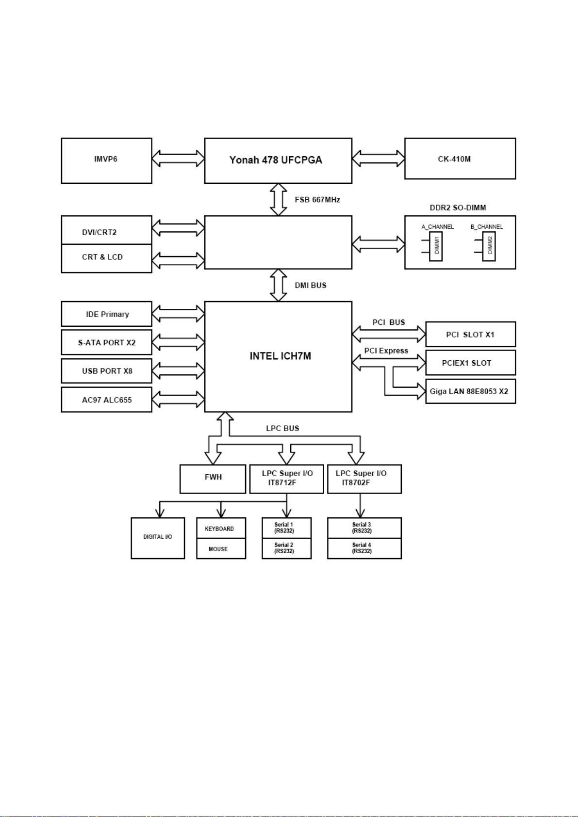
1.4 System Architecture
All of details operating relations are shown in ADE-6050/ADE-6052 system block diagram.
CRT2 for ADE-6052 only
Intel 945GME
ADE-6050 only
12 / 54

1.5 Dimensions
1.5.1 ADE-6050
ADE-6050/ADE-6052 User’s Manual
13 / 54
Unit: mm
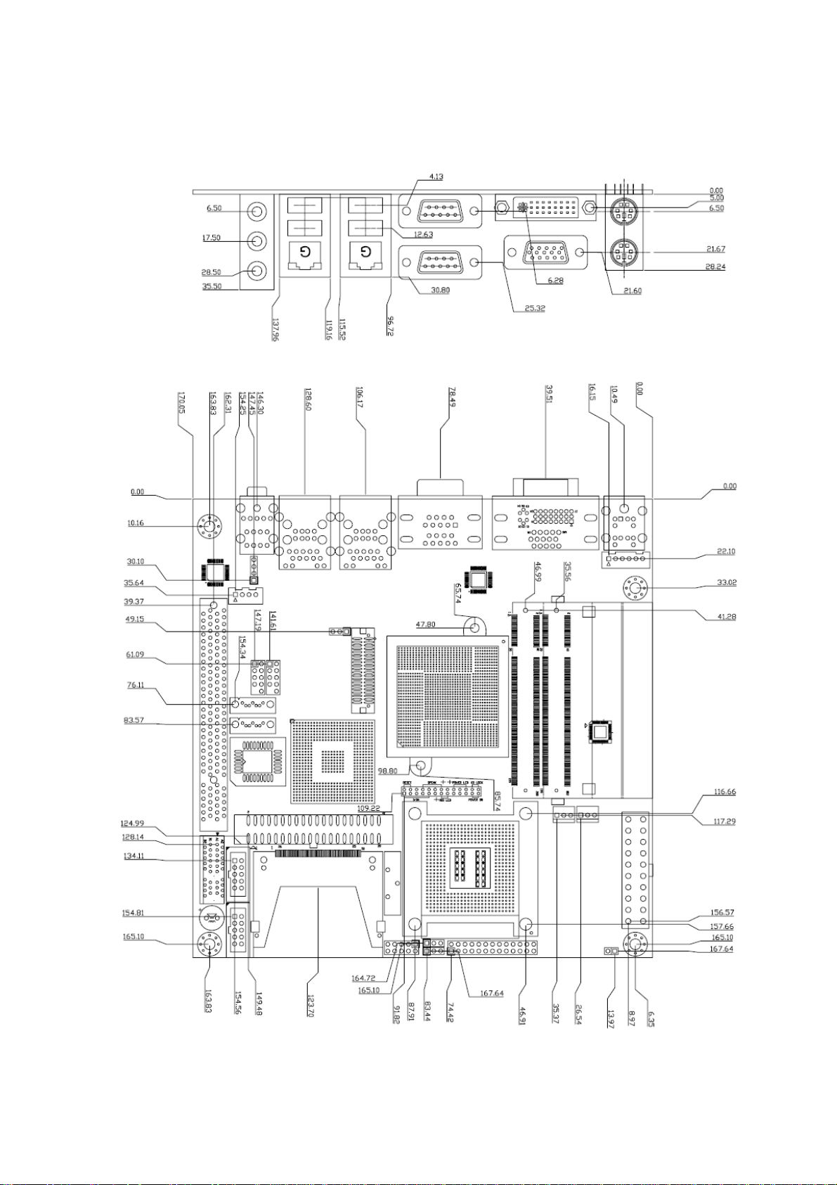
1.5.2 ADE-6052
ADE-6050/ADE-6052 User’s Manual
14 / 54
Unit: mm

ADE-6050/ADE-6052 User’s Manual
CHAPTER 2
15 / 54
ADE-6050/ADE-6052 User’s Manual
2. Hardware Configuration Setting
This chapter gives the definitions and shows the positions of jumpers, headers and
connectors. All of the configuration jumpers on the board are in the proper position. The
default settings shipped from factory are marked with an asterisk ().
In general, jumpers on the board are used to select options for certain features. Some of
the jumpers are designed to be user-configurable, allowing for system enhancement. The
others are for testing purpose only and should not be altered. To select any option, cover
the jumper cap over (SHORT) or remove (NC) it from the jumper pins according to the
following instructions. Here, NC stands for “Not Connect”.
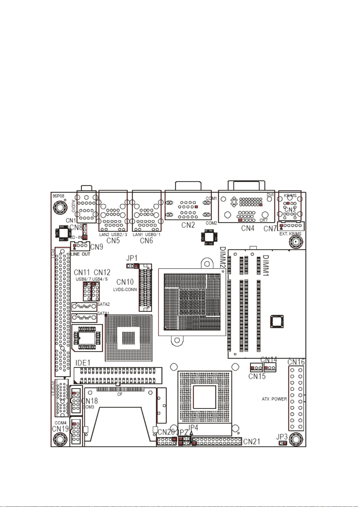
2.1 Board Layout
16 / 54

ADE-6050/ADE-6052 User’s Manual
2.2 Jumpers & Connectors
JUMPERS FUNCTION REMARK
JP1
JP2
JP3
JP4
LVDS power select 1 x 3 header
Clear CMOS select 1 x 3 header
Auto power on select 1 x 2 header
BIOS write protection select 1 x 3 header
CONNECTORS FUNCTION REMARK
CN1
CN2
CN3
CN4
Audio connector
COM1/2 RS232 serial port connectors
PS/2 mouse & keyboard connectors
D-sub 15-pin VGA & DVI connector
(DVI-D for ADE-6050, DVI-I for ADE-6052)
CN5
CN6
CN7
CN8
CN9
USB 2, 3 & LAN 2 connectors
USB 0, 1 & LAN 1 connectors
External keyboard & mouse connector 1 x 6 wafer
CD-In connector 1 x 4 header
Line out connector 1 x 4 wafer
CN10
CN11
CN12
CN14
CN15
CN16
CN18
CN19
CN20
CN21
IDE1
SATA1, SATA2
CFII
DIMM1/2
PCI
PCIEX1
LVDS connector HIROSE
Internal USB connector 6 & 7 2 x 5 header
Internal USB connector 4 & 5 2 x 5 header
System fan connector 1 x 3 wafer
CPU fan connector 1 x 3 wafer
ATX power connector 2 x 10 connector
COM3 RS-232 serial port pin-header 2 x 5 header
COM4 RS-232 serial port pin-header 2 x 5 header
8-bit Digital I/O pin-header (ADE-6050 only) 2 x 5 header
Front panel connector 2 x 13 header
Primary IDE connector 2 x 20 header
Serial A T A1/2 connectors
Type II CompactFlash™ connector
200-pin DDR2 SODIMM sockets
PCI slot
PCI-E by 1 slot
17 / 54

ADE-6050/ADE-6052 User’s Manual
2.3 Jumpers- Setting & Connectors description
2.3.1 LCD power setting select: JP1 2.3.2 Clear CMOS setting select: JP2
PIN No. Description
1-2 3.3V
2-3 5V
PIN No. Description
1-2 Normal operation
2-3 Clear CMOS
2.3.3 Auto power on select: JP3 2.3.4 BIOS write protection setting: JP4
PIN No. Description
1-2 Auto power on
Open Disabled
PIN No. Description
1-2 Write-protection (Default)
2-3 Disable
2.3.5 Audio connector: CN1 2.3.6 COM2/1 RS232 connectors: CN2
PIN No. Description
Blue Line-in
Green Speaker out
Pink MIC-in
PIN No. Description PIN No. Description
1
2
3
4
5
DCD
RXD
TXD
DTR
Ground
6
7
8
9
DSR
RTS
CTS
RI
2.3.7 PS/2 mouse & keyboard connectors: CN3
PS/2 Mouse
PIN No. Description
1 Mouse data
2 NC
3 Ground
4 +5V
5 Mouse clock
6 NC
2.3.8 VGA / DVI Connector: CN4
VGA
PIN No. Description PIN No. Description
1
2
3
4
5
6
7
8
Red Signal
Green Signal
Blue Signal
NC
Ground 13 HSYNC
Ground 14 VSYNC
Ground 15 DCC_CLK
Ground
9
10
11
12
+5V
Ground
NC
DCC_DATA
PS/2 Keyboard
PIN No. Description
1 Keyboard data
2 NC
3 Ground
4 +5V
5 Keyboard clock
6 NC
PIN No. Description PIN No. Description
1
2
3
4
5
6
7
8
9
10
11
12
C1
C2
C3
TDC2#
TDC2
GND
NC
NC
SC_DDC
SD_DDC
NC
TDC1#
TDC1
GND
NC
Red
Green
Blue
DVI-D/DVI-I
13
14
15
16
17
18
19
20
21
22
23
24
C4
C5
NC
DVI_5V
GND
DVI_DET
TDC0#
TDC0
GND
NC
NC
GND
TLC
TLC#
HSYNC
Ground
18 / 54

ADE-6050/ADE-6052 User’s Manual
2.3.9 LAN 1 + USB 0/1 & LAN 2 + USB 2/3 Connectors: CN6 & CN5
LAN 1/2
PIN No. Description PIN No. Description
1 MDI0+ 5 MDI2+
2 MDI0- 6 MDI23 MDI1+ 7 MDI3+
4 MDI1- 8 MDI3-
PIN No. Description PIN No. Description
1 +5 V (fused) 5 +5 V (fused)
2 USBP0-/2- 6 USBP1-/33 USBP0+/2+ 7 USBP1+/3+
4 Ground 8 Ground
USB 0/1/2/3
2.3.10 Internal USB 4/5 & 6/7 Connectors: CN12 & CN11
Description PIN No. PIN No. Description
VCC 1 2 VCC
USBP4-/6- 3 4 USBP5-/7-
USBP4+/6+ 5 6 USBP5+/7+
Ground 7 8 Ground
NC 9 10 NC
Note :
1) If you are using a USB 2.0 device with Windows
2000/XP, you will need to install the USB 2.0 driver
from the Microsoft
pack 1 (or later) for Windows
pack4 (or later) for Windows
to install the driver.
®
website. If you are using Service
®
XP, and using Service
®
2000, you will not have
2.3.11 External K/B & M/S Connector: CN7 2.3.12 CD-In Connector: CN8
PIN No. Description
1 MS Clock
2 MS Data
3 KB Clock
4 KB Data
5 Ground
6 VCC
PIN No. Description
1 CD-L
2 CD-Ground
3 CD-Ground
4 CD-R
19 / 54

ADE-6050/ADE-6052 User’s Manual
2.3.13 Line out Connector: CN9 2.3.14 LVDS Connector: CN10
PIN No. Description
1 LOUT_L
2 Ground
3 Ground
4 LOUT_R
Description PIN. PIN. Description
NC 2 1 NC
Ground 4 3 Ground
LVDS_YAM1 6 5 LVDS_YAM0
LVDS_YAP1 8 7 LVDS_YAP0
Ground 10 9 Ground
LVDS_CLKAM 12 11 LVDS_YAM2
LVDS_CLKAP 14 13 LVDS_YAP2
Ground 16 15 Ground
LVDS_YBM0 18 17 NC0
LVDS_YBP0 20 19 NC
Ground 22 21 Ground
LVDS_YBM2 24 23 LVDS_YBM1
LVDS_YBP2 26 25 LVDS_YBP1
Ground 28 27 Ground
NC 30 29 LVDS_CLKBM
NC 32 31 LVDS_CLKBP
+12V 34 33 NC
+12V 36 35 NC
VCC_LCD 38 37 NC
VCC_LCD 40 39 LCD_BKL
2.3.15 System Fan Connector: CN14 2.3.16 CPU Fan Connector: CN15
PIN No. Description
1 Ground
2 +12V
3 Fan Speed Control
PIN No. Description
1 Ground
2 +12V
3 Fan Speed Control
2.3.17 ATX power Connector: CN16 2.3.18 COM3 / COM4 Connectors: CN18/CN19
PIN No. Description PIN No. Description
1 +3.3V 11
2 +3.3V 12
3 Ground 13
4 +5V 14
5 Ground 15
6 +5V 16
7 Ground 17
8 NC 18
9 5VSB 19
10 +12V 20
+3.3V
-12V
Ground
PS-ON
Ground
Ground
Ground
-5V
+5V
+5V
Description
DCD 1 2 DSR
RXD 3 4 RTS
TXD 5 6 CTS
DTR 7 8 RI
Ground 9 10 VCC
PIN PIN
Description
20 / 54

ADE-6050/ADE-6052 User’s Manual
2.3.19 8-bit Digital I/O Connector: CN20
2.3.20 Front Panel Connector: CN21
(ADE-6050 only)
Description
EXT_VDD 1 2 I1
O1 3 4 I2
O2 5 6 I3
O3 7 8 I4
O4 9 10 EXT_VSS
PIN
No.
PIN
No.
Description
Description PIN PIN Description
IRDA
+5V
NC
IRRX
Ground
IRTX
HDD LED
HDLED+
HDLED-
TB LED
NC
Ground
PW_ON
PWRBT+
PWRBT-
1 2
3 4
5
7 8
9 10
12
13 14
15
18
17 20
19 22
23 24
25 26
RESET
RESET+
RESET-
SPEAKER
SPEAKER
BUZZ
Ground
+5V
PW_ LED
PWLED+
NC
PWLED-
KB_LOCK
KBLOCK
Ground
2.3.21 Primary IDE Connector: IDE1 2.3.22 Serial ATA Connectors: SATA1, SATA2
Description PIN PIN Description
Reset IDE
Host Data 7
Host Data 6
Host Data 5
Host Data 4
Host Data 3
Host Data 2
Host Data 1
Host Data 0
Ground
DRQ 0
Host IOW
Host IOR
IOCHRDY
DACK 0
IRQ 14
Address 1
Address 0
Chip Select 0
Activity
1 2
3 4
5 6
7 8
9 10
11 12
13 14
15 16
17 18
19 20
21 22
23 24
25 26
27 28
29 30
31 32
33 34
35 36
37 38
39 40
Ground
Host Data 8
Host Data 9
Host Data 10
Host Data 11
Host Data 12
Host Data 13
Host Data 14
Host Data 15
--Ground
Ground
Ground
Ground
Ground
NC
Ground
Address 2
Chip Select 1
Ground
PIN No. Description
1
2
3
4
5
6
7
These SATA connectors support Serial AT A II. Each SATA
connector can only support one serial ATA device.
Note: With most storage devices, there is a power cable
that you need attach to a power source (power
supply).
Ground
SATA_TX+
SATA_TX-
Ground
SATA_RX-
SATA_RX+
Ground
21 / 54

ADE-6050/ADE-6052 User’s Manual
CHAPTER 3
22 / 54

ADE-6050/ADE-6052 User’s Manual
3. System Installation
This chapter provides you with instructions on how to setup your system. The additional
information shows you how to install CPU / FAN and memory.
3.1 Socket 478 Processors
3.1.1 Installing CPU
Check and confirm that you are going to install correctly CPU type and pin numbers.
Take the screwdriver and releasing screw-nut of the socket 478.
Rotate mark of screw-nut to face the “OPEN”.
Align the pins of the CPU against the pinholes of the socket 478. Be sure to pay
attention to the orientation of the CPU.
OPEN
Screw Nut
CLOSED
Push down the CPU into the socket 478.
Rotate mark of screw-nut to face the “CLOSED”.
Note: Do not force the CPU into the socket. It may bend the pins and damage the
CPU.
3.2 Installing Cooling Fan
Warning: For a safety landing, avoid leaving prongs on hard surface.
Instructions:Smear thermal grease on the top of the CPU. Lower the CPU fan onto
the CPU/CPU socket and secure it using the attachments or screws
provided on the fan. Finally, attach the fan power cable to the CPUFAN
adapter and be careful not to place the cable on the CPU cooling fan.
23 / 54

ADE-6050/ADE-6052 User’s Manual
3.3 Main Memory
The figures display the notch marks and what they should look like on your SO-DIMM
memory module.
SO-DIMM has 200-pins and two notches, that will match with the onboard SO-DIMM socket.
Memory modules are installed by placing the chip firmly into the socket at a parallel angle
and pressing straight down until it fits tightly into the SO-DIMM socket.
SO-DIMM Memory and 200-pins Socket
Memory Installation
NOTE: For maintaining system stability, do not change any of memory parameters in BIOS
setup to upgrade your system performance without acquiring technical information.
3.4 Installations
To install the board into standard chassis or proprietary environment, you need to perform
the following steps:
1. Check all jumpers setting on proper position
2. Install and configure CPU and memory module on right position
3. Place the board into the dedicated position in your system
4. Attach cables to existing peripheral devices and secure it
24 / 54

ADE-6050/ADE-6052 User’s Manual
CHAPTER 4
25 / 54

ADE-6050/ADE-6052 User’s Manual
4. BIOS Setup
4.1 Entering Setup
PHOENIX-AWARD™ has a built-in setup program that allows users to modify the basic
system configuration. This information is stored in CMOS RAM whose power is supplied by
a battery so that it can retain the setup information even when the power is turned off. Press
the key “Delete” when you Power on or Reboot the computer system. (i.e. After the logo
appears at the center of the screen, please press Delete to enter the BIOS setup program).
In the BIOS, make sure that everything is working fine before you try to optimize it for
maximum performance.
It is possible for the CMOS battery to fail, this will cause data loss in the CMOS only. If this
does happen you will need to reconfigure your BIOS settings.
4.2 Main Menu
When you enter the PHOENIX-AWARD™ CMOS Setup Utility, the Main will appear on the
screen. The Main allows you to select several configuration options. Use the left/right arrow
keys to highlight a particular configuration screen from the top menu bar or use the down
arrow key to access and configure the information below.
26 / 54

4.2.1 Standard CMOS Features
ADE-6050/ADE-6052 User’s Manual
4.2.1.1 Date (mm/date/year):
Set the system date. Note that the ‘Day’ automatically changes when you set the date.
4.2.1.2 Time (hh/mm/ss):
Set the system time.
4.2.1.3 IDE Channel 0 / 1 Master:
Press <Enter> to enter the sub menu of detailed options.
4.2.1.4 IDE Channel 0 / 1 Slave:
Press <Enter> to enter the sub menu of detailed options.
4.2.1.5 SATA Channel 1 / 2:
Press <Enter> to enter the sub menu of detailed options.
4.2.1.6 Video:
It allows you to select the type of displaying standard you are using.
The Choice: EGA/VGA/CGA 40/CGA 80/MONO.
4.2.1.7 Halt On:
Select the situation in which you want the BIOS to stop the POST process and notify you.
The Choice: All Errors/No Errors/All, but Keyboard/All, but Diskette/All, but Disk/Key.
4.2.1.8 Base Memory:
Displays the amount of conventional memory detected during boot up.
4.2.1.9 Extended Memory:
Displays the amount of extended memory detected during boot up.
27 / 54

4.2.1.10 Total Memory:
Displays the total memory available in the system.
ADE-6050/ADE-6052 User’s Manual
28 / 54

4.2.2 Advanced BIOS Features
ADE-6050/ADE-6052 User’s Manual
4.2.2.1 CPU Feature
29 / 54

ADE-6050/ADE-6052 User’s Manual
4.2.2.1.1 Delay Prior to Thermal:
Select this item allows the delay prior to thermal time.
The Choice: Auto, 4, 8, 16, 32Min.
4.2.2.1.2 Execute Disable Bit:
Select when disable, forces the XD feature flag to always return 0.
The choice: Enabled, Disabled.
4.2.2.2 Virus Warning:
Allow you to choose the VIRUS Warning feature for IDE Hard Disk boot sector protection.
If this function is enabled and someone attempts to write data into this area, BIOS will show
a warning message on screen and alarm beep.
The choice: Enabled, Disabled.
4.2.2.3 Hyper-Threading Technology:
When you install a CPU featuring Hyper-Threading Technology, this item will allow you to
enable or disable the Hyper-Threading technology.
The choice: Enabled, Disabled.
4.2.2.4 Quick Power On Self Test
This category speeds up Power On Self Test (POST) after you power up the computer. If
it is set to Enable, BIOS will shorten or skip some check items during POST.
The choice: Enabled, Disabled.
4.2.2.5 Boot Up NumLock Status
Select power on state for NumLock.
The choice: On, Off.
4.2.2.6 Gate A20 Option
Select if chipset or keyboard controller should control GateA20.
The choice: Normal, Fast.
4.2.2.7 Typematic Rate Setting
Keystrokes repeat at a rate determined by the keyboard controller. When enabled, the
typematic rate and typematic delay can be selected.
The choice: Enabled, Disabled.
4.2.2.8 Typematic Rate (Chars/Sec)
Sets the number of times a second to repeat a keystroke when you hold the key down.
The choice: 6, 8, 10, 12, 15, 20, 24 and 30.
4.2.2.9 Typematic Delay (Msec)
Sets the delay time after the key is held down before it begins to repeat the keystroke.
The choice: 250, 500, 750 and 1000.
4.2.2.10 Security Option
Select whether the password is required every time the system boots or only when you
enter setup.
The choice: System, Setup.
30 / 54

ADE-6050/ADE-6052 User’s Manual
4.2.2.11 APIC Mode
This item allows you to enable or disable APIC Mode.
The choice: Enabled, Disabled.
4.2.2.12 MPS Version Control For OS
Select the operating system that is Multi-Processors Version Control for OS.
The choice: 1.4, 1.1.
31 / 54

ADE-6050/ADE-6052 User’s Manual
4.2.2.13 OS Select For DRAM > 64MB
Select the operating system that is running with greater than 64MB of RAM on the system.
The choice: Non-OS2, OS2.
4.2.2.14 Cache Setup
4.2.2.14.1 CPU L1& L2 Cache
These two categories speed up memory access. However, it depends on CPU/chipset
design.
The choice: Enabled, Disabled.
4.2.2.14.2 CPU L3 Cache
The option enables Level 3 cache memory. However, it depends on CPU/chipset design.
The choice: Enabled, Disabled.
32 / 54

4.2.2.15 Boot Seq & Floppy Setup
ADE-6050/ADE-6052 User’s Manual
4.2.2.15.1 Hard Disk Boot Priority
Press Enter and It shows Bootable add-in Card.
4.2.2.15.2 First/Second/Third Boot Device
The BIOS attempts to load the operating system from the devices in the sequence selected
in these items.
The choice: Floppy, LS/ZIP, HDD, SCSI, CDROM, LAN and Disabled.
4.2.2.15.3 Boot Other Device
When enabled, the system searches all other possible locations for an operating system if it
fails to find one in the devices specified under the first, second, and third boot devices.
The Choice: Enabled, Disabled.
4.2.2.15.4 Onboard LAN Boot ROM
Select “Enabled” if your system has a LAN device installed on the system board and you
wish to use it.
The Choice: Enabled, Disabled.
33 / 54

4.2.3 Advanced Chipset Features
ADE-6050/ADE-6052 User’s Manual
For ADE-6050
For ADE-6052
34 / 54

ADE-6050/ADE-6052 User’s Manual
4.2.3.1 DRAM Timing Selectable
Select the operating system that is selecting DRAM timing, so select SPD for setting
SDRAM timing by SPD.
The Choice: Manual, By SPD.
4.2.3.2 CAS Latency Time
When synchronous DRAM is installed, the number of clock cycles of CAS latency depends
on the DRAM timing.
4.2.3.3 DRAM RAS# to CAS# Delay
The system board designer should set the values in this field, depending on the DRAM
installed. Do not change the values in this field unless you change specifications of the
installed DRAM or the installed CPU. This field is locked when “DRAM Ti ming Selectable” is
set to “By SPD” and is automatically determined by the system.
The choice: Auto, 5, 4, 3, 2.
4.2.3.4 DRAM RAS# Precharge
If an insufficient number of cycles are allowed for the RAS to accumulate its charge before
DRAM refresh, the refresh may be incomplete and the DRAM may fail to retain data. Fast
gives faster performance; and Slow gives more stable performance. This field applies
only when synchronous DRAM is installed in the system.
4.2.3.5 Precharge Delay (tRAS)
Select the operating system that is active to precharge delay.
4.2.3.6 System Memory Frequency
You can use this item to select operating frequency for the main system memory.
4.2.3.7 SLP_S4# Assertion Width
The item allows you to select the assertion width of SLP_S4#
The choice: 4 to 5 Sec, 3 to 4 Sec, 2 to 3 Sec, 1 to 2 Sec.
4.2.3.8 System BIOS Cacheable
Selecting “Enabled” allows caching of the system BIOS ROM at F0000h-FFFFFh, resulting
in better system performance. However, if any program writes to this memory area, a
system error may result.
The choice: Enabled, Disabled.
4.2.3.9 Video BIOS Cacheable
Select “Enabled” allows caching of the video BIOS, resulting in better system performance.
However, if any program writes to this memory area, a system error may result.
The choice: Enabled, Disabled.
35 / 54

4.2.3.10 PCI Express Root Port Function
ADE-6050/ADE-6052 User’s Manual
4.2.3.10.1 PCI Express x1 Slot
This item allows you to active PCI Express.
The choice: Auto, Enabled, Disabled.
4.2.3.10.2 PCI-E Compliancy Mode
This item allows you to choose PCI-E Compliancy Mode.
The choice: v1.0a, v1.0.
4.2.3.11 PEG/Onchip VGA Control
This item allows you to control the PEG or on-chip VGA.
The choice: Onchip VGA, PEG Port, Auto.
4.2.3.12 On-Chip Frame Buffer Size
Select this item allows you to control the on-chip frame buffer size.
4.2.3.13 DVMT Mode
This item allows you to select the DVMT mode.
The choice: FIXED, DVMT, BOTH.
4.2.3.14 DVMT/FIXED Memory Size
This item allows you to select the DVMT or FIXED memory size.
4.2.3.15 Boot Display
This item allows you to select the boot display device.
36 / 54

ADE-6050/ADE-6052 User’s Manual
4.2.3.16 Panel Scaling
This item allows you to enable or disable the Scaling function.
The choice: AUTO, ON, OFF.
4.2.3.17 Panel Number
This item allows you to select the panel resolution that will be displayed depending on the
LCD panel (LFP).
37 / 54

4.2.4 Integrated Peripheral
ADE-6050/ADE-6052 User’s Manual
4.2.4.1 Onchip IDE Device
38 / 54

ADE-6050/ADE-6052 User’s Manual
4.2.4.2.1. IDE HDD Block Mode
Block mode is also called block transfer, multiple commands, or multiple sector read/write.
If your IDE hard drive supports block mode (most new drives do), select Enabled for
automatic detection of the optimal number of block read/writes per sector the drive can
support.
The choice: Enabled, Disabled.
4.2.4.2.2. IDE DMA Transfer Access
This item could allows you to enabled/disabled the IDE UDMA transfer function and only
use PIO mode.
The choice: Enabled, Disabled.
4.2.4.2.3. On-Chip Primary/Secondary PCI IDE
The integrated peripheral controller contains an IDE interface with support for two IDE
channels. Select “Enabled” to activate each channel separately.
The choice: Enabled, Disabled.
4.2.4.2.4. IDE Primary/Secondary Master/Slave PIO
The four IDE PIO (Programmed Input/Output) fields let you set a PIO mode (0-4) for each
of the four IDE devices that the onboard IDE interface supports. Modes 0 through 4
provide successively increased performance. In Auto mode, the system automatically
determines the best mode for each device.
The choice: Auto, Mode 0, Mode 1, Mode 2, Mode 3 and Mode 4.
4.2.4.2.5. IDE Primary/Secondary Master/Slave UDMA
Ultra DMA/33 implementation is possible only if your IDE hard drive supports it and the
operating environment includes a DMA driver (Windows 95 OSR2 or a third-party IDE bus
master driver). If your hard drive and your system software both support Ultra DMA/33,
select “Auto” to enable BIOS support.
The choice: Auto, Disabled.
4.2.4.2.6. On-Chip Serial ATA
There are five Serial ATA fields let you set the Serial ATA.
The choice: Disabled---Disabled SATA Controller.
Auto---Auto arrange by BIOS.
SATA Only---SATA is operating in legacy mode.
Combined Mode---PATA and SATA are combined. Max. of 2 IDE drives in each
channel.
Enhanced Mode---Enable both SATA and PATA.
Max. of 4 IDE drives are supported.
39 / 54

4.2.4.2.7. SATA Ports Speed Settings
This item allows you set the SATA Ports Speed.
The choice: Disabled, Force GEN I, Force GEN II.
4.2.4.2.8. PATA IDE Mode
This function allows to select PATA IDE mode.
ADE-6050/ADE-6052 User’s Manual
40 / 54
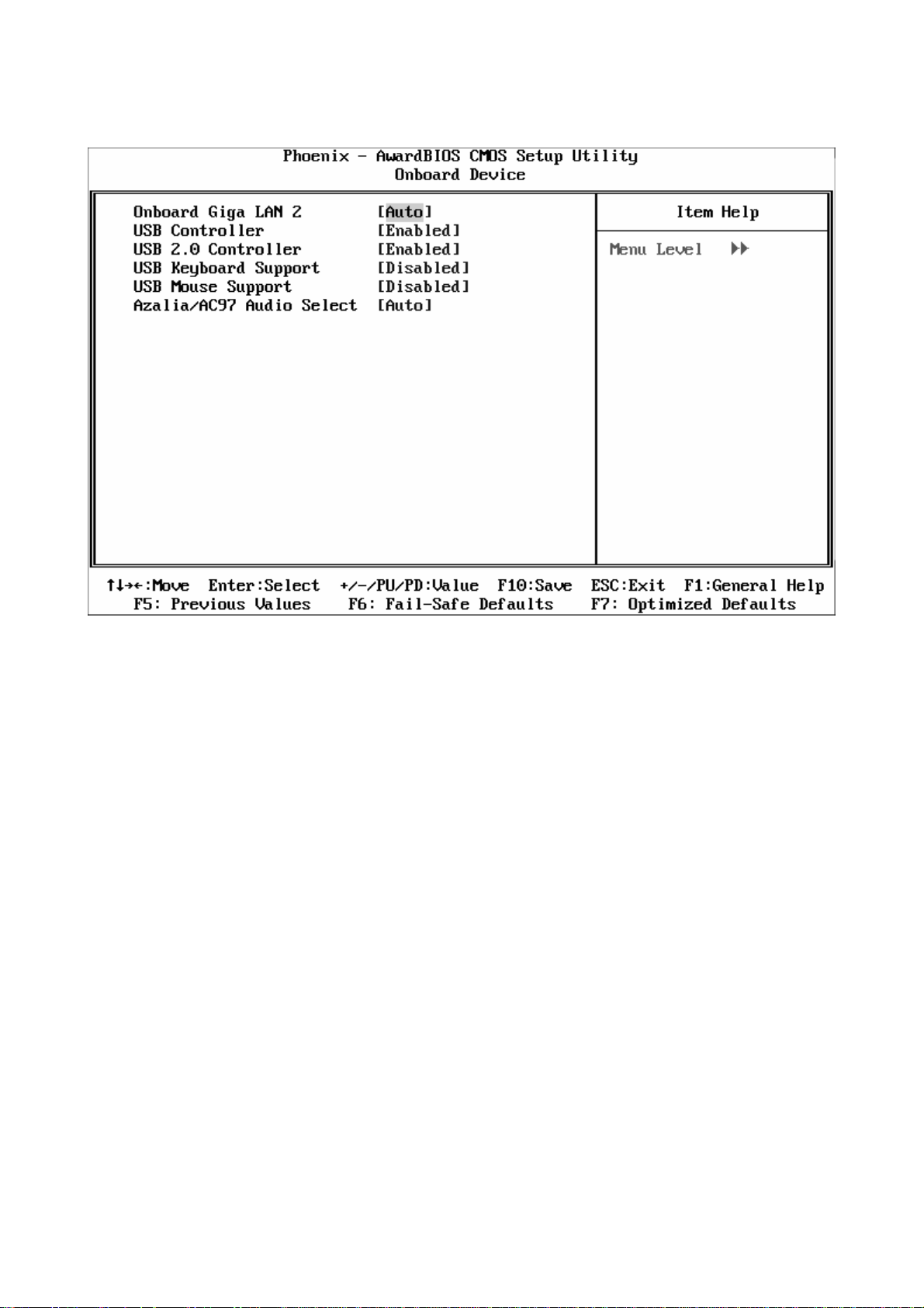
4.2.4.2 Onboard Device
ADE-6050/ADE-6052 User’s Manual
4.2.4.2.1. Onboard Giga Lan 2
Select “Enabled” if your system has a LAN device installed on the system board and you
wish to use it.
The choice: Auto, Enabled, Disabled.
4.2.4.2.2. USB Controller
Select “Enabled” if your system contains a Universal Serial Bus (USB) controller and you
have USB peripherals.
The choice: Enabled, Disabled.
4.2.4.2.3. USB 2.0 Controller
Select “Enabled” if your system contains a Universal Serial Bus 2.0 (USB 2.0) controller
and you have USB peripherals.
The choice: Enabled, Disabled.
4.2.4.2.4. USB Keyboard Support
Select “Enabled” if your system contains a Universal Serial Bus (USB) controller and you
have a USB keyboard.
The choice: Enabled, Disabled.
41 / 54

ADE-6050/ADE-6052 User’s Manual
4.2.4.2.5. USB Mouse Support
Select “Enabled” if your system contains a Universal Serial Bus (USB) controller and you
have a USB mouse.
The choice: Enabled, Disabled.
4.2.4.2.6. Azalia/AC97 Audio Select
This item allows you to select the chipset family to support AC97 Audio
The choice: Auto, Azalia, AC97 Audio only, All disabled.
42 / 54

4.2.4.3 Super IO Device
ADE-6050/ADE-6052 User’s Manual
4.2.4.2.1. Onboard Serial Port 1/2
Select an address and corresponding interrupt for the first and second serial ports.
The choice: 3F8/IRQ4, 2E8/IRQ3, 3E8/IRQ4, 2F8/IRQ3, Disabled and Auto.
4.2.4.2.2. UART Mode Select
This item allows you to determine which Infra Red (IR) function of onboard I/O chip.
The Choice: Normal, IrDA and ASKIR
4.2.4.2.3. UR2 Duplex Mode
Select the value required by the IR device connected to the IR port. Full-duplex mode
permits simultaneous two-direction transmission. Half-duplex mode permits transmission in
one direction only at a time.
The choice: Half, Full.
4.2.4.2.4. PWRON After PWR-Fail
This item allows you to select if you want to power on the system after power failure.
The choice: Off, On and Former-Sts.
43 / 54

4.2.5 Power Management Setup
ADE-6050/ADE-6052 User’s Manual
4.2.5.1 ACPI Function
This function enables PCs to implement Power Management functions through Operating
System and also provides the opportunity to integrated the interface for controlling power
management and Plug-n-Play features on system devices.
4.2.5.2 ACPI Suspend Type
When ACPI function is Enabled, ACPI Suspend Type will be supported S1. In S1 the
computer consumes less power because HDDs and some other devices are powered off,
but CPU is still running and it requires its fan to rotate.
4.2.5.3 Power Management
This category allows you to select the type (or degree) of power saving and is directly
related to the following modes:
1. HDD Power Down, 2. Doze Mode, 3. Suspend Mode
Min. Power Saving: Minimum power management. Doze Mode = 1 hr. Standby Mode =
1 hr., Suspend Mode = 1 hr., and HDD Power Down = 15 min.
Max. Power Saving: Maximum power management -- ONLY AVAILABLE FOR SL
CPU’s. Doze Mode = 1 min., Standby Mode = 1 min., Suspend
Mode = 1 min., and HDD Power Down = 1 min.
User Defined: Allow you to set each mode individually. When not disabled, each of the
ranges is from 1 min. to 1 hr. except for HDD Power Down, which ranges
from 1 min. to 15 min. and disable.
44 / 54

ADE-6050/ADE-6052 User’s Manual
4.2.5.4 Video Off Method
This determines the manner in which the monitor is blanked.
V/H SYNC+Blank: This selection will cause the system to turn off the vertical and
horizontal synchronization ports and write blanks to the video buffer.
Blank Screen: This option only writes blanks to the video buffer.
DPMS: Initial display power management signaling.
4.2.5.5 Video Off In Suspend
This item allows you to on/off Method function.
The choice: Yes, No.
4.2.5.6 Suspend Type
Select the Suspend Type.
The choice: PwrOn Suspend, Stop Grant.
4.2.5.7 Suspend Mode
When “Enabled” and after the set time of system inactivity. All devices except the CPU will
be shut off.
The choice: Disabled, 1, 2, 4, 8, 12, 20, 30, 40 Min and 1Hour.
4.2.5.8 HDD Power Down
When “Enabled” and after the set time of system inactivity, the hard disk drive will be
powered down while all other devices remain active.
The choice: Disabled, 1~15Min.
4.2.5.9 Sort-Off by PWR-BTTN
Pressing the power button for more than 4 seconds forces the system to enter the Soft-Off
state when the system has “hung.
The choice: Delay 4 Sec, Instant-Off.
4.2.5.10 Wake-Up by PCI Card
An input signal from PME on the PCI card awakens the system from a soft off state.
The choice: Enabled, Disabled.
4.2.5.11 Power On by Ring
An input signal on the serial Ring Indicator (RI) line (in other words, an incoming call on the
modem) awakens the system from a soft off state.
The choice: Enabled, Disabled.
4.2.5.12 Resume by Alarm
When “Enabled”, your can set the date and time at which the RTC (real-time clock) alarm
awakens the system from Suspend mode.
The choice: Enabled, Disabled.
4.2.5.13 Primary/Secondary IDE 0/1
This function is for setting IDE 0/1 on primary/secondary mode.
45 / 54

ADE-6050/ADE-6052 User’s Manual
4.2.5.14 FDD,COM,LPT Port
System can be awaked by Floppy Drive, COM or LPT port.
4.2.5.15 PCI PIRQ[A-D]#
This function will cause the system waking up completely from the power management
mode.
46 / 54
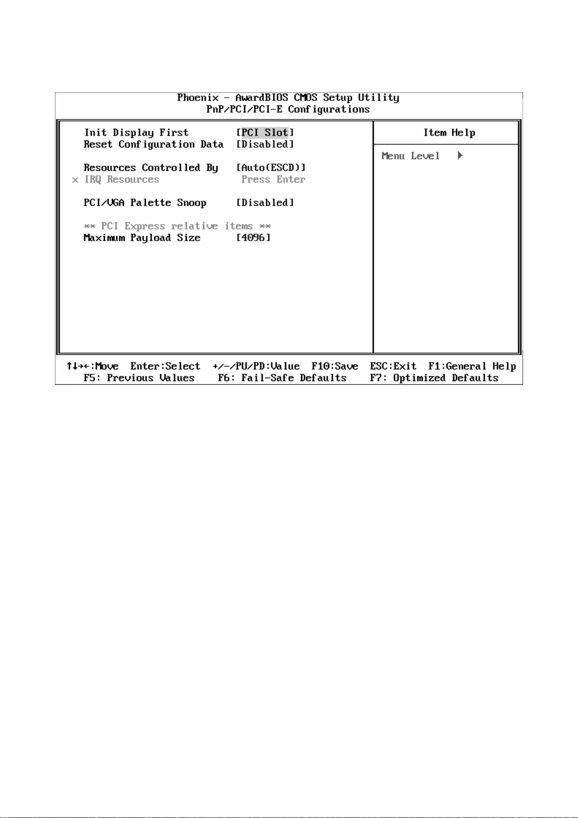
4.2.6 PnP/PCI/PCI-E Configurations
ADE-6050/ADE-6052 User’s Manual
4.2.6.1 Init Display First
This item allows you to decide to active whether PCI Slot or on-chip VGA first.
4.2.6.2 Reset Configuration Data
Normally, you leave this field Disabled. Select “Enabled” to reset Extended System
Configuration Data (ESCD) when you exit Setup if you have installed a new add-on and the
system reconfiguration has caused such a serious conflict that the operating system cannot
boot.
The choice: Enabled, Disabled.
4.2.6.3 Resources Controlled By
The Award Plug and Play BIOS has the capacity to automatically configure all of the boot
and Plug and Play compatible devices. However, this capability means absolutely nothing
unless you are using a Plug and Play operating system such as Windows®95. If you set
this field to “Manual” choose specific resources by going into each of the sub menu that
follows this field.
The choice: Auto (ESCD), Manual.
4.2.6.3.1 IRQ Resources
When resources are controlled manually, assign each system interrupt a type, depending
on the type of device using the DMA channel.
47 / 54

ADE-6050/ADE-6052 User’s Manual
4.2.6.4 PCI/VGA Palette Snoop
This function determines if the graphics card should allow VGA palette snooping by a fixed
function display card. It is only useful if a fixed-function display card using that requires a
VGA-compatible graphics card to be present. Otherwise, leave the setting as default
Disabled.
The choice: Enabled, Disabled.
4.2.6.5 Maximum Payload Size
Set maximum TLP playload size for the PCI Express devices. The unit is byte.
The choice: 128, 256, 512, 1024, 2048, 4096.
48 / 54

4.2.7 PC Health Status
ADE-6050/ADE-6052 User’s Manual
4.2.7.1 VDIMM
The voltage level of the DRAM.
4.2.7.2 Vcore
The voltage level of CPU (Vcore).
4.2.7.3 +3.3V/+5V/+12V/-12V/5Vsb
Show you the voltage of +3.3V/+5V/+12V/-12V.
4.2.7.4 Voltage Battery
Show you the voltage level of the battery.
4.2.7.5 System/CPU Temperature
Show you the current system/CPU temperature.
4.2.7.6 System/CPU FAN Speed
Show you the current System/CPU FAN operating speed.
4.2.8 Load Fail-Safe Default
When you press <Enter> on this item you get a confirmation dialog box with a message
similar to:
Load Fail-Safe Defaults (Y/N)? N
Pressing ‘Y’ loads the BIOS default values for the most stable, minimal-performance
system operations.
49 / 54

ADE-6050/ADE-6052 User’s Manual
4.2.9 Load Optimized Defaults
When you press <Enter> on this item you get a confirmation dialog box with a message
similar to:
Load Optimized Defaults (Y/N)? N
Pressing ‘Y’ loads the default values that are factory settings for optimal performance
system operations.
4.2.10 Supervisor/User Password Setting
You can set either supervisor or user password, or both of then. The differences between
are:
Set Supervisor Password: can enter and change the options of the setup menus.
Set User Password: just can only enter but do not have the right to change the options of
the setup menus. When you select this function, the following message will appear at the
center of the screen to assist you in creating a password.
ENTER PASSWORD:
Type the password, up to eight characters in length, and press <Enter>. The password
typed now will clear any previously entered password from CMOS memory. You will be
asked to confirm the password. Type the password again and press <Enter>. You may
also press <Esc> to abort the selection and not enter a password.
To disable a password, just press <Enter> when you are prompted to enter the password.
A message will confirm the password will be disabled. Once the password is disabled, the
system will boot and you can enter Setup freely.
PASSWORD DISABLED.
When a password has been enabled, you will be prompted to enter it every time you try to
enter Setup. This prevents an unauthorized person from changing any part of your system
configuration.
Additionally, when a password is enabled, you can also require the BIOS to request a
password every time your system is rebooted. This would prevent unauthorized use of
your computer.
You determine when the password is required within the BIOS Features Setup Menu and its
Security option (see Chapter 4). If the Security option is set to “System”, the password will
be required both at boot and at entry to Setup. If set to “Setup”, prompting only occurs
when trying to enter Setup.
50 / 54

ADE-6050/ADE-6052 User’s Manual
4.2.11 Exit Selecting
Save & Exit Setup
Pressing <Enter> on this item asks for confirmation:
Save to CMOS and EXIT (Y/N)? Y
Pressing “Y” stores the selections made in the menus in CMOS – a special section of
memory that stays on after you turn your system off. The next time you boot your
computer, the BIOS configures your system according to the Setup selections stored in
CMOS. After saving the values the system is restarted again.
Exit Without Saving
Pressing <Enter> on this item asks for confirmation:
Quit without saving (Y/N)? Y
This allows you to exit Setup without storing in CMOS any change. The previous
selections remain in effect. This exits the Setup utility and restarts your computer.
51 / 54

ADE-6050/ADE-6052 User’s Manual
Appendix
52 / 54

ADE-6050/ADE-6052 User’s Manual
Appendix A: Watchdog Timer Programming
The Watchdog Timer (WDT) is a special hardware device that monitors the computer
system during normal operation. The WDT has a clock circuit that times down from a set
number to zero. If a monitored item occurs before that timer reaches zero, the WDT resets
and counts down again. If for some reason the monitored item doesn’t occur before the
timer reaches zero, the WDT performs an action, such as a diagnostic operation (rebooting
the computer) or generate an NMI.
53 / 54

ADE-6050/ADE-6052 User’s Manual
Appendix B: GPI/O Programming (ADE-6050 only)
The General Purpose I/O pins are provided for custom system design. The pin
programming as input mode or output mode is depending on the configuration. The pin
definitions are as the following table:
Digital IO Configuration
BIOS
DGIOBASE
Pin No.
DI 2 DGIOBASE + 02h 0
DI 4 DGIOBASE + 02h 1
DI 6 DGIOBASE + 02h 2
DI 8 DGIOBASE + 02h 3
DO 3 DGIOBASE + 01h 0
DO 5 DGIOBASE + 01h 1
DO 7 DGIOBASE + 01h 2
DO 9 DGIOBASE + 01h 3
PIN 1 VCC X
PIN 10 GND X
AWARD
800h
DGIO Port
Data Register
Read/Write: for output port
Pin Bit
Read Only: for input port
Configure pin 3 to output LOW
【C Language】Example:
1. outportb(0x800, 0xFF); // enable dgio
2. iret = inportb(0x801);
3. iret = iret & ~0x01; // set bit0 to 0
4. outportb(0x801, iret); // set pin3 to output low
54 / 54
 Loading...