

Indocomp Systems IND-PM855F User Manual

IND-PM855F
Pentium M
USER’S MANUAL
Version 1.0

ii IND-PM855F User’s Manual
Acknowledgments
Award is a registered trademark of Award Software International,
Inc.
PS/2 is a trademark of International Business Machines
Corporation.
Intel and Celeron are registered trademarks of Intel Corporation.
Microsoft Windows is a registered trademark of Microsoft
Corporation.
Winbond is a registered trademark of Winbond Electronics
Corporation.
IND is registered trademarks of Indocomp Systems Inc.
All other product names or trademarks are properties of their

Copyright Notice
FCC NOTICE
This equipment has been tested and found to comply with the limits for a
Class A digital device, pursuant to part 15 of the FCC Rules. These limits
are designed to provide reasonable protection against harmful
interference when the equipment is operated in a commercial
environment. This equipment generates, uses, and can radiate radio
frequency energy and, if not installed and used in accordance with the
instruction manual, may cause harmful interference to radio
communications. Operation of this equipment in a residential area is
likely to cause harmful interference in which case the user will be
required to correct the interference at his own expense.
You are cautioned that any change or modifications to the equipment not
expressly approve by the party responsible for compliance could void
your authority to operate such equipment.

Contents
TABLE OF CONTENTS
CHAPTER 1 INTRODUCTION
1-1 About This Manual ........................................................ 1-2
1-2 System Specification ...................................................... 1-3
1-3 Extra Industrial Application Features ............................. 1-5
1-4 Safety Precautions …………………………………….. 1-6
CHAPTER 2 HARDWARE CONFIGURATION
2-1 Jumper & Connector Quick Reference Table ................ 2-2
2-2 Component Locations .................................................... 2-3
2-3 How to Set the Jumpers ................................................. 2-4
2-4 COM Port Connector ……..…………………………... 2-6
2-5 RS232/422/485(COM2) Selection ................................ 2-7
2-6 Keyboard or PS/2 Mouse Connector .....................….... 2-8
2-7 Keyboard or PS/2 Mouse Selection .......................….. 2-8
2-8 External Keyboard Connector ....................................... 2-9
2-9 Reset Connector ............................................................ 2-9
2-10 Hard Disk Drive LED Connector .................................. 2-9
2-11 ATX Power Button ….................................................... 2-10
2-12 External Speaker Connector .......................................... 2-10
2-13 Power Led Connector ……............................................ 2-10
2-14 KeyLock Connector ..………………………………… 2-11
2-15 Clear CMOS Data Selection ………………………… 2-11
2-16 CPU Fan Connector ………………………………….. 2-12
2-17 System Fan Connector ………………………………… 2-12
2-18 VGA CRT Connector ………………………………… 2-13
2-19 Hard Disk Drive Connector ........................................... 2-14
2-20 Floppy Disk Drive Connector ....................................... 2-16
2-21 Printer Connector .......................................................... 2-17
2-22 Universal Serial Bus Connector ……………………… 2-18
2-23 IrDA Connector ………………………………………. 2-19
2-24 LAN Connector ………………………………………. 2-20
2-25 GigaLAN (LAN2) Enable/Disable Selection ………… 2-22
2-26 ATX Power Connector ……………………………….. 2-23
2-27 5VSB Connector ……….……………………….…… 2-24
2-28 Memory Installation ………………………………….. 2-24

Contents
2-29 Reset / NMI / Clear Watchdog Selection ..…................. 2-25
2-31 Sound Connector ……………………………….…….. 2-26
2-31 CD Audio-in Connector ………………………………. 2-26
2-32 CF Card Master/Slave Selection ……………………… 2-27
2-33 AT/ATX Power Selection ……………..…………….. 2-28
2-34 ATX Power Selection ………………..……………… 2-29
2-35 Digital I/O Connector ………………………………… 2-30
2-36 LVDS Connector ……………………………………… 2-31
2-37 LVDS Panel Voltage Selection ………………………. 2-32
2-38 Inverter Connector ……………………………………. 2-32
2-39 DVO Connector ……………………………………….. 2-33
CHAPTER 3 SOFTWARE UTILITIES
3-1 Introduction …………..........................................…....... 3-2
3-2 VGA Driver Utility ……………………………….…… 3-3
3-3 Flash BIOS Update ..............................................…....... 3-4
3-4 LAN Driver Utility …...........................................…...... 3-6
3-5 Sound Driver Utility …………………………………… 3-7
3-6 Intel Chipset Software Installation Utility …..……..….. 3-8
3-7 USB2.0 Software Installation Utility ………………….. 3-9
3-8 Watchdog Timer Configuration .................................... 3-10
CHAPTER 4 AWARD BIOS SETUP
4-1 Introduction ................................................................... 4-2
4-2 Entering Setup ............................................................... 4-3
4-3 The Standard CMOS Features ………............................ 4-4
4-4 The Advanced BIOS Features ....................................... 4-8
4-5 Advanced Chipset Features ........................................... 4-11
4-6 Integrated Peripherals …............................................... 4-13
4-7 Power Management Setup ............................................. 4-18
4-8 PNP/PCI Configuration …............................................. 4-21
4-9 PC Health Status …….................................................... 4-23
4-10 Frequency Control ....................................…………...... 4-24
4-11 Load Fail-Safe Defaults ................................................. 4-25
4-12 Load Optimized Defaults .........................................…. 4-25
4-13 Password Setting ……………………………………… 4-26
4-14 Save & Exit Setup ......................................................... 4-27
4-15 Exit Without Saving ………………………………… 4-28

Contents
APPENDIX A EXPANSION BUS
ISA Bus Pin Assignment …………………………………….. A-2
PCI Bus Pin Assignment ..............................................…......... A-3
EPCI Connector ..........................………....................….......... A-4
Compact Flash Card Pin Assignment ………………………… A-5
APPENDIX B TECHNICAL SUMMARY
Block Diagram ........................................................................... B-2
Interrupt Map ............................................................................ B-3
RTC & CMOS RAM Map ........................................................ B-4
Timer & DMA Channels Map .................................................. B-5
I/O & Memory Map ...............................................…................ B-6

Page:1-1
INTRODUCTION
This chapter gives you the information for IND-PM855F. It also
outlines the System specification.
Section includes:
z About This Manual
z System Specifications
z Extra Industrial Application Features
z Safety precautions
Experienced users can skip to chapter 2 on page 2-1
for Quick Start.
CHAPTER
1

Chapter 1 Introduction
Page: 1-2
IND-PM855F USER
′
S MANUAL
1-1. ABOUT THIS MANUAL
Thank you for purchasing our IND-PM855F Socket 478 Pentium M Full Size
Card enhanced with VGA / Sound/ 2LAN, which is fully PC / AT compatible.
IND-PM855F provides faster processing speed, greater expandability and can
handle more task than before. This manual is designed to assist you how to
install and set up the system. It contains four chapters. The user can apply this
manual for configuration according to the following chapters :
Chapter 1 Introduction
This chapter introduces you to the background of this manual, and the
specification for this system. Final part of this chapter will indicate you how
to avoid damaging this Embedded Card.
Chapter 2 Hardware Configuration
This chapter outlines the component location and their functions. In the end of
this chapter, you will learn how to set jumper and how to config ure this card
to meet your own needs.
Chapter 3 Software Utilities
This chapter contains helpful information for proper installations of the VGA
utility, LAN utility, sound utility, and BIOS update. It also describes the
Watchdog timer configuration.
Chapter 4 Award BIOS Setup
This chapter indicates you how to set up the BIOS configurations.
Appendix A Expansion Bus
This Appendix introduces you the expansion bus for ISA/PCI Bus and EPCI
Bus.
Appendix B Technical Summary
This section gives you the information about the Technical maps.

Chapter 1 Introduction
IND-PM855F USER′S MANUAL
Page: 1-3
1-2. SYSTEM SPECIFICATION
z CPU (mPGA 478) :
Intel® Pentium® M processor in mPGA478 socket
Available at 1.3~ 1.8GHz
System bus frequency at 400MHz
Auto detect voltage regulator
z SYSTEM CHIPSET :
Intel® 855GME chipset
z MEMORY :
Supports up to 2GB DDR SDRAM.
Two 184-pin DDR DIMM sockets on board
z CACHE :
Built-in CPU
z REAL-TIME CLOCK / CALENDAR :
256-byte battery backed CMOS RAM.
Hardware implementation to indicate century rollover
z BIOS :
Phoenix-AwardBIOS™ for plug & play function
Memory size with 4 MB, with VGA BIOS
z KEYBOARD/MOUSE CONNECTOR :
Mini DIN connector, selectable for Keyboard, PS/2 Mouse, or Y-Cable
One additional 5-pin External keyboard connector
z UNIVERSAL SERIAL BUS :
Universal Serial Bus Connector on board
Supports up to four USB 2.0 ports.
z BUS SUPPORT :
One ISA/PCI Bus
One External EPCI Bus
One Compact Flash Bus.

Chapter 1 Introduction
Page: 1-4
IND-PM855F USER
′
S MANUAL
z DISPLAY :
Integrated Graphic in Intel® 855GME.
Support D-Sub 15 pin VGA.
Support 18/24bit LVDS connector.
Support 3.3V/5V LVDS Panel Power Selection.
Support 12V Panel Backlight.
* 24bit hardware is ready but Intel® does not recommend using.
Support DVO1 connector.
z IDE INTERFACE :
Two IDE ports support up to four IDE devices.
Supports UDMA 33/66/100.
Compact Flash is connected at secondary IDE Bus.
Compact Flash Master/Slave Mode Selectable.
z FLOPPY DISK DRIVER INTERFACE :
Supports up to two Floppy Disk Drives, 3.5" and 5.25".
z LAN INTERFACE :
Dual ports.
LAN 1: Intel® 82562ET 10/100 Mbps Ethernet.
LAN 2: Intel® 82541PI (10/100/1000).
Supports Wake-on-LAN with ATX power.
z SOUND PORT:
AC ’97 Codec. Realtek ALC202A.
z SERIAL PORT :
Two high speed 16550 Compatible UARTs with Send / Receive 16 Byte
FIFOs. COM1 for RS232; COM2 for RS232/422/485.
z PARALLEL PORT :
One port supports SPP / ECP / EPP Function.
z HARDWARE MONITORING FUNCTION :
Monitor Voltage, CPU Temperature and Cooling Fan.
z IRDA PORT :
One 5-pin Infrared connector
Supports IrDA v1.0 SIR protocol.

Chapter 1 Introduction
IND-PM855F USER′S MANUAL
Page: 1-5
z LED INDICATOR :
HDD LED, Power LED.
z OPERATING TEMPERATURE :
0 to 60°C (32°F to 140°F)
z INPUT POWER REQUIREMENT :
ATX power: +5V, +12V, -12V, 5VSB.
AT power: +5V, +12V, -12V.
z BOARD DIMENSION :
338.5mm x 122mm (13.33” x 4.8”)
z BOARD NET WEIGHT :
370 grams (0.82 lb)
1-3. EXTRA INDUSTRIAL APPLICATION FEATURES
z WATCHDOG TIMER:
Watchdog Timer controllable by software, customer application 1~255
second watchdog timer time-out value.
Reset upon Mouse/Keyboard, SMI or System Reset.
z DIGITAL I/O PORT:
4 bit input and 4 bit output digital port availability.
Decoding address at I/O 400H.
General purpose and Input/Output buffer embedded.

Chapter 1 Introduction
Page: 1-6
IND-PM855F USER
′
S MANUAL
1-4. SAFETY PRECAUTIONS
Follow the messages below to avoid your systems from damage:
1. Avoid your system from static electricity on all occasions.
2. Prevent electric shock. Don‘t touch any components of this card when the card
is power-on. Always disconnect power when the system is not in use.
3. Disconnect power when you change any hardware devices. For instance, when
you connect a jumper or install any cards, a surge of power may damage the
electronic components or the whole system.

Page 2-1
HARDWARE
CONFIGURATION
** QUICK START **
CHAPTER
2
Helpful information describes the jumper & connector settings, and
component locations.
Section includes:
z Jumper & Connector Quick Reference Table
z Component Locations
z Configuration and Jumper settings
z Connector’s Pin Assignments

Chapter 2 Hardware Configuration
Page: 2-2
IND-PM855F USER
′
S MANUAL
2-1. JUMPER & CONNECTOR QUICK REFERENCE TABLE
COM Port Connector ....................…..................………
COM1, COM2
RS232/422/485 (COM2) Selection .....................………
JP2
Keyboard/Mouse Connector ..........….....………………
DIN1
Keyboard/Mouse Selection .........….......……………
JP16
External Keyboard Connector …………………………
EXKB1
Reset Connector .........................…....................……….
JPANEL1 (13,15)
Hard Disk Drive LED Connector .......................……….
JPANEL1 (9,11)
ATX Power Button ……………………………………..
JPANEL1 (14,16)
External Speaker Connector ....…........................………
JPANEL1 (1,3,5,7)
Power LED Connector …………….…...............………
JPANEL1 (8,10,12)
KeyLock Connector …………………………………….
JPANEL1 (17,18)
Clear CMOS Data Selection ……………………………
JP13
CPU Fan Connector ……………………………………
JCFAN1
System Fan Connector ………………………………….
JSFAN1
VGA Connector …................……..……………………
VGA1
Hard Disk Drive Connector …..............…….........…….
IDE1, IDE2
Floppy Disk Drive Connector ….............…….......…….
FDD1
Printer Connector …........................…...…….........……
LPT1
Universal Serial Bus Connector …........................…..…
USB1, USB2
IrDA Connector ………………………………………..
IRDA1, JPANEL1 (21-24)
LAN Connector …....................................……....……...
LAN1, LAN2
GigaLAN (LAN2) Enable/Disable Selection …………..
JP9
ATX Power Connector …………………………………
JATXPWR1
5VSB Connector ………………………………………
JP6
Memory Installation ..................................…......………
DIM1, DIM2
Reset/NMI Selection .………….……………………….
JP18
Sound Connector ………………………….……………
JP4
CD Audio-In Connector ………………………………..
JCDIN1, JCDIN2
Compact Flash Card Master/Slave Selection …………..
JP5
AT/ATX Power Selection ……………………………..
JP14
ATX Power Selection ………………………………….
JP15
Digital I/O Connector ………………………………….
DIO1
LVDS Connector ………………………………………
J2
LVDS Voltage Selection ………………………………
JP7
Inverter Connector ……………………………………
J3
DVO Connector ……………………………………….
DVO1
Chapter 2 Hardware Configuration
IND-PM855F USER′S MANUAL
Page: 2-3
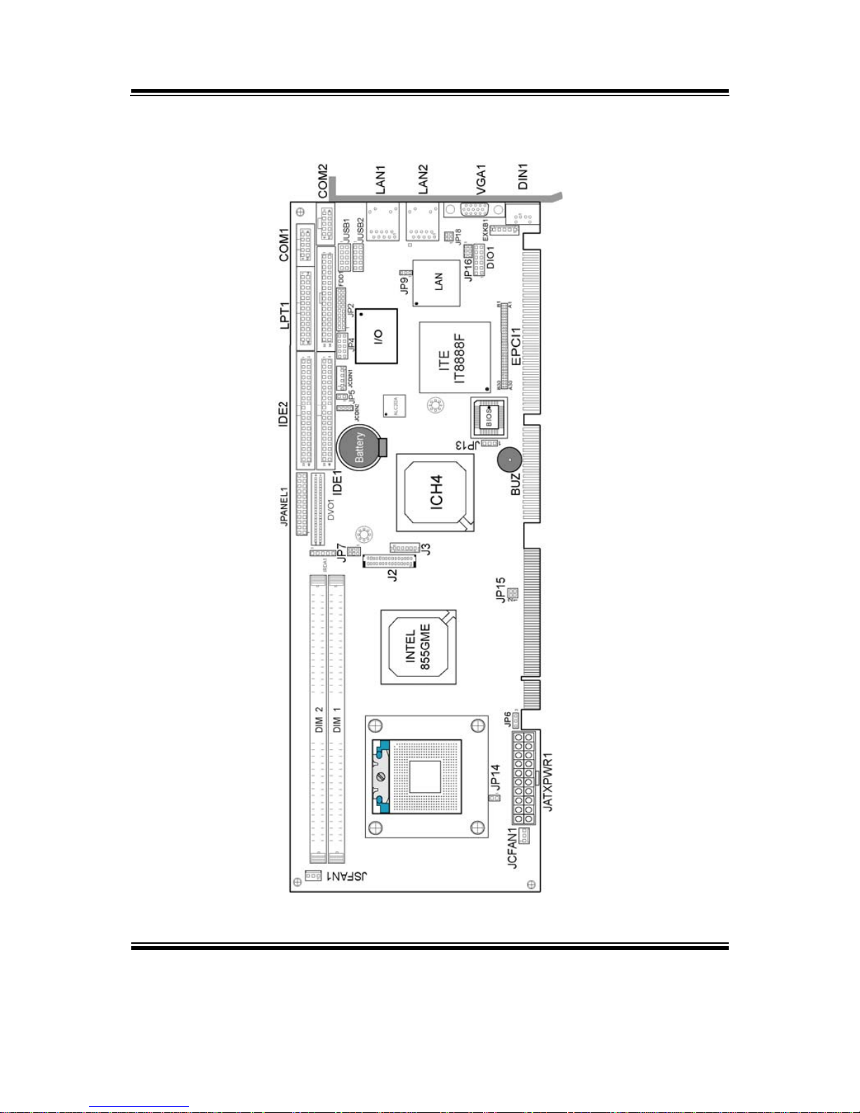
2-2. COMPONENT LOCATIONS
IND-PM855F Connector, Jumper and Component locations

Chapter 2 Hardware Configuration
Page: 2-4
IND-PM855F USER MANUAL
2-3. HOW TO SET THE JUMPERS
You can configure your board by setting jumpers. Jumper is consists of
two or three metal pins with a plastic base mounted on the card, and by
using a small plastic "cap", Also known as the jumper cap (with a metal
contact inside), you are able to connect the pins. So you can set-up your
hardware configuration by "open" or "close" pins.
The jumper can be combined into sets that called jumper blocks. When the
jumpers are all in the block, you have to put them together to set up the
hardware configuration. The figure below shows how this looks like.
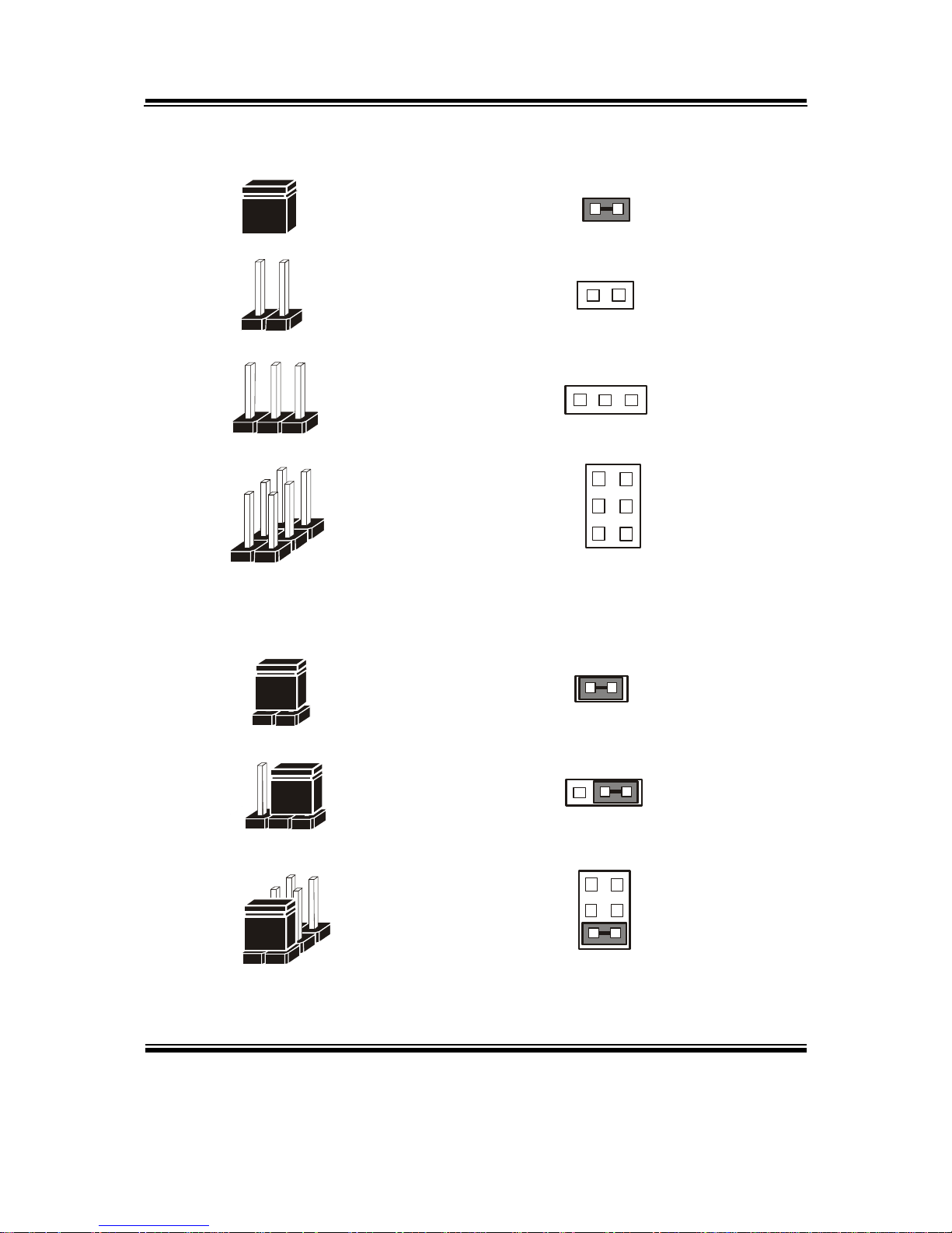
JUMPERS AND CAPS
If a jumper has three pins (for examples, labelled PIN1, PIN2, and PIN3),
You can connect PIN1 & PIN2 to create one setting and shorting. You can
either connect PIN2 & PIN3 to create another setting. The same jumper
diagrams are applied all through this manual. The figure below shows what
the manual diagrams look and what they represent.
Chapter 2 Hardware Configuration
IND-PM855F USER′S MANUAL
Page: 2-5
JUMPER DIAGRAMS
2 pin Jumper
looks like this
Jumper Ca p
looks like this
3 pin Jumper
looks like this
Jumper Bl o ck
looks like this
JUMPER SETTINGS
Looks like this
3 pin Jumper
2-3 pin close(ena b led)
Looks like this
Jumper Block
1-2 pin close(ena b led)
2 pin Jumper close(enabled)
1
1
1
2
12
1
1
Looks like this
Chapter 2 Hardware Configuration
Page: 2-6
IND-PM866F USER
′
S MANUAL
2-4. COM PORT CONNECTOR
COM1 : COM1 Connector
COM1 is fixed as RS-232.
The pin assignment is as follows :
PIN ASSIGNMENT
1 COM1_DCD
2 COM1_RXD
3 COM1_TXD
4 COM1_DTR
5 GND
6 COM1_DSR
7 COM1_RTS
8 COM1_CTS
9 COM1_RI
10 NC
COM2 : COM2 Connector
The COM2 is selectable as RS-232/422/485.
The pin assignment is as follows :
ASSIGNMENT
PIN
RS-232 RS-422 RS-485
1 COM2_DCD TX- TX2 COM2_RXD TX+ TX+
3 COM2_TXD RX+ RX+
4 COM2_DTR RX- RX5 GND GND GND
6 COM2_DSR RTS- NC
7 COM2_RTS RTS+ NC
8 COM2_CTS CTS+ NC
9 COM2_RI CTS- NC
10 NC NC NC
1
6
5
10
COM2
1
6
5
10
COM1
Chapter 2 Hardware Configuration
IND-PM855F USER′S MANUAL
Page: 2-7
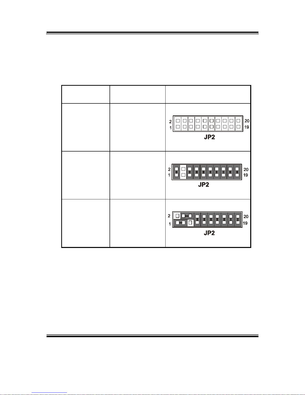
2-5. RS232/422/485 (COM2) SELECTION
JP2 : RS-232/422/485 (COM2) Selection
This connector is used to set the COM2 function.
The jumper settings are as follows :
COM 2
Function
Jumper Settings
(pin closed)
Jumper
Illustrations
RS-232
Open
RS-422
1-2, 5-6, 7-8
9-10, 11-12, 13-14
15-16, 17-18, 19-20
RS-485
1-3, 4-6, 7-8, 9-10
11-12, 13-14, 15-16
17-18, 19-20
*** Manufactory default --- RS-232.
Chapter 2 Hardware Configuration
Page: 2-8
IND-PM855 USER
′
S MANUAL
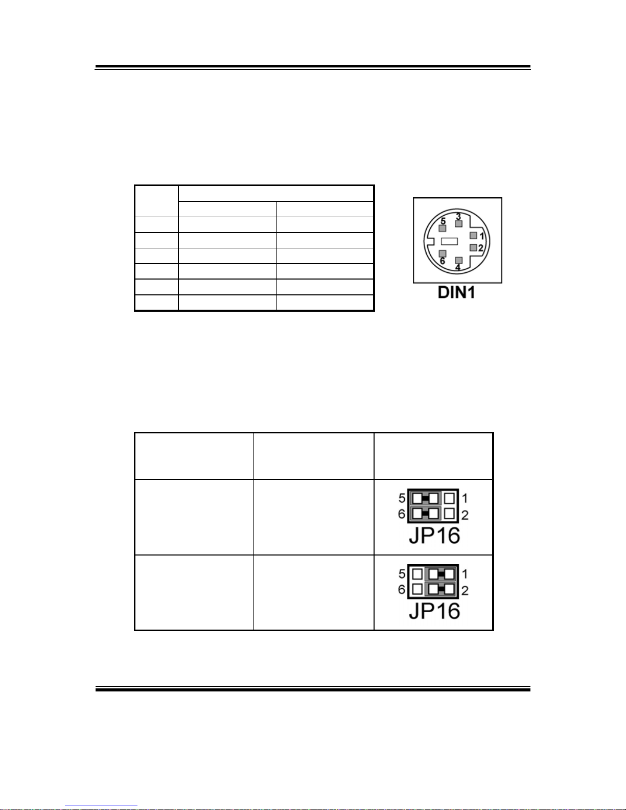
2-6. KEYBOARD OR PS/2 MOUSE CONNECTOR
DIN1 : Keyboard or PS/2 Mouse Connector
DIN connector can support keyboard, Y-cable, or PS/2 Mouse, user may
select the right device to used on “Keyboard or PS/2 Mouse Selection”.
The pin assignments are as follows :
ASSIGNMENT
PIN
Keyboard PS/2 Mouse
1 KBDATA MSDATA
2 MSDATA MSDATA
3 GND GND
4 5VSB 5VSB
5 KBCLK MSCLK
6 MSCLK MSCLK
2-7. KEYBOARD OR PS/2 MOUSE SELECTION
JP16 : Keyboard or PS/2 Mouse Selection
For Y-Cable user, please set the jumper same as AT keyboard.
The jumper settings are as follows:
DEVICE
TYPE
JUMPER SETTING
(pin closed)
JUMPER
ILLUSTRATION
AT KEYBOARD
3-5
4-6
PS/2 MOUSE
1-3
2-4
*** Manufactory default -- AT Keyboard
Chapter 2 Hardware Configuration
IND-PM855F USER′S MANUAL
Page: 2-9
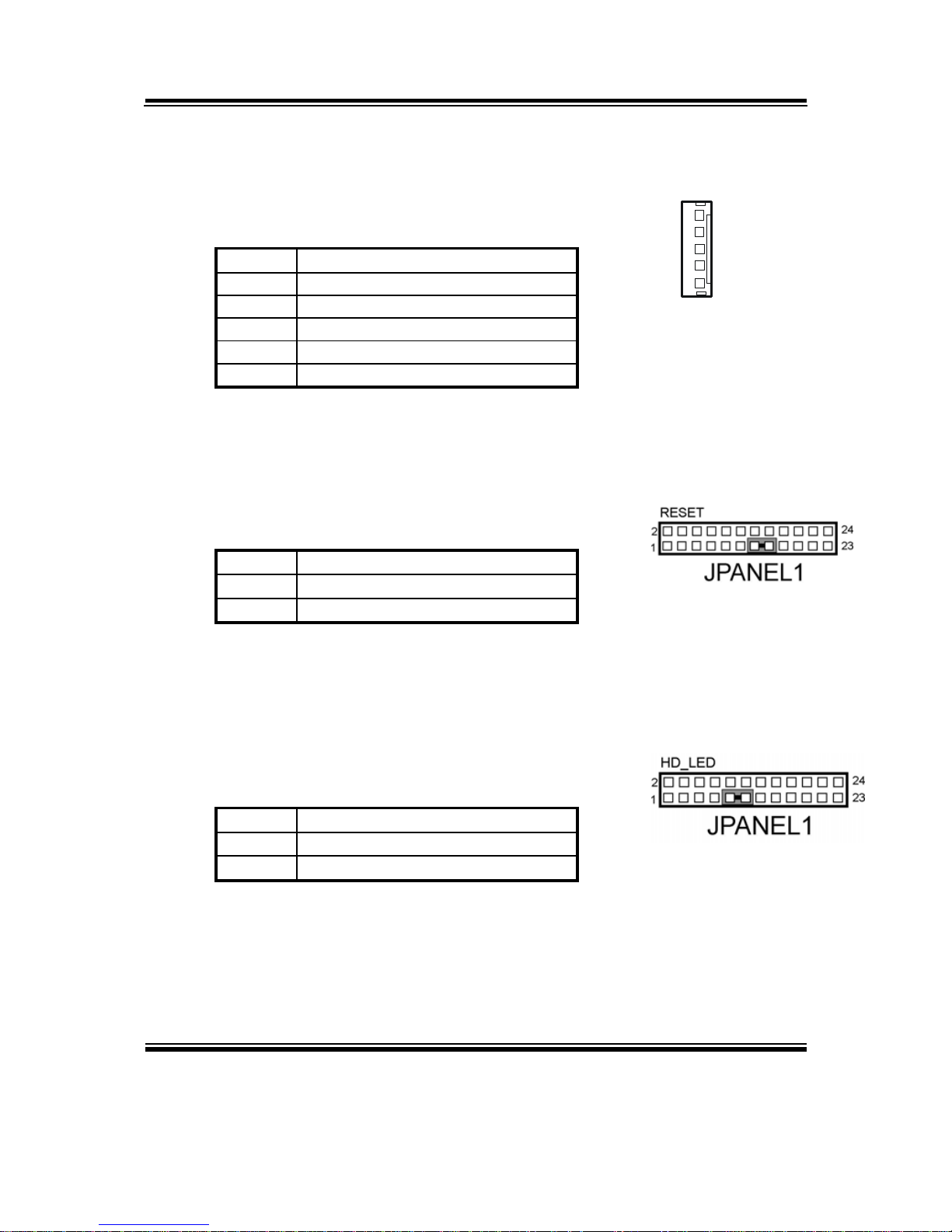
2-8. EXTERNAL KEYBOARD CONNECTOR
EXKB1 : External Keyboard Connector
The pin assignment is as follows :
PIN ASSIGNMENT
1 5VSB
2 GND
3
N
C
4 KDAT
5 KCLK
2-9. RESET CONNECTOR
JPANEL1 (13,15) : Reset Connector.
The pin assignment is as follows :
PIN ASSIGNMENT
13 GND
15 RST_SW
2-10. HARD DISK DRIVE LED CONNECTOR
JPANEL1 (9,11) : Hard Disk Drive LED Connector
The pin assignment is as follows :
PIN ASSIGNMENT
9 PULL-HIGH TO VCC3_3
11 HD_LED
1
EXKB1
Chapter 2 Hardware Configuration
Page: 2-10
IND-PM855F USER
′
S MANUAL
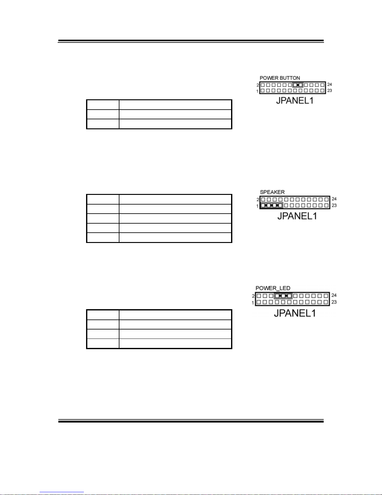
2-11. ATX POWER BUTTON
JPANEL1 (14,16) : ATX Power Button
The pin assignment is as follows :
PIN ASSIGNMENT
14 PULL-HIGH TO 5VSB
16 PWB_SIOJ
2-12. EXTERNAL SPEAKER CONNECTOR
JPANEL1 (1,3,5,7) : External Speaker Connector
The pin assignment is as follows :
PIN ASSIGNMENT
1 SPK3
3 NC
5 NC
7 PULL-HIGH TO VCC
2-13. POWER LED CONNECTOR
JPANEL1 (8,10,12) : Power LED Connector
The pin assignment is as follows:
PIN ASSIGNMENT
8 PULL-HIGH TO VCC
10 PULL-HIGH TO VCC
12 GND
Chapter 2 Hardware Configuration
IND-PM855F USER′S MANUAL
Page: 2-11
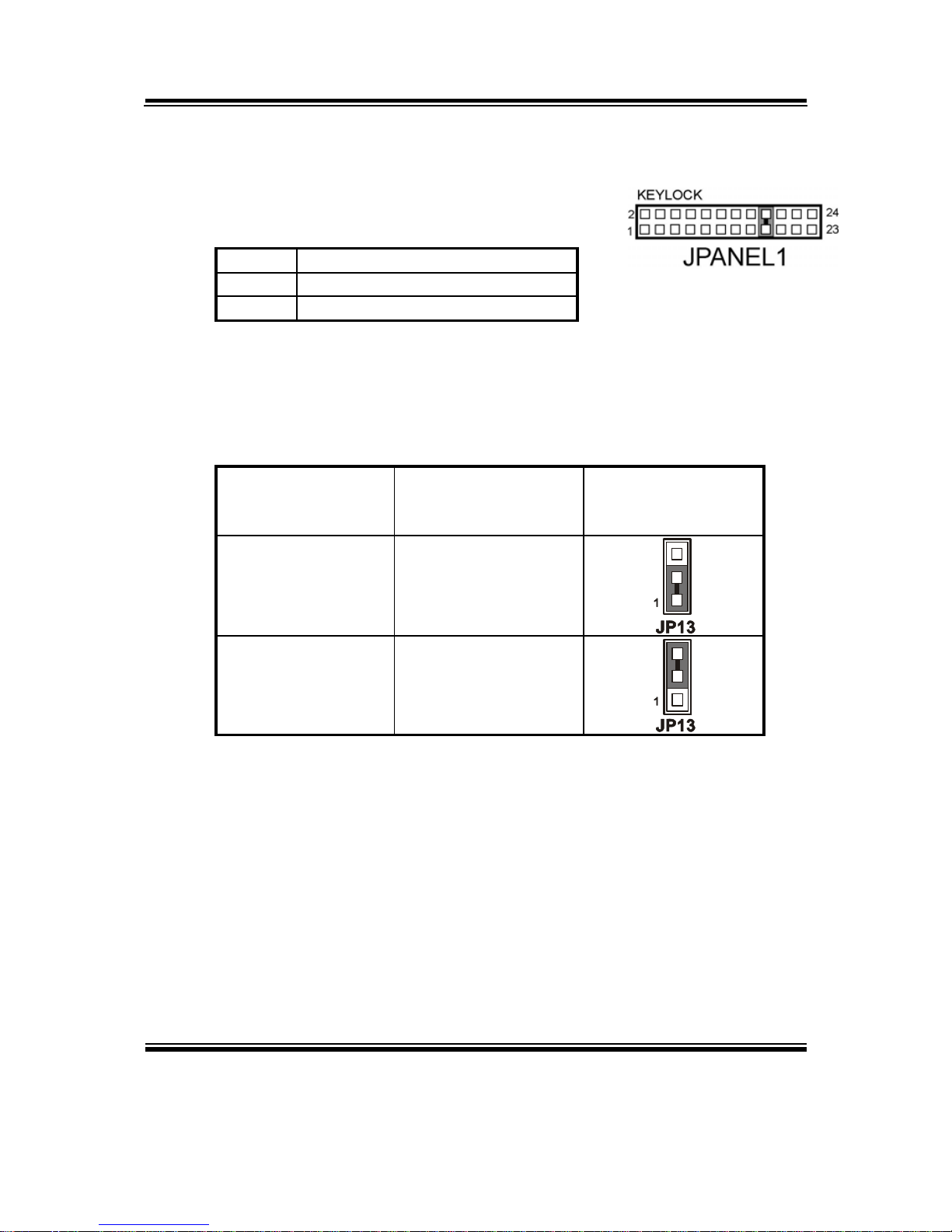
2-14. KEYLOCK CONNECTOR
JPANEL1 (17,18) : Keylock Connector
The pin assignment is as follows:
PIN ASSIGNMENT
17 KEYLOCK
18 GND
2-15. CLEAR CMOS DATA SELECTION
JP13 : Clear CMOS Data Selection
The selections are as follows :
FUNCTION
JUMPER SETTING
(pin closed)
JUMPER
ILLUSTRATION
Normal 1-2
Clear CMOS 2-3
*** Manufacturing Default is set as Normal.
Note: To clear CMOS data, user must power-off the computer and set the jumper to
“Clear CMOS” as illustrated above. After five to six seconds, set the jumper
back to “Normal” and power-on the computer.
Chapter 2 Hardware Configuration
Page: 2-12
IND-PM855F USER
′
S MANUAL
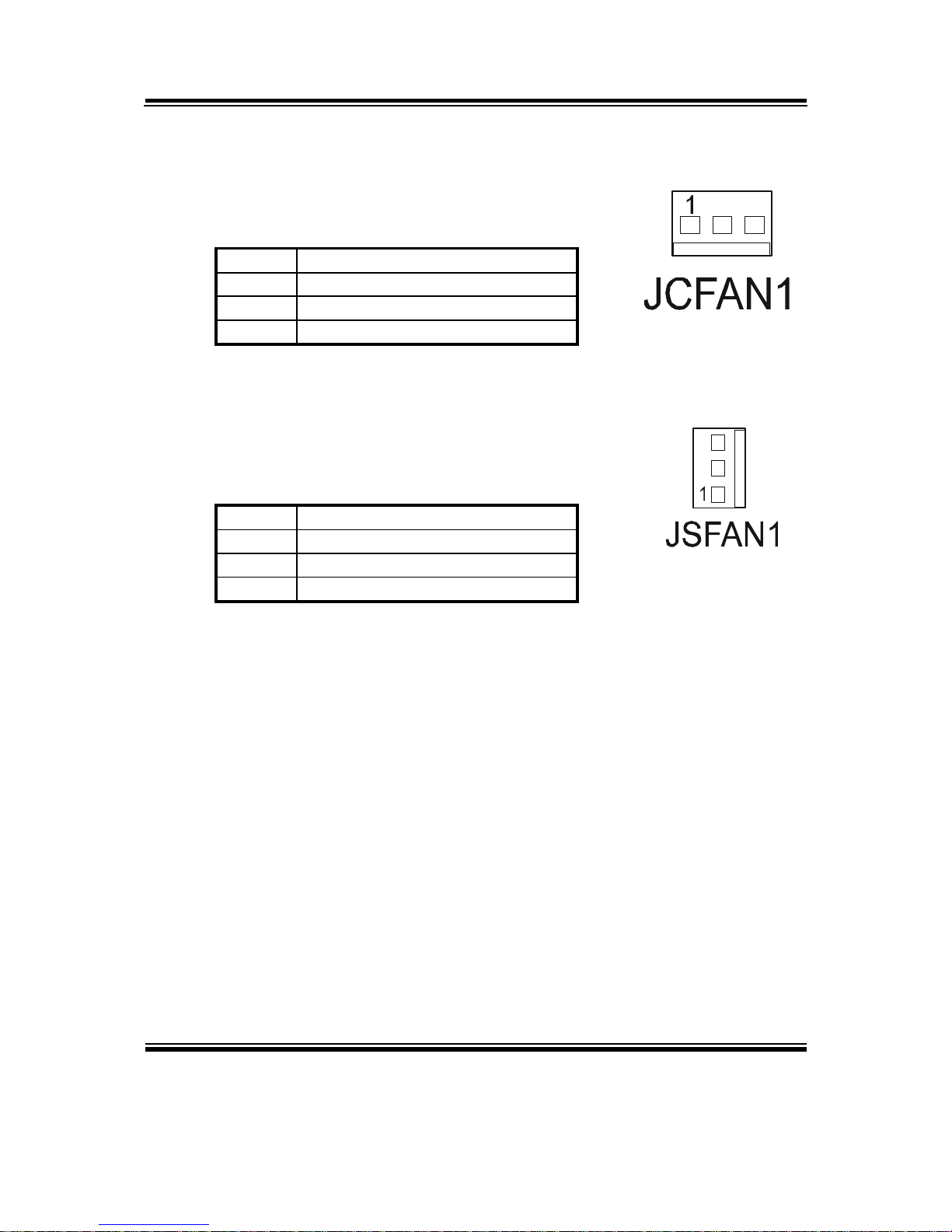
2-16. CPU FAN CONNECTOR
JCFAN1 : CPU Fan connector
The pin assignment is as follows:
PIN ASSIGNMENT
1 GND
2 +12V
3 FAN1
2-17. SYSTEM FAN CONNECTOR
JSFAN1 : System Fan connector
The pin assignment is as follows:
PIN ASSIGNMENT
1 GND
2 +12V
3 FAN0
Chapter 2 Hardware Configuration
IND-PM855F USER′S MANUAL
Page: 2-13
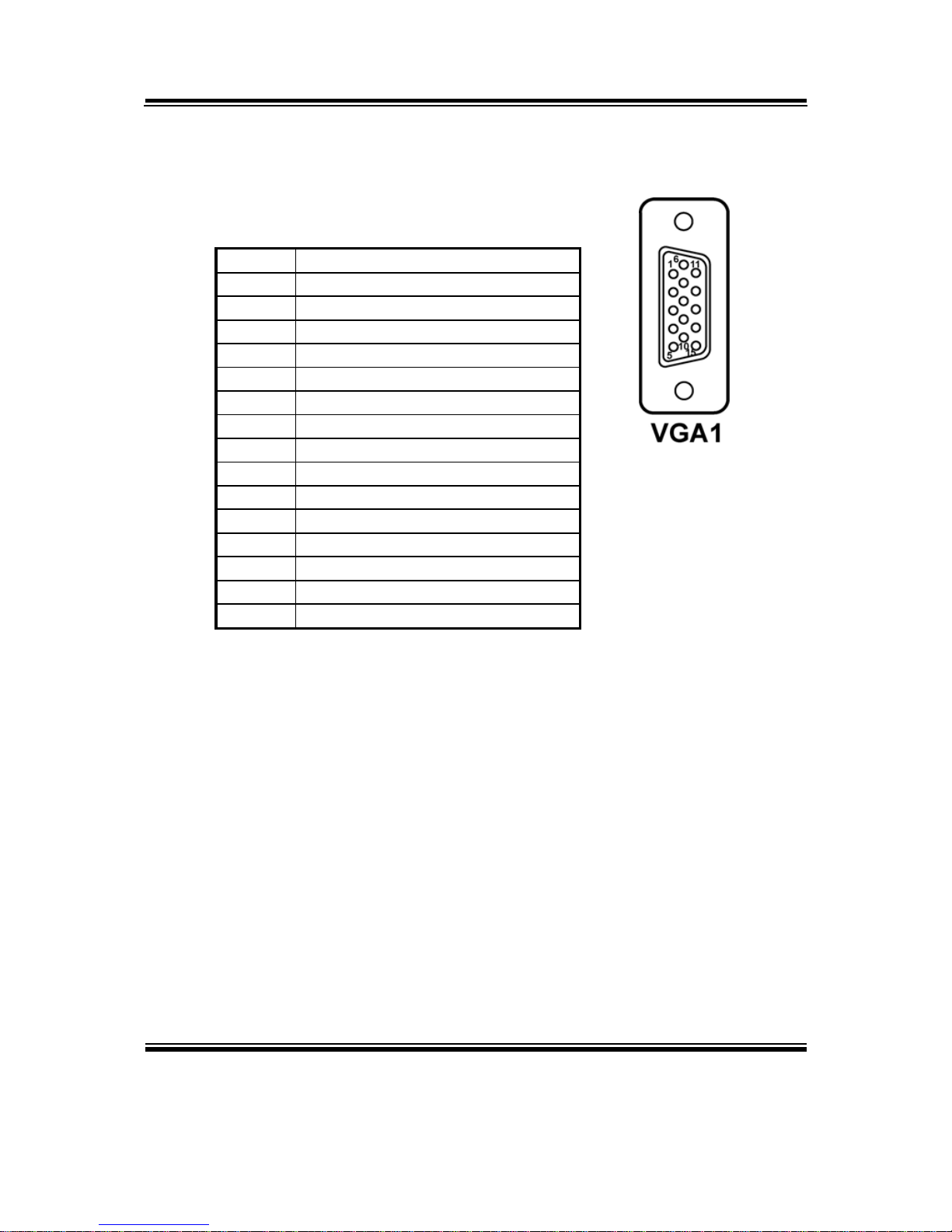
2-18. VGA CONNECTOR
VGA1 : VGA CRT Connector
The pin assignments are as follows:
PIN ASSIGNMENT
1 RED
2 GREEN
3 BLUE
4 NC
5 GND
6 GND
7 GND
8 GND
9 VCC
10 GND
11 NC
12 VGA IIC DATA
13 HSYNC
14 VSYNC
15 VGA IIC CLK
Chapter 2 Hardware Configuration
Page: 2-14
IND-PM855F USER
′
S MANUAL
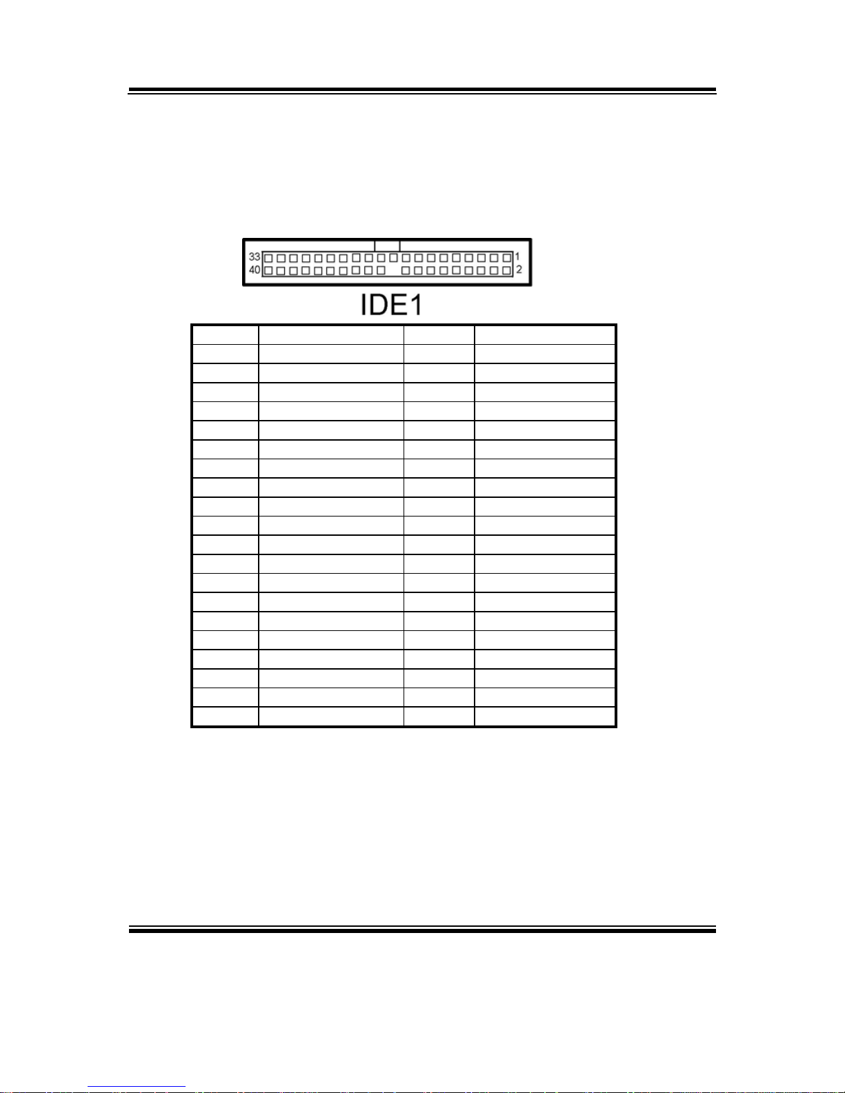
2-19. HARD DISK DRIVE CONNECTOR
IDE1: Hard Disk Drive Connector
The IND-PM855F possesses two HDD connectors, IDE1 and IDE2. The
pin assignments are as follows:
PIN ASSIGNMENT PIN ASSIGNMENT
1 PIDERSTJ 2 GND
3 PDD7 4 PDD8
5 PDD6 6 PDD9
7 PDD5 8 PDD10
9 PDD4 10 PDD11
11 PDD3 12 PDD12
13 PDD2 14 PDD13
15 PDD1 16 PDD14
17 PDD0 18 PDD15
19 GND 20 NC
21 PDREQ 22 GND
23 PDIOWJ 24 GND
25 PDIORJ 26 GND
27 PDIORDY 28 PULL-LOW
29 PDDACKJ 30 GND
31 IRQ14 32 NC
33 PDA1 34 PD66_DECT
35 PDA0 36 PDA2
37 PDCSJ1 38 PDCSJ3
39 IDEACTPJ 40 GND

Chapter 2 Hardware Configuration
IND-PM855F USER′S MANUAL
Page: 2-15
IDE2: Hard Disk Drive Connector
The pin assignments are as follows:
PIN ASSIGNMENT PIN ASSIGNMENT
1 SIDERSTJ 2 GND
3 SDD7 4 SDD8
5 SDD6 6 SDD9
7 SDD5 8 SDD10
9 SDD4 10 SDD11
11 SDD3 12 SDD12
13 SDD2 14 SDD13
15 SDD1 16 SDD14
17 SDD0 18 SDD15
19 GND 20 NC
21 SDREQ 22 GND
23 SDIOWJ 24 GND
25 SDIORJ 26 GND
27 SDIORDY 28 PULL-LOW
29 SDDACKJ 30 GND
31 IRQ15 32 NC
33 SDA1 34 SD66_DECT
35 SDA0 36 SDA2
37 SDCSJ1 38 SDCSJ3
39 IDEACTSJ 40 GND
Chapter 2 Hardware Configuration
Page: 2-16
IND-PM855F USER
′
S MANUAL
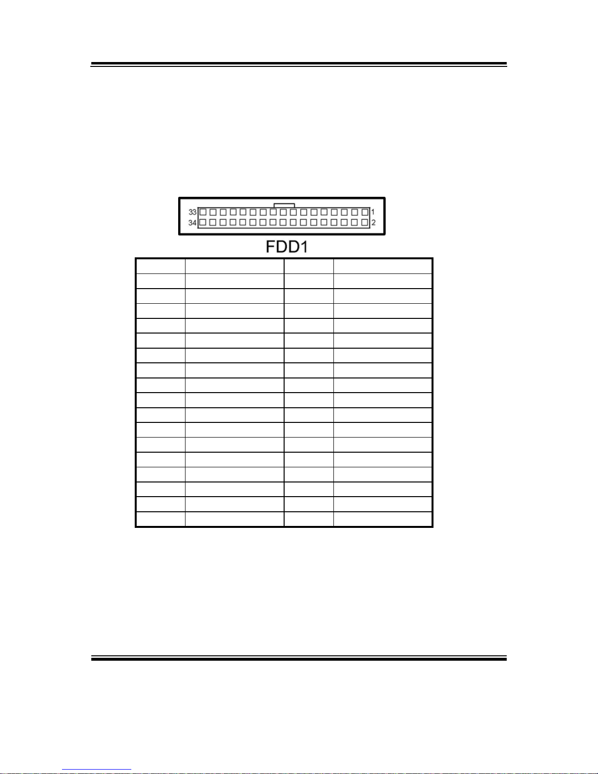
2-20. FLOPPY DISK DRIVE CONNECTOR
FDD1 : Floppy Disk Drive Connector
You can use a 34-pin daisy-chain cable to connect two-FDDs. On one
end of this cable is a 34-pin flat cable to attach the FDD on the board, and
the other side is attaches two FDDs.
The pin assignments are as follows :
PIN ASSIGNMENT PIN ASSIGNMENT
1 GND 2 RWCJ
3 GND 4 NC
5 NC 6 DS1J
7 GND 8 INDEXJ
9 GND 10 MOAJ
11 GND 12 DSBJ
13 GND 14 DSAJ
15 GND 16 MOBJ
17 GND 18 DIRJ
19 GND 20 STEPJ
21 GND 22 WDJ
23 GND 24 WENJ
25 GND 26 TRAK0J
27 GND 28 WPJ
29 GND 30 RDATAJ
31 GND 32 HEADJ
33 GND 34 DSKCHGJ
Chapter 2 Hardware Configuration
IND-PM855F USER′S MANUAL
Page: 2-17
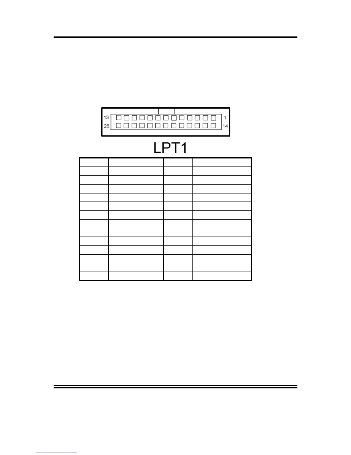
2-21. PRINTER CONNECTOR
LPT1 : Printer Connector
As to link the Printer to the card, you need a cable to connect both DB25
connector and parallel port.
The pin assignments are as follows :
PIN ASSIGNMENT PIN ASSIGNMENT
1 STBJ 14 ALFJ
2 PDR0 15 ERRORJ
3 PDR1 16 PARINITJ
4 PDR2 17 SLCTINJ
5 PDR3 18 GND
6 PDR4 19 GND
7 PDR5 20 GND
8 PDR6 21 GND
9 PDR7 22 GND
10 ACKJ 23 GND
11 BUSY 24 GND
12 PE 25 GND
13 SLCTJ 26 NC
 Loading...