Impala Linear Corporation ILC7080AIM5-50, ILC7080AIM5-36, ILC7080AIM5-33, ILC7080AIM5-30, ILC7080AIM5-285 Datasheet
...
ILC7080/81
50/100mA SOT-23 CMOS RF LDO™ Regulators
Impala Linear Cor poration
Impala Linear Corporation
1
(408) 574-3939
www.impalalinear.com
Sept. 1998
ILC7080/81 1.1
The ILC7080/81 are 50 or 100mA low dropout (LDO) voltage regulators designed to provide a high performance
solution to low power systems.
The devices offer a typical combination of low dropout
and low quiescent current expected of CMOS parts,
while uniquely providing the low noise and high ripple
rejection characteristics usually only associated with
bipolar LDO regulators.
The devices have been optimized to meet the needs of
modern wireless communications design; Low noise, low
dropout, small size, high peak current, high noise immunity. The ILC7080/81 are designed to make use of low cost
ceramic capacitors while outperforming other devices that
require tantalum capacitors.
General Description
Features
• Ultra low 1mV dropout per 1mA load
• 1% output voltage accuracy
• Uses low ESR ceramic output capacitor to minimize
noise and output ripple
• Only 100µA ground current at 100mA load
• Ripple rejection up to 85dB at 1kHz, 60dB at 1MHz
• Less than 80µV
RMS
noise at BW = 100Hz to 100kHz
• Excellent line and load transient response
• Over current / over temperature protection
• Guaranteed up to 80/150mA output current
• Industry standard five lead SOT-23 package
• Fixed 2.85V, 3.0V, 3.3V, 3.6V, 4.7V, 5.0V and adjustable
output voltage options
• Metal mask option available for custom voltages between
2.5 to 10V
• Cellular phones
• Wireless communicators
• PDAs / palmtops / organizers
• Battery powered portable electronics
Applications
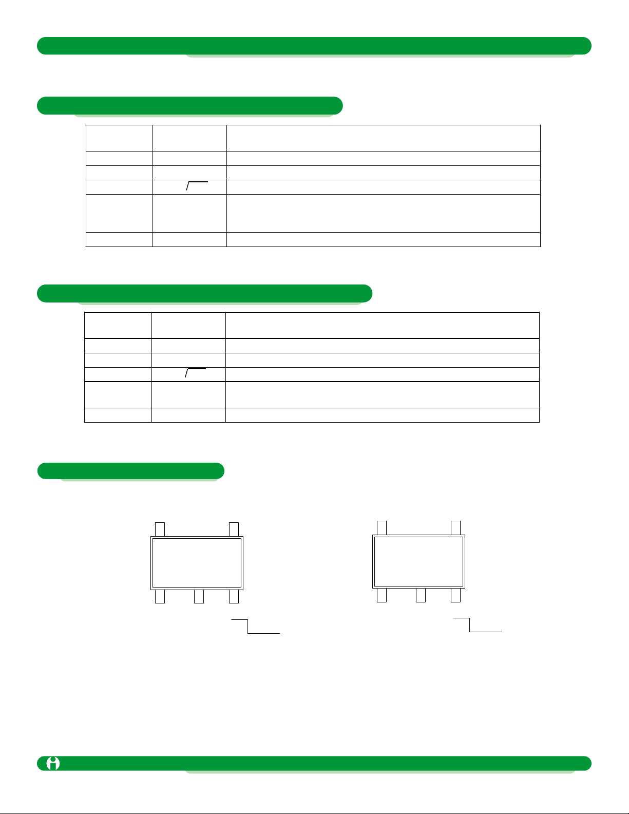
Typical Circuit
ILC7080
ILC7081
V
OUT
V
IN
C
OUT
C
NOISE
SOT23-5
123
45
ON
OFF
Ordering Information (TA = -40°C to +85°C)
ILC7080AIM5-xx
50mA, fixed voltage
ILC7080AIM5-ADJ
50mA adjustable voltage
ILC7081AIM5-xx
100mA, fixed voltage
ILC7081AIM5-ADJ
100mA, adjustable voltage
Note: Fixed voltage options are defined by 2-digit code as shown in the
package markings information section of the datasheet.
50/100mA SOT-23 CMOS RF LDO™ Regulators
Impala Linear Corporation
2
(408) 574-3939
www.impalalinear.com
Sept. 1998
ILC7080/81 1.1
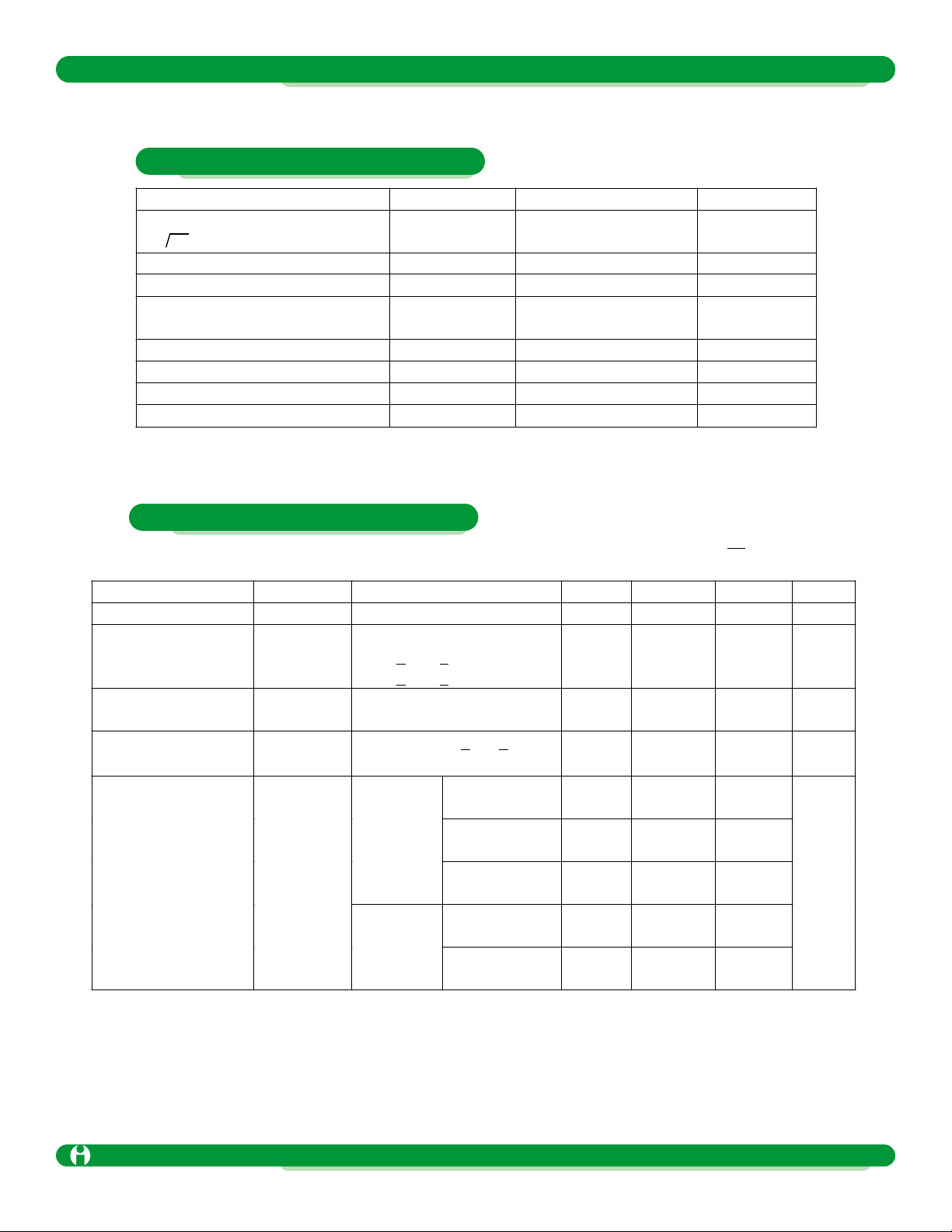
Pin Description ILC7081/81-xx (fixed voltage version)
Pin
Number
Pin Name
Pin Description
1
VIN
Connect direct to supply
2
GND
Ground pin. Local ground for C
NOISE
and C
OUT
.
3
ON/OFF
By applying less than 0.4V to this pin the device will be turned off.
4
C
NOISE
Optional noise bypass capacitor may be connected between this
pin and GND (pin 2). Do not connect C
NOISE
directly to the main
power ground plane.
5
V
OUT
Output Voltage. Connect C
OUT
between this pin and GND (pin 2)
Pin Description ILC7081/81-ADJ (adjustable voltage version)
Pin
Number
Pin Name
Pin Description
1
VIN
Connect direct to supply
2
GND
Ground pin. Local ground for C
NOISE
and C
OUT
.
3
ON/OFF
By applying less than 0.4V to this pin the device will be turned off.
4
V
ADJ
Voltage feedback pin to set the adjustable output voltage. Do not
connect a capacitor to this pin.
5
V
OUT
Output Voltage. Connect C
OUT
between this pin and GND (pin 2)
Pin Package Configurations
ILC7080-xx
ILC7081-xx
SOT23-5
ON
OFF
C
NOISE
V
IN
V
OUT
GND
123
45
ILC7080-ADJ
ILC7081-ADJ
SOT23-5
ON
OFF
V
ADJ
V
IN
V
OUT
GND
123
45
50/100mA SOT-23 CMOS RF LDO™ Regulators
Impala Linear Corporation
3
(408) 574-3939
www.impalalinear.com
Sept. 1998
ILC7080/81 1.1
Parameter
Symbol
Ratings
Units
Input voltage
On/Off Input voltage
VIN
V
ON/OFF
-0.3 to +13.5
-0.3 to V
IN
V
Output Current
I
OUT
Short circuit protected
mA
Output voltage
V
OUT
-0.3 to VIN+0.3
V
Package Power Dissipation
(SOT-23-5)
PD
250
(Internally Limited)
mW
Maximum Junction Temp Range
T
J(max)
-40~+150
°C
Storage Temperature
T
STG
-40~+125
°C
Operating Ambient Temperature
TA
-40 to +85
°C
Package Thermal Resistance
θJA
333
°C/W
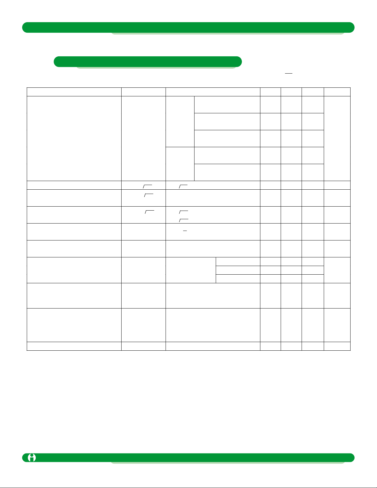
Absolute Maximum Ratings (Note 1)
Absolute Maximum Ratings (Note 1)
Parameter
Symbol
Conditions
Min
Typ
Max
Units
Input Voltage Range
VIN
2
13
V
Output voltage
V
OUT
I
OUT
= 1mA
1mA < I
OUT
< 100mA
1mA < I
OUT
< 100mA
-1
-1.5
-3.5
V
OUT(NOM)
+1
1.5
+3.5
%
Feedback Voltage
(ADJ version)
V
ADJ
1.215
1.202
1.240
1.265
1.278
V
Line Regulation
∆V
OUT
/
(V
OUT
*∆VIN)
V
OUT(NOM)
+ 1V < VIN < 12V
0.007
0.014
0.032
%/V
I
OUT
= 0mA
0.1
1
2
I
OUT
= 10mA
10
25
35
7080/81
I
OUT
= 50mA
50
75
100
I
OUT
= 100mA
100
150
200
Dropout voltage
(Note 3)
VIN – V
OUT
7081 only
I
OUT
= 150mA
150
225
300
mV
Unless otherwise specified, all limits are at TA= 25°C; VIN= V
OUT(NOM)
+ 1V, I
OUT
= 1mA, C
OUT
= 1µF, V
ON/OFF
= 2V.
Boldface limits apply over the operating temperature range. (Note 2)
50/100mA SOT-23 CMOS RF LDO™ Regulators
Impala Linear Corporation
4
(408) 574-3939
www.impalalinear.com
Sept. 1998
ILC7080/81 1.1
Parameter
Symbol
Conditions
Min
Typ
Max
Units
I
OUT
= 0mA
95
200
220
I
OUT
= 10mA
100
220
240
7080/81
I
OUT
= 50mA
100
220
240
I
OUT
= 100mA
100
240
260
Ground Pin Current
I
GND
7081
only
I
OUT
= 150mA
115
260
280
µA
Shutdown (OFF) Current
I
ON/OFF
V
ON/OFF
= 0V
0.1 2 µA
ON/OFF Input Voltage
V
ON/OFF
High = Regulator On
Low = Regulator Off
2.0 13
0.6
V
ON/OFF Pin Input Current
(Note 5)
I
IN(ON/OFF)
V
ON/OFF
= 0.6V, regulator OFF
V
ON/OFF
= 2V, regulator ON
0.3 1
µA
Peak Output Current
(Note 4)
I
OUT(PEAK)
V
OUT
> 0.95V
OUT(NOM)
,
tpw = 2ms
400
500 mA
Output Noise Voltage
eN
BW = 300Hz to 50kHz,
C
NOISE
= 0.01µF
80 µV
RMS
freq = 1kHz
85
freq = 10kHz
70
Ripple Rejection
∆V
OUT
/∆VIN
C
OUT
= 4.7µF,
I
OUT
= 100mA
freq = 1MHz
60
dB
Dynamic Line Regulation
∆V
OUT(line)
VIN: V
OUT(NOM)
+ 1V to
V
OUT(NOM)
+ 2V,
tr/tf = 2µs; I
OUT
= 100mA
4
mV
Dynamic Load Regulation
∆V
OUT(load)
I
OUT
: 0 to 100mA;
d(I
OUT
)/dt = 100mA/µs
with C
OUT
= 0.47µF
with C
OUT
= 2.2µF
50
25
mV
Short Circuit Current
ISC
V
OUT
= 0V
600 mA
Note 1: Absolute maximum ratings indicate limits which when exceeded may result in damage to the component. Electrical specifications do not apply when operating the
device outside of its rated operating conditions.
Note 2: Specified Min/Max limits are production tested or guaranteed through correlation based on statistical control methods. Measurements are taken at constant junction
temperature as close to ambient as possible using low duty pulse testing.
Note 3: Dropout voltage is defined as the input to output differential voltage at which the output voltage drops 2% below the nominal value measured with a 1V differential.
Note 4: Guaranteed by design
Note 5: The device’s shutdown pin includes a 2MW internal pull down resistor connected to ground.
Electrical Characteristics ILC7080/81AIM5 (cont.)
Unless otherwise specified, all limits are TA= 25°C; VIN= V
OUT(NOM)
+ 1V, I
OUT
= 1mA, C
OUT
= 1µF, V
ON/OFF
= 2V.
Boldface limits apply over the operating temperature range. (Note 2)

50/100mA SOT-23 CMOS RF LDO™ Regulators
Impala Linear Corporation
5
(408) 574-3939
www.impalalinear.com
Sept. 1998
ILC7080/81 1.1
The ILC7080/81 LDO design is based on an advanced circuit configuration for which patent protection has been
applied. Typically it is very difficult to drive a capacitive output with an amplifier. The output capacitance produces a
pole in the feedback path, which upsets the carefully tailored dominant pole of the internal amplifier. Traditionally
the pole of the output capacitor has been “eliminated” by
reducing the output impedance of the regulator such that
the pole of the output capacitor is moved well beyond the
gain bandwidth product of the regulator. In practice, this is
difficult to do and still maintain high frequency operation.
Typically the output impedance of the regulator is not simply resistive, such that the reactive output impedance interacts with the reactive impedance of the load resistance and
capacitance. In addition, it is necessary to place the dominant pole of the circuit at a sufficiently low frequency such
that the gain of the regulator has fallen below unity before
any of the complex interactions between the output and the
load occur. The ILC7080/81 does not try to eliminate the
output pole, but incorporates it into the stability scheme.
The load and output capacitor forms a pole, which rolls off
the gain of the regulator below unity. In order to do this the
output impedance of the regulator must be high, looking like
a current source. The output stage of the regulator
becomes a transconductance amplifier, which converts a
voltage to a current with a substantial output impedance.
The circuit which drives the transconductance amplifier is
the error amplifier, which compares the regulator output to
the band gap reference and produces an error voltage as
the input to the transconductance amplifier. The error amplifier has a dominant pole at low frequency and a “zero”
which cancels out the effects of the pole. The zero allows
the regulator to have gain out to the frequency where the
output pole continues to reduce the gain to unity. The configuration of the poles and zero are shown in figure 1.
Instead of powering the critical circuits from the unregulated input voltage, the CMOS RF LDO powers the internal
circuits such as the bandgap, the error amplifier and most
of the transconductance amplifier from the boot strapped
regulated output voltage of the regulator. This technique
offers extremely high ripple rejection and excellent line transient response.
A block diagram of the regulator circuit used in the
ILC7080/81 is shown in figure 2, which shows the input-tooutput isolation and the cascaded sequence of amplifiers
that implement the pole-zero scheme outlined above.
The ILC7080/81 were designed in a CMOS process with
some minor additions, which allow the circuit to be used at
input voltages up to 13V. The resulting circuit exceeds the
frequency response of traditional bipolar circuits. The
ILC7080/81 is very tolerant of output load conditions with
the inclusion of both short circuit and thermal overload protection. The device has a very low dropout voltage, typically a linear response of 1mV per milliamp of load current,
and none of the quasi-saturation characteristics of a bipolar
output device. All the good features of the frequency
response and regulation are valid right to the point where
the regulator goes out of regulation in a 4mV transition
region. Because there is no base drive, the regulator is
capable of providing high current surges while remaining in
regulation. This is shown in the high peak current of 500mA
which allows for the ILC7080/81 to be used in systems that
require short burst mode operation.
DOMINANT POLE
OUTPUT POLE
85 dB
COMPENSATING
ZERO
UNITY GAIN
FREQUENCY
GAIN
Figure 1: ILC7080/81 RF LDO frequency response
Operation
 Loading...