Impala Linear Corporation ILC707M, ILC706N, ILC705N, ILC705M, ILC708M Datasheet
...
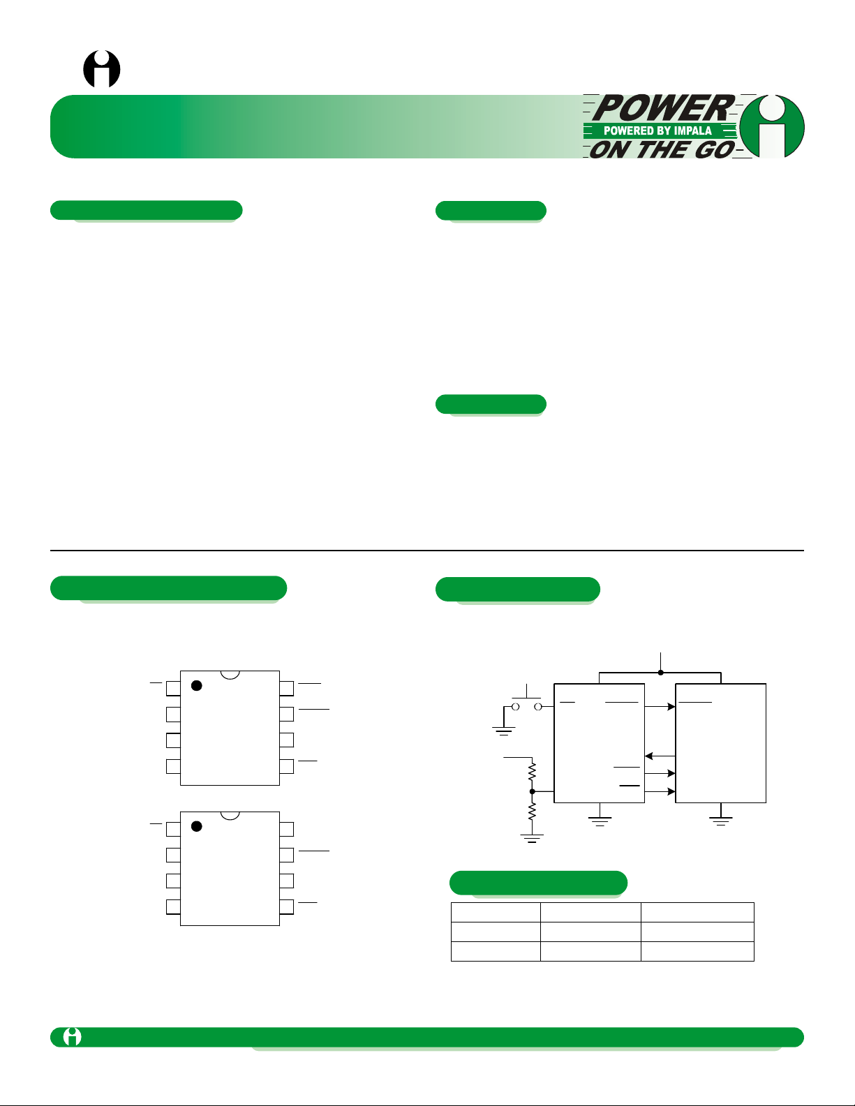
The ILC705/ILC706/ILC707/ILC708 are low cost microprocessor supervisory circuits that monitor power supplies in microprocessor based systems. Circuit functions
include a watchdog timer, microprocessor reset, power
failure warning and a debounced manual reset input.
The ILC705 and ILC706 offer a watchdog timer function
while the ILC707 and ILC708 have an active high reset
output in addition to the active low reset output.
Supply voltage monitor levels of 4.65V and 4.4V are
available. The ILC705/ILC707 have a nominal reset
threshold level of 4.65V while the ILC706 and ILC708
have a 4.4V nominal reset threshold level. When the supply voltage drops below the respective reset threshold
level, RESET is asserted.
ILC705/706/707/708
mP Supervisory Circuit
Impala Linear Cor poration
Impala Linear Corporation
1
(408) 574-3939
www.impalalinear.com
Sept 1999
ILC705-708 1.0
! 4.4V or 4.65V Precision Voltage Monitor
! 200ms Reset Pulse Width
! Debounced TTL/CMOS Compatible Manual Reset Input
! Watchdog Timer with 1.6 sec Timeout (ILC705/ILC706)
! Voltage Monitor for Early Power Fail Warning or Low
Battery Detect
! 8-Pin SOIC or DIP Package
! Computers
! Controllers
! Critical Microprocessor Power Monitoring
! Intelligent Instruments
! Portable Equipment
! Controllers
ILC705
ILC706
ILC707
ILC708
Top View
MR
PFO
VCC
2
1 8
6 WDI
PFI
RESET
GND
4
3
5
7
N Package - 8 Lead Plastic DIP Package
M Package - 8 Lead Plastic SOIC Package
2
1 8
6
4
3
5
7
WDO
MR
PFO
VCC
NC
PFI
RESET
GND
RESET
Part Package Temp. Range
ILC70_N 8-Lead PDIP -40°C to +85°C
ILC70_M 8-Lead SOIC -40°C to +85°C
ILC705
ILC706
µµ
P
VCC
+5 V (Regulated)
VCC
WDI
NMI
WDO
GNDPFI
I/O Line
MR
RESET RESET
Manual
Reset
DC Voltage
(Unregulated)
InterruptPFO
Typical Circuit
Pin Package Configuration
General Description
Features
Applications
Ordering Information

mP Supervisory Circuit
Impala Linear Corporation
2
(408) 574-3939
www.impalalinear.com
Sept 1999
ILC705-708 1.0
Parameter Symbol Ratings Units
V
CC
-0.3 to 6.0 VTerminal Volta ge
All other inputs
-0.3 to (VCC + 0.3)
V
Input Current V
CC,
GND 25 mA
Output Current All outputs 20 mA
Operating Temperature Range T
A
-40 to +85 °C
Storage Temperature Range -65 to +150 °C
Lead Temperature (Soldering, 10 sec.) 300 °C
PDIP 475 mWPower Dissipation
SOIC 400 mW
Stresses above those listed under ABSOLUTE MAXIMUM RATINGS may cause permanent device failure. Functionality
at or above these limits is not implied. Exposure to absolute maximum ratings for extended periods may affect device
reliability. Operating ranges define those limits between which the functionality of the device is guaranteed.
VCC = 4.75 V to 5.5 V for ILC705/I LC707, VCC = 4.5 V to 5.5 V for ILC706/I LC708, TA = Operating Temperature Range, unless
otherwise noted.
Parameter
Conditions
Min
Typ
Max
Units
Operating Voltage Range, VCC
ILC70__
1.4 5.5
V
Supply Current, ICC
ILC70__
60
µA
Reset Voltage Threshold
ILC705, ILC707
ILC706, ILC708
4.5
4.25
4.65
4.4
4.75
4.5
V
Reset Threshold Hysteresis
40 mV
Reset Pulse Width, tRS
140
200
280
ms
RESET Output Voltage
I
SOURCE
= 800 µA
I
SINK
= 3.2 mA
I
SINK
= 50 µA, VCC = 1.4V
VCC – 1.5V
0.4
0.3
V
RESET Output Voltage
I
SOURCE
= 800 µA
I
SINK
= 1.2 mA
VCC – 1.5V
0.4
V
Watchdog Timeout Period, tWD
1.0
1.6
2.25
sec
WDI Minimum Input Pulse, tWP
VIL = 0.4V, VIH = 80% of VCC
50
ns
WDI Threshold Voltage
VIH, VCC = 5V
VIL, VCC = 5V
3.5
0.8
V
WDI Input Current
WDI = 0V
WDI = VCC
-150
-50
50 150
µA
WDO Output Voltage
I
SOURCE
800 µA
I
SINK
= 1.2 mA
VCC – 1.5V
0.4
V
MR Pull-Up Current
MR = 0V
100
250
600
µA
MR Pulse Width, tMR
150
ns
MR Input Threshold
VIL
VIH 2.0
0.8
V
MR to Reset Output Delay, tMD
250
ns
PFI Input Threshold
VCC = 5V
1.2
1.25
1.3
V
PFI Input Current
-25
0.01
25
nA
PFO Output Voltage
I
SINK
= 3.2mA
VCC = 5V, I
SOURCE
= 800 µA
VCC - 1.5V
0.4
V
Absolute Maximum Ratings
Electrical Characterisitcs
 Loading...