Impala Linear Corporation ILC6370BP-50, ILC6370BP-33, ILC6370BP-25, ILC6370AP-50, ILC6371CP-50 Datasheet
...
ILC 6370/71
SOT-89 Step up Switching Regulator with Shutdown
Impala Linear Cor poration
Impala Linear Corporation
1
(408) 574-3939
www.impalalinear.com
July 1999
ILC6370/1 1.3
50mA boost converter in 5-lead SOT-89 package. Only 3
external components are needed to complete the switcher
design, and frequency options of 50, 100, and 180kHz gives
the designer the ability to trade off system needs with
switcher design size.
87% max duty cycle gives conversion efficiencies of 85%.
Standard voltage options of 2.5V, 3.3V, and 5.0V at ±2.5%
accuracy feature on-chip phase compensation and softstart design.
ILC6371 drives an external transistor for higher current
switcher design, with all of the features and benefits of
the ILC6370.
! 85% efficiency at 50mA
! Start-up voltages as low as 900mV
! ±2.5% accurate outputs
! Complete switcher design with only 3 external components
! 50, 100 and 180kHz switching frequency versions available
! Shutdown to 0.5µA
! External transistor option allows several hundred milliamp
switcher design
! Cellular Phones, Pagers
! Portable Cameras and Video Recorders
! Palmtops and PDAs
Ordering Information*
ILC6370CP-25
2.5V±2.5%@50kHz
ILC6370CP-25
3.3V±2.5%@50kHz
ILC6370CP-50
5.0V±2.5%@50kHz
ILC6370BP-25
2.5V±2.5%@100kHz
ILC6370BP-33
3.3V±2.5%@100kHz
ILC6370BP-50
5.0V±2.5%@100kHz
ILC6370AP-25
2.5V±2.5%@180kHz
ILC6370AP-33
3.3V±2.5%@180kHz
ILC6370AP-50
5.0V±2.5%@180kHz
ILC6371CP-25
2.5V±2.5%@50k Hz, ex ternal xtor
ILC6371CP-33
3.3V±2.5%@50k Hz, ex ternal xtor
ILC6371CP-50
5.0V±2.5%@50k Hz, ex ternal xtor
ILC6371BP-25
2.5V±2.5%@100k Hz , ex ternal xtor
ILC6371BP-33
3.3V±2.5%@100k Hz , ex ternal xtor
ILC6371BP-50
5.0V±2.5%@100k Hz , ex ternal xtor
ILC6371AP-25
2.5V±2.5%@180k Hz , ex ternal xtor
ILC6371AP-33
3.3V±2.5%@180k Hz , ex ternal xtor
ILC6371AP-50
5.0V±2.5%@180k Hz , ex ternal xtor
Standard Product offering comes in tape and reel,
quantity 1000 per reel, orientation right for SOT-89
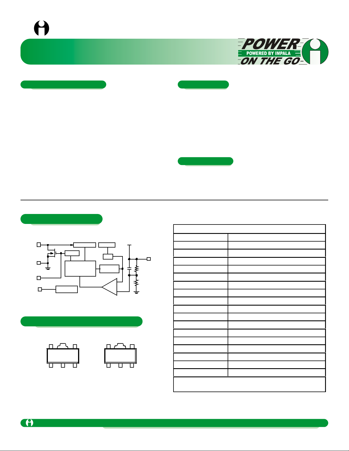
VLX LIMITER
PWM Controlled
BUFFER
L
X
V
SS
EXT
+
-
CHIP ENABLE
OSC
50/100/180KHz
V
DD
V
OUT
CE
Phase comp
V
re f
Slow St art
VDD is internally connected to the V
OUT
pin.
SOT -89-5
(TOP VIEW)
132
V
OUT
CE
L
X
45
V
SS
N/C
SOT -89-5
(TOP VI EW )
132
V
OUT
CE
EXT
45
V
SS
N/C
ILC6370 ILC6371
General Description
Features
Applications
Block Diagram
Pin-Package Configurations

SOT-89 Step up Switching Regulator with Shutdown
Impala Linear Corporation
2
(408) 574-3939
www.impalalinear.com
July 1999
ILC6370/1 1.3
Parameter
Symbol
Ratings
Units
V
OUT
Input Voltage Pin
V
OUT
12
V
CE Input Voltage
VCE
12
V
Voltage on pin LX
VLX
12
V
Current on pin LX
ILX
400
mA
Voltage on pin EXT
V
EXT
0.3 ~V
OUT
+0.3
V
Current pin EXT
I
EXT
+50
mA
Continuous Total Power Dissipation
(SOT-89-5)
PD
500
mW
Operating Ambient Temperature
T
OPR
-30~+80
οC
Storage Temperature
T
STG
-40~+125
οC
Parameter
Symbol
Conditions
Min
Typ
Max
Units
Output Voltage
V
OUT
3.218
3.300
3.383
V
Input Voltage
VIN 10
V
Oscillation Startup Voltage
V
ST2
LX :10kΩ Pull-up to.5V, V
OUT
= VST
500
600 mA
Operation Startup Voltage
V
ST1
I
OUT
+1mA
55
86
µA
Supply Current 1
IDD1
LX :10kΩ Pull-up to.5V, V
OUT
= 4.5V
1.5
2.5
µA
Supply Current 1
IDD2
Open Loop Measurement, V
S/D
= VIN,
VLX =V
IN-
0.4V, V
OUT
= 3V
0.64
0.85
Ω
L
X
Switch-On Resistance
R
SWON
Open Loop Measurement, V
OUT
= V
IN,
V
LX
= 0V
2.0
µA
L
X
Leakage Current
ILXL
Measure Waveform at EXT pin V
IN
= 3.6V
I
OUT
= 20mA
255
300
345
KHz
Oscillator Frequency
F
OSC
100 %
Maximum Duty Ratio
MAXDTY
No Load
10
17
25
%
Satndb-by Current
I
STB
95 %
CE "High " Voltage
V
CEH
Minimum V
IN
When V
ref
does not start up
1 1.8
V
CE "Low " Voltage
V
CEL
V
ref
rises to 0V from 0.9V
6.0
10.0
16.0
msec
Note: Unless otherwise spcified, VIN= V
OUT
x 0.6, I
OUT
= 50mA. See Schematic, figure 1.
Absolute Maximum Ratings (TA = 25°C)
V
OUT
= 5.0V, F
OSC
= 100kHz, TA= 25°C, Test Circuit of figure 1
Elcetrical Characteristics ILC6370BP-50

SOT-89 Step up Switching Regulator with Shutdown
Impala Linear Corporation
3
(408) 574-3939
www.impalalinear.com
July 1999
ILC6370/1 1.3
Parameter
Symbol
Conditions
Min
Typ
Max
Units
CE “High” Current
I
CEH
LX: 10kΩ pull-up to 5V, V
CE
= V
OUT
= 4.5V
0.25
µA
CE “Low” Current
I
CEL
LX: 10kΩ pull-up to 5V, V
OUT
=
4.5V, VCE = 0V
-0.25
µ
LX Limit Voltage
V
LXLMT
LX: 10kΩ pull-up to 5V, V
OUT
= 4.5V, F
OSC
> F
OSC
x 2
(1)
0.7 1.1
V
Efficie ncy
EFFI
85 %
Parameter
Symbol
Conditions
Min
Typ
Max
Units
Output Voltage
V
OUT
4.875 5.000
5.125
V
Input Voltage
V
IN
10
V
Oscillation Startup Voltage
V
ST
EXT: 10kΩ pull-up to 5V, V
OUT
= V
ST
0.8
V
Supply Current 1
IDD 1
EXT: 10kΩ pull-up to 5V, V
OUT
= 4.5V
38.4
64.1
µA
Supply Current 2
IDD 2
EXT: 10kΩ pull-up to 5V, V
OUT
= 5.5V
6.9
13.8
µA
EXT “High” On-Resistance
R
EXTH
EXT: 10kΩ pull-up to 5V, V
OUT
= 4.5V,
V
EXT
= 4.1V
30
50
Ω
EXT “Low” On-Resistance
R
EXTL
V
EXT
= 0.4V, V
OUT
= 5.5V
30
50
Ω
Oscillator Frequency
F
OSC
EXT: 10kΩ pull-up to 5V, V
OUT
= 4.5V,
Measuring of EXT pin
85
100
115
kHz
Maximum Duty Ratio
MAXDTY
EXT: 10kΩ pull-up to 5V, V
OUT
= 4.5V,
Measuring of EXT pin
80
87
92
%
Stand-by Current
I
STB
EXT: 10kΩ pull-up to 5V, V
OUT
= 4.5V
0.5
µA
CE “High” Voltage
V
CEH
EXT: 10kΩ pull-up to 5V, V
OUT
= 4.5V,
Existance of L
X
Oscillation
0.75
V
CE “Low” Voltage
V
CEL
EXT: 10kΩ pull-up to 5V, V
OUT
= 4.5V,
Stopped L
X
Oscillation
0.20
V
CE “High” Current
I
CEH
EXT: 10kΩ pull-up to 5V, V
OUT
= VCE = 4.5V
0.25
µA
CE “Low” Current
I
CEL
EXT: 10kΩ pull-up to 5V, V
OUT
= 4.5V, VCE = 0V
-0.25
µA
Efficiency
EFFI
85 %
Slow Start Time
T
SS
10 msec
V
OUT
= 5.0V, F
OSC
= 100kHz, TA= 25°C; Test Circuit of figure 1
1. Switching frequency determined by delay time of internal comparator to turn LX“OFF,” and minimum “ON” time as
determined by MAXDTY spec.
V
OUT
= 5.0V, F
OSC
= 100kHz, TA= 25°C; Test Curcuit of figure 2.
Electrical Characteristics ILC6370BP-50
Electrical Characteristics ILC6371BP-50
 Loading...