ILC6360
Step-Up/Step Down DC-DC Converter for
1-Cell Lithium-Ion Batteries
Impala Linear Cor poration
Impala Linear Corporation
1
(408) 574-3939
www.impalalinear.com
Jan 1999
ILC6360 1.1
The ILC6360 step-up/step-down DC-DC converter is a
switch mode converter, capable of supplying up to 500mA
output current, at a fixed or user selectable output voltage.
The range of input, and output voltage options makes the
ILC6360 ideal for Lithium-ion (Li-ion) , or any other battery
application, where the input voltage range spans above and
below the regulated output voltage. When ILC6360’s input
voltage exceeds the output voltage by more than 800mV,
the output will begin to track the input linearly.
Configured as a 300kHz, fixed frequency PWM boost converter, the ILC6360 performs the buck operation by seamlessly switching to PFM, when the output voltage rises near
the positive range of regulation. However, since the transition
point between PWM and PFM mode is dependent upon both
line, and load regulation, under certain conditions, regulation
will remain in PWM mode even in the buck mode of operation.
The ILC6360 is unconditionally stable with no external compensation; the sizes of the input and output capacitors influence the ripple on the input, and output voltages. Since the
ILC6360 has an internal synchronous rectifier, the standard
fixed voltage version requires minimal external components:
an inductor, an input capacitor, and an output capacitor. An
additional 10µF ceramic output capacitor will help reduce
output ripple voltage.
Other features include an external sync input for synchronizing the PWM frequency, low battery input detector with
100ms transient rejection delay built-in, and, a power good
indicator useful as a system power on reset.
• ILC6360CIR-36: Fixed 3.6V output; custom
voltages possible
• ILC6360CIR-ADJ: Adjustable output to 6V maximum
• Capable of 500mA output current
• Peak efficiency: > 90% at V
OUT
= .6V,I
OUT
= 300mA,
V
IN =
3.6V
• No external diode is required (synchronous rectification)
• Battery input current of 250mA at no load
• True load disconnect from battery input in shutdown (1mA)
• OSC freq: 300kHz ±15%
• External freq synchronization from 150kHz to 500kHz
• Low battery detector with 100ms transient rejection delay
• Power good output flag when V
OUT
is in regulation
• MSOP-8 package
• Cellular phones
• Palmtops, PDAs and portable electronics
• Equipment using single Lithium-Ion batteries
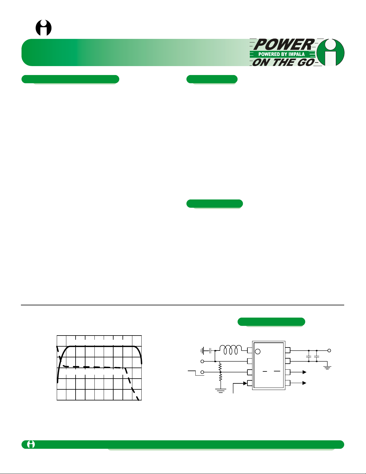
Optimized to Maximize Battery Life
90
80
70
Time
4.2
3.6
3.0
Battery Voltage (V)
ILC6360 Efficiency (%)
15µH
Ext Sync
(Connect to GND if unused)
L
C
OUT
ILC6360CIR-ADJ
L
X
V
IN
LBI/SD
SYNC
GND
LBO
V
FB
V
OUT
V
OUT
1
2
3
4
8
7
6
5
+
V
IN
+
100µF
C
IN
+
10µF 100µF
3.6V/500mA
Low Battery
Detector Output
Power Good Output
2.7V to 4.2V
R5
R6
MSOP-8
ON
OFF
ILC6360 Efficiency @ I
OUT
= 300mA
Typical Li-ion Battery Discharge Curve
Typical Step-up/Step-down Application Circuit
(Note: R5 and R6 are required only if LBI feature is used)
Typical Performance Characteristics for 1-cell Li-ion
General Description
Features
Applications
Patent Pending

Step-Up/Step-Down DC-DC Converter for 1-Cell Lithium-Ion Batteries
Impala Linear Corporation
2
(408) 574-3939
www.impalalinear.com
Jan 1999
ILC6360 1.1
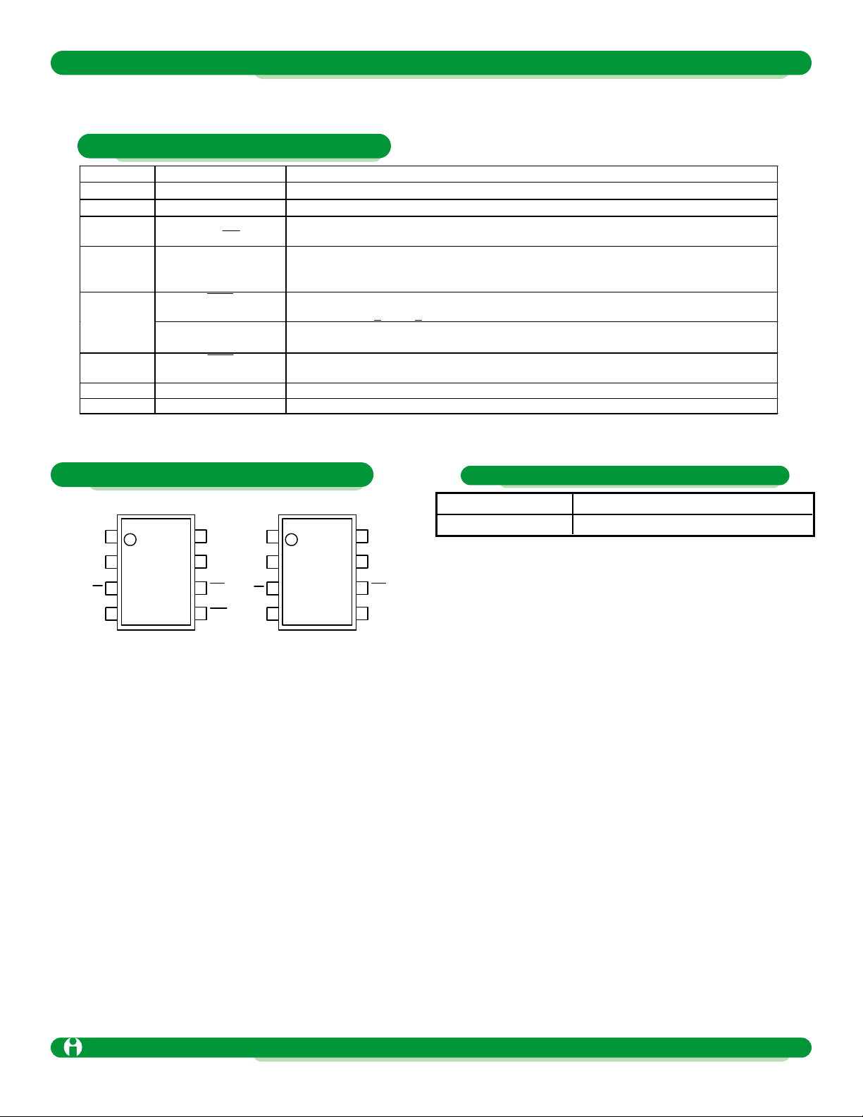
Pin Number
Pin Name
Pin Description
1
L
x
Inductor input. Inductor L connected between this pin and the battery
2
V
IN
Connect directly to battery
3
LBI/SD
Low battery detect input and shutdown. Low battery detect threshold is set with this pin
using a potential divider. If this pin is pulled to logic low then the device will shutdown.
4
SYNC
A logic level signal referenced to VIN, at a frequency between 150kHz and 500kHz on
this pin will over-ride the internal 300kHz oscillator. If the SYNC function is unused, pin
4 should be connected to ground
5
POK
(ILC6382CIR-XX)
This open drain output pin will go high when output voltage is within regulation,
0.92*V
OUT (NOM)
< V
OUT
< 0.98*V
OUT (NOM)
V
FB
(ILC6382CIR-ADJ)
This pin sets the adjustable output voltage via an external resistor divider network. The
formula for choosing the resistors is shown in the “Applications Information“ section.
6
LBO
This open drain output will go low if the battery voltage is below the low battery
threshold set at pin 3
7
GND
Connect this pin to the battery and system ground
8
V
OUT
This is the regulated output voltage
L
X
V
IN
LBI/SD
SYNC
GND
LBO
V
FB
V
OUT
1
2
3
4
8
7
6
5
MSOP-8
(TOP VIEW)
L
X
V
IN
LBI/SD
SYNC
GND
LBO
POK
V
OUT
1
2
3
4
8
7
6
5
MSOP-8
(TOP VIEW)
ILC6360CIR-36
ILC6360CIR-ADJ
ILC6360CIR-36
ILC6360CIR-ADJ
3.6V output, MSOP-8 package
Adjustable output, MSOP-8 package
Pin Functions ILC6360CIR-36
PIN-PACKAGE CONFIGURATIONS
Ordering Information (TA= -40°C to +85°C)

Step-Up/Step-Down DC-DC Converter for 1-Cell Lithium-Ion Batteries
Impala Linear Corporation
3
(408) 574-3939
www.impalalinear.com
Jan 1999
ILC6360 1.1
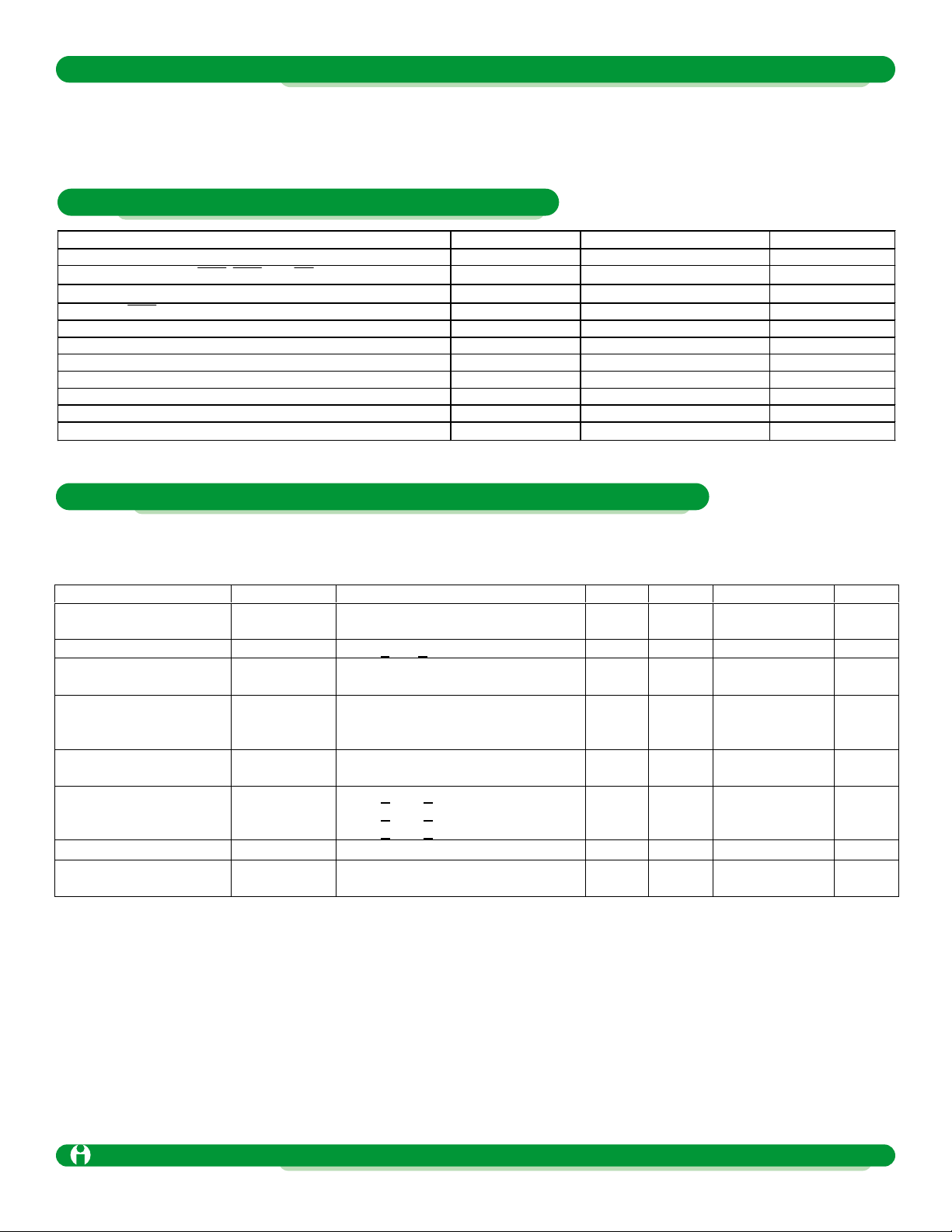
Parameter
Symbol
Ratings
Units
Voltage on V
OUT
pin
V
OUT
-0.3 to 7
V
Voltage on LBI, Sync, LBO, POK, LBI/SD, VFB, LX and VIN pins
-
-0.3 to 7
V
Peak switch current on LX pin
IL
X
1
A
Current on LBO pin
I
sink(LBO)
5
mA
Continuous total power dissipation at 85°C
Pd
400
mW
Short circuit duration
ISC 1 sec
Operating ambient temperature
TA
-40 to 85
°C
Maximum junction temperature
T
J (max)
170
°C
Storage temperature
T
stg
-40 to 125
°C
Lead temperature (soldering 10 sec)
300
°C
Package thermal resistance
θJA
206
°C/W
Parameter
Symbol
Conditions
Min
Typ
Max
Units
Input Voltage
V
IN
V
OUT
= V
OUT(nominal)
± 4%
(Note 3)
2.7
V
OUT (nom)
+0.8
V
Output Voltage
V
OUT
2.8V < VIN < 4.2V, I
OUT
= 0mA
3.528
3.600
3.672
V
Feedback Voltage
(ILC6360-ADJ only)
V
FB
1.225
1.212
1.250
1.275
1.288
V
Output Voltage
Adjustment Range
ILC6360CIR-ADJ only
V
OUT (adj) min
V
OUT (adj) max
VIN = 3.3V, I
OUT
= 50mA
2.5 6
V
Output Current
I
OUT
VIN = 3.6V, V
OUT
= V
OUT(nom)
± 4%
(Note 3)
500 mA
Load Regulation
∆V
OUT
V
OUT (no λοαδ)
0mA < I
OUT
< 500mA
0mA < I
OUT
< 300mA
0mA < I
OUT
< 200mA
4
1
1
%
Efficiency
η
I
OUT
= 300mA
93 %
No Load Battery Input
Current
I
IN (no load)
I
OUT
= 0mA
250 µA
Unless otherwise specified all limits are at TA= 25°C, VIN= 3.6V, V
OUT
= 3.6V, V
LBI
= 1.5V, I
OUT
= 1mA, F
OSC
= 300kHz.
Test circuit of figure 2 for ILC6360-36 and test circuit of figure 9 for ILC6360-ADJ. BOLDFACE type indicates limits that
apply over the full operating temperature range. Note 2.
Absolute Maximum Ratings (Note 1)
Electrical Characteristics ILC6360CIR-36 and ILC6360CIR-ADJ

Step-Up/Step-Down DC-DC Converter for 1-Cell Lithium-Ion Batteries
Impala Linear Corporation
4
(408) 574-3939
www.impalalinear.com
Jan 1999
ILC6360 1.1
Parameter
Symbol
Conditions
Min
Typ
Max
Units
Battery input current in shutdown
I
IN(SD)
V
LBI/SD
< 0.4V, V
OUT
= 0V
(short circuit)
True load disconnect
1 2 µA
Switch on resistance
R
ds(on)
N-Channel MOSFET
P-Channel MOSFET
400
750
mΩ
Oscillator frequency
f
osc
255
300
345
kHz
External clock frequency range (sync)
f
sync
150 500
kHz
External clock pulse width
t
W
(sync)
Note 4
200
ns
External clock rise/fall time
tr / tf
Note 4
100
ns
LBI input threshold
V
REF
1.175
1.150
1.250
1.325
1.350
V
Input leakage current
I
LEAK
Pins LBI/SD, Sync and VFB, Note 4
200
nA
LBI hold time
t
hold
(LBI)
Note 5
120
100
ms
LBO output voltage low
V
LBO (low)
I
SINK
= 20mA, open drain output
0.4
V
LBO output leakage current
I
LBO (hi)
V
LBO
= 5V
1 2
µA
Shutdown input voltage low
V
SD (low)
0.4
V
Shutdown input voltage high
V
SD (hi)
V
LBO
= 5V 1 6 V
Sync input voltage low
V
SYNC (low)
0.4
V
Sync input voltage high
V
SD (hi)
1 6 V
POK output voltage low
V
POK (low)
I
SINK
= 2mA, open drain output
0.4
V
POK output voltage high
V
POK (hi)
6 V
POK output leakage current
I
L (POK)
Force 6V at pin 5
1 2
µA
POK threshold
V
TH (POK)
0.92xV
OUT
0.95xV
OUT
0.98xV
OUT
V
POK hysteresis
V
HYST
50
mV
Unless otherwise specified all limits are at TA = 25°C, VIN= 3.6V, V
OUT
= 3.6V, V
LBI
= 1.5V, I
OUT
= 1mA, FOSC = 300kHz. Test circuit
of figure 2 for ILC6360-36 and test circuit of figure 9 for ILC6360-ADJ. BOLDFACE type indicates limits that apply over the full operating temperature range. Note 2.
Note 1. Absolute maximum ratings indicate limits which, when exceeded, may result in damage to the component. Electrical specifications do not apply when operating the
device outside its rated operating conditions.
Note 2. Specified min/max limits are production tested or guaranteed through correlation based on statistical control methods. Measurements are taken at constant junction
temperature as close to ambient as possible using low duty pulse testing.
Note 3. V
OUT(nom)
is the nominal output voltage at I
OUT
= 0mA.
Note 4. Guaranteed by design.
Note 5. In order to get a valid low-battery-output (LBO) signal, the input voltage must be lower than the low-battery-input (LBI) threshold for a duration greater than the low
battery hold time (t
hold(LBI)
). This feature eliminates false triggering due to voltage transients at the battery terminal.
Electrical Characteristics ILC6360CIR-36 and ILC6360CIR-ADJ (Continued)

Step-Up/Step-Down DC-DC Converter for 1-Cell Lithium-Ion Batteries
Impala Linear Corporation
5
(408) 574-3939
www.impalalinear.com
Jan 1999
ILC6360 1.1
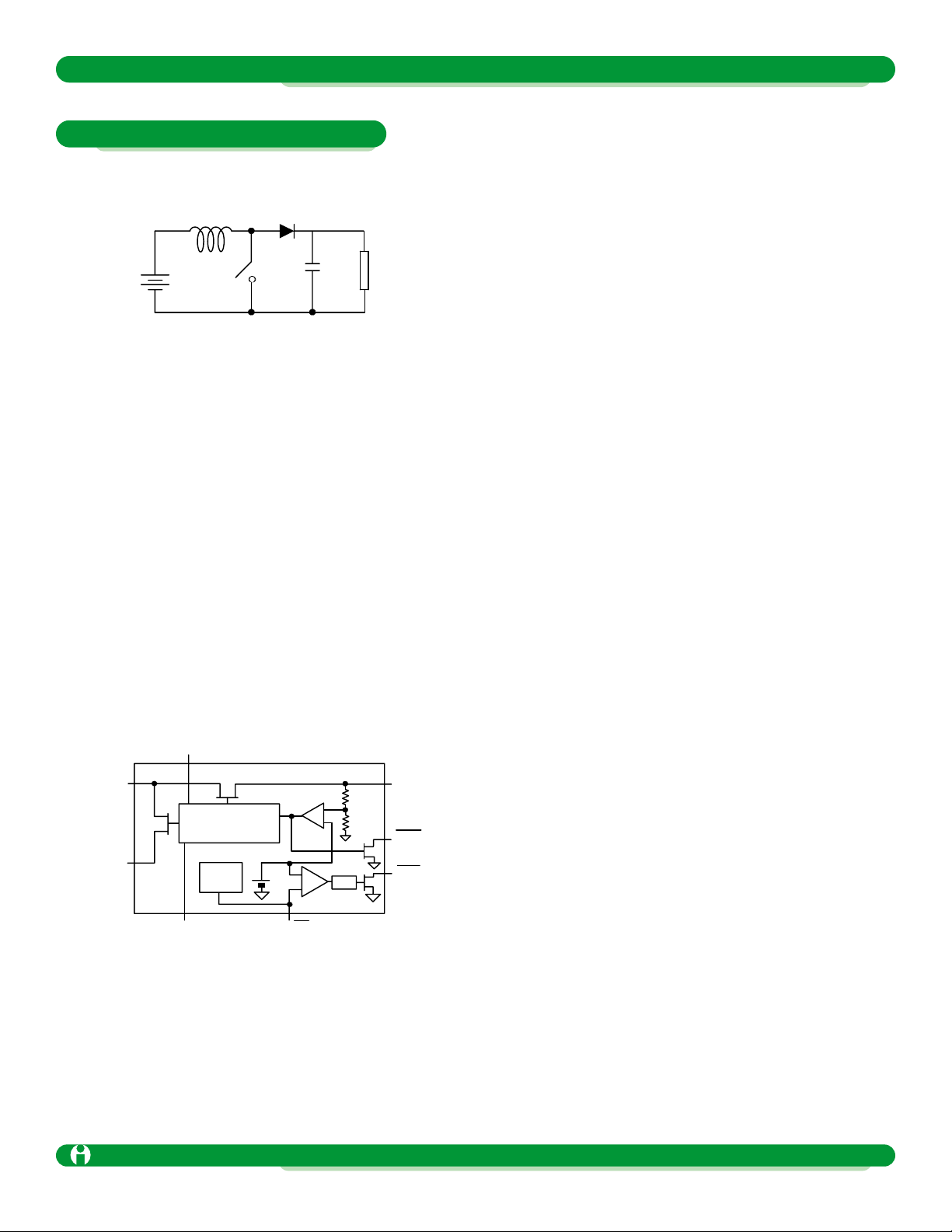
The ILC6360 performs both buck and boost DC-DC conversion by controlling the switch element as shown in the
simplified circuit in figure 1 below.
When the switch is closed, current is built up through the
inductor. When the switch opens, this current is forced
through the diode to the output capacitor and load. As this
on and off switching continues, the output capacitor voltage
builds up due to the charge it is storing from the inductor
current. The output voltage is therefore boosted relative to
the input.
In general, the switching characteristic is determined by the
output voltage desired and the current required by the load.
Specifically the energy transfer is determined by the power
stored in the coil during each switching cycle.
P
L
= ƒ(tON, VIN)
Synchronous Rectification
The ILC6360 also uses a technique called “synchronous
rectification” which removes the need for the external diode
used in other circuits. The diode is replaced with a second
switch (SW2) or in the case of the ILC6360, a FET as
shown in figure 2 below.
The two switches now open and close in opposition to each
other, directing the flow of current to either charge the
inductor or to feed the load. The ILC6360 monitors the voltage on the output capacitor to determine how much and
how often to drive the switches.
Modes of Operation
There are four modes of operation for the ILC6360
buck/boost DC-DC converter. These four modes are internally selected by the regulator depending on external conditions such as line voltage, output voltage, load current,
inductor size, output capacitor size and resistive losses.
The first mode is the discontinuous mode. If the load is light
and the inductor value is small enough, the inductor will
transfer all of its energy to the output capacitor before a
cycle is completed. The input current waveform instead of
being continuous with a triangle ripple, will be a series of
discrete triangle shaped pulses as the inductor charges
from the input and discharges into the capacitor. The ripple
on the output capacitor becomes larger than expected compared to continuous mode calculation because of the current spikes from the input.
Boost (Step-up) Operation
The second mode is the conventional boost (step-up) mode
of operation. The input current is a smooth waveform with a
triangular ripple current. The output waveform exhibits ripple caused by the charging and discharging of the output
capacitor and the current flowing through the capacitor’s
equivalent series resistance (ESR).
The third mode is the PFM mode. If the output voltage
exceeds an upper limit, for whatever reason, the regulator
enters the PFM mode. The regulator shuts down for one or
more cycles until the output voltage drops below a pre-set
threshold and one cycle is initiated. The inductor current falls
to zero during the off time. The basic cycle is the 3.3mS
PWM cycle but one or more cycles are dropped from the
pulse train (also called pulse skipping). This may be in
response to a light load condition or from a fast transient
load condition where the output capacitor charges too high
during load turn-off. In light load conditions, PFM mode
offers high efficiency due to significantly lower quiescent current for the regulator. The output voltage will be a few tens
of millivolts higher in the PFM mode than in the PWM mode.
The fourth mode of operation is the buck (step-down) mode
and is described below.
Buck (Step-down) Operation
The “buck” mode is not a true switching regulator mode but
allows the regulator to operate when the input voltage
exceeds the output voltage. Once the input voltage exceeds
the output voltage, the regulator is not capable of limiting
the current in a non-dissipative fashion.
Fig. 1: Basic Circuit
V
OUT
POK
LBO
LB/SD
SYNC
GND
L
X
V
IN
ILC6360
PWM/PFM
CONTROLLER
SHUTDOWN
CONTROL
V
REF
DELAY
+
+
-
-
SW2
SW1
Fig. 2: Simplified ILC6360 block diagram
APPLICATIONS INFORMATION
 Loading...