Impala Linear Corporation ILC1232N, ILC1232M Datasheet

ILC1232
Impala Linear Corporation
1
mP Supervisory Circuit
(408) 574-3939
www.impalalinear.com
Sept 1999
Impala Linear Cor poration
ILC1232 1.1
1
The ILC1232 is a multifunction circuit which monitors microprocessor activity, external reset and power supplies in
microprocessor based systems. The circuit functions
include a watchdog timer, power supply monitor, microprocessor reset, and manual pushbutton reset input.
The power supply line is monitored with a comparator and
an internal voltage reference. RST is forced low when an
out-of-tolerance condition exists and remains asserted for
at least 250ms after V
CC
rises above the threshold voltage
(4.5V or 4.75V). The RST pin will remain logic low with V
CC
as low as 1.4V.
The Watchdog input (ST) monitors mP activity and will
assert RST if no mP activity has occurred within the watchdog timeout period. The watchdog timeout period is selectable with nominal periods of 150, 600, or 1200 milliseconds.
• Power OK/Reset Time Delay, 250ms min.
• Watchdog Timer, 150ms, 600ms, or 1.2s typical
• Precision Supply Voltage Monitor, Select Between 5% or
10% of Supply Voltage
• 18µA Supply Current
• Debounced External Reset Input
• 8-Pin SO Package
• Computers
• Controllers
• Critical Microprocessor Power Monitoring
• Intelligent Instruments
• Portable Equipment
ILC1232
VCC
Top View
PBRST
RST
TD
2
1 8
6
RST
GND
ST
TOL
4
3
5
7
ETC1232N - 8 Lead Plastic DIP Package
ETC1232M - 8 Lead Plastic SOIC Package
Part Package Temp. Range
ILC1232N 8-Lead PDIP -40°C to +85°C
ILC1232M 8-Lead SOIC -40°C to +85°C
Ordering Information
ILC1232
µµ
P
VCC
VCC
VCC
ST
RESET
PBRST
RST
TD
GND
TOL
I/O
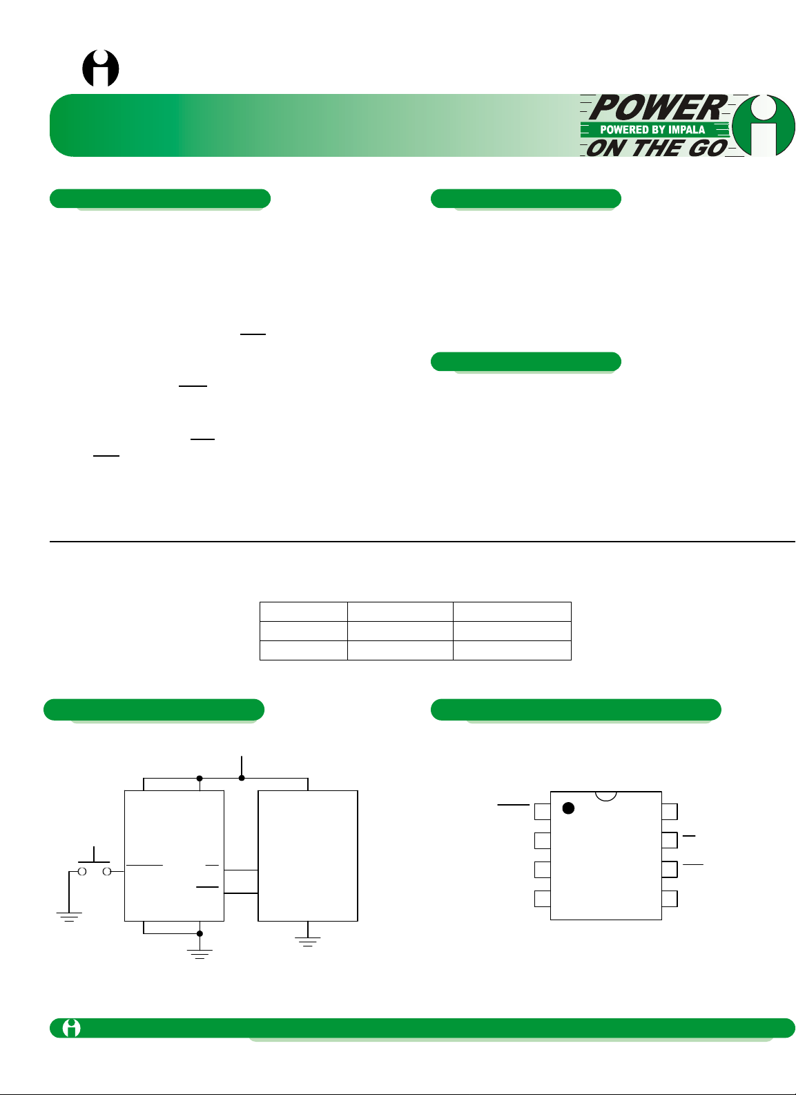
Typical Circuit
Pin Package Configurations
General Description
Features
Applications

Parameter Symbol Ratings Units
V
CC
-0.3 to 6.0 VTerminal Voltage
All other inputs
-0.3 to (VCC + 0.3)
V
Input Current V
CC
250 mA
GND, All other
inputs
25 mA
Operating Temperature Range T
A
-40 to +85 °C
Storage Temperature Range -65 to +150 °C
Lead Temperature (Soldering, 10 sec.) 300 °C
Power Dissipation 700 mW
Stresses above those listed under ABSOLUTE MAXIMUM RATINGS may cause permanent device failure. Functionality at
or above these limits is not implied. Exposure to absolute maximum ratings for extended periods may affect device reliability. Operating ranges define those limits between which the functionality of the device is guaranteed.
VCC = 4.5 V to 5.5 V, TA = Operating Temperature Range, unless ot herwise noted.
Parameter
Conditions
Min
Typ
Max
Units
Operating Voltage Range, VCC
4.5 5.5
V
Supply Current, ICC
(See Note 1)
18
40
µA
ST and PBRST Input Levels
VIH (See Note 2)
VIL
2.0
-0.3
VCC + 0.3
0.8
V
Input Leakage, IIL
1
µA
Output Source Current, RST
VOH = 2.4V
1.0
10 mA
Output Sink Current, RST, RST
VOL = 0.4V
2.0
10 mA
VCC 5% Trip Point (Reset Threshold Vol tage)
TOL= GND
4.50
4.62
4.74
V
VCC 10% Trip Point (Reset Threshold V ol t age)
TOL= VCC
4.25
4.37
4.49
V
Input Capacitance, ST, TOL
CIN (See Note 3)
5
pF
Output Capacitance, RST, RS T
C
OUT
(See Note 3)
7
pF
PBRST Min. Pulse Width, tPB
PBRST = VIL (See Note 4)
20
ms
PBRST Delay, t
PBD
1 4
20
ms
Reset Active Time, t
RST
250
610
1000
ms
ST Pulse W i dt h, tST
20
ns
ST Timeout Period, tTD
TD = 0V
TD = Open
TD = VCC
62.5
250
500
150
600
1200
250
1000
2000
ms
VCC Fall Time, tF
10
µs
VCC Rise Time, tR
0 ns
VCC Detect to RST Low and RST High, tRPD
VCC Falling at 1.66 mV/µs
50
150
µs
VCC Detect to RST Open and RST Low, tRPU
VCC Rising (See Note 5)
250
610
1000
ms
Note 1: ICCis measured with outputs open and inputs within 0.5V of supply rails.
Note 2: PBRST has an internal 40kΩ (typical) pull-up resistor to VCC.
Note 3: Guaranteed by design.
Note 4: PBRST must be held low for a minimum of 20ms to guarantee a reset.
Note 5: RST has an open drain output.
ILC1232 mP Supervisory Circuit
Sept 1999
Impala Linear Corporation
2
(408) 574-3939
www.impalalinear.com
ILC1232 1.1
June 1999
Absolute Maximum Ratings
Electrical Characterisitcs
 Loading...