


IMP IMP708SESA, IMP708SCUA, IMP708SCSA, IMP708SCPA, IMP708RESA Datasheet
...
©
1999 IMP, Inc. 408-432-9100/www.impweb.com
1
Key Features
Applications
◆ Computers and controllers
◆ CTI applications
◆ Embedded controllers
◆ Battery operated systems
◆ Intelligent instruments
◆ Wireless communication systems
◆ PDAs and handheld equipment
◆
Lower power, pin compatible replacements for
Maxim MAX706P/R/S/T, MAX708R/S/T
– 30% lower supply current:140µA vs. 200µA
◆
Precision power supply monitor
– 2.63V threshold (IMP706P/R, IMP708R)
– 2.93V threshold (IMP706S, IMP708S)
– 3.08V threshold (IMP706T, IMP708T)
– New 4.00V threshold (IMP706J, IMP708J)
◆
Debounced manual reset input
◆
Auxiliary voltage monitor comparator
– 1.25V threshold
– Battery monitor/auxiliary supply monitor
◆
Watchdog timer (IMP706P/R/S/T/J)
– Watchdog can be disabled by floating WDI
◆
200ms reset time delay
◆
Three reset signal options
– Active HIGH: IMP706P
– Active LOW: IMP706R/S/T/J
– Active HIGH & LOW outputs: IMP708R/S/T/J
◆
DIP, SO and MicroSO packages
◆
Guaranteed RESET assertion to VCC= 1.1V
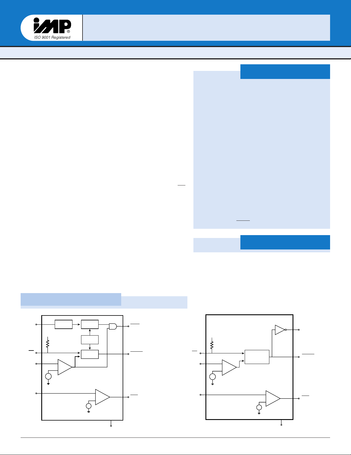
Block Diagrams
IMP706P/R/S/T/J, IMP708R/S/T/J
IMP706P/R/S/T/J, IMP708R/S/T/J
POWER MANAGEMENT
3/3.3/4.0V
3/3.3/4.0V µµ
P Super
P Super
visor Cir
visor Cir
cuits
cuits
– Lo
– Lo
w suppl
w suppl
y cur
y currr
ent
ent
– W
– W
atc
atc
hdog timer
hdog timer
– Br
– Broo
wnout det
wnout det
ection
ection
The IMP706P/R/S/T/J and IMP708R/S/T/J CMOS supervisor circuits
monitor power-supply and battery voltage level, and µP/µC operation.
A reset is generated when the supply drops below 2.63V (IMP706P/R,
IMP708R), 2.93V (IMP706S, IMP708S), 3.08V (IMP706T, IMP708T) or 4.00
(IMP706J, IMP708J).
The family offers several functional options. Each device generates a
reset signal during power-up, power-down and during brownout
conditions.
In addition, the IMP706P/R/S/T/J feature a 1.6 second watchdog timer.
The watchdog timer output will trigger a reset if connected to MR.
Unlike competitive devices, floating the WDI input pin disables the
watchdog timer.
The IMP708R/S/T/J have both active-HIGH and active-LOW reset outputs but no watchdog function. The IMP706P has the same pin-out and
functions as the IMP706R but has an active-HIGH reset output.
A versatile power-fail circuit, useful in checking battery levels and
non-5V supplies, has a 1.25V threshold. All devices have a manual
reset input.
All devices are available in 8-pin DIP, SO and the compact MicroSO
packages. The MicroSO package requires 50% less PC board area than
the conventional SO package.
WDI
MR
V
PFI
V
CC
20kΩ
CC
+
IMP706P/R/S/T/J
Transition
Detector
+
–
2.63V (IMP706P/R)
2.93V (IMP706S)
3.08V (IMP706T)
4.00V (IMP706J)
Watchdog
Timebase
Generator
1.25V
Timer
RESET
WDO
RESET
(RESET) IMP706P
+
–
GND
PFO
706P_01.eps
V
CC
20kΩ
V
MR
PFI
CC
+
+
–
2.63V (IMP708R)
2.93V (IMP708S)
3.08V (IMP708T)
4.00V (IMP708J)
IMP708R/S/T/J
RESET
Generator
1.25V
RESET
RESET
+
–
GND
PFO
706P_02.eps
2
408-432-9100/www.impweb.com
©
1999 IMP, Inc.
Ordering Information
Pin Configuration
IMP706P/R/S/T/J, IMP708R/S/T/J
IMP706P/R/S/T/J, IMP708R/S/T/J
IMP708R/S/T/J
1
2
3
4
MR
V
CC
GND
PFI
RESET
RESET
NC
PFO
8
7
6
5
IMP706P
1
2
3
4
MR
V
CC
GND
PFI
WDO
RESET
WDI
PFO
8
7
6
5
IMP706R/S/T/J
1
2
3
4
MR
V
CC
GND
PFI
WDO
RESET
WDI
PFO
8
7
6
5
IMP706P
IMP706R/S/T/J
1
2
3
4
(RESET) RESET
(IMP706P)
WDO
MR
V
CC
WDI
PFO
PFI
GND
8
7
6
5
IMP708R/S/T/J
1
2
3
4
RESET
RESET
MR
V
CC
NC
PFO
PFI
GND
8
7
6
5
706P_03.eps
DIP/SO
MicroSO
Operating
Part Number Package Temperature Range Reset Threshold Reset Polarity Watchdog Timer
IMP706PCPA 8-Plastic DIP 0°C to +70°C 2.63 HIGH YES
IMP706PCSA 8-SO 0°C to +70°C 2.63 HIGH YES
IMP706PCUA 8-MicroSO 0°C to +70°C 2.63 HIGH YES
IMP706PEPA 8-Plastic DIP –40°C to +85°C 2.63 HIGH YES
IMP706PESA 8-SO –40°C to +85°C 2.63 HIGH YES
IMP706RCPA 8-Plastic DIP 0°C to +70°C 2.63 LOW YES
IMP706RCSA 8-SO 0°C to +70°C 2.63 LOW YES
IMP706RCUA 8-MicroSO 0°C to +70°C 2.63 LOW YES
IMP706REPA 8-Plastic DIP –40°C to +85°C 2.63 LOW YES
IMP706RESA 8-SO –40°C to +85°C 2.63 LOW YES
IMP706SCPA 8-Plastic DIP 0°C to +70°C 2.93 LOW YES
IMP706SCSA 8-SO 0°C to +70°C 2.93 LOW YES
IMP706SCUA 8-MicroSO 0°C to +70°C 2.93 LOW YES
IMP706SEPA 8-Plastic DIP –40°C to +85°C 2.93 LOW YES
IMP706SESA 8-SO –40°C to +85°C 2.93 LOW YES
IMP706TCPA 8-Plastic DIP 0°C to +70°C 3.08 LOW YES
IMP706TCSA 8-SO 0°C to +70°C 3.08 LOW YES
IMP706TCUA 8-MicroSO 0°C to +70°C 3.08 LOW YES
IMP706TEPA 8-Plastic DIP –40°C to +85°C 3.08 LOW YES
IMP706TESA 8-SO –40°C to +85°C 3.08 LOW YES
IMP706JCPA 8-Plastic DIP 0°C to +70°C 4.00 LOW YES
IMP706JCSA 8-SO 0°C to +70°C 4.00 LOW YES
IMP706JCUA 8-MicroSO 0°C to +70°C 4.00 LOW YES
IMP706JEPA 8-Plastic DIP –40°C to +85°C 4.00 LOW YES
IMP706JESA 8-SO –40°C to +85°C 4.00 LOW YES
IMP708RCPA 8-Plastic DIP 0°C to +70°C 2.63 Dual: HIGH & LOW NO
IMP708RCSA 8-SO 0°C to +70°C 2.63 Dual: HIGH & LOW NO
IMP708RCUA 8-MicroSO 0°C to +70°C 2.63 Dual: HIGH & LOW NO
IMP708REPA 8-Plastic DIP –40°C to +85°C 2.63 Dual: HIGH & LOW NO
IMP708RESA 8-SO –40°C to +85°C 2.63 Dual: HIGH & LOW NO
IMP708SCPA 8-Plastic DIP 0°C to +70°C 2.93 Dual: HIGH & LOW NO
IMP708SCSA 8-SO 0°C to +70°C 2.93 Dual: HIGH & LOW NO
IMP708SCUA 8-MicroSO 0°C to +70°C 2.93 Dual: HIGH & LOW NO
IMP708SEPA 8-Plastic DIP –40°C to +85°C 2.93 Dual: HIGH & LOW NO
IMP708SESA 8-SO –40°C to +85°C 2.93 Dual: HIGH & LOW NO
IMP708TCPA 8-Plastic DIP 0°C to +70°C 3.08 Dual: HIGH & LOW NO
IMP708TCSA 8-SO 0°C to +70°C 3.08 Dual: HIGH & LOW NO
IMP708TCUA 8-MicroSO 0°C to +70°C 3.08 Dual: HIGH & LOW NO
IMP708TEPA 8-Plastic DIP –40°C to +85°C 3.08 Dual: HIGH & LOW NO
IMP708TESA 8-SO –40°C to +85°C 3.08 Dual: HIGH & LOW NO
IMP708JCPA 8-Plastic DIP 0°C to +70°C 4.00 Dual: HIGH & LOW NO
IMP708JCSA 8-SO 0°C to +70°C 4.00 Dual: HIGH & LOW NO
IMP708JCUA 8-MicroSO 0°C to +70°C 4.00 Dual: HIGH & LOW NO
IMP708JEPA 8-Plastic DIP –40°C to +85°C 4.00 Dual: HIGH & LOW NO
IMP708JESA 8-SO –40°C to +85°C 4.00 Dual: HIGH & LOW NO
Pin Terminal Voltage with Respect to Ground
V
CC
. . . . . . . . . . . . . . . . . . . . . . . . . . . . . . . . . –0.3V to 6.0V
All other inputs . . . . . . . . . . . . . . . . . . . . . . . . – 0.3V to (V
CC
+ 0.3V)
Input Current at V
CC
and GND . . . . . . . . . . 20mA
Output Current: All outputs . . . . . . . . . . . . . 20mA
Rate of Rise at V
CC
. . . . . . . . . . . . . . . . . . . . . 100V/µs
Plastic DIP Power Dissipation . . . . . . . . . . . 700mW
(Derate 9mW/°C above 70°C)
SO Power Dissipation . . . . . . . . . . . . . . . . . . 470mW
(Derate 5.9mW/°C above 70°C)
MicroSO Power Dissipation . . . . . . . . . . . . . 330mW
(Derate 4.1mW/°C above 70°C)
Operating Temperature Range
IMP706xE, IMP708xE . . . . . . . . . . . . . . . . . . – 40°C to +85°C
IMP706xC, IMP708xC . . . . . . . . . . . . . . . . . . 0°C to +70°C
Storage Temperature Range . . . . . . . . . . . . . . –65°C to +160°C
Lead Temperature Soldering (10 sec) . . . . . . 300°C
These are stress ratings only and functional operation is not implied.
Exposure to absolute maximum ratings for prolonged time periods may
affect device reliability.
©
1999 IMP, Inc. 408-432-9100/www.impweb.com
3
IMP706P/R/S/T/J, IMP708R/S/T/J
IMP706P/R/S/T/J, IMP708R/S/T/J
Absolute Maximum Ratings
Electrical Characteristics
Unless otherwise noted, specifications are over the operating temperature range and VCCsupply voltages are 2.7V to 5.5V (IMP706P,
IMP708R), 3.0V to 5.5V (IMP706/8S), 3.15V to 5.5V (IMP706/8T) and 4.1V to 5.5V (IMP706/8J).
retemaraPlobmySsnoitidnoCniMpyTxaMstinU
egatloVgnitarepO
egnaR
V
CC
Cx807PMI,Cx607PMI
Ex807PMI,Ex607PMI
1.1
2.1
5.5
5.5
V
tnerruCylppuS
V
CC
V6.3<
I
CC
V=RM,Ex607PMI,Cx607PMI
CC
gnitaolFIDW,57041
µA
V=RM,Ex807PMI,Cx807PMI
CC
gnitaolFIDW,05041
tnerruCylppuS
V
CC
V5.5<
I
CC
V=RM,Ex607PMI,Cx607PMI
CC
gnitaolFIDW,57041
µA
V=RM,Ex807PMI,Cx807PMI
CC
gnitaolFIDW,05041
dlohserhTTESERV
TR
secivedRdnaP
secivedS
secivedT
secivedJ
55.2
58.2
00.3
98.3
36.2
39.2
80.3
00.4
07.2
00.3
51.3
01.4
V
dlohserhTTESER
siseretsyH
04Vm
htdiWesluPTESERt
SR
V
CC
,)secivedR/P,8/607PMI(V3=
V
CC
)secivedT/S,8/607PMI(V3.3=
V
CC
)secivedJ,8/607PMI(V4.4=
041002082sm
V
CC
V5=002
htdiWesluPRMt
RM
V<V5.4
CC
V5.5<051sn
V<V6.3
CC
)secivedJ8/607PMI(V5.4<
V
)XAM(TSR
V<
CC
)secivedT/S/R/P8/607PMI(V6.3<
005
yaleDtuOTESERotRMt
DM
V<V6.3
CC
)secivedJ8/607PMI(V5.4<
V
)XAM(TSR
V<
CC
)secivedT/S/R/P8/607PMI(V6.3<
057sn
V<V5.4
CC
V5.5<052
dlohserhTtupnIRMV
HI
V
)XAM(TSR
V<
CC
V5.4<V7.0
CC
V
V
LI
V
)XAM(TSR
V<
CC
V5.4<6.0
V
HI
V<V5.4
CC
V5.5<0.2
V
LI
V<V5.4
CC
V5.5<8.0
rotsiseRpu-lluPRMR
P
010204kΩ
egatloVtuptuOTESER
)secivedJ/T/S/RllA(
V
HO
I
ECRUOS
008= µ V<V5.4,A
CC
V5.5<V
CC
V5.1– V
V
LO
I
KNIS
V<V5.4,Am2.3=
CC
V5.5<4.0
V
HO
I
ECRUOS
005= µ V,A
)XAM(TSR
V<
CC
V5.4<V8.0
CC
V
LO
I
KNIS
V,Am2.1=
)XAM(TSR
V<
CC
V5.4<3.0
V
LO
I
KNIS
05= µ V,A
CC
)secivedCx807PMI,Cx607PMI(V1.1=3.0
I
KNIS
001= µ V,A
CC
)secivedEx807PMI,Ex607PMI(V2.1=3.0