

IMP IMP528ESA, IMP528EMA Datasheet
© 2001 IMP, Inc. 408-432-9100/www.impweb.com 1
IMP528
IMP528
POWER MANAGEMENT
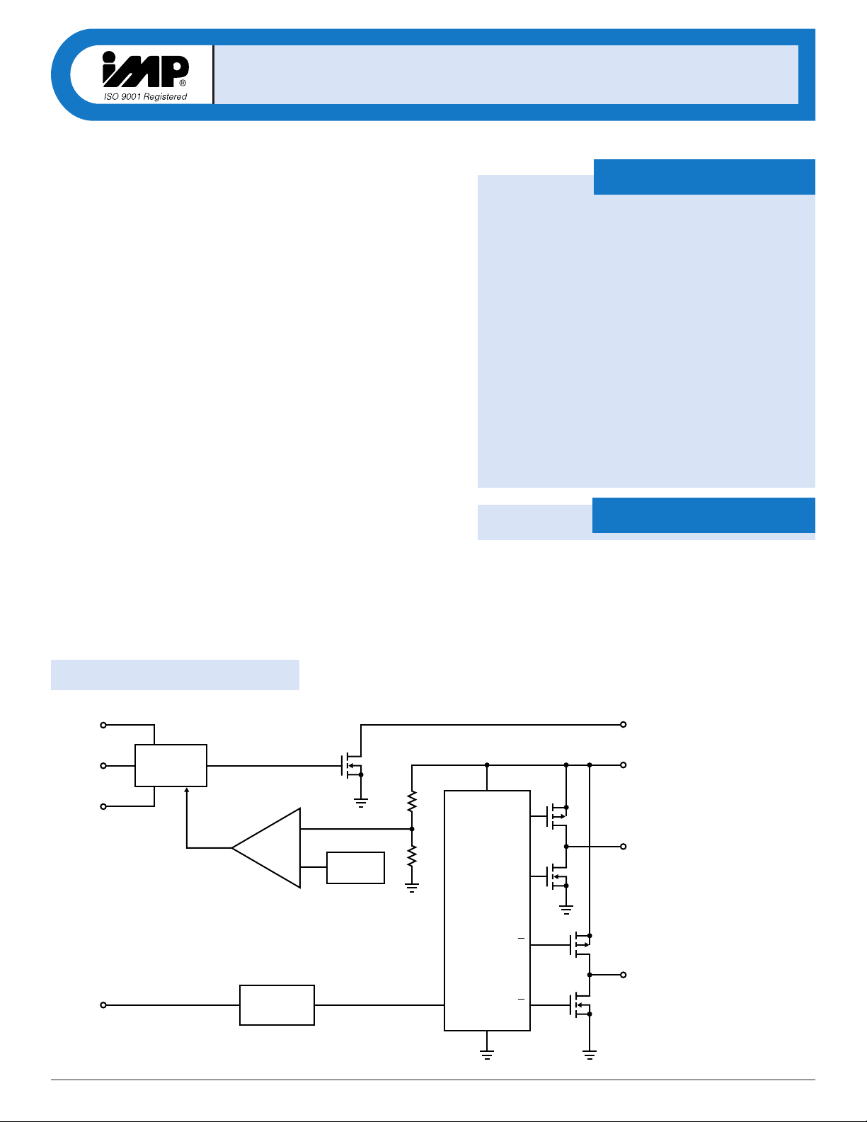
Block Diagram
High-
High-VV
olt
olt
ag
ag
e EL Lam
e EL Lam
p Dr
p Driviverer
– 220 V
– 220 V
PP
PP
DrDrivive
e
◆ GPS units/Pagers/Cellular phones
◆ PDAs/Handheld computers
◆ Safety illumination
◆ Portable instrumentation
◆ Battery-operated displays
◆ LCD modules
◆ Toys
◆ 220V peak-to-peak typical AC output voltage
◆ Low Power: 420µA typical V
DD
current
◆ Wide operating voltage range -from 2.0V to 6.5V
◆ Large output load capability - drives lamps
with more than 50nF capacitance
◆ Eliminates external protection resistor in series
with EL lamp
◆ Adjustable output lamp frequency for control of
lamp color, lamp life, and power consumption
◆ Adjustable converter frequency to minimize
power consumption
◆ High-Voltage CMOS Process
◆ MicroSO package option
Key Features
Applications
–
+
528_01.eps
V
DD
1
L
X
4
C
S
3
V
A
7
V
B
6
R
SW-OSC
2
Switch
Oscillator
Regulation
Control
IMP528
Bridge
Output
Driver
Q
Q
Q
V
REF
Lamp Drive
Oscillator
C
GND
5
R
EL-OSC
8
Q
The IMP528 is an Electroluminescent (EL) lamp driver with the four EL
lamp driving functions on-chip. These are the switch-mode power supply, its high-frequency oscillator, the high-voltage H-bridge lamp driver
and its low-frequency oscillator. The IMP528 drives EL lamps of up to
50nF capacitance to high brightness; EL lamps with capacitances greater
than 50nF can be driven, but will be lower in light output. The typical
regulated output voltage that is applied to the EL lamp is 220V peak-topeak. The circuit requires few external components; a single inductor,
single diode, two capacitors and two resistors. Two of these resistors
set the frequency for two internal oscillators.
Unlike other EL lamp drivers, the IMP528 does not require an external
protection resistor in series with the EL lamp.
The IMP528 operates over a 2.0V to 6.5V supply voltage range. A
regulated, low-power source can supply the low quiescent current of the
IMP528. The inductor may be driven from an independent, unregulated
supply voltage in dual supply applications.
An internal circuit shuts down the switching regulator when the lamp
drive voltage reaches 220V peak-to-peak. This conserves power and
extends battery life.
The IMP528 is available in MicroSO and SO-8 packages and in die or
wafer form.
IMP528
IMP528
2 408-432-9100/www.impweb.com © 2001 IMP, Inc.
Electrical Characteristics
Absolute Maximum Ratings
Ordering Information
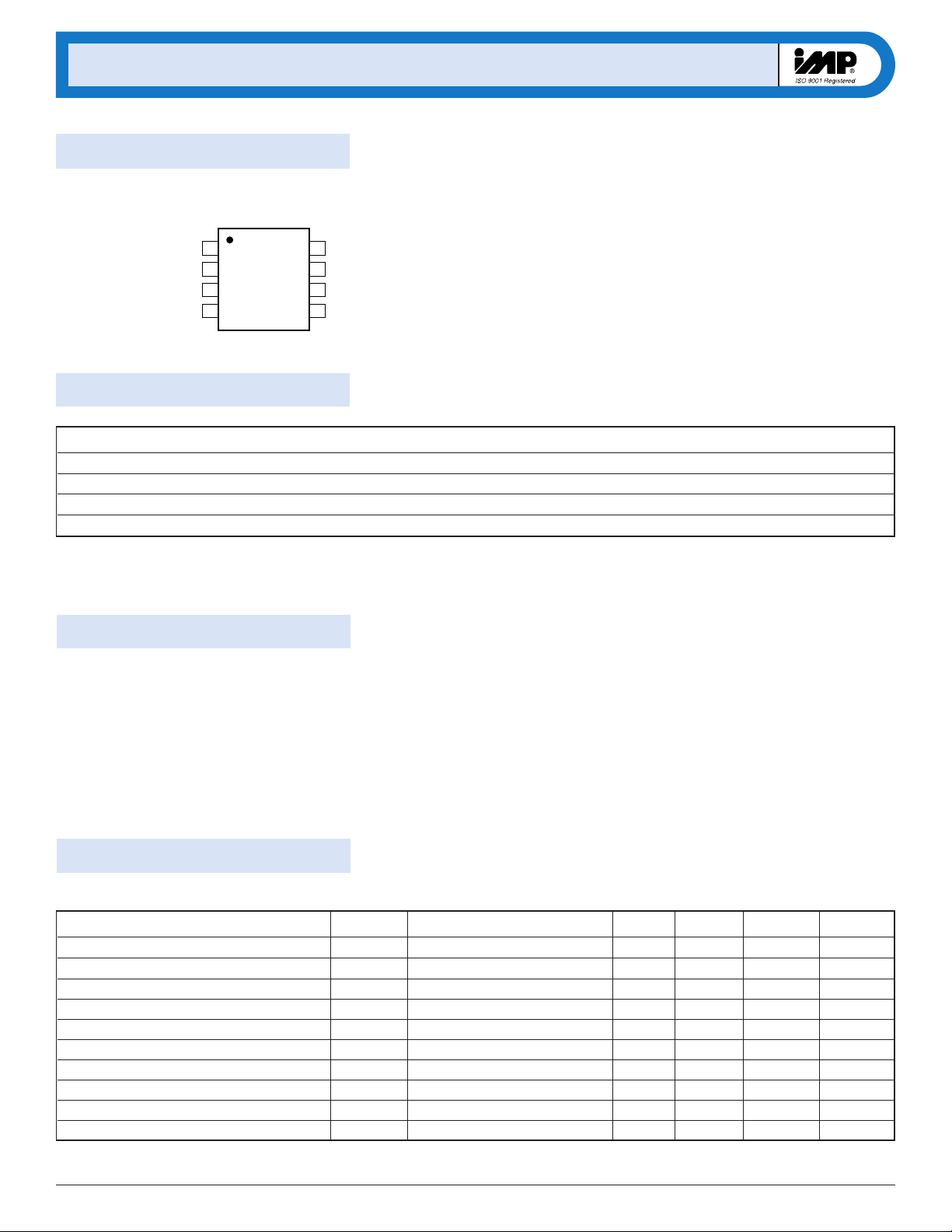
Pin Configuration
Parameter Symbol Conditions Min Typ Max Units
ON-resistance of MOS Switch R
DS(ON)
I = 100mA 3.0 8 Ω
Output Voltage Regulation V
CS
VDD= 2.0 to 6.5V 110 V
Output Voltage Peak-to-peak (in regulation) VA-V
B
VDD= 2.0 to 6.5V 220 V
Input Current at VDDPin I
DD
VDD= 3.0V, See Figure 1 420 700 µA
Input Current at VDDPin I
DD
VDD= 5.0V 500 750 µA
Quiescent VDDSupply Current, Disabled I
DDQ
V
RSW-OSC
< 100mV 20 200 nA
Input Current: IDDPlus Inductor Current I
IN
VDD= 3.0V, See Figure 1 21 31 mA
V
A-B
Output Drive Frequency f
EL
VDD= 3.0V, See Figure 1 250 Hz
Switching Frequency f
SW
VDD= 3.0V, See Figure 1 61 kHz
Switching Duty Cycle D
SW
VDD= 3.0V, See Figure 1 88 %
4L
X
3C
S
2R
SW-OSC
1V
DD
5 GND
6V
B
7V
A
8R
EL-OSC
528_02.eps
IMP528
SO/ MicroSO
Part Number Input Voltage Regulated Output Voltage Temperature Range Pins-Package
IMP528ESA 2.0V to 6.5V Yes – 40°C to +85°C 8-SO
IMP528EMA 2.0V to 6.5V Yes – 40°C to +85°C 8-MicroSO
IMP528/D* 2.0V to 6.5V Yes 25°C Dice
IMP528/D1** 2.0V to 6.5V Yes 25°C Dice
VDD . . . . . . . . . . . . . . . . . . . . . . . . . . . . . . . . . . –0.5V to +7.0V
V
RSW-OSC
and V
REL-OSC
. . . . . . . . . . . . . . . . . . . –0.5V to V
DD
+0.3V
V
CS
, LX . . . . . . . . . . . . . . . . . . . . . . . . . . . . . . . . –0.5V to +120V
Operating Temperature Range . . . . . . . . . . . . –40°C to +85°C
Storage Temperature Range . . . . . . . . . . . . . . –65°C to +150°C
Power Dissipation (SO) . . . . . . . . . . . . . . . . . . 400mW
Power Dissipation (MicroSO) . . . . . . . . . . . . . 300mW
V
A
, VB . . . . . . . . . . . . . . . . . . . . . . . . . . . . . . . . –0.5V to VCS(pin 3)
Unless otherwise noted, VDD= 3.0V, RSW= 910kΩ, REL= 2.7MΩ, and TA= 25°C.
Note: All voltages are referenced to GND.
These are stress ratings only and functional operation is not
implied. Exposure to absolute maximum ratings for prolonged
time periods may affect device reliability.
Pin Compatible With IMP803 and IMP560
* Disable pad not active
** Disable pad active
Add /T to ordering part number for Tape and Reel.
 Loading...