

IMP IMP525EMA Datasheet
© 2000 IMP, Inc. 408-432-9100/www.impweb.com 7
IMP525
IMP525
POWER MANAGEMENT
Sing
Sing
le Cell Batt
le Cell Batt
er
er
y P
y Pooww
er
er
ed
ed
Electr
Electr
oluminescent Lam
oluminescent Lampp
Dr
Driviv
er/In
er/Invv
er
ertt
er
er
◆ Audio/TV remote control units
◆ Pagers/Cellular phones
◆ PDAs
◆ Clocks and radios
◆ Portable GPS receivers
◆ LCD modules
◆ Toys
◆ Wide operating voltage range - from 0.9V to 2.5V
◆ Simple design requires few passive components
◆ 112V peak-to-peak typical AC output voltage
◆ Adjustable output frequency controls lamp
color and power consumption
◆ Adjustable converter frequency minimizes
circuit power consumption
◆ Disable mode extends battery life
◆ Disable current 1µA typical
◆ Compact MicroSO package option
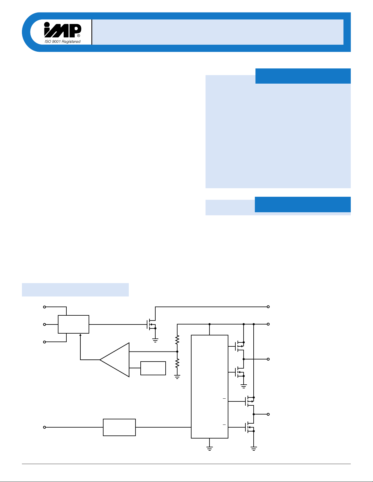
Block Diagram
–
+
525_01.eps
V
DD
1
L
X
4
C
S
3
V
A
7
V
B
6
R
SW-OSC
2
Switch
Oscillator
Regulation
Control
IMP525
Bridge
Output
Driver
Q
Q
Q
V
REF
Lamp Drive
Oscillator
C
GND
5
R
EL-OSC
8
Q
The IMP525 is an Electroluminescent (EL) lamp driver designed for systems that must operate down to 1 volt and below. The input supply voltage range is 0.9V to 2.5V. Typical output lamp drive voltage is 112V. All
four EL lamp-driving functions are on-chip. These are the switch-mode
power supply, its high-frequency oscillator, the high-voltage H-bridge
lamp driver and its low-frequency oscillator. EL lamps of up to 6nF
capacitance can be driven to high brightness.
The circuit requires few external components; one inductor, one diode,
one capacitor and two resistors. The resistors set the frequency for the
two oscillators.
A disable mode puts the chip into a low current-drain state. When disabled, quiescent current drops to 1µA typical with a V
DD
of 1.5V. The chip
can be disabled by connecting R
SW
, the oscillator frequency setting
resistor, to ground. A disable pad (active low), accessible only on the die,
can also be used to disable the driver.
An internal circuit shuts down the switching regulator when the lamp
drive voltage exceeds 112V peak-to-peak. This conserves power and
extends battery life.
The IMP525 is available in MicroSO and SO-8 packages and in die form.
Key Features
Applications
IMP525
IMP525
8 408-432-9100/www.impweb.com © 2000 IMP, Inc.
Parameter Symbol Conditions Min Typ Max Units
ON-resistance of MOS Switch R
DS(ON)
I = 50mA 15 Ω
Operating Voltage 0.9 2.5 V
Output Voltage at C
S
V
CS
VDD= 1.5V, See Figure 1, Table 1 52 58 65 V
Output Voltage at C
S
V
CS
VDD= 0.9V, See Figure 1, Table 2 50 V
Output Voltage Peak-to-Peak VA-V
B
V
DD
= 1.5V, See Figure 1 104 112 124 V
P-P
Quiescent VDDSupply Current, Disabled I
QDIS
Disable = HIGH 70 nA
(Disable pin available on die only)
Quiescent V
DD
Supply Current, Disabled I
QDIS
R
SW-OSC
= GND 1.0 2.0 µA
VDD= 1.5V
Input Current at VDDPin I
DD
VDD= 0.9V to 1.5V 1.5 mA
Input Current: IDDPlus Inductor Current I
IN
VDD= 1.5V 23 32 mA
V
A-B
Output Drive Frequency f
EL
VDD= 1.5V, See Figure 1, Table 1 500 Hz
Boost Converter Switching Frequency f
SW
VDD= 1.5V, See Figure 1, Table 1 26 kHz
Switching Duty Cycle D
SW
VDD= 1.5V, See Figure 1 87.5 %
Disable Input LOW Voltage V
DISL
GND 0.2 V
(Disable pin available on die only)
Disable Input HIGH Voltage V
DISH
VDD-0.5V V
DD
V
(Disable pin available on die only)
Ordering Information
Pin Configuration
4L
X
3C
S
2R
SW-OSC
1V
DD
5 GND
6V
B
7V
A
8R
EL-OSC
525_02.eps
IMP525
SO/MicroSO
Part Number Input Voltage Regulated Output Voltage Temperature Range Pins-Package
IMP525EMA 0.9V to 2.5V YES – 40°C to +85°C 8-MicroSO
IMP525ESA 0.9V to 2.5V YES – 40°C to +85°C 8-SO
IMP525/D* 0.9V to 2.5V YES 25°C Dice
IMP525/D1** 0.9V to 2.5V YES 25°C Dice
Absolute Maximum Ratings
Supply Voltage, VDD, V
RSW-OSC
and V
REL-OSC
. . – 0.5V to +3.5V
Storage Temperature Range . . . . . . . . . . . . . . . . – 65°C to +150°C
Power Dissipation (SO package) . . . . . . . . . . . . 400mW
Power Dissipation (MicroSO package) . . . . . . . 300mW
Unless otherwise noted, V
DD
= 1.5V, RSW= 1MΩ, REL= 1.0MΩ, and TA= 25°C.
Note: All voltages are referenced to GND.
These are stress ratings only and functional operation is not implied.
Exposure to absolute maximum ratings for prolonged time periods may
affect device reliability.
Electrical Characteristics
* Disable pad not active
** Disable pad active
Add /T to ordering part number for Tape and Reel.
IMP525
IMP525
© 2000 IMP, Inc.
Electroluminescent Lamp Driver
9
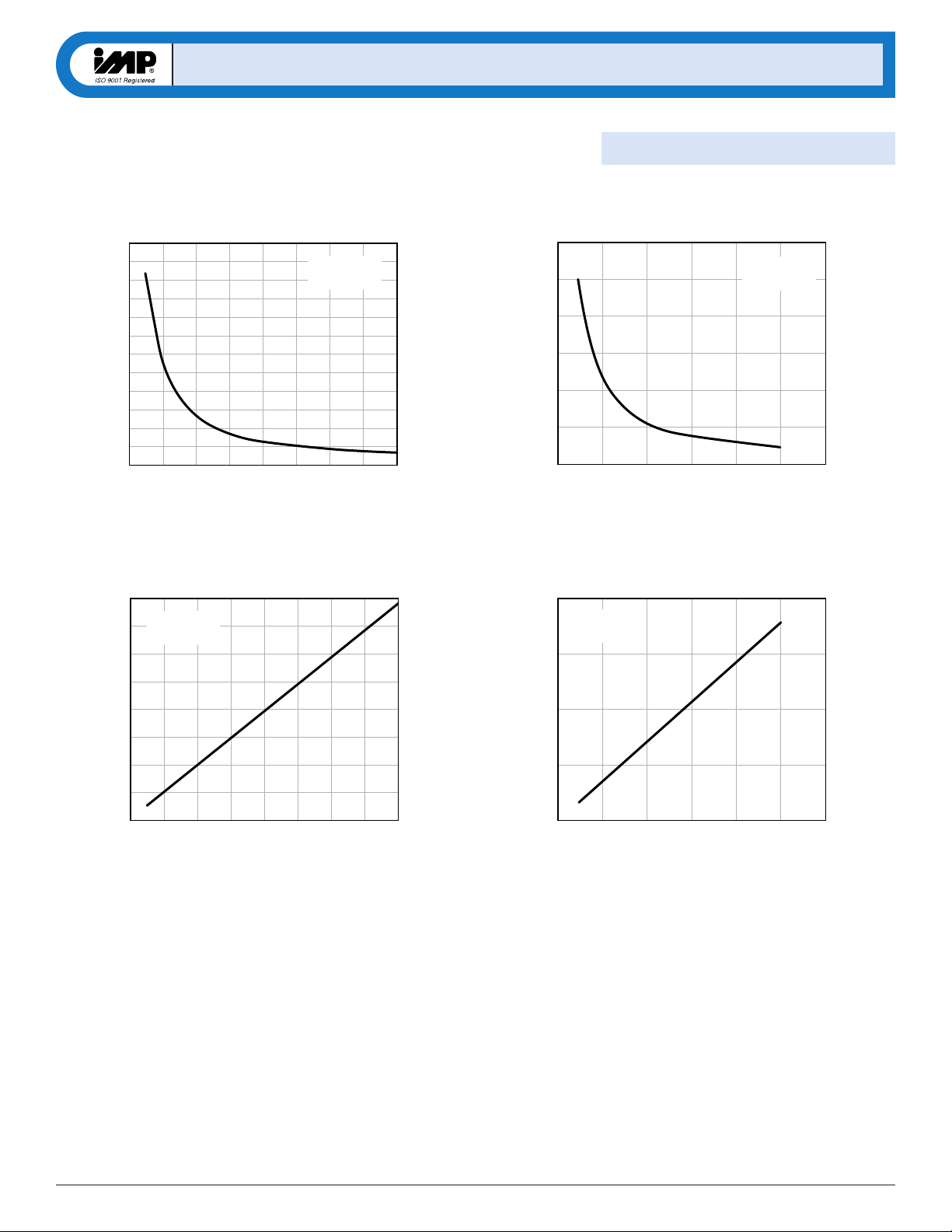
Typical Characteristics
Frequency (Hz)
REL (MΩ)
EL Lamp Drive Frequency
525_08.eps
VDD= 1.5V
TA= 25°C
0 0.5 1.0 1.5 2.0 2.5 3.0 3.5 4.0
0
400
800
1200
1600
2000
2400
Frequency (kHz)
RSW (MΩ)
525_10.eps
0 0.5 1.0 1.5 2.0 2.5 3.0
0
25
50
75
100
125
150
Boost Converter
Switching Frequency
VDD= 1.5V
TA= 25°C
Period (ms)
REL (MΩ)
525_07.eps
0 0.5 1.0 1.5 2.0 2.5 3.0 3.5 4.0
0
1
2
3
4
5
6
7
8
EL Lamp Drive Period
VDD= 1.5V
TA= 25°C
Period (ms)
RSW (MΩ)
525_09.eps
0 0.5 1.0 1.5 2.0 2.5 3.0
0
25
50
75
100
Boost Converter
Switching Period
VDD= 1.5V
TA= 25°C
 Loading...