

IMP IMP5111, IMP5112 User Manual
查询IMP5111供应商
I M P 5111/5112
®
ISO 9001 Registered
DESCRIPTION KEY FEATURES
The IMP5111/5112 SCSI terminators are part of
IMP's SCSI terminator family of high-performance,
adaptive, non-linear mode SCSI products, which are
designed to deliver true UltraSCSI performance in
SCSI applications. The low voltage BiCMOS
architecture employed in their design offers
performance superior to older linear passive and
active techniques. IMP's SCSI terminator
architecture employs high-speed adaptive elements
for each channel, thereby providing the fastest
response possible — typically 35MHz, which is 100
times faster than the older linear regulator/
terminator approach used by other manufacturers.
Products using this older linear regulator approach
have bandwidths which are dominated by the
output capacitor and which are limited to 500KHz
(see further discussion in the Functional Description
section). This new architecture also eliminates the
output compensation capacitor required in earlier
terminator designs. Each is approved for use with
SCSI-1, -2, -3, UltraSCSI and beyond — providing
the highest performance alternative available today.
Another key improvement offered by the
IMP5111/5112 lies in their ability to insure reliable,
error-free communications even in systems which do
not adhere to recommended SCSI hardware design
guidelines, such as the use of improper cable lengths
and impedances. Frequently, this situation is not
controlled by the peripheral or host designer and,
when problems occur, they are the first to be made
aware of the problem. The IMP5111/5112
architecture is much more tolerant of marginal
system integrations.
Recognizing the needs of portable and
configurable peripherals, the IMP5111/5112 have a
TTL compatible sleep/disable mode. Quiescent
current is typically less than 275µA in this mode,
while the output capacitance is also less than 3pF.
The obvious advantage of extended battery life for
portable systems is inherent in the product's sleepmode feature. Additionally, the disable function
permits factory-floor or production-line
configurability, reducing inventory and product-line
diversity costs. Field configurability can also be
accomplished without physically removing
components which, often times results in field
returns due to mishandling.
Reduced component count is also inherent in
the IMP5111/5112's architecture. Traditional
termination techniques require large stabilization
and transient protection capacitors of up to 20µF
in value and size. The IMP5111/5112 architecture
does not require these components, allowing all the
cost savings associated with inventory, board space,
assembly, reliability, and component costs.
9-Line SCSI Terminator
–35MHz Channel Bandwidth
■ ULTRA-FAST RESPONSE FOR FAST-20
SCSI APPLICATIONS
■ 35MHz CHANNEL BANDWIDTH
■ 3.3V OPERATION
■ LESS THAN 3pF OUTPUT CAPACITANCE
■ SLEEP-MODE CURRENT LESS THAN
275µA
■ THERMALLY SELF LIMITING
■ NO EXTERNAL COMPENSATION
CAPACITORS
■ IMPLEMENTS 8-BIT OR 16-BIT (WIDE)
APPLICATIONS
■ COMPATIBLE WITH ACTIVE NEGATION
DRIVERS (60mA / CHANNEL)
■ COMPATIBLE WITH PASSIVE AND
ACTIVE TERMINATIONS
■ APPROVED FOR USE WITH SCSI 1, 2, 3
AND ULTRA SCSI
■ HOT SWAP COMPATIBLE
■ PIN-FOR-PIN COMPATIBLE WITH
LX5211 AND UC5606 (IMP5111)
■ PIN-FOR-PIN COMPATIBLE WITH
LX5212 AND UC5603/5613/5614
(IMP5112)
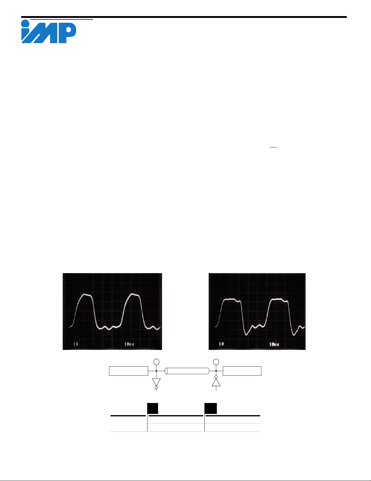
PRODUCT HIGHLIGHT
DRIVING WAVEFORM - 20MHZRECEIVING WAVEFORM - 20MHZ
Receiver
1 Meter, AWG 28
IMP
5111/5112
LX5268 LX5268
PACKAGE ORDER INFORMATION
T
(°C)
A
0 to 125
Note: All surface-mount packages are available in Tape & Reel.
Append the letter "T" to part number. (i.e. IMP5111CDPT)
Plastic SOIC
DP
16-pin, Power
IMP5111CDP IMP5111CPWP
IMP5112CDP IMP5112CPWP
Driver
Plastic TSSOP
PWP
24-pin, Power
IMP
5111/5112
1

ABSOLUTE MAXIMUM RATINGS (Note 1)
PACKAGE PIN OUTS
TermPwr Voltage ................................................................................................. +7V
Signal Line Voltage .................................................................................... 0V to +7V
Regulator Output Current ................................................................................... 0.4A
Operating Junction Temperature
Plastic (DP, PWP Packages) ......................................................................... 150°C
Storage Temperature Range .............................................................. -65°C to 150°C
Lead Temperature (Soldering, 10 seconds) ..................................................... 300°C
Note 1. Exceeding these ratings could cause damage to the device. All voltages are with
respect to Ground. Currents are positive into, negative out of the specified
terminal.
THERMAL DATA
DP¡ PACKAGE:
THERMAL RESISTANCE-JUNCTION TO LEADS, Q
THERMAL RESISTANCE-JUNCTION TO AMBIENT, Q
PWP PACKAGE:
THERMAL RESISTANCE-JUNCTION TO LEADS, Q
THERMAL RESISTANCE-JUNCTION TO AMBIENT, Q
Junction Temperature Calculation: TJ = TA + (P
The θ
numbers are guidelines for the thermal performance of the device/pc-board system.
JA
All of the above assume no ambient airflow.
D
x θ
).
JA
...............................................
JL
..................... 50°C/W
JA
..............................................
JL
.................. 100°C/W
JA
20°C/W
27°C/W
HEATSINK/GND
DISCONNECT *
T7
T8
T9
N.C.
GND
HEATSINK/GND
HEATSINK/GND
HEATSINK/GND
HEATSINK/GND
DISCONNECT *
T1
T2
GND
T7
T8
T9
T1
T2
1 16
215
314
413
512
611
710
89
T6
T5
N.C.
HEATSINK/GND
HEATSINK/GND
V
TERM
T4
T3
DP PACKAGE
(Top View)
1 24
223
322
421
520
619
718
817
916
10 15
11 14
12 13
PWP PACKAGE
(Top View)
*DISCONNECT for the IMP5112,
and DISCONNECT for the IMP5111.
T6
T5
N.C.
N.C.
HEATSINK/GND
HEATSINK/GND
HEATSINK/GND
HEATSINK/GND
N.C.
V
TERM
T4
T3
RECOMMENDED OPERATING CONDITIONS (Note 2)
Parameter
Termination Voltage V
High Level Enable Input Voltage IMP5111 V
IMP5112
Low Level Disable Input Voltage IMP5111 V
IMP5112
Operating Virtual Junction Temperature Range
IMP5111C/5112C
Note 2. Range over which the device is functional.
Symbol
TERM
IH
IL
Recommended Operating Conditions
Min. Typ. Max.
3.3 5.5 V
2V
0 0.8 V
0 0.8 V
2V
0 125 °C
TERM
TERM
ELECTRICAL CHARACTERISTICS
Term Power = 4.75V unless otherwise specified. Unless otherwise specified, these specifications apply at the recommended operating ambient temperature of
T
= 25°C. Low duty cycle pulse testing techniques are used which maintains junction and case temperatures equal to the ambient temperature.
A
Parameter
Symbol
Output High Voltage V
TermPwr Supply Current I
IMP5111 DISCONNECT Pin < 0.8V
IMP5112 DISCONNECT Pin > 2.0V
Output Current I
OUTVOUT
DISCONNECT Input Current IMP5111 I
DISCONNECT Input Current IMP5112 I
Output Leakage Current IMP5111 I
IMP5112 DISCONNECT Pin = > 2.0V, VO = 0.5V
Capacitance in DISCONNECT Mode C
Channel Bandwidth BW
Termination Sink Current, per Channel I
SINK
OUT
All data lines = open
CC
All data lines = 0.5V
= 0.5V
DISCONNECT Pin = 4.75V
IN
DISCONNECT Pin = 0V
DISCONNECT Pin = 0V
IN
DISCONNECT Pin = 4.75V
DISCONNECT Pin = < 0.8V, VO = 0.5V
OL
OUTVOUT
= 0V, frequency = 1MHz
V
= 4V
OUT
Test Conditions Units
LX5111/5112
Min. Typ. Max.
2.65 2.85 V
69mA
215 225 mA
275 µA
275 µA
-21 -23 -24 mA
10 nA
-90 µA
-90 µA
10 µA
10 nA
10 nA
3pF
35 MHz
60 mA
2
Units
V
V
 Loading...