


PRELIMINARY SF104-P01
SF3013M Fingerprint Image Sensor Module User Manual Page - 1
SF104x
Fingerprint Image Sensor Module
User Manual
February 7, 2014
Image Match Design Inc.
http://www.imagematch.com.tw/
B3-2, No. 1, Lising 1st Road, Hisnchu Science
Park, Hsinchu 300, Taiwan (R.O.C.)
Te l:+886-3-666-9388
Fax:+886-3-666-9387
Service:albertke@imagematch.com.tw

PRELIMINARY SF104-P01
SF3013M Fingerprint Image Sensor Module User Manual Page - 2
Revision History
Version Date Content Approved Checked Drawn
P01 2014/02/07 Initial draft Albert Ke
P02 2014/3012 I/O spec AL
P03 2014/03/17
Interface and drawing
update
Eros

PRELIMINARY SF104-P01
SF3013M Fingerprint Image Sensor Module User Manual Page - 3
Content
1 OVERVIEW .................................................................................................................... 5
1.1 DESCRIPTION ............................................................................................................ 5
1.2 FEATURES ................................................................................................................. 5
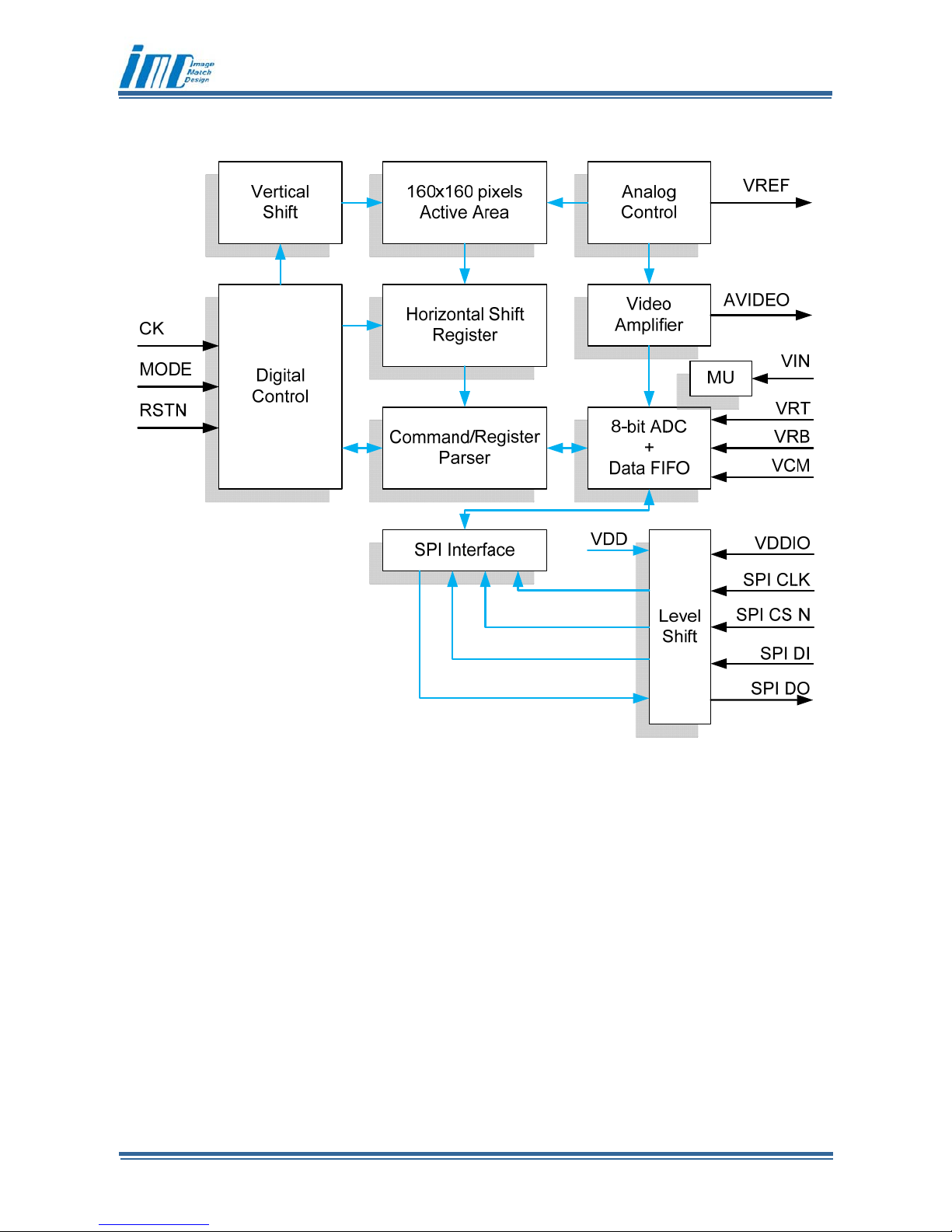
1.3 SENSOR BLOCK DIAGRAM .......................................................................................... 6
1.4 APPLICATIONS ........................................................................................................... 6
2 PHYSICAL DIMENSION ................................................................................................ 7
3 DEVICE OPERATION .................................................................................................... 7
3.1 SETTING UP CLOCK DIVIDER ........................................................................................ 7
3.2 CONFIGURING GAIN AND RANGE OF PRE-AMP AND ADC ................................................. 8
3.3 COMMAND AND REGISTERS ......................................................................................... 9
3.4 SPI COMMAND PROTOCOL ........................................................................................ 11
3.5 COMMAND CODE DETAIL ........................................................................................... 13
3.6 REGISTER DETAIL..................................................................................................... 15
4 OPERATION WORKFLOW ......................................................................................... 22
4.1 GENERAL DESCRIPTION ............................................................................................ 22
4.2 RESET .................................................................................................................... 23
4.3 FINGER DETECTION MODE AND INTERRUPT ................................................................. 23
4.4 TIMING CONSIDERATIONS .......................................................................................... 24
4.5 A SAMPLE SESSION .................................................................................................. 25
5 TIMING CHARACTERISTICS ...................................................................................... 28
5.1 SPI INTERFACE TIMING ............................................................................................. 28
6 MAXIMUM RATINGS AND OPERATING CONDITION ............................................... 31
7 ELECTRICAL CHARACTERIST I CS ............................................................................ 32
8 RELIABILITY TEST ..................................................................................................... 32
8.1 ESD IMMUNITY ........................................................................................................ 32
8.2 ENVIRONMENTAL LIMITS ........................................................................................... 33
8.3 MECHANICAL DURABILITY .......................................................................................... 33
9 PACKAGING INFORMATION ..................................................................................... 34
9.1 THE SF104X PACKAGING ......................................................................................... 34
9.2 SIGNAL DEFINITION................................................................................................... 34
9.3 PART DRAWING ........................................................................................................ 35
9.4 PIN CONFIGURATION ................................................................................................ 35

PRELIMINARY SF104-P01
SF3013M Fingerprint Image Sensor Module User Manual Page - 4
9.5 REFERENCE SCHEMATIC ........................................................................................... 36

PRELIMINARY SF104-P01
SF3013M Fingerprint Image Sensor Module User Manual Page - 5
1 Overview
1.1 Description
The SF104x fingerprint image sensor module is based on capacitive-contact
technology with hardened surface and enhanced ESD resistivity. The build-in analog and
digital circuitry minimizes the number of external component, and provides easy-to-use,
standard SPI interface to microprocessors.
The operation of SF104x is controlled through fingerprint image sensing by pixel array,
A/D converting, digital process, following is simple interface protocol. The captured image
quality of SF104x can be adjusted by setting gain, offset and reference voltage parameters.
In addition, the internal operation parameter and interface speed can also be configured to
the need.
1.2 Features
Spatial resolution 508 DPI
2D sensor array of 160x160 pixels
Active sensing area 8 mm x 8 mm
Build-in 8-bit ADC for digitizing image
Build-in programmable voltage reference
High speed SPI interface
0.03 sec read out time
128-byte on-chip data FIFO
PRELIMINARY SF104-P01
SF3013M Fingerprint Image Sensor Module User Manual Page - 6
1.3 Sensor Block Diagram
1.4 Applications
The compact, thin packaging of SF104x sensor module allows a wide range of
applications
Security devices
Fingerprint identification systems
Fingerprint recognition systems
PRELIMINARY
SF104-P01
SF3013M Fingerprint Image Sensor Module User Manual Page - 7
2 Physical Dimension
The sensor’s active pixel array is 160x160 pixels, and the SF104xM module is a
13.4mm*13.9mm highly integrated SPI fingerprint module.
3 Device operation
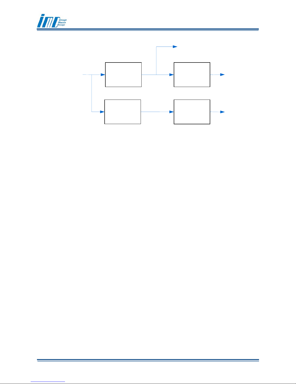
3.1 Setting up clock divider
The fingerprint sensor module has an on-board oscillator of 18Mhz, the sensor’s
internal clock logic is summarized as the following figure:
Sensor
& ADC
128-BYTE
FIFO
SPI
interface
Timing
Generator
Registers
Digital control
Register access
Analog control
D0~D7
D0~D7
ADCCLK
MCU
OTP
PRELIMINARY SF104-P01
SF3013M Fingerprint Image Sensor Module User Manual Page - 8
In the above diagram, OPCLK is used for internal timing, and PCLK is for image pixels.
The “detect start” signal starts the short “finger detect” cycle in detect mode.
The PCLK is 1/6 of OPCLK. OPCLK is the system clock pre-scaled by 1~16, controlled
by REG0/REG_CLK bit[3:0]. The detect start clock is controlled by REG9/REG_DDIV
bit[7:0].
For example, given the system clock input of 18Mhz, and REG0/REG_CLK bit[3:0]
value is 2 (divide by 3), then OPCLK is 6Mhz and PCLK is 1Mhz.
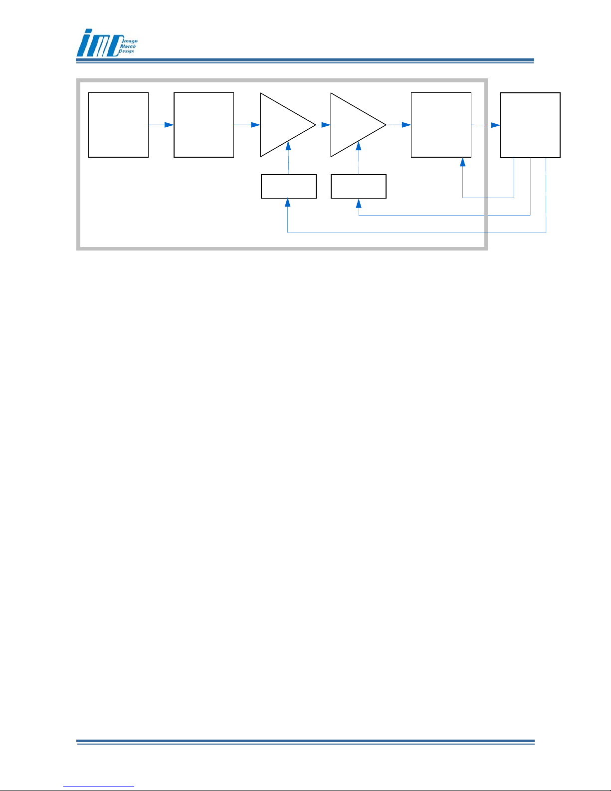
3.2 Configuring gain and range of pre-amp and ADC
Divide by
div_opclk
Clock from
external
oscillator
Divide
by 6
Divide by
4096
PCLK
OPCLK
Divide by
(DDIV+1)
detect
start
PRELIMINARY SF104-P01
SF3013M Fingerprint Image Sensor Module User Manual Page - 9
Two cascaded programmable gain amplifier are used for conditioning the sensor signal
before converted by ADC. Register REG1/REG_PGA bit [1:0] is for the control of PGA1 gain,
and register REG1/REG_PGA bit [7:4] for the control of PGA2 gain.
The ADC bias current and input voltage range is controlled by BIAS, (VRT-VRB) and
VRB parameters in REG3/REG_ADC. See section 5.0 for the detail of the registers.
3.3 Command and registers
The SF104 operation is controlled by sending commands and setting control registers
through the SPI interface. The SF104 SPI interface follows the SPI protocol with CPHA=0
and CPOL=0 as SPI mode 0.
There are 6 command codes to program the chip:
160x160
Pixel
array
Sample
&hold
ADC
MCU
Gain
Gain
VRT
VCM
VRB
PGA1 PGA2
PRELIMINARY SF104-P01
SF3013M Fingerprint Image Sensor Module User Manual Page - 10
command code name function read/write
0x01 rdata read pixel data R
0x02 start start scan W
0x03 status read status R
0xC0 srst software reset W
0x20+N rread read register R
0x40+N rwrite write register W
For the rread and rwrite command, the number N is the register address. The effective
N is in the range of 0x00 to 0x11.
The register content is summarized in the following table:
N Address Name Function RW
Default
Value
76543210
0 0x00 reg_clk clock control RW 0
1 0x 01 reg_pag pag control RW 0 en_test1 en_t est0
2 0x 02 reg_dcoc dc offs et RW 0
3 0x 03 reg_adc adc setting RW 0
4 0x 04 reg_otp_addr OTP address RW 0
5 0x 05 reg_otp_wdat OTP wirte dat a RW 0 otp_wd
6 0x 06 reg_otp_m ode OTP cont rol RW 0 otp_prg otp_rst otp_c eb
7 0x 07 reg_otp_rdat OTP read data RW
8 0x 08 reg_deth finger detection threshold RW 0xFF
9 0x 09 reg_ddiv cloc k divider for detect ion RW 0
10 0x0A reg_enab function enable bits RW 0 en_window en_inscan en_det en_sqwv lowcap en_osc en_analog
11 0x0B reg_mode mode cont rol bits RW 0 en_intr
12 0x0C reg_llx windowing function sett ing RW 0
13 0x0D reg_lly windowing function sett ing RW 0
14 0x0E reg_urx windowing funct ion setting RW 0x9F
15 0x0F reg_ury windowing funct ion sett ing RW 0x9F
16 0x10 reg_c hmd c hange mode W (N/A) ch_mode
17 0x11 reg_inscanline in s can detec tion line number RW 0x40
Reserve
Internal test
otp_rdat
test1 tes t0 div_opclk
pga2_gain pga1_gain
dc_offset
adc_bias adc_vrt adc_vrb
otp_yp
otp_ain
ury
in_sc an_line
deth
ddiv
en_bits
llx
lly
urx

PRELIMINARY SF104-P01
SF3013M Fingerprint Image Sensor Module User Manual Page - 11
3.4 SPI command protocol
Command and data are exchanged throught the SPI MISO and MOSI wires. Each byte
of data sent through the MOSI port brings back a received byte through the MISO port.
Commands can be cascaded one by another. The term “SPI command sequence” in
the following context is defined as a sequence of command code and data bytes exchange
within one active SPISEL strobe.
An SF104 command code may or may not have associated data. The “start” and “srst”
commands don’t have associated data, and take effect immediately after the command code
is sent.
For read/write data commands, the second byte will be the beginning of data byte or
bytes, as illustrated below:
read command
write command
Writing and reading a series of register content may look different. For writing to
consecutive registers, an internal address counter is incremented automatically after each
byte written. This design eliminates the need to repeat sending the 0x40+N command for
each byte. So the sequence of read/write commands may look like the following.

PRELIMINARY SF104-P01
SF3013M Fingerprint Image Sensor Module User Manual Page - 12
read sequence (the last command byte is a dummy command)
write sequence
read image sequence
In fact, except for the write register command (which writes a sequence of register
content), commands can be mixed in a single sequence like following:
mixed mode of read image and status sequence

PRELIMINARY SF104-P01
SF3013M Fingerprint Image Sensor Module User Manual Page - 13
3.5 Command code detail
Code 01 / RDATA command (read only)
This command pumps image data from FIFO and sends it to host
Code 02 / START command (write only)
This command starts fingerprint image scan
Code 03 / status read command (read only)
This command sends the 8-bit internal status flags to host.
The status flags are defined as below
Bit Function
0 Data FIFO is “half full”
1 Data FIFO is empty
2 Data FIFO is “almost full”
3 Data FIFO is full
4 Image scan active
5 Detect interrupt flag
6 Detect result is OK
7 (not used)

PRELIMINARY SF104-P01
SF3013M Fingerprint Image Sensor Module User Manual Page - 14
Code 0xC0 / SRST command (write only)
This command generates a software reset to the system. Its effect is the same as
hardware reset except that the register content is left unchanged.
Code 0x2N / register read command
This command starts reading register at address N
At least to bytes needs to be written, the first byte is the command code, and the second
(dummy) byte is for the register content.
Subsequent register read command can be cascaded in one command sequence.
Code 0x4N / register write command
This command starts writing registers starting at address N
The first byte is the command code, followed by subsequent bytes that are written to
registers starting at the specified starting address N.
Code 0x3E, 0x3F / Chip ID read command
These two command read back the chip id of high and low byte
0x3E : Chip ID High Byte – Value 0x01 for SF104.
0x3F : Chip ID Low Byte – Value 0x04 for SF104.
All command code as the first byte in a command sequence returns the state byte
(which can be explicitly read by the 03 command).

PRELIMINARY SF104-P01
SF3013M Fingerprint Image Sensor Module User Manual Page - 15
3.6 Register detail
REGISTER
NAME
ADD
R
R/W Bit(s) DEFAULT DESCRIPTION
REG_CLK 0 R/W
0000_0000 Clock control
[7:6]
Test mode 1
00 : AREGC[2]
01 : TESTPIN = VREF
10 : TESTPIN = VINPTST
11 : AREGC[0]
[5:4]
Test mode 0
00 : AREGC[3]
01 : TESTPIN = VAMP
10 : TESTPIN = CDS
11 : invert ADC data, TESTPIN = VGND
[3:0]
DIV_OPCLK
The 4-bit DIV_OPCLK value (0~15) is the divider defining the ratio between
system clock (OSC) and opclk:
opclk_freq = sysclk_freq / (DIV_OPCLK + 1)
REG_PGA 1 R/W
0100_0000 PGA Gain Control
[7:4] PGA2_GAIN

PRELIMINARY SF104-P01
SF3013M Fingerprint Image Sensor Module User Manual Page - 16
For the gain control of PGA2
PGA2 gain =PGA_gain*[(Vinp_pga-Vinn_pga)+Voff]/[2*(VRT-VRB)]*255
[3]
EN_TEST1
0 : Disable Test mode 1
1 : Enable Test mode 1
[2]
EN_TEST0
0 : Disable Test mode 0
1 : Enable Test mode 0
[1:0]
PGA1_GAIN
00 : 4.6
01 : 7.6
10 : 12.8
11 : 22.7
REG_DCOC 2 R/W
0000_0000 DC_OFFSET - DC offset control of PGA2
[7]
Sign bit
0 : negative
1 : positive
[6:0]
Offset compensated voltage
The DC offset voltage is set as the following formula:
Voff=0.4545*(2*B7-1)*[<B6:B0>/128*(VRT-VRB)+Vos1]
Vos1 ~ N(μ1,σ1) normal distribution, μ1=0 & σ1~=3.5mV~5mV
REG_ADC 3 R/W
0010_0101 Adc setting
[7] Not used
[6:4] ADC_BIAS

PRELIMINARY SF104-P01
SF3013M Fingerprint Image Sensor Module User Manual Page - 17
ADC bias current settings
000 : 8uA
001 : 12uA
010 : 16uA (default)
011 : 20uA
1xx : 24uA
[3:2]
ADC_VRT
(VRT-VRB) settings:
00 : 0.90V
01 : 1.05V (default)
10 : 1.20V
11 : 1.35V
[1:0]
ADC_VRB
VRB settings:
00 : 0.800V
01 : 0.844V (default)
10 : 0.933V
11 : 0.978V
REG_OTP_A
DDR
4 RW
0000_0000 OTP address
[7:5] Not used
[4:0]
OTP_YP
Byte address
REG_OTP_
WDAT
5 RW
0000_0000 OTP write data
[7:4] Not used
[3:1] OTP_AIN

PRELIMINARY SF104-P01
SF3013M Fingerprint Image Sensor Module User Manual Page - 18
Bit address for writing
[0]
OTP_WD
Write data
REG_OTP_
MODE
6 RW
0000_0000 OTP control
[7:3] Not used
[2]
OTP_PRG
OTP “PRG” control bit (Program enable)
[1]
OTP_RST
OTP “RST” control bit (Reset)
[0]
OTP_CEB
OTP “CEB” control bit (Enable, active low)
REG_OTP_R
DAT
7 R
OTP read data
[7:0]
OTP_RDAT
OTP read data
REG_DETH 8 RW
1111_1111 D et ec ti on th re shol d
[7:0]
DETH
Finger detection threshold value
See the “finger detection” section below
REG_DDIV 9 RW
0000_0000 Clock divider for detection interval
[7:0]
DDIV
A clock divider for finger detection interval
See the “finger detection” section below
REG_ENAB A RW 0000_0000 Enable bits

PRELIMINARY SF104-P01
SF3013M Fingerprint Image Sensor Module User Manual Page - 19
[7]
EN_WINDOW
Enable windowing mode
The windowing size is assigned by reg_llx, reg_lly, reg_urx and reg_ury
(0x0C~0x0F)
0 : Disable
1 : Enabl
[6]
EN_INSCAN_DET
Enable the in scan line detection mode
The finger detection scan line can be changed according to value of
reg_inscanline (0x11) if enable
0 : Disable
1 : Enable
[5]
EN_DET
Enable the detect mode
0 : Disable
1 : Enable
[4] Reserve
[3]
LOWCAP
Enable the low capacitance mode for the sensor array
0 : High capacitor (96ff), compensation capacitor (1.05 pF)
1 : Low capacitor (48ff), compensation capacitor (2.57 pF)
[2]
EN_OSC
Enable internal clock oscillator
0 : Disable
1 : Enable
[1] Not used

PRELIMINARY SF104-P01
SF3013M Fingerprint Image Sensor Module User Manual Page - 20
[0]
EN_ANALOG
Enable analog circuit
0 : Disable
1 : Enable
REG_MODE B RW
0000_0000 Mode control bits
[7] Not used
[6]
EN_INTR
Enable detect interrupt
0 : Disable
1 : Enable
[5] Not used
[4:0]
ENBITS
Must be set to value 21 (0x15H) to enable the chip
REG_LLX C RW
0000_0000 Windowing function position setting
[7:0] LLX

PRELIMINARY SF104-P01
SF3013M Fingerprint Image Sensor Module User Manual Page - 21
Windowing is a flexible function which user can read the image data within
160x160 pixel size according to your need.
The windowing size is assigned by 4 registers, REG_LLX, REG_LLY,
REG_URX and REG_URY.
Refer to following picture to how to set the windowing position and size.
REG_LLY D RW
0000_0000 Windowing function position setting
[7:0]
LLY
Refer to REG_LLX for details.
REG_URX E RW
1001_1111 Windowing function position setting
[7:0]
URX
Refer to REG_LLX for details.
REG_URY F RW
1001_1111 Windowing function position setting
[7:0]
URY
Refer to REG_LLX for details.
REG_CHMD 10 W
Change mode
[7:1] Not used
[0] CH_MODE

PRELIMINARY SF104-P01
SF3013M Fingerprint Image Sensor Module User Manual Page - 22
Change mode for switching mode.
See the “finger detection” section below.
REG_INSCA
NLINE
11 RW
0100_0000 Set in scan detection finger detection line number
[7:0]
INSCANLINE_NUMBER
In scan line number value which limitation is 0~0x9F or Y axis range when
enable windowing function.
4 Operation workflow
4.1 General description
The SF104 hardware design implements a protection scheme that fingerprint image
will only be delivered when “finger touch” is detected. If not, reading image will return invalid
data. After the finger first touch the sensor, it can detect the finger on sensor and continue
to read out fingerprint image to speed up the frame rate of image readout until finger remove
from sensor and it will output white image data after in scan line number. The process is
summarized in the diagram below:

PRELIMINARY SF104-P01
SF3013M Fingerprint Image Sensor Module User Manual Page - 23
4.2 Reset
There are 3 sources of Reset that can force the chip entering reset state (in which all
internal logic are disabled)
the hardware reset pin
the SPI software reset command
the reset caused by the content of REG_MODE (REG11) register, as described earlier.
However the internal SPI state machine can only be reset by the hardware reset pin.
Since the hardware reset pin is multiplexed with the interrupt signal, the hardware reset
pin becomes unavailable when the (finger detect) interrupt is enabled.
4.3 Finger detection mode and interrupt

PRELIMINARY SF104-P01
SF3013M Fingerprint Image Sensor Module User Manual Page - 24
The finger detection mode is enabled by setting the EN_DET bit (bit 5 of REG10) to 1.
Finger detect interrupt is enabled by setting the EN_INTR bit (bit 6 of REG11) to 1. Enabling
interrupt also changes the hardware Reset pin to INTR output pin.
In finger detection mode, the hardware logic will periodically scan the row which assign
by REG_INSCANLINE of the pixel array. In instead of sending pixel data to FIFO, the pixel
data bytes are summed up and compared with a threshold value (determined by the
REG_DETH/REG8) at the end of line. If the sum is greater than the content of REG8, then
the interrupt flag will be raised.
Once the “Detect result is OK” status bit or “finger detected” interrupt flag is raised, the
internal image channel will be opened to allow full image data to be transferred to MCU.
The timing period of detection scan is given by:
sysclk_freq / (4096 * (REG9+1))
If at the end of detect scan, the summed pixel is less than the threshold value, the
interrupt flag will be set to (or return to) 0, and also the image data channel will be closed.
Whenever the detection mode control bit is turned on or off, it is required to write (any
value) to the REG_CHMD (REG16) register to inform the internal logic to change the scan
geometry.
There are two status bits in the status register associated with detection mode:
Status.bit5 is the detection interrupt flag, which is set at the end of each detection scan,
and cleared whenever a new scan (either image scan or detection scan) is started.
Status.bit6 is the detection OK flag, which is only set or cleared at the end of a detection
scan. This bit is used to enable or disable the image channel.
Both bit5 and bit6 are cleared by reset.
4.4 Timing considerations

PRELIMINARY SF104-P01
SF3013M Fingerprint Image Sensor Module User Manual Page - 25
Several timing parameter should be kept in mind for good estimation of timing:
Upon power up, reset, or whenever detection mode is turned off, the delay time from
sending the start command to the first data byte available is about 180 pclk cycles.
For the subsequent scans, the delay time is reduced to 19 pclk cycles.
Image sample is taken at the speed of pclk, i.e., one pixel per pclk cycle.
There is a small delay of 11 pclk cycles between lines.
4.5 A sample session
The following sample procedure demonstrates a typical session.
function spiwrite(char *data, int cnt)
{
GPIO.SSEL = 0;
for (i=0; i< cnt; i++)
SPIWRITE(data[i]);
GPIO.SSEL = 1;
}
main ()
{
GPIO.RSTN=1;
GPIO.SSEL=1;
// make sure hardware reset is enabled
spiwrite({0x4A,0x00,0x00}, 3);
// hardware reset

PRELIMINARY SF104-P01
SF3013M Fingerprint Image Sensor Module User Manual Page - 26
GPIO.SRST=0;
GPIO.SRST=1;
// initialize registers
// detect threshold (REG8=128)
// detect divider (REG9=128)
// enable analog (REG10[0]=1)
# enable clock (REG10[2]=1)
# enable detect (REG10[5]=1)
# enable interrupt pin (REG11[6]=1)
spiwrite({0x40,0x32,0xE5,0x50,0x25,0x00,0x00,0x00,0x00,0x00,0x20,0x85,0x15,0x00,0x00,0x9F,0x9F},
17);
spiwrite({0x50,0x00},2); // inform chang of geometry
// software reset
spiwrite({0xc0},1);
// wait for interrupt
while (~GPIO.INTR)
nop;
// stop detect mode
spiwrite({0x4a,0x85},2);
spiwrite({0x4f,0x00},2); // inform change of geometry
again:
// start image scan
spiwrite({0x02},1);

PRELIMINARY SF104-P01
SF3013M Fingerprint Image Sensor Module User Manual Page - 27
// delay 180 pclk cycle or wait for FIFO status is half-full
GPIO.SSEL = 0;
SPISEND(0x03);
repeat {
byte=SPIREAD({0x03});
} until (byte.bit0 == 1);
GPIO.SSEL = 1;
// read image
GPIO.SSEL = 0;
SPISEND(0x01);
for (i=0; i<(160*160); i++)
image[i] = SPIREAD(0x01);
GPIO.SSEL = 1;
if (checkimage() != TRUE) {
adjust_setting();
goto again;
}
// waiting for the finger to be removed
// start detect mode
spiwrite({0x4a,0xa5},2);
spiwrite({0x4f,0x00},2); // inform change of geometry
GPIO.SSEL = 0;
SPISEND(0x03);
repeat {
byte=SPIREAD({0x03});

PRELIMINARY SF104-P01
SF3013M Fingerprint Image Sensor Module User Manual Page - 28
} until (byte.bit6 == 0); // wait until DETOK bit goes away
GPIO.SSEL = 1;
} // end of main
5 Timing characteristics
5.1 SPI interface timing
General SPI Timing
Instruction without return data
Instruction with return data

PRELIMINARY SF104-P01
SF3013M Fingerprint Image Sensor Module User Manual Page - 29
Terminating read by applying new command

PRELIMINARY SF104-P01
SF3013M Fingerprint Image Sensor Module User Manual Page - 30
SPI timing parameters
SYMBOL PARAMETER NOTE MIN. TYP. MAX. UNITS
f
CK
Clock frequency 1 18 MHz
t
RST
Reset time 1 50 ns
t
RD
Rise time for digital inputs 2 2 ns
t
FD
Fall time for digital inputs 2 2 ns
f
SPI_SCK
Frequency for SPI clock. 1 0
fCK
MHz
t
SCKL
Part of SPI_CK clock period,
during which SPI_CK is low.
1 23 ns
t
SCKH
Part of SPI_CK clock period,
during which SPI_CK is high.
1 23 ns
t
CSCKF
Time from falling edge on
SPI_CK to edge on SPI_CS_N
1 8 ns
t
CSCKR
Time from edge on SPI_CS_N to
rising edge on SPI_CK
1 8 ns
t
DSU
Setup time for data before rising
edge of SPI_CK
2 6 ns
t
DH
Hold time for data after rising
edge of SPI_CK
2 6 ns
t
SCKD
Delay from falling clock to data
available.
2 1 3 ns
t
SSU
Delay from SPI_CS_N low to
SPI_DI mode change.
2 1 3 ns
Note 1: Estimated value
Note 2: Simulated value

PRELIMINARY SF104-P01
SF3013M Fingerprint Image Sensor Module User Manual Page - 31
6 Maximum ratings and operating condition
6.1 Maximum rating
Symbol Parameter Conditions Value Unit
VDD Supply voltage -0.3 to 3.3 V
V
VDDIO
Supply voltage of I/O -0.3 to 3.3 V
VI1 Input pin voltage 1 (SPICLK,
SPIDI, SPICSn)
(Note1) -0.3 to V
VDDIO
+0.3 V
VI2 Input pin voltage 2 (RSTn) (Note2) -0.3 to V
VDDIO
+0.3 V
VO1 Output pin voltage 1( INTn,
SPIDO)
0.3V to V
VDDIO
+0.3V V
TA Operating temperature -20 70
℃
ST Storage temperature
-65
150
℃
PT10 Soldering temperature (10
seconds)
250
℃
PT
120
Soldering temperature (2
minutes)
183
℃
Note 1: Each Input and Output pin has internal ESD protection diode between pin and
VDDIO.
Note 2: V
I2
has internal pull high current of 100 µA.
6.2 Operating condition
Symbol Parameter Conditions Min. Typ Max Unit
VDD Supply voltage 2.6 3.0 3.6 V
VDDIO Supply voltage of I/O 1.65 1.8 3.6
IDD Total supply current (CLK =
4Mhz)
VDD=3.3 V 12 mA
IDDIO Total I/O supply current (CLK = VDDIO=3.3 1 mA

PRELIMINARY SF104-P01
SF3013M Fingerprint Image Sensor Module User Manual Page - 32
4Mhz) V
CLK System Clock 4 MHz
ESDKV ESD protection 15 kV
7 Electrical characteristics
Symbol Parameter Conditions MIN TYP MAX Unit
Digital inputs
VIH High level input voltage
0.8*VDD
V
VIL Low level input voltage
0.2*VDD
V
IIH High level input current 1 uA
IIL Low level input current 1 uA
CI Input capacitance
5
pF
Digital outputs
VoH High level output voltage
IOH = 1mA 0.8*VDD
V
VOL Low level output voltage
IOL = 1mA 0.2
0.5 V
8 Reliability Test
8.1 ESD immunity
The packaged sensor fulfills the following requirements with regard to ESD immunity:
PARAMETER REFERENCE CONDITIONS VA LU E UNITS
ESD IEC61000-4-2 Air discharge > ±15 KV

PRELIMINARY SF104-P01
SF3013M Fingerprint Image Sensor Module User Manual Page - 33
Table 9-1 Requirements for ESD immunity
The ESD immunity is achieved by the combination of a surface coating with ability to
withstand > ±6 kV, a drive frame and a primary drive electrode that leads charge away from
the sensor. The length of the internal wiring connecting the drive frame should be minimized
to increase the capacity to divert the fast ESD-pulses.
8.2 Environmental limits
The sensor chip fulfills the following requirements regarding to environmental
durability:
P ARAMETER REFERENCE CONDITIONS Normal Low Limit UNITS
Cold operational IEC60068-2-1 Ab 16h -20 0
℃
Hot operational IEC60068-2-2 Bb 16h +85 +55
℃
Cold storage IEC60068-2-1 AB 100h -40 -40
℃
Hot storage 100h +85
℃
Temperature cycling IEC60068-2-14 Na 30 min/30 min 200 cycles -40/+85 -40/+85
℃
Humid heat IEC60068-2-67 Cy 85ºC /85% RH 1000 1000 Hours
Table 9-2 Requirements for environmental performance
8.3 Mechanical durability
The sensor chip fulfills the following requirements with regard to mechanical durability:
P ARAMETER REFERENCE CONDITIONS REQUIREMENT
Abrasion Specified test method 1,000,000 cycles / 800g load Normal performance
Vibration IEC60068-2-64 Random Normal performance

PRELIMINARY
SF104-P01
SF3013M Fingerprint Image Sensor Module User Manual Page - 34
Table 9-3 Requirements for mechanical durability
9 Packaging information
9.1 The SF104 packaging
Size:13.4mm*13.9mm*1.1mm (with FPC)
9.2 Signal definition
Pin# Description
1 INTn
2 SPIDO (SPIMISO)
3 VDD
4 RSTn
5 SPICLK
6 GND
7 SPIDI (SPIMOSI)
8 SPICSn
9 ESD
10 VDDIO

PRELIMINARY SF104-P01
SF3013M Fingerprint Image Sensor Module User Manual Page - 35
9.3 Part drawing
9.4 Pin description
Pin Name Type Pin Description
INTn Output
An interrupt to the processor can be
generated by finger detection.
SPIDO
(SPIMISO)
Output Master In Slave Out
VDD Input
System power. Voltage supply for core
operation.
RSTn Input
A LOW on this pin resets the SF104x to take
on its default states
SPICLK Input
The SPI clock rate provided by the master
must not exceed 18MHz. depending on

PRELIMINARY SF104-P01
SF3013M Fingerprint Image Sensor Module User Manual Page - 36
Pin Name Type Pin Description
different application, SPICLK should be
adjusted for best image quality.
GND Power Ground
SPIDI
(SPIMOSI)
Input Master Out Slave In
SPICSn Input Chip select for SPI
ESD ESD Connect ESD pin to Ground for
VDDIO Input
System power. This voltage is supplied for IO
interface operation. Normally it can be tied to
the VDD if the IO operation voltage is 3.3V. If
lower IO voltage is needed, providing the right
IO voltage to this pin.
9.5 Reference schematic
VDD
GND
1M
chasis(ESDdrain)
MCU
SPIDI
SPIDO
SPICLK
SPICSN
RSTN
VDD
GND
ESD
SF104xM
TVS
10u
 Loading...