

Page 1

SERVICE MANUAL
NO. S1998E01
September 22, 1998
A901HT
Copyright
IIYAMA ELECTRIC CO., LTD.
710-1 Kitaowaribe, Nagano-shi 381-0014 JAPAN
Page 2

[ Revision Record ]
Rev. Section Contents
Page 3

CONTENTS
SAFETY PRECAUTION.............................................................................
1. SET-UP ADJUSTMENTS...............................................................................
Page
i-ii
1-15
2. TIMING CHART..............................................................................................
3. IC APPLICATION...........................................................................................
4. CIRCUIT DESCRIPTION.................................................................................
5. SERVICE PARTS LIST...................................................................................
6. EXPLODED VIEW.........................................................................................
7. DIAGRAMS...................................................................................................
16
17-19
20-27
28-53
54-61
62-64
NOTICE
The information in this document is subject to change without notice.
Page 4

1. SET-UP ADJUSTMENTS
The following adjustments should be made when a complete realignment is required or a new picture tube is
installed.
<Required measuring equipment>
Signal generator (Programmable video generator)........................ Leader 1604A
DC voltmeter (300V DC range)
Note: Digital multimeter can also be used.
High voltage probe (0-30kV DC)
Color analyzer.......................................................................... Minolta CA-100
Photometer............................................................................. Minolta LS-100
Electric field meter.................................................................... Combinova EFM 100
Scale (Two 50cm scales put together so that no visual aberration occurs.)
Frequency counter
Digital wattage meter
Landing meter........................................................................... LSS LND-070 or 072
Degausser
Interface adapter (Iiyama handmade)
Short-connector (Iiyama handmade)
<Preparation>
Place the monitor without tilting.
1.
Connect the signal cable from the signal generator to the monitor.
2.
Face the CRT screen to east so as not to be influenced by magnetic force.
3.
4.
Turn ON the Power Switch, and degauss the entire screen with degausser. è See "EXTERNAL DEGAUSS".
5.
Perform adjustment by setting the brightness to center and the contrast to maximum, except where
specifically indicated.
6.
Receive MODE 5 and turn ON the Power Switch. Perform adjustment after a warm-up of at least an
hour.
7.
Adjustment data is automatically saved in the memory when the on screen display disappears, when
another signal is received, or pressing the Menu and – Buttons at the same time.
Note: This monitor should be checked and adjusted by connecting it to a signal generator, then entering
and running the timing charts both below and of Chapter 2.
Comp
–
–
–
–
O
–
–
–
Sync
on
green
–
–
–
–
O
–
–
–
40.27
36.76
31.778
30.30
21.00
9.09
8.68
8.47
fH
(kHz)
24.8
27.3
31.5
33.0
47.6
110.0
115.0
118.0
The resolutions are only for your reference when using Leader 1604A.
*
Resolution*
640×400
608×420
640×400
712×419
1024×720
384×1152
400×666
400×1200
Sync polarity
H
V
N
N
N
N
N
P
N
N
N
N
P
P
P
P
P
P
Horizontal (µsec)
B
A
3.04
4.41
3.813
2.01
2.00
0.80
0.89
0.87
C
3.99
2.21
1.907
0.99
2.36
1.48
1.14
1.13
- 1 -
D
30.39
27.94
25.422
26.96
15.76
6.41
6.38
6.22
E
2.85
2.20
0.636
0.34
0.88
0.40
0.27
0.25
O
17.719
16.652
14.268
16.665
16.695
11.108
6.249
10.660
Vertical (msec)
P
0.322
0.074
0.064
0.061
0.084
0.027
0.026
0.025
Q
1.007
0.771
1.112
3.636
0.420
0.582
0.416
0.455
R
16.108
15.439
12.711
12.696
15.115
10.472
5.781
10.171
S
0.282
0.368
0.381
0.272
1.076
0.027
0.026
0.009
Page 5

ADJUSTMENT MODE
ADJ.MODE
E2PROM
S1
PWB-RS
Short-connector
There are two different modes available to adjust the monitor as described below. The adjustment with ‘o’ in front
of the title are only available under User Mode. The adjustments with ‘n’ in front of the title are only available under
Factory Mode. You can perform the other adjustments by either User or Factory Mode. Please change the mode
as required.
USER MODE:
Turn ON the Power Switch and you are in the User Mode.
FACTORY MODE: There are two ways to enter the Factory Mode.
1. Turn OFF the Power Switch. Connect the Iiyama short-connector to the RS connector on the PWBMAIN and set S1 switch on the PWB-RS of the short-connector to ADJ.MODE side. Turn ON the Power
Switch and you are in the Factory Mode. The following menu appears on the screen when you press the
MENU Button. Turn OFF the Power Switch and remove the short-connector from the RS connector to exit.
RS connector
PWB-MAIN
CRT
CRT face
2. Turn ON and OFF the Power Switch while pressing the MENU Button. Turn ON the Power Switch again while
pressing the – Button and you are in the Factory Mode. The following menu appears on the screen when you
press the MENU Button. Turn OFF the Power Switch to exit.
DF DP
The menu items in the Factory Mode are as follows:
Contrast
Brightness
V-size
V-position
H-size
H-position
Pin-cushion
Trapezoid
Parallelogram
Side-pin-balance
Side-pin-corner
Cushion-side
DEGAUSS
Uniform-VCENT
Uniform-V-TB
Uniform-HCENT
Uniform-H-RL
Landing-TL
Landing-TR
Landing-BL
Landing-BR
N-S RRC
DBF-Para
DBF-Phase
H-moire
H-convergence
V-convergence
Tilt-dy
V-linear-S
V-linear-C
Auto-da-test1
Auto-da-test2
Auto-da-test3 *
CRT Check
* Auto-da-test3 helps you to perform H/V-BLANKING and H/V-CONVERGENCE confirmations in this
SET-UP ADJUSTMENTS. The following items are displayed automatically in turn.
1. H/V-convergence è 2. Tilt-dy è 3. N-S RRC è 4. Landing-TL/TR/BL/BR è 5. H/V-blanking
- 2 -
Page 6

EXTERNAL DEGAUSS
Make sure you disable the Landing-TL/TR/BL/BR and N-S RRC settings before performing the external degauss.
Follow the procedure below depending on the adjustment mode you are in.
PROCEDURE
USER MODE
o
1) Select Degauss and press the MENU Button so that the Landing-TL/TR/BL/BR and N-S RRC will be
disabled.
2) Degauss the entire screen with degausser while the Degauss is activated (approx. 6 seconds).
FACTORY MODE
n
1) Select CRT Check and press the MENU Button so that the Landing-TL/TR/BL/BR and N-S RRC will
be disabled.
2) Confirm that the OSD stays displayed on the screen.
Note: If the OSD disappears, restart from 1).
3) Degauss the entire screen with degausser.
4) Press the MENU Button twice to turn off the OSD.
LOCK OUT FACILITY
User adjustable items can be restricted to the following three lock out types by setting the lock out facility as
described below.
Lock out type
A
B
C
PROCEDURE
1.To make the lock out facility available
1) Minimize the contrast with the front buttons.
2) Turn OFF and ON the Power Switch.
3) When degaussing starts, press the MENU, – and + Buttons in turn so that the lock out facility is activated.
Lock out type is switched in alphabetical order when you repeat the button operation.
2. To cancel the lock out facility
1) Minimize the contrast with the front buttons.
2) Turn OFF and ON the Power Switch.
3) When degaussing starts, press the MENU, + and – Buttons at the same time. Then, press the MENU, –
and + Buttons in turn so that the lock out facility is canceled.
Note: This button operation should be performed while degaussing.
Menu * / Adjustment item available
Menu 1
Menu 1, 3, 5
Contrast, Brightness
* It shows the number of the standard menu page.
- 3 -
Page 7

1-1. 80V-ADJ adjustment [PWB-MAIN]
Receive a cross-hatch inverted signal of MODE 5 when applying the AC
1)
voltage of 110±10V.
Connect the DC voltmeter between CONNECTOR TP and GND (chassis).
2)
Adjust the voltage to DC 80±0.5V with VR930 (+B ADJ).
3)
1-2. ANODE VOLTAGE adjustment [PWB-MAIN]
WARNING !
VR501 (HV-ADJ) has been carefully factory-adjusted for each unit in order
to satisfy regulations regarding X-radiation.
Further adjustment on VR501 shall not be performed.
In case of adjustment, the adjusted position of VR501 must be fixed by a
soldering iron to prevent it from rotating.
1)
Receive a cross-hatch inverted signal of MODE 5.
2)
Turn OFF the Power Switch.
3)
Connect a high-voltage probe between CRT anode and GND (chassis).
4)
Turn ON the Power Switch.
5)
Adjust the high-voltage to 27.0±0.1kV with VR501 (HV-ADJ).
Voltage
VR930
Voltage
+B ADJ
6)
Confirm the variation of high-voltage is within ±0.2kV when receiving MODE
1 and MODE 6 respectively.
7)
Turn OFF the Power Switch and remove the high-voltage probe.
1-3. SCREEN VOLTAGE adjustment [PWB-MAIN]
1)
Receive a cross-hatch inverted signal of MODE 5.
2)
Turn ON the Power Switch.
3)
Connect a high-voltage probe between LEAD-CONNECTOR SC on the
PWB-MAIN / CONNECTOR SC on the PWB-VIDEO and GND (chassis).
4)
Adjust the screen voltage to 630±10V with SCREEN VR located lower of
T501 (FBT).
Note: SCREEN VR should not be turned after the adjustment above.
VR501
T501(FBT)
HV-ADJ
Voltage
E
R
E
C
S
N
- 4 -
Page 8

1-4. POWER FACTOR CIRCUIT confirmation [PWB-MAIN]
1)
Receive a cross-hatch inverted signal of MODE 5.
2)
Turn OFF the Power Switch.
3)
Connect the DC voltmeter between TP4 and TP0.
4)
Turn ON the Power Switch.
5)
Confirm that the voltage is DC 400±10V.
6)
Remove the DC voltmeter.
1-5. TEMPERATURE SENSOR confirmation
n
1)
Receive a cross-hatch inverted signal of MODE 5.
2)
Select CRT Check and press the MENU Button.
3)
Confirm that respective temperature of fan and monitor front displayed
on the screen is as follows: actual temperature ±5°C.
1-6. FREE-RUNNING adjustment
n
1)2)Receive a cross-hatch inverted signals of fH 27.3kHz and 115.0kHz
respectively.
CRT Check
····
|||||
30
Fan
····
···········
30
Monitor front
Confirm that FREE-RUNNING adjustment is automatically performed.
1-7. FH-LIMITER confirmation
n
1)
Receive a cross-hatch inverted signal of fH 24.8kHz.
2)
Confirm that the picture disappears. Also, make sure the horizontal
oscillation frequency is within the specified range: 55-70kHz.
3)
Receive fH 27.3kHz and confirm that the picture is synchronized.
4)
Receive fH 118.0kHz and confirm that the picture disappears. Also, make
sure the horizontal oscillation frequency is within the specified range above.
5)
Receive fH 115.0kHz and confirm that the picture is synchronized.
6)
Turn OFF the power of signal generator and confirm that the picture
disappears. Also make sure the horizontal oscillation frequency is within
the specified range above.
7)
Remove the frequency counter.
1-8. H-SIZE LIMIT adjustment
n
1)2)Receive a cross-hatch inverted signals of fH 33.0kHz and 110.0kHz
respectively.
Adjust the horizontal size (H-size) to make it full-scan.
- 5 -
Page 9

Picture
Picture
Raster rolling
Raster tearing
1-9. H-BLANKING confirmation
n
1)
Receive a cross-hatch inverted signal of MODE 5.
2)
Minimize the horizontal size (H-size) with the front buttons.
3)
Select Auto-da-test3 and press the MENU Button so that the automatic
confirmation program starts.
4)
Confirm that X of the right hand side figure is as follows: X </= 3.0mm.
5)
Adjust the horizontal size roughly with the front buttons.
1-10. V-BLANKING confirmation
n
1)
Receive a cross-hatch inverted signal of MODE 5.
2)
Adjust the vertical size and position (V-size and V-position) of the picture
roughly with the front buttons.
3)
Select Auto-da-test3 and press the MENU Button so that the automatic
confirmation program starts.
4)
Confirm that the back-raster is not rolling or tearing at the top.
5)
Confirm that no retrace line is over the picture.
Raster rolling
x
Picture
1-11. V-LIN adjustment
n
1)
Receive a cross-hatch inverted signal of MODE 5.
2)
Adjust the vertical size so that the size is 270±4mm.
3)
Adjust the vertical linear corner (V-linear-C), so that difference between A
and B of the right hand side figure is as follows: | A–B | </= 0.5mm
4)
Adjust the vertical linear side (V-linear-S), so that A, B and C are almost
equal.
1-12. H-CENT adjustment [PWB-MAIN]
n
1)
Receive a cross-hatch inverted signal of MODE 5.
2)
Adjust the horizontal size and position of the picture roughly with the front
buttons.
3)
Maximize the brightness so that the back-raster appears on the screen.
4)
Set S501 to the right, center or left so that A and B in the right hand side
figure are almost equal.
5)
Return the brightness to center indication.
S501
Right
Back-raster
A
Picture
Bezel
A
C
B
Left
B
n
1-13. TILT-DY adjustment
1)2)Receive a cross-hatch inverted signal of MODE 5.
Adjust the tilt deflection yoke (Tilt-dy) with the +/– Buttons so that X of the
right hand side figure is as follows: | X | </= 0.5mm.
X
- 6 -
Page 10

1-14. PICTURE SIZE, POSITION AND DISTORTION adjustment (Criteria)
n
1)
Receive a cross-hatch inverted signal of MODE 4.
2)
Adjust the picture size and position to the specified setting below.
H-size: 360±4mm
V-size: 270±4mm
3)
Correct the side distortion with the front buttons so that X of the right hand
H-position: | A–B |<4mm
V-position: | C–D |<4mm
side figure is as follows: | X | </= 0.5mm/30mm when selecting the most
remarkable distortion with the naked eye.
Pin-cushion
Trapezoid
Side-pin-balance
1-15. PICTURE SIZE, POSITION AND DISTORTION adjustment
n
1)
Receive a cross-hatch inverted signal of fH 31.5kHz.
2)
Adjust the picture size, position and distortion roughly with the front buttons
Parallelogram
Side-pin-corner
Cushion-side
to the reference settings below.
H-size: 360±10mm
V-size: 270±10mm
H-position: | A–B |<8mm
V-position: | C–D |<8mm
| X | </= 1.0mm/30mm when selecting the most remarkable
distortion with the naked eye.
A
30mm
C
Picture
D
X
Pin-cushion
Trapezoid
B
Bezel
Picture
Note: The picture should be within the bezel.
3)
Receive a cross-hatch inverted signal of all preset modes respectively.
4)
Adjust the picture size and position to the specified setting below.
H-size: 360±4mm
V-size: 270±4mm
5)
Correct the Pin-cushion and Trapezoid distortion with the front buttons so
that X of the right hand side figure is as follows: | X | </= 0.5 mm/30mm
when selecting the most remarkable distortion with the naked eye.
Note: No other adjustment items for distortion than the above should be
adjusted.
1-16. RESET confirmation
o
1)
Receive a cross-hatch inverted signal of MODE 5.
2)
Change the horizontal position (H-Position) roughly with the front buttons.
3)
Perform Reset.
4)
Confirm that the adjustment data above is reset to the factory setting.
H-position: | A–B |<4mm
V-position: | C–D |<4mm
Side-pin-balance
Parallelogram
Side-pin-corner
Cushion-side
- 7 -
Page 11

1-17. Automatic COLOR adjustments
n
WARNING:
Do not change the horizontal and vertical sync signal or the frequency
while the automatic COLOR adjustments are underway.
Color analyzer setting:
Luminance unit switch: cd/m
l
B.P.S. DIP switch: 9600 (1000)
l
Turn ON the color analyzer switch and press 0-CAL switch before use.
l
1)
Be sure to enter the Factory Mode by using the short-connector.
2)
Connect the interface adapter from RS-232C of the color analyzer to the
PWB-RS of the short-connector.
3)
Select BNC for the signal input and receive a white window signal of MODE 4.
4)
Turn OFF the R, G and B outputs on the signal generator.
5)
Apply a color analyzer probe to the center of the screen.
6)
Turn ON the Remote Switch of the color analyzer so that “G” will appear
on the screen to inform that automatic CUT-OFF adjustment starts.
7)
Turn ON the R, G and B outputs on the signal generator when “GBRIN”
appears on the screen so that the COLOR TEMPERATURE and
CONTRAST LIMIT adjustments start automatically.
cd/m²
2
Luminance unit switch
1
0
B. P. S. DIP switch
fL
<COLOR TEMPERATURE>
The X and Y specified readings of the color analyzer are as follows:
CT 1 (9300K)
X: 0.283±0.006
Y: 0.297±0.006
CT 2 (6500K)
X: 0.313±0.006
Y: 0.329±0.006
CT 3 (5000K)
X: 0.345±0.006
Y: 0.352±0.006
<CONTRAST>
The specified contrast range is 120±6cd/m2.
Note: “G” appears again on the screen to indicate the contrast is not
within the specified range above. In that case, repeat 4) to 7).
8)
“END” appears on the screen to inform that the adjustments are completed.
9)
Turn OFF the Remote Switch of the color analyzer.
Note: The adjustments above can be repeated by turning OFF and ON the
Power Switch.
1-18. GRAY SCALE confirmationn
1)2)Receive a 16-gradation gray scale signal of MODE 4.
Make sure the 15th gradation on the gray scale is barely visible when the
16th gradation (back raster) is not visible at all.
- 8 -
Page 12

n
1-19. BRIGHTNESS adjustment [PWB-MAIN]
1)
Receive an entire white raster signal of MODE 4.
2)
Apply a photometer to the screen center.
3)
Adjust VR502 (ABL-ADJ) so that photometer reads 105±5cd/m2.
1-20. SYNC SIGNAL INPUT confirmation
n
1)
Receive a cross-hatch inverted signal of fH 47.6kHz.
2)
Select composite and sync on green signal inputs respectively by the
signal generator.
3)
Confirm that the picture is displayed normally.
1-21. SIGNAL SELECT confirmation
1)
Receive a cross-hatch inverted signal of MODE 5.
2)
Switch the signal input to BNC and D-SUB respectively.
3)
Confirm that the picture is displayed normally.
Brightness
VR502
ABL-ADJ
1-22. POWER MANAGEMENT confirmation
o
1)
Turn OFF the Power Switch and connect a digital wattage meter.
2)
Turn ON the Power Switch.
3)
Receive a cross-hatch inverted signal of MODE 5.
4)
Turn OFF the R, G and B outputs on the signal generator.
5)
Disconnect the H/HV and V cables.
6)
Confirm that the input wattage is 5W or less and the Power Indicator turns
to orange.
7)
Connect the H/HV and V cables and confirm that the picture appears.
8)
Turn OFF the Power Switch and remove the digital wattage meter.
9)
Turn ON the Power Switch.
1-23. H-CONVERGENCE confirmation
n
1)
Receive a cross-hatch inverted signal of MODE 5.
2)
Select Auto-da-test3 and press the MENU Button so that the automatic
confirmation program starts.
3)
Confirm that the horizontal line is diverged.
- 9 -
Page 13

1-24. V-CONVERGENCE confirmation
n
1)
Receive a cross-hatch inverted signal of MODE 5.
2)
Select Auto-da-test3 and press the MENU Button so that the automatic
confirmation program starts.
3)
Confirm that the vertical line is diverged.
1-25. RASTER REGULATION (DYNAMIC) confirmation
n
1)
Receive an entire white signal of MODE 5.
2)
Set the input signal by the signal generator as follows:
V-DISP-TIME: 150 V-POSI-TIME: 450
3)
Maximize the brightness or set the signal level to 0.9Vp-p by the signal
generator.
4)
Confirm that <W of the right hand side figure is 1.0mm or less when
turning the luminance volume on the signal generator to the maximum
and “1” respectively.
5)
Return the brightness to center indication.
Back-raster
Picture
W
FOCUS-B
FOCUS-A
1-26. FOCUS [PWB-MAIN]
n
1)
Receive a green cross-hatch signal of MODE 5.
2)
Adjust FOCUS-A VR of T501 (FBT) to make the vertical lines sharpest at
points L, M and R as shown in Fig 1.
3)
Adjust FOCUS-B VR of the T501 to make the horizontal center line
sharpest at points L, M and R as shown in Fig. 1.
4)
If the focus at points T and M is as shown in Fig. 2, adjust VR503 (V-DBF)
to make the horizontal lines have the same thickness at points T, M and
B. And adjust the FOCUS-B VR again to make the horizontal lines sharpest
at points T, M and B. (VR503 should not be adjusted when focus at points
T and M is optimum.)
5)
If the focus at points L and M is as shown in Fig. 3 or vice versa, adjust
DBF-Para to make the horizontal center line have the same thickness at
points L, M and R. And adjust the FOCUS-B VR again to make the
horizontal center line sharpest at points L, M and R. (DBF-Para should
not be adjusted when focus at points L and M is optimum.)
6)
Repeat 2) to 5) until the focus is optimum.
7)
Confirm no focus variation on the entire screen.
8)
Check the focus with red and blue respectively.
9)
Receive a H-character signal and repeat 7).
10)
Repeat the FOCUS adjustments until the focus with red, green and blue
is optimum.
SCREEN
Focus
VR503
L
Fig.1
Fig.2
L
Thin
Thick
T501(FBT)
V-DBF
M
T Thin
M Thick
B Thin
M
Thick
R
R
- 10 -
Fig.3
Page 14

1-27. LUMINANCE DIFFERENCE adjustment
n
1)
Receive an entire white signal of MODE 5.
2)
Apply a photometer to C (center), T (top), B (bottom), L (left) and R (right)
in the right hand side figure.
3)
Confirm that the luminance difference between C and T, C and B, C and L,
C and R is within ±10cd/m2 respectively.
4)
If the luminance difference is not within the specified range above, perform
the following adjustments:
<Point T or B>
1. Adjust Uniform-VCENT first to increase the brightness of T and B.
T
L
C
B
R
2. Adjust Uniform-V-TB so that the luminance difference between C and
2
T or C and B is within ±10cd/m
.
<Point R or L>
1. Adjust Uniform-HCENT first to increase the brightness of point L and R.
2. Adjust Uniform-H-RL so that the luminance difference between C and
L or C and R is within ±10cd/m
2
.
1-28. LUMINANCE DIFFERENCE confirmation
1)
Receive an entire white signal of MODE 5.
2)
Apply a photometer to the two points where the luminance difference is
remarkable with the naked eye.
3)
Confirm that the luminance difference is 22.5cd/m2 or less.
TL
T
L
C
B
TR
R
BRBL
- 11 -
Page 15

1-29. TCO requirement
1-29-1. VLF adjustment [PWB-MAIN]
Note: The VLF adjustment requires the precise measuring conditions. Make
sure the adjustment is carried out in the following environment.
1.
All metal parts should be attached to the monitor.
2.
All the electrical equipment used for the adjustment including the
monitor should be grounded to the same outlet.
Set the monitor and the electric field meter with tilt of zero degree at
3.
a distance of 29.5±0.5cm so that the CRT face will be parallel to the
electric field meter.
No other monitors should be placed in the area with a radius of 1.5m
4.
behind the center of monitor, between the monitor and the electric
field meter and 1.0m behind the electric field meter.
Keep at least 20cm between the monitors.
5.
The VLF level of background should be 0.3V/m or less when the
6.
monitor power cable is disconnected.
Receive a H-character inverted signal of MODE 6.
1)
Adjust the contrast so that the brightness at screen center is 60±5cd/m2.
2)
Set the brightness to center indication.
3)
Turn VR5T2 (VLF-2) fully counterclockwise.
4)
Adjust VR5T1 (VLF-1) so that the electric field meter reads the VLF level
5)
0.95V/m or less.
Monitor
Electric field meter
Monitor
20cm
VLF level
VR5T1 VLF-1
VR5T2 VLF-2
1.5m
29.5+0.5cm
1.0m
In case that the VLF level is not within the specified range above, adjust
6)
VR5T2.
In case that the VLF level is still not within the specified range above, turn
7)
VR5T2 fully clockwise and adjust VR5T1.
In case that the VLF level is still not within the specified range above,
8)
adjust VR5T2.
- 12 -
Page 16

1-30. ITC (Integrated Tube Component) adjustments
n
The following ITC adjustments should be made only when a new picture tube is installed, or convergence is poor.
All set-up adjustments above-mentioned must be completed before any further ITC adjustment is attempted.
Receive an entire white raster signal and turn ON the Power Switch. Perform adjustment after a warm-up of at least
an hour.
Perform the following adjustments by setting H-convergence and V-convergence to center indication.
Notes: See Chapter 5 concerning parts list for the ITC adjustments.
* PURITY MAGNET should not be turned during the ITC adjustments.
< Top view > < Side view >
PURITY MAGNET*
4-POLE MAGNET
6-POLE MAGNET
LOCKING RING
BOW MAGNET
Y
Y
V
X
CRT face
HC
Y
H
Y
VS
V
DIFFERENTIAL
COIL
X
V
DEFLECTION
YOKE
SEPARATOR
1-30-1. LANDING correction
Landing meter setting:
Mode Select Switch: Monitor Normal
l
Note: Mode Select Switch should be set before turning on the power switch of the landing meter.
Volt: 2V
l
Time: 50ms
l
Gain: 7
l
Unit: % for LND-070, 0.8µm (1%=0.8µm) for LND-072
l
1)
Face the CRT screen to east and set it vertically.
Degauss the entire screen with degausser. è See "EXTERNAL DEGAUSS".
2)
3)
Select DEGAUSS and press the MENU Button.
Receive an entire green signal.
4)
Adjust the horizontal size to make it full-scan.
5)
Apply the landing meter to TL (top-left), TR (top-right), BL (bottom-left) and
6)
BR (bottom-right) in the right hand side figure.
Confirm that "H" reading of the landing meter is within ±20% at each point.
7)
Adjust N-S RRC with the front buttons so that the "H" reading difference
8)
between T (top) and B (bottom) in the right hand side figure is as follows:
| T-B | = ±3%.
TL
BL
T
B
20mm
TR
BR
20mm
Adjust Landing-TL, TR, BL and BR respectively with the front buttons so
9)
that "H" reading of the landing meter at each point is as follows:
TL: –8 to –2% TR/BL: 0 to +6% BR: –6 to 0%
- 13 -
Page 17

1-30-2. Yvs adjustment
Notes: 1. This adjustment should be performed only when the picture
distortion in the right hand side figure is permitted.
2. Be sure to perform the 1-30-6. YV adjustment after this
adjustment because the convergence adjusted by YV volume
is changed at the same time during this adjustment.
1)
Receive a cross-hatch inverted signal.
2)
Adjust the specified Yvs volume so that the picture distortion is corrected.
1-30-3. STATIC CONVERGENCE adjustment
Receive a red and blue cross-hatch signal.
1)
Adjust the 4-POLE MAGNET so that red and blue beams converge on the
2)
center cross lines.
Add green to the red and blue cross-hatch signal.
3)
Adjust the 6-POLE MAGNET so that red and blue beams converge with
4)
green beam on the center cross lines.
Repeat the adjustment until red, blue and green beams converge each
5)
other.
Fix the 4-POLE MAGNET and the 6-POLE MAGNET by turning the
6)
LOCKING RING.
Bezel
Picture
R
B
G
R,B
R,G,B
Picture
B
R,B
Picture
R
G
R,G,B
Mark the 4-POLE MAGNET and the 6-POLE MAGNET with paint marker
7)
(090Z029A01) so that adjusted position is understandable.
1-30-4. BOW MAGNET adjustment
1)
Receive a red and blue cross-hatch signal.
2)
Adjust the BOW MAGNET so as to straighten an arched horizontal line.
Note: Must be careful not to misconverge vertical lines by this adjustment.
3)
Perform the 1-30-3. STATIC CONVERGENCE adjustment so as to converge
the red and blue lines.
4)
Fix the BOW MAGNET with paint (090Z020A01).
1-30-5. DIFFERENTIAL COIL adjustment (XV adjustment)
1)2)Receive a red and blue cross-hatch signal.
Adjust the DIFFERENTIAL COIL so that the horizontal cross line converge
each other.
R
B
B
R
R
B
R,B
- 14 -
Page 18

R
B
R,B
B
R
1-30-6. YV adjustment
1)
Receive a red and blue cross-hatch signal.
2)
Adjust the specified YV volume so that red and blue beams converge
each other at the upper and lower edges of the horizontal line.
B
R
R
B
R,B
R,B
1-30-7. YH adjustment
1)
Receive a red and blue cross-hatch signal.
2)
Adjust the specified YH volumes so that vertical cross lines converge
each.
1-30-8. SCREEN-CORNER MISCONVERGENCE correction
Receive a red and blue cross-hatch signal.
1)
Affix a *ferrite sheet (890Z003A02/890Z003A03) between SEPARATOR
2)
and CRT corresponding to the partially misconverged areas.
Note: Must be careful not to affect distortion by this correction.
Fix the ferrite sheet with ACETATE-TAPE (890P306A10).
3)
10
Y HYHC
R
B
B
R
B
R
R
B
10
Ferrite
100
70
(890Z003A02)
(890Z003A03)
(in mm)
*Ferrite sheet
- 15 -
Page 19

P
Q
R
S
O
V-parameters
O: Total period
P: Sync.width
Q: Back porch
R: Active video
S: Front porch
Video
Sync
2. TIMING CHART
- 16 -
Mode
VESA Timing Name
640×480
1
640×480
2
800×600
3
1024×768
4
B
@ 60Hz
@ 85Hz
@ 85Hz
@ 85Hz
C
fH
(kHz)
31.469
43.269
53.674
68.677
D
A
fV
(Hz)
59.940
85.008
85.061
84.997
E
Sync polarity
H
V
Comp
N
N
N
N
P
P
P
P
H-parameters
A: Total period
B: Sync.width
C: Back porch
D: Active video
E: Front porch
Sync
on
green
–
–
–
–
31.778
–
23.111
–
18.631
–
14.561
–
Horizontal (µsec)
A
B
3.813
1.556
1.138
1.016
C
1.907
2.222
2.702
2.201
D
25.422
17.778
14.222
10.836
E
0.636
1.556
0.569
0.508
O
16.683
11.764
11.756
11.765
Vertical (msec)
P
0.064
0.069
0.056
0.044
1.048
0.578
0.503
0.524
Q
R
15.253
11.093
11.179
11.183
S
0.318
0.023
0.019
0.015
1280×1024
5
6
1600×1200
@ 85Hz
@ 85Hz
91.146
106.250
85.024
85.000
P
P
–
P
P
–
10.971
–
9.412
–
1.016
0.837
1.422
1.325
8.127
6.972
0.406
0.279
11.761
11.765
0.033
0.028
0.483
0.433
11.235
11.294
0.011
0.009
Page 20

3. IC APPLICATION
Ref No. Description
Deflection circuit
IC350 UPC1884CT
IC401 LA7840L Vertical output
IC502 SLA5041 FET array
IC503 324
IC205 7805 5V regulator
IC206 PQ6RD083
IC304 7805 5V regulator
IC351 7812 12V regulator
IC702 7812
IC709 7805 5V regulator
IC930 3842 Main power control
IC931 MIP0223SY Sub power control
IC932 MC34262/
MC33262
IC960
IC961
IC962
IC211 M62393P D/A converter
IC301 741Z610-10 Main microprocessor
IC302 M51951BSL Power voltage watcher
IC303 24C08 E2PROM
7812 12V regulator
3842 Variable B control
UPC1093J/
KIA431
H&V synchronous signal processor
with geometrical compensation, H&V
oscillator
Amplifier (H-size, Distortion
control)
Power circuit
6.3V regulator (to CRT heater voltage)
12V regulator
Power factor control
Over voltage, Arc and X-ray protect
control
Microprocessor circuit
Application
Ref No. Description
Sub microprocessor circuit
IC701
IC703
IC501
IC101 M52755SP
IC102
IC201
IC202
IC203
IC207
IC210
IC704
IC705
IC706 LA6510/
IC707
IC708
741Z611-10
M62393P D/A converter
High voltage circuit
MSPAD104
24LC21
M52742ASP Video amplifier
LM2403T Video output
M35045 On screen display control
M52759SP Uniformity control
324 Amplifier (Cut-off control)
LA6510/
TA8410AK
LA6510/
TA8410AK
TA8410AK
LA6510/
TA8410AK
TMC3000NF
Application
Sub microprocessor
High voltage control
Video circuit
Signal switch
DDC
CRT circuit
Power amplifier
(TILT+/–, NS+/–)
Power amplifier
(H-CONV+/–, V-CONV+/–)
Power amplifier
(TL+/–, BL+/–)
Power amplifier
(TR+/–, BR+/–)
Terrestrial magnetic sensor
Note: Specifications of Main microprocessor and Sub microprocessor are on next page.
- 17 -
Page 21

Main microprocessor specifications
Pin
1
2
3
4
5
6
7
8
9
10
11
12
13
14
15
16
17
18
19
20
21
22
23
24
25
26
27
28
29
30
31
32
Name
H-LIN2
H-LIN1
DRIVE
SW
S.O.G.
GND
N.C.
N.C.
N.C.
500KHz
84-SDA
84-SCL
GND
GND
GND
GND
Vss
+ KEY
GND
GND
GND
GND
GND
– KEY
MENU
GND
CLAMP
DEG
PS1
LED-O
LED-G
Vss
H-LIN2 switching signal output
H-LIN1 switching signal output
DRIVE switching signal output
BNC/D-SUB switching signal
S.O.G.
GND
N.C.
N.C.
N.C.
CLOCK signal output for 1884 counter
1884 DATA input/output terminal
1884 CLOCK terminal
GND
GND
GND
GND
GND
Front-key signal input terminal
GND
GND
GND
GND
GND
Front-key signal input terminal
Front-key signal input terminal
GND
CLAMP
Degauss control signal output
POWER-SAVE control signal output 1
LED control signal output (Orange)
LED control signal output (Green)
GND
Function
Pin
64
63
62
61
60
59
58
57
56
55
54
53
52
51
50
49
48
47
46
45
44
43
42
41
40
39
38
37
36
35
34
33
Name
Avref.
AVDD
EP-SDA
EP-SCL
CS6
CS5
CS4
CS3
CS2
CS1
GND
GND
GND
GND
X1
X2
VDD
RxD
TxD
DIAG
V-SYNC
RESET
GND
S.O.G.
D/A-SCL
OSD-CS
OSD-SCL
SUB-SCL
SUB-SDA
SUB-SDA
Pre-SCL
Pre-SDA
Function
5V Vcc
5V Vcc
E2PROM DATA terminal
2
E
PROM CLOCK terminal
Cushion-S switching signal 6
Cushion-S switching signal 5
Cushion-S switching signal 4
Cushion-S switching signal 3
Cushion-S switching signal 2
Cushion-S switching signal 1
GND
GND
GND
GND
X'TAL 8MHz
X'TAL 8MHz
5V Vcc
Automatic adjustment DATA output terminal
Automatic adjustment CLOCK terminal
Automatic adjustment DATA input terminal
IIC-BUS reference signal input terminal
Main microprocessor RESET signal input terminal
GND
S.O.G.
D/A CLOCK output terminal
OSD SELECT signal output terminal
OSD CLOCK input/output terminal
Sub E2PROM CLOCK terminal
Sub E2PROM DATA input terminal
Sub E2PROM DATA output terminal
Pre-Amp CLOCK output terminal
Pre/OSD/DA-DATA output terminal
- 18 -
Page 22

Sub microprocessor specifications
Pin
1
2
3
4
5
6
7
8
9
10
11
12
13
14
Name
DA-SDA
DA-SCL
N.C.
N.C.
GND
RESET
X0
X1
GND
N.C.
M-SDA
M-SDA
M-SCL
N.C.
Function
D/A DATA input/output terminal
D/A CLOCK output terminal
N.C.
N.C.
GND
Sub microprocessor RESET signal input
terminal
X'TAL 4MHz
X'TAL 4MHz
GND
N.C.
2
Main E
Main E2PROM DATA input terminal
Main E2PROM CLOCK terminal
N.C.
PROM DATA output terminal
Pin
28
27
26
25
24
23
22
21
20
19
18
17
16
15
Name
ON-TIME
Temp.
AD-Vref
5V
N.C.
N.C.
GND
GND
GND
X
Y
N.C.
N.C.
N.C.
Function
5V Vcc
N.C.
POWER-ON time detection
Temperature detection
N.C.
A/D reference voltage 5V
GND
GND
GND
Magnetism sensor detection
Magnetism sensor detection
N.C.
N.C.
N.C.
- 19 -
Page 23

4. CIRCUIT DESCRIPTION
4-1. POWER FACTOR circuit
Q The full-wave rectified voltage waveform from D942 and smoothed voltage waveform from C926 are multiplied and
compared to R the voltage waveform from current detect resistor R925 of Q934. Q934 is turned off when R
exceeds Q, and is turned on when R is 0V. The above repetition is to change input current to substantially
sinusoidal waveform and it corrects harmonic distortion. The switching frequency is not constant as Q934 is turned
on or off by monitoring input voltage and load current. Therefore, this circuit is not synchronized with the MAIN
POWER circuit.
Switching frequency is minimum when input voltage is low and load current is maximum, in other words, the
switching frequency is maximum when input voltage is high and load current is minimum. (Switching frequency is
approx. 20-250kHz)
This circuit is operated by the voltage supplied to IC932 from the SUB POWER circuit so that it is not activated at
power management state.
0V
AC
90-132/
198-264V
D942
T932
IC932
5
D943
7
Q934
To pin 1
of IC932
R925
POWER FACTOR circuit
C926
0V
R926
R927
R928
+400V
DC
0V
- 20 -
Page 24

4-2. MAIN POWER circuit
400V is supplied to this circuit from the POWER FACTOR circuit. This circuit is fly-back type circuit which includes
IC930 controls PWM (Pulse Width Modulation) CONTROL circuit. The T930 secondary provides the following DC
voltages:
Q 80V line: Supplied to the DBF (Dynamic Beam Focus), HIGH VOLTAGE OUTPUT CONTROL,
and the CUT-OFF CONTROL circuits and the VIDEO OUTPUT IC as power source.
R 28.5V line: Supplied to the HORIZONTAL DEFLECTION OUTPUT (Variable B voltage control) and the
HORIZONTAL DRIVE circuits as power source.
S 16V line: Supplied to the VERTICAL DEFLECTION OUTPUT circuit as power source.
Divided 16V line is regulated to 12V by IC960 and supplied to the HORIZONTAL DEFLECTION
OUTPUT and HIGH VOLTAGE OUTPUT CONTROL and VIDEO SIGNAL PROCESSING circuits,
regulated to 12V by IC351 and supplied to the CONTROL SYSTEM circuit, regulated to
12V by IC702 and supplied to the CRT CORRECTION circuit and TERRESTRIAL MAGNETIC
SENSOR (IC708), regulated to 5V by IC709 and supplied to SUB MICROPROCESSOR
(IC701), D/A CONVERTER (IC703) and TEMPERATURE SENSOR as power source.
T –12V line: Supplied to the VERTICAL DEFLECTION OUTPUT and the CRT CORRECTION circuits as
power source.
U B9 voltage: The 28.5V line is pressured up to B9 voltage by the PWM CONTROL circuit which includes
(35-155V) IC961 and Q962. The voltage from the D973 cathode is supplied to the HORIZONTAL
DEFLECTION OUTPUT and the HIGH VOLTAGE OUTPUT circuits as power source.
This circuit is controlled by the voltage supplied from the SUB POWER circuit and it is not activated at power
management state. Therefore, no secondary provides the DC voltages.
AC
90-132/
198-264V
D942
IC930
POWER FACTOR
circuit
6
Q930
R932
T930
2
3
1
28.5V
16V
80V
IC961
4
–12V
L961
6
D973
Q962
R966
5
IC702
IC709
IC960
IC351
B9 (35-155V)
12V
5V
12V
12V
16V
- 21 -
Page 25

4-3. SUB POWER circuit
IC931 included in this circuit consists of the POWER MOS-FET and the CONTROL circuits and modulates the
pulse width. The current fed back from pin 9 of T931 is input to the control terminal of IC931. The T931 primary
provides the DC voltage (approx. 20V) to the POWER FACTOR and the MAIN POWER circuits as power source.
The T931 secondary provides the DC voltage (approx. 8.5V). Divided 8.5V line is regulated to 5V by IC304 and
supplied to the MAIN MICROPROCESSOR (IC301), IC350, VIDEO SIGNAL SWITCHING (IC101), DDC (IC102)
and TEMPERATURE SENSOR, regulated to 6.3V by IC206 and supplied to the CRT heater voltage, also regulated
to 5V by IC205 and supplied to the VIDEO AMPLIFIER (IC201), OSD CONTROL (IC203) and D/A CONVERTER
(IC211) as power source. The voltage at pin 1 of IC931 is 5.7V generally. This circuit is not synchronized with MAIN
POWER circuit as the oscillation frequency is fixed to approx. 100kHz.
400V
5.7V
1
POWER FACTOR and
MAIN POWER circuits
To
IC931
20V
T931
3
D964
8.5V
IC304
IC206
IC205
5V
CRT heater
5V
4-4. PROTECTION circuit
To prevent damage to the monitor, X-ray radiation etc., the POWER FACTOR and the MAIN POWER circuits stop
in the following cases:
+16V line: The voltage exceeds 23V.
+8.5V line: The voltage exceeds 15V.
+400V line: The voltage exceeds 460V.
Variable B voltage line: The voltage exceeds 200V.
X-ray protection circuit: The voltage exceeds 30kV.
Arc limit circuit: The beam current exceeds 2.9mA.
4-5. DISPLAY POWER MANAGEMENT circuits
(1) Stand-by / Suspend state:
When receiving no video signal and no horizontal or vertical sync signal for 6 seconds, pin 29 of IC301 turns to
5V from 0V. PC930 is turned on to stop power supply to the POWER FACTOR and the MAIN POWER circuits.
The power consumption is 10W or less.
(2) Active-off state:
When receiving no video signal and no horizontal and vertical sync signals for 6 seconds, pin 29 of IC301 turns
to 5V from 0V. Also, pin 16 of IC301 turns to 5V from 0V so that IC204 is turned on. The output from IC206 stops
and the heater voltage is turned off. The power consumption is 6W or less.
4-6. DEGAUSS circuit
As K930 is turned on when the power on, the degauss current flows through degauss coil and PR930 to degauss
the CRT. After approx. 6 seconds from power on, K930 is turned off automatically. As for manual degauss by the
adjustment item of Degauss, the degauss is performed in the same way.
- 22 -
Page 26

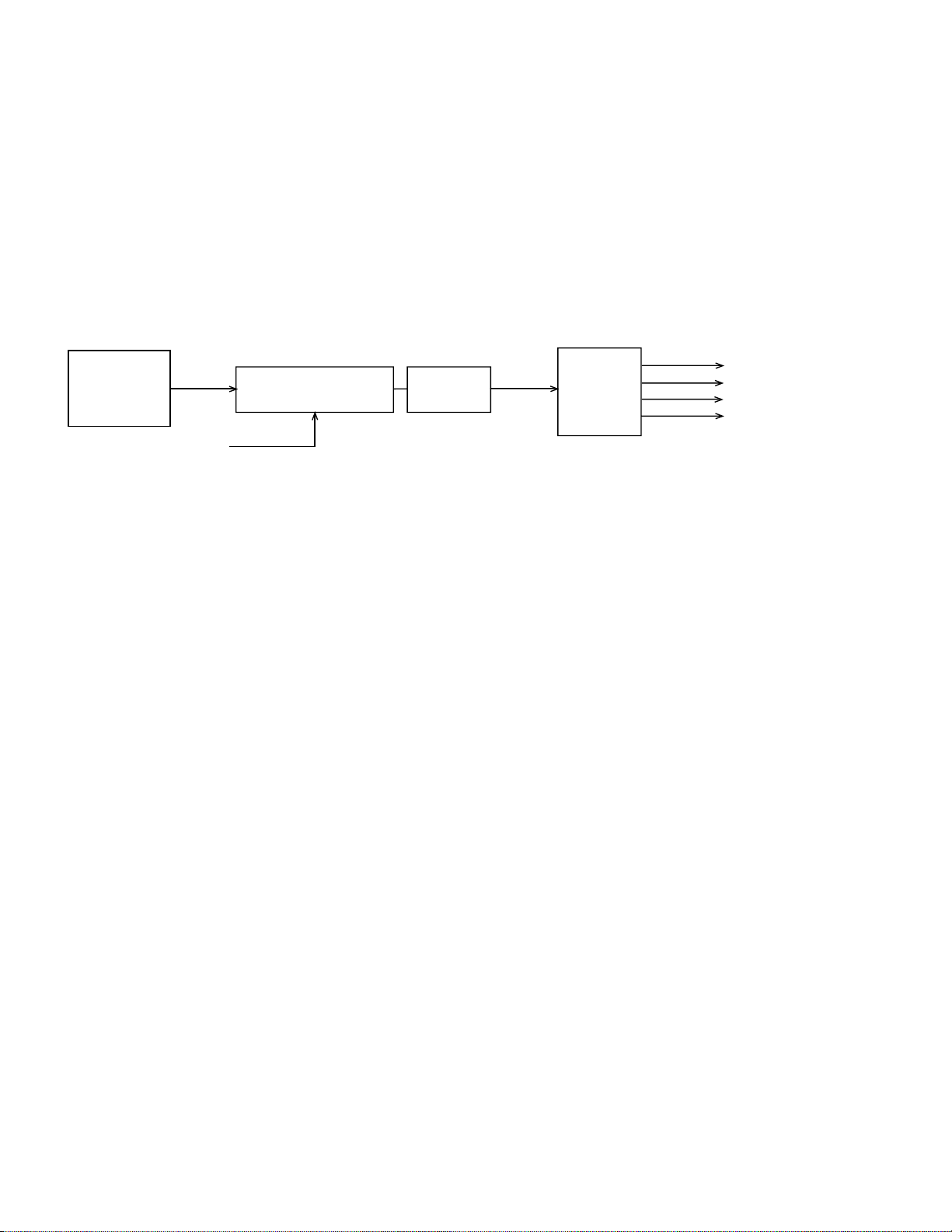
4-7. SIGNAL PROCESSING circuit
500kHz
Pin 29 of IC350
Input signal from D-SUB or BNC connector is converted to the waveform by IC101. The input signal is applied to pin
17 of IC101 from the MAIN MICROPROCESSOR (IC301) and then switched to D-SUB when pin 17 of IC101 is
“HIGH” level (5V), or to BNC when pin 17 of IC101 is “LOW” level (0V). When only one of the two signal inputs is
connected to the signal source, the one connected is automatically selected. When both of the signal inputs are
connected to the signal source, the latest one connected just before power off is selected. The adjustment item of
Signal Select also selects D-SUB or BNC. The selected input signal is converted to the waveform by IC101. The
sync signal is input to IC350 and the video signal is input to IC201.
4-8. SYNC SIGNAL PROCESSING circuit
The input sync signal to IC350 is processed inside IC350
as follows:
Q Detect the input sync signal presence
R Discriminate the input sync signal type: Separate /
Composite / Sync On Green
S Discriminate the sync polarity: Positive / Negative
T Count the frequency
500kHz clock signal supplied to pin 29 of IC350
counts the frequency. The frequency is sent to the
MAIN MICROPROCESSOR (IC301) to store Q-
T in the E2PROM as a read data.
H/V
INPUT
MAIN MICROPROCESSOR
SWITCHING
IC301
4-9. CONTROL SYSTEM circuits
4-9-1. H-SIZE and DISTORTION CORRECTION CONTROL
VIDEO
SIGNAL
IC101
IIC-BUS
H/V
H&V SYNCHRONOUS
SIGNAL PROCESSOR
H&V OSCILLATOR
IC350
The parabolic wave output from pin 9 of IC350 is adjusted and converted to the waveform by IC503 and then input to
pin 2 of IC961.
a (Approx. 8V): DC bias....H-size control
b (Approx. 1Vp-p): AC amplitude....Distortion control
b
a
0V
Pin 9 of IC350
The parabolic wave input to pin 2 of IC961 is added to the PWM waveform from pin 6 of IC961. The V-parabolic wave
modulates the variable B voltage to perform distortion correction.
c
c: H-size adjustment level
0V
Variable B voltage waveform
(D973 cathode)
- 23 -
Page 27

4-9-2. HORIZONTAL OSCILLATION
A drive pulse output from pin 17 of IC350 is amplified by Q350 and then applied to Q504 gate of the DRIVE circuit.
0.7V
0.2V
0V
Pin 17 of IC350 Inversion-amplified
waveform by Q350
12Vp-p
4-9-3. VERTICAL OSCILLATION
The sawtooth-wave is output from pin 8 of IC350 and applied to the VERTICAL DEFLECTION OUTPUT circuit.
a (Approx. 6.5V): AC amplitude....V-size control
b (Approx. 3.5V): DC bias....V-position control
a
Pin 8 of IC350
Reference voltage 5V
(Pin 23 of IC350)
b
4-10. HIGH VOLTAGE OUTPUT CONTROL circuit
The AFC waveform is output from pin 6 of L501 and applied to IC501. The duty-controlled voltage waveform is output
from pin 1 of IC501 and amplified by Q521 and then applied to T501. The applied voltage is amplified by T501 and
supplied to the CRT as anode voltage.
4-11. HORIZONTAL DEFLECTION OUTPUT circuit
The drive pulse is output from pin 17 of IC350 and amplified by Q350. The drive pulse is supplied to Q503 base via
HORIZONTAL DEFLECTION circuit and current-amplified.
4-12. VERTICAL DEFLECTION OUTPUT circuit
The sawtooth wave from pin 8 of IC350 is supplied to pin 5 of IC401 and amplified, and then supplied to the vertical
DY as sawtooth wave current. Vertical deflection is performed by the magnetic field generated when supplying the
current to the vertical DY.
+15V
Reference voltage 1.7V
Pin 2 of IC401
–10V
- 24 -
Page 28

4-13. DYNAMIC BEAM FOCUS circuit
The H-parabolic wave from pin 13 of IC350 is amplified by 18 times by Q518 and Q519 respectively. The amplified
parabolic wave is pressured up to 500vp-p by T503 and combined with V-parabolic wave and then added to pin 13
of T501.
5V
2V
0V
Pin 13 of IC350
V-parabolic wave from pin 12 of IC350 is amplified by Q520 and combined with H-parabolic wave.
5V
3V
0V
Pin 12 of IC350
4-14. SWITCHING SIGNAL circuit (CS SWITCHING POINTS)
Each switching point performs horizontal linear and distortion correction as follows:
IC301 output pin
CS6
DRIVE
H-LIN1
fH (kHz)
23.5 - 28.0
28.1 - 34.0
34.1 - 41.0
41.1 - 45.0
45.1 - 49.0
49.1 - 59.0
59.1 - 66.0
66.1 - 73.0
73.1 - 84.0
84.1 - 88.5
88.6 - 97.0
97.1 - 115.0
CS1
(Pin 55)
LOW
LOW
HIGH
HIGH
HIGH
HIGH
HIGH
HIGH
HIGH
HIGH
HIGH
HIGH
CS2
(Pin 56)
LOW
HIGH
LOW
LOW
HIGH
HIGH
HIGH
HIGH
HIGH
HIGH
HIGH
HIGH
CS3
(Pin 57)
LOW
LOW
LOW
HIGH
LOW
LOW
HIGH
HIGH
HIGH
HIGH
HIGH
HIGH
CS4
(Pin 58)
LOW
LOW
LOW
LOW
LOW
HIGH
LOW
LOW
HIGH
HIGH
HIGH
HIGH
CS5
(Pin 59)
LOW
LOW
LOW
HIGH
LOW
LOW
LOW
HIGH
LOW
HIGH
HIGH
HIGH
(Pin 60)
HIGH
HIGH
HIGH
HIGH
HIGH
LOW
LOW
LOW
HIGH
LOW
LOW
HIGH
(Pin 3)
LOW
LOW
LOW
LOW
HIGH
HIGH
HIGH
HIGH
HIGH
HIGH
HIGH
HIGH
(Pin 2)
LOW
LOW
LOW
LOW
HIGH
HIGH
HIGH
HIGH
HIGH
HIGH
HIGH
HIGH
H-LIN2
(Pin 1)
HIGH
HIGH
HIGH
HIGH
HIGH
HIGH
HIGH
HIGH
HIGH
LOW
LOW
LOW
- 25 -
Page 29

4-15. VIDEO and ON SCREEN DISPLAY CONTROL circuits
The video signal from CN101 or CN102 is terminated to 75Ω. The video signal is switched to D-SUB or BNC by the
VIDEO SIGNAL SWITCHING circuit that is controlled by the MAIN MICROPROCESSOR (IC301). The adjustment
item of Signal Select selects D-SUB or BNC. The selected video signal is amplified by IC201. The OSD signal from
IC203 is combined with the video signal by IC201. The OSD signal is controlled by the MAIN MICROPROCESSOR.
The V-sawtooth wave from pin 8 of IC350 and V-bias voltage from pin 4 of IC211 are combined by IC207. The AFC
pulse wave and H-bias voltage from pin 7 of IC211 are also combined by IC207. The H and V-parabolic waves are
combined and input to IC201 to correct UNIFORMITY. The combined signal adds H/V blanking signal and is applied
to IC202. Then the video signal is amplified to approx. 50Vp-p by IC202, and then fed to the respective CRT
cathodes, KR, KG, and KB.
CN101
CN102
FRONT KEY
R
G
B
R
G
B
VIDEO
SIGNAL
SWITCHING
IC101
IIC-BUS
OSD CONTROL
OSD-CS
OSD-SCL
OSD-SDA
MAIN MICROPROCESSOR
IC301
V
Pin 19 of IC201
OSDR/G/B/BLK
IC203
DA-LD
DA-SCL
DA-SDA
R
G
B
CONVERTER
VIDEO
AMPLIFIER
IC201
BLK
CLAMP
D/A
IC211
5V
2V
0V
R
G
B
R/G/B/BRIGHTNESS
V-bias/V-gain/V
PH/
Pin 27 of IC201
VIDEO
OUTPUT
IC202
CUT-OFF
CONTROL
IC210
H-bias/H-gain
5Vp-p
R
G
B
CRT CATHODE
UNIFORMITY
IC207
IC350
V-SAW
AFC
4-16. RED, GREEN, BLUE CUT-OFF and BRIGHTNESS CONTROL circuits
The DC voltages (0-5V) from pins 12, 13, 14 and 15 of IC211 are amplified by IC210, Q2R2, Q2G2 and Q2B2
respectively. The respective amplified voltages control the DC voltage level of CRT cathode by automatic adjustments
of RED, GREEN, BLUE CUT-OFF and BRIGHTNESS.
- 26 -
Page 30
4-17. LANDING CORRECTION circuit
This circuit detects the followings to correct LANDING discoloration.
• Magnetic field.....TERRESTRIAL MAGNETIC SENSOR (IC708) detects the magnetic field.
• SWITCH ON DRIFT.....TH801 detects surrounding temperature. Thermistor attached to the funnel detects the
temperature of funnel.
• Surrounding temperature.....TH801 detects surrounding temperature.
When the above condition is changed, the SUB MICROPROCESSOR (IC701) informs the change to the D/A
CONVERTER (IC703). The output signal from IC703 is amplified by IC704, IC706 and IC707 to correct LANDING
discoloration automatically by the coils N-S RRC, TL, TR, BL and BR.
The LANDING correction also can be performed with the front buttons.
H-CONV
V-CONV
TERRESTRIAL
MAGNETIC
SENSOR
IC708
Vx-OUT
VY-OUT
TEMP
SUB MICROPROCESSOR
IC701
IIC-BUS
D/A
CONVERTER
IC703
NS RRC
TILT
TR/TL
BR/BL
POWER
AMPLIFIER
IC704
IC705
IC706
IC707
NS RRC +,–
LANDING-TL/TR/BL/BR
TILT
H/V-CONVERGENCE
- 27 -
Page 31

5. SERVICE PARTS LIST
The components identified by “ ! ” in this manual are critical
for safety.
Replace only with part number specified .
Abbreviations and Marks.......................................................................................
WARNING !
<CONTENTS>
-Page29
FAMILY-TREE..................................................................................................
ASSY-PWB-MAIN...............................................................................................
ASSY-PWB-VIDEO.............................................................................................
SUB-MATERIAL..................................................................................................
Structure
FAMILY-TREE
ASSY-PACKING
ASSY-MONITOR
ASSY-PWB-MAIN
30
30ASSY-PACKING.............................................................................................
31ASSY-MONITOR.................................................................................................
32-41
42-52
53
- 28 -
ASSY-PWB-VIDEO
SUB-MATERIAL
Page 32

ELECTRICAL PARTS LIST
Abbreviations in PART section
Abbreviation Meaning
R-C
R-MB
R-CE
R-FUSE
C-C
C-E
C-PP
C-MF
D
ZD
TR
PHC
PTH
HDT
FBT
VR
SW
SWT
Resistor-Carbon
Resistor-Metal
Resistor-Cement
Resistor-Fuse
Capacitor-Ceramic
Capacitor-Electrolytic
Capacitor-Polypropylene
Capacitor-Multilayer Metallized Polyester Film
Diode
Zener Diode
Transistor
Photo Coupler
Positive Thermistor
Horizontal Drive Transformer
Flyback Transformer
Variable Resistor
Switch
Switching Transformer
Marks in DESCRIPTION section
<Resistor> <Capacitor>
Mark
F
J
K
Tolerance
± 1%
± 5%
±10%
- 29 -
Mark
H
J
K
M
P
Z
Tolerance
± 3%
± 5%
± 10%
± 20%
+100%
– 0%
+ 80%
– 20%
Page 33

Q'TY
REV.
REF.NO.
PART
DESCRIPTION
PART NO.
PRICE
REMARK
Q'TY
REV.
REF.NO.
PART
DESCRIPTION
PART NO.
PRICE
REMARK
121ATTENTION-SHEET
870Z031-01
123SIGNAL-CABLE
242Z013-01
127PACKING-CASE
800T048-05
128PACKING-BAG
831V005-11
129BUNDLE-SOFT
886Z030-01
132CUSHION-TOP
803S051-01
133CUSHION-BOTTOM
803S051-02
137CARTON-TAPE
NO.3201/4266
096Z466A70
238SELLO-TAPE
NO.252/CT07
830Z003A01
144AC-CORD
(LNN)
500Z006-02
145AC-CORD
(HNE)
500Z005-02
146AC-CORD
(HNB)
500Z007-02
DWG. TITLE : FAMILY-TREE
1 ASSY-PACKING (LNN) T985S046-20
1 ASSY-PACKING (HNE) T985S046-30
1 ASSY-PACKING (HNB) T985S046-40
1 ASSY-MONITOR T950R089-20
1 ASS-PWB-MAIN T950T051-10
1 ASSY-PWB-VIDEO T950T052-10
1 SUB-MATERIAL 951V001-10
DWG. TITLE : ASSY-PACKING
1 15 RATING-PLATE (JF) 706V162-02 !
1 15 RATING-PLATE (EY) 706V162-03 !
1 16 SERIAL-LABEL 851T013-24 !
1 20 OPERATION-MANUAL 870Z062-01 !
!
!
!
!
!
!
!
- 30 -
Page 34

Q'TY
REV.
REF.NO.
PART
DESCRIPTION
PART NO.
PRICE
REMARK
122BACK-COVER
700R056-21
127SHAFT-POWER
704T025-01
129ASSY-FRAME-CRT
590T081A01
131FRAME-MAIN
590R130-01
132STAY-PWB
590T082A01
134FRAME-BACK
590R133A02
135SHIELD-COVER-A
590R131-02
136SHIELD-COVER-B
590R132-02
638SPRING
590V090-01
141COIL-DEGAUSSING
409Z039-01
142COIL-CANCEL
409Z040B01
143COIL-CANCEL
409Z041A01
144COIL-CANCEL
409Z041A02
145CRT
M46LPE01X11
251Z062A01
447SCREW
STV-SEMS-W3*8MC-S
632Z421B08
3648SCREW
STV-SEMS-W3*10MC-S
632Z421B10
649SCREW
STV3*8MC-S
632Z121B08
150SCREW
MHA-SEMS-B4*8GR-S
630Z344C08
451SCREW
BTV3*8MC-S
631Z121B08
252SCREW
BTF3*8AB-S
631Z113B08
253SCREW
82007-0300
666Z003A01
454SCREW
BTB-SEMS-C4*10MC-S
631Z731C10
255SCREW
BTB4*55NI-S
631Z135C55
256SCREW
STB4*10NI-S
632Z135C10
257SCREW
BTV4*8MC-S
631Z121C08
459WASHER
S-W8MC-S
668Z211A08
460NUT
H1-8MC-S
669Z111A08
168INSULATION-SHEET
222V026-01
970CABLE-TIES
GT-100M/TSL-100-M/YJ-100
540Z089A01
1272CLAMPER
DGC-8.5-19
540Z093A01
473CLAMPER
DGC-6.5-19
540Z093A02
574CLAMPER
SHK-12
540Z080A01
275CLAMPER
STL-250-3-01
540Z037A02
376SPACER
KGLS-4S/LCBS-4-01
540Z088A01
278EDGING-SADDLE
EWSE-1-01
540Z043A02
182LEAD-CONNECTOR
246T076-01
183LEAD-CONNECTOR
246T076-02
184LEAD-CONNECTOR
246T076-03
185LEAD-CONNECTOR
246T076-08
186LEAD-CONNECTOR
246T076-09
187LEAD-CONNECTOR
246T076-10
388LEAD-CONNECTOR
246T076-11
189LEAD-CONNECTOR
246T076-13
190LEAD-CONNECTOR
246T076-18
191LEAD-CONNECTOR
246T076-15
192THERMISTOR
103JT-050
744Z003A10
193LEAD-CONNECTOR
246T076-14
194LEAD-WIRE
246V021-03
195LEAD-WIRE
246V021-04
196LEAD-WIRE
242Z026-02
199GLASS-TAPE
NO.188UL
096Z001A01
1
102
LABEL-WARNING
851V109-01
2
SPOILER
C (ITC ADJUSTMENTS)
890Z003A03
DWG. TITLE : ASSY-MONITOR
1 19 FRONT-CABINET 700R062-21
1 25 ASSY-TILT-STAND 770T020A21
2 64 FERRITE-CORE KR16CC16/KRCBC16/ZCAT2032 755Z803J20
4 65 FERRITE-CORE KRCBC13/ZCAT1518/E1314MRC 755Z802E20
1 66 FERRITE-CORE BP53RB/FSOB162RN/E1620MRT 755Z902E10
!
!
!
!
!
!
!
!
!
!
!
!
!
!
!
!
!
!
!
!
!
!
!
!
!
!
3 100 ACETATE-TAPE NO.570F (ITC ADJUSTMENTS) 890P306A10
# MAGNET 138D (ITC ADJUSTMENTS) 890Z010A01
2 SPOILER B (ITC ADJUSTMENTS) 890Z003A02
1 DF-TAPE #575 (ITC ADJUSTMENTS) 890P329A10
!
!
!
!
!
- 31 -
Page 35

Q'TY
REV.
REF.NO.
PART
DESCRIPTION
PART NO.
PRICE
REMARK
117RADIATOR
590V091A01
218RADIATOR
590V097A01
120SHIELD-IC
590T075B01
322SPACER
TCBS-8/STBS-8
540Z042A01
323CLAMPER
STL-450-12-01
540Z037A13
124CLAMPER
STL-600-12-01
540Z037A17
125CLAMPER
WSLT-01A-01
540Z087A01
226CABLE-TIES
GT-100M/TSL-100-M/YJ-100
540Z089A01
328SCREW
BTV3*10MC-S
631Z121B10
1529SCREW
MP-SEMS-W3*10MC-S
630Z401B10
131LEAD-CONNECTOR
246T076-19
132LEAD-CONNECTOR
246T076-04
133LEAD-CONNECTOR
246T076-05
134LEAD-CONNECTOR
246T076-07
135LEAD-CONNECTOR
246T076-12
137LEAD-CONNECTOR
246T076-21
139COOL-SHEET
222V024A01
240COOL-SHEET
M-20/TC-20AG
222Z001A01
141COOL-SHEET
222V025A01
142COOL-SHEET
M-20
222Z001A02
1
C301
C-E
25V 100M-M
460Z101A43
1
C302
C-C
25V F-R1M-Z
142Z919A23
1
C303
C-E
6R3V 3300M-M
460Z332A17
1
C304
C-C
25V F-R1M-Z
142Z919A23
1
C305
C-E
25V 100M-M
460Z101A43
1
C306
C-C
25V F-R1M-Z
142Z919A23
1
C307
C-E
25V 100M-M
460Z101A43
1
C308
C-C
25V F-R1M-Z
142Z919A23
1
C309
C-C
50V B-1000P-K
142Z372A21
1
C311
C-E-NP
10V 100M-M
462Z101A23
1
C312
C-C
50V CH-27P-J
410Z270A23
1
C313
C-C
50V CH-22P-J
410Z220A23
1
C314
C-C
50V CH-22P-J
410Z220A23
1
C350
C-E
25V 100M-M
460Z101A43
1
C351
C-C
50V F-R01M-Z
142Z433A23
1
C355
C-E
100V 2R2M-M
460Z229A83
1
C356
C-E
50V 2R2M-M
460Z229A63
1
C357
C-MF
50V 1000P-J
420Z102A43
1
C358
C-E
50V 10M-M
460Z100A63
1
C359
C-E-NP
16V 33M-M
462Z330A33
1
C360
C-E
25V 33M-M
460Z330A43
1
C361
C-MF
50V 6800P-J
420Z682A43
1
C362
C-E
16V 470M-M
460Z471A33
1
C363
C-C
50V F-R01M-Z
142Z433A23
1
C364
C-E
25V 100M-M
460Z101A43
1
C365
C-C
50V F-R01M-Z
142Z433A23
1
C366
C-E
25V 100M-M
460Z101A43
1
C367
C-C
25V F-R1M-Z
142Z919A23
1
C368
C-MF
50V R82M-J
420Z824A13
1
C369
C-MF
50V R068M-J
420Z683A13
1
C370
C-C
50V F-R01M-Z
142Z433A23
1
C371
C-E
25V 47M-M
460Z470A43
1
C372
C-C
25V F-R1M-Z
142Z919A23
1
C373
C-E
100V 1M-M
460Z109A83
1
C401
C-C
25V F-R1M-Z
142Z919A23
1
C402
C-E
25V 1000M-M
460Z102A47
1
C403
C-C
25V F-R1M-Z
142Z919A23
1
C404
C-E
25V 100M-M
460Z101A43
1
C405
C-C
25V F-R1M-Z
142Z919A23
1
C406
C-E
25V 1000M-M
460Z102A47
1
C407
C-MF
100V R22M-J
420Z224A23
1
C408
C-E
35V 100M-M
460Z101A53
1
C409
C-MF
50V R039M-J
420Z393A13
DWG. TITLE : ASSY-PWB-MAIN
1 15 RADIATOR-M 590S109-02
!
!
!
!
!
!
!
!
!
!
!
!
!
!
!
- 32 -
Page 36

Q'TY
REV.
REF.NO.
PART
DESCRIPTION
PART NO.
PRICE
REMARK
DWG. TITLE : ASSY-PWB-MAIN
1
C411
C-MF
50V R01M-J
420Z103A43
1
C413
C-MF
50V 4700P-J
420Z472A43
1
C501
C-PP
1800/2000V2000P-H
424Z202B47
1
C502
C-PP
1800/2000V1800P-H
424Z182B47
1
C504
C-PP
250V 2R2M-K
425Z225A17
1
C505
C-C
2KV 3300P-K
414Z332A36
1
C507
C-C
50V B-4700P-K
142Z380A21
1
C508
C-E
250V 10M-M
471Z100E23
1
C509
C-C
500V B-680P-K
141Z354A21
1
C510
C-PP
250V 1R5M-J
422Z155A47
1
C511
C-PP
250V R68M-J
422Z684A47
1
C512
C-PP
250V R39M-J
422Z394A47
1
C513
C-PP
250V R24M-J
422Z244A47
1
C514
C-PP
250V R18M-J
422Z184A47
1
C515
C-PP
400V R1M-J
422Z104A37
1
C516
C-PP
400V R1M-J
422Z104A37
1
C517
C-E
100V 10M-M
470Z100A83
1
C518
C-MF
100V R47M-J
420Z474A23
1
C519
C-E
100V 1M-M
460Z109A83
1
C521
C-E-NP
25V 10M-M
462Z100A43
1
C522
C-C
500V B-470P-K
411Z471A33
1
C523
C-E
450V 1M-M
461Z109A63
1
C524
C-PP
1000/1250V1000P-J
423Z102C27
1
C525
C-E
100V 100M-M
470Z101A83
1
C527
C-PP
1000/1250V8200P-J
423Z822C27
1
C528
C-E
25V 1000M-M
460Z102A47
1
C529
C-E
100V 1M-M
460Z109A83
1
C530
C-E
160V 10M-M
470Z100A93
1
C531
C-E
50V R1M-M
460Z108A63
1
C532
C-E-NP
25V 10M-M
462Z100A43
1
C533
C-PP
200V R1M-J
421Z104A27
1
C534
C-C
25V F-R1M-Z
142Z919A23
1
C535
C-E
50V 4R7M-M
460Z479A63
1
C536
C-E-NP
50V 1M-M
472Z109A63
1
C537
C-C
500V B-1000P-K
141Z358A21
1
C539
C-E
50V 10M-M
460Z100A63
1
C541
C-E
25V 2200M-M
460Z222A47
1
C542
C-C
25V F-R1M-Z
142Z919A23
1
C543
C-C
25V F-R1M-Z
142Z919A23
1
C544
C-C
500V E-R01M-P
141Z418A44
1
C545
C-C
25V F-R1M-Z
142Z919A23
1
C546
C-E
25V 47M-M
460Z470A43
1
C550
C-PP
100V 2R2M-K
425Z225A07
1
C551
C-C
50V F-R01M-Z
142Z433A23
1
C552
C-C
50V F-R01M-Z
142Z433A23
1
C553
C-C
50V F-R01M-Z
142Z433A23
1
C554
C-C
50V F-R01M-Z
142Z433A23
1
C555
C-C
50V F-R01M-Z
142Z433A23
1
C556
C-C
50V F-R01M-Z
142Z433A23
1
C557
C-PP
250V R068M-J
422Z683A47
1
C559
C-E
25V 100M-M
460Z101A43
1
C561
C-C
50V F-R01M-Z
142Z433A23
1
C922
C-PP
630V 1M-K
425Z105B27
1
C923
C-MF
50V 4700P-J
420Z472A43
1
C924
C-MF
50V R22M-J
420Z224A13
1
C925
C-MF
50V 470P-J
420Z471A43
1
C926
C-E
450V 220M-M
467Z618C34
1
C928
C-E
100V 10M-M
460Z100A83
1
C929
C-C
50V F-R01M-Z
142Z433A23
1
C930
C-PP
630V R047M-K
425Z473A27
1
C931
C-C
2KV B-220P-K
155Z170B61
1
C932
C-E
50V 10M-M
460Z100A63
1
C933
C-MF
50V 560P-J
420Z561A43
1
C934
C-MF
50V 2200P-J
420Z222A43
!
!
!
- 33 -
Page 37

Q'TY
REV.
REF.NO.
PART
DESCRIPTION
PART NO.
PRICE
REMARK
DWG. TITLE : ASSY-PWB-MAIN
1
C935
C-MF
50V R047M-J
420Z473A43
1
C936
C-E
50V 10M-M
460Z100A63
1
C937
C-C
25V F-R1M-Z
142Z919A23
1
C938
C-E
100V 10M-M
460Z100A83
1
C939
C-C
2KV 100P-K
414Z101A36
1
C940
C-MF
50V 6800P-J
420Z682A43
1
C941
C-MF
50V R022M-J
420Z223A13
1
C943
C-E
100V 10M-M
460Z100A83
1
C945
C-E
25V 47M-M
460Z470A43
1
C946
C-C
AC250V 2200P-M
510Z001A36
1
C947
C-MF
50V R1M-J
420Z104A43
1
C948
C-C
50V F-R01M-Z
142Z433A23
1
C949
C-C
1KV E-R01M-Z
155Z210A31
1
C962
C-C
2KV B-220P-K
155Z170B61
1
C964
C-C
1KV B-1000P-K
413Z102A26
1
C965
C-E
100V 470M-M
460Z471A87
1
C966
C-E
50V 1000M-M
460Z102A67
1
C967
C-E
35V 2200M-M
460Z222A57
1
C968
C-E
25V 1000M-M
460Z102A47
1
C969
C-C
25V F-R1M-Z
142Z919A23
1
C970
C-E
25V 1000M-M
460Z102A47
1
C971
C-E
25V 100M-M
460Z101A43
1
C972
C-E
25V 1000M-M
460Z102A47
1
C973
C-E
16V 100M-M
460Z101A33
1
C974
C-C
25V F-R1M-Z
142Z919A23
1
C977
C-C
500V B-330P-K
411Z331A33
1
C978
C-MF
50V 1000P-J
420Z102A43
1
C979
C-MF
50V R01M-J
420Z103A43
1
C980
C-MF
50V 560P-J
420Z561A43
1
C981
C-E
50V 10M-M
460Z100A63
1
C982
C-MF
50V 1000P-J
420Z102A43
1
C983
C-E
50V 100M-M
460Z101A63
1
C984
C-C
25V F-R1M-Z
142Z919A23
1
C985
C-MF
50V 6800P-J
420Z682A43
1
C987
C-MF
100V 6800P-J
420Z682A53
1
C990
C-C
25V F-R1M-Z
142Z919A23
1
C991
C-C
50V F-R01M-Z
142Z433A23
1
C992
C-C
25V F-R1M-Z
142Z919A23
1
C993
C-C
25V F-R1M-Z
142Z919A23
1
C995
C-C
500V E-R01M-P
141Z418A44
1
C997
C-C
50V F-R01M-Z
142Z433A23
1
C998
C-C
25V F-R1M-Z
142Z919A23
1
C999
C-E
25V 100M-M
460Z101A43
1
C9A1
C-MF
50V 560P-J
420Z561A13
1
D301D1SS133
742Z029A11
1
D302D1SS133
742Z029A11
1
D303D1SS133
742Z029A11
1
D304D1SS133
742Z029A11
1
D305D1SS133
742Z029A11
1
D306D1SS133
742Z029A11
1
D350ZDMTZ-J13A
742Z401A41
1
D401DEM01Z/D1N60
742Z019A11
1
D402D1SS133
742Z029A11
1
D403DRB441Q
742Z026A11
1
D501D5VUZ47
742Z018A37
1
D503ZDHZT33-01
264P043A1
1
D504DEM01Z/D1N60
742Z019A11
1
D506ZDP6KE82/Z2082U
742Z403A21
1
D507D1SS133
742Z029A11
1
D508D1SS133
742Z029A11
1
D511D5VUZ47
742Z018A37
1
D512DRG2/S2L40
742Z021A17
1
D513D1SS133
742Z029A11
1
D514D1SS133
742Z029A11
!
!
- 34 -
Page 38

Q'TY
REV.
REF.NO.
PART
DESCRIPTION
PART NO.
PRICE
REMARK
DWG. TITLE : ASSY-PWB-MAIN
1
D515DEG01C/UF4007
742Z024A11
1
D516DERD37-10
742Z033A17
1
D517DERD37-10
742Z033A17
1
D518DS3L20U/ERC91-02/3DL41A
742Z035A18
1
D519DS3L20U/ERC91-02/3DL41A
742Z035A18
1
D520DAL01Z/ERB-91-02/D1NL20U
742Z009A11
1
D521DAL01Z/ERB-91-02/D1NL20U
742Z009A11
1
D522DEG01C/UF4007
742Z024A11
1
D523DEM01Z/D1N60
742Z019A11
1
D524DEM01Z/D1N60
742Z019A11
1
D525ZDMTZ-J20D
742Z402A21
1
D526D1SS133
742Z029A11
1
D527ZDMTZ-J13C
742Z401A91
1
D528ZDMTZ-J27A
742Z401A71
1
D529ZDMTZ-J27A
742Z401A71
1
D530ZDMTZ-J27A
742Z401A71
1
D531D1SS133
742Z029A11
1
D532DD3S4M
742Z045A17
1
D930DEG01C/UF4007
742Z024A11
1
D931DEG01/D1NL40
742Z020A11
1
D933D1SS133
742Z029A11
1
D934D1SS133
742Z029A11
1
D935DRB441Q
742Z026A11
1
D936ZDP6KE150/Z2150U
742Z403A11
1
D937DEG01C/UF4007
742Z024A11
1
D938DEG01/D1NL40
742Z020A11
1
D939DEG01/D1NL40
742Z020A11
1
D940ZDMTZ-J13A
742Z401A41
1
D941D1SS133
742Z029A11
1
D942DRBV-606/D5SBA60
742Z013A26
1
D943DYG912S6/SF8L60
742Z042A10
1
D944ZDMTZ-J4.7B
742Z401A61
1
D945D1SS133
742Z029A11
1
D946D1SS133
742Z029A11
1
D947D1SS133
742Z029A11
1
D948D1SS133
742Z029A11
1
D949DEG01C/UF4007
742Z024A11
1
D960DFML-G16S
264Z197A40
1
D961DD4L40
742Z030A10
1
D962DS3L40/31DF4
742Z036A15
1
D963DRG4/S3L40
742Z012A17
1
D964DS3L20U/ERC91-02/3DL41A
742Z035A18
1
D965ZDMTZ-J4.7B
742Z401A61
1
D966D1SS133
742Z029A11
1
D967ZDMTZ-J4.7B
742Z401A61
1
D968D1SS133
742Z029A11
1
D969ZDMTZ-J4.7B
742Z401A61
1
D970D1SS133
742Z029A11
1
D973DS3L40
742Z036A17
1
D974DEG01C/UF4007
742Z024A11
1
D975D1SS133
742Z029A11
1
D976D1SS133
742Z029A11
1
D977D1SS133
742Z029A11
1
D978DRB441Q
742Z026A11
1
D979D1SS133
742Z029A11
1
D980DEM01Z/D1N60
742Z019A11
1
D981D1SS133
742Z029A11
1
D982D1SS133
742Z029A11
1
D983ZDMTZ-J4.7B
742Z401A61
1
D984DFML-G16S
264Z197A40
1
IC301
IC
741Z610-10
1
IC302
IC
M51951BSL
741Z017A13
1
IC303
IC
24C08
741Z018A10
1
IC304
IC
7805
741Z501A65
!
!
- 35 -
Page 39

Q'TY
REV.
REF.NO.
PART
DESCRIPTION
PART NO.
PRICE
REMARK
DWG. TITLE : ASSY-PWB-MAIN
1
IC350
IC
UPC1884CT
741Z412A10
1
IC351
IC
7812
741Z501A85
1
IC401
IC
LA7840L
741Z414A10
1
IC501
IC
MSPAD104
741Z415A20
1
IC502
IC
SLA5041
741Z420A17
1
IC503
IC
324
741Z207A20
1
IC930
IC
3842
741Z417A10
1
IC931
IC
MIP0223SY
741Z416A17
1
IC932
IC
MC34262/MC33262
741Z409A10
1
IC960
IC
7812
741Z501A85
1
IC961
IC
3842
741Z417A10
1
IC962
IC
UPC1093J/KIA431
741Z212A23
1
K502
RELAY
FTR-F2AK012T/ALKS321
781Z004A30
1
K930
RELAY
FTR-F2AK012T/ALKS321
781Z004A30
1
L301
COIL-CHOKE
22MH
750Z601A11
1
L350
COIL-CHOKE
100MH
321P054A10
1
L401
COIL-CHOKE
22MH
751Z303A10
1
L501
COIL-CHOKE
2100MH
751Z906A20
1
L502
COIL-CHOKE
470MH
751Z301A10
1
L503
COIL-H-LIN
754Z006A10
1
L505
FERRITE-BEADS
FBA03HA450
750Z903A11
1
L506
FERRITE-BEADS
FBA03HA450
750Z903A11
1
L507
COIL-H-LIN
754Z006-20
1
L508
COIL-CHOKE
6R8MH
751Z617A10
1
L509
COIL-CHOKE
470MH
751Z301A10
1
L510
COIL-CHOKE
470MH
751Z301A10
1
L511
FERRITE-BEADS
ZBF503/EXCEL
750Z906A13
1
L512
SO-COPPER-WIRE
990P003A1
1
L513
FERRITE-BEADS
ZBF503/EXCEL
750Z906A13
1
L514
FERRITE-BEADS
ZBF503/EXCEL
750Z906A13
1
L519
COIL-CHOKE
1000MH
751Z304A10
1
L930
SO-COPPER-WIRE
990P003A1
1
L931
FERRITE-BEADS
ZBF503/EXCEL
750Z906A13
1
L932
FERRITE-BEADS
ZBF503/EXCEL
750Z906A13
1
L933
FERRITE-BEADS
ZBF503/EXCEL
750Z906A13
1
L934
FERRITE-BEADS
ZBF503/EXCEL
750Z906A13
1
L935
FERRITE-BEADS
ZBF503/EXCEL
750Z906A13
1
L960
COIL-CHOKE
22MH
751Z303A10
1
L961
COIL-CHOKE
560MH
751Z905A10
1
L962
COIL-CHOKE
22MH
751Z303A10
1
L963
FERRITE-BEADS
ZBF503/EXCEL
750Z906A13
1
NE501
NEON-LAMP
DSP-152M
789Z001A11
1
PC930
PHC
PC123F/TLP721F/PS2561L1
743Z001A10
1
PC931
PHC
PC123F/TLP721F/PS2561L1
743Z001A10
1
PR930
PTH
AC270V 4R5 PTH451
782Z006A10
1
Q308TRRN2203/DTA124
740Z652A13
1
Q309TRRN2203/DTA124
740Z652A13
1
Q350TR2SC5395/2SC1740S/2SC945/KTC945
740Z160A23
1
Q352TR2SC5395/2SC1740S/2SC945/KTC945
740Z160A23
1
Q401TR2SC5395/2SC1740S/2SC945/KTC945
740Z160A23
1
Q503TR2SC5570
740Z167A17
1
Q504TR2SK1484
260K484B40
1
Q505TRRN1203/DTC124
740Z651A13
1
Q506TRRN2203/DTA124
740Z652A13
1
Q507TR2SC5395/2SC1740S/2SC945/KTC945
740Z160A23
1
Q508TR2SA1993/2SA933AS/2SA733/KTA733
740Z007A23
1
Q510TR2SK2522/2SK2135/2SK2382
740Z461A17
1
Q514TR2SK2522/2SK2135/2SK2382
740Z461A17
1
Q516TR2SC3902
740Z168A10
1
Q517TR2SA1507
740Z010A10
1
Q518TRBF422/2SC3478
740Z163A13
1
Q519TR2SA1993/2SA933AS/2SA733/KTA733
740Z007A23
1
Q520TR2SC3415S/2SC4015
740Z166A13
1
Q521TR2SK2487
740Z453A18
!
!
!
!
- 36 -
Page 40

Q'TY
REV.
REF.NO.
PART
DESCRIPTION
PART NO.
PRICE
REMARK
DWG. TITLE : ASSY-PWB-MAIN
1
Q522TR2SA821
740Z003A13
1
Q523TR2SA1993/2SA933AS/2SA733/KTA733
740Z007A23
1
Q524TR2SA1993/2SA933AS/2SA733/KTA733
740Z007A23
1
Q526TRRN1203/DTC124
740Z651A13
1
Q527TRRN1201/DTC143
740Z653A13
1
Q528TRRN1201/DTC143
740Z653A13
1
Q529TRRN1201/DTC143
740Z653A13
1
Q530TRRN1201/DTC143
740Z653A13
1
Q531TRRN1201/DTC143
740Z653A13
1
Q532TRRN1201/DTC143
740Z653A13
1
Q930TR2SK2487
740Z453A17
1
Q931TR2SA1020
260A020B10
1
Q932TR2SA1993/2SA933AS/2SA733/KTA733
740Z007A23
1
Q934TR2SK2364/2SK2543/2SK2640
740Z464A17
1
Q961TRRN1203/DTC124
740Z651A13
1
Q962TR2SK2522/2SK2135/2SK2382
740Z461A17
1
Q963TRRN1203/DTC124
740Z651A13
1
R301
R-C
1/4W 4R7K-J
613Z472A11
1
R302
R-C
1/4W 4R7K-J
613Z472A11
1
R303
R-C
1/4W 33-J
613Z330A11
1
R304
R-C
1/4W 33-J
613Z330A11
1
R305
R-C
1/4W 33-J
613Z330A11
1
R306
R-C
1/4W 4R7K-J
613Z472A11
1
R307
R-C
1/4W 4R7K-J
613Z472A11
1
R308
R-C
1/4W 4R7K-J
613Z472A11
1
R313
R-C
1/4W 1K-J
613Z102A11
1
R314
R-C
1/4W 33-J
613Z330A11
1
R315
R-C
1/4W 33-J
613Z330A11
1
R316
R-C
1/4W 33-J
613Z330A11
1
R317
R-C
1/4W 33-J
613Z330A11
1
R318
R-C
1/4W 33-J
613Z330A11
1
R321
R-C
1/4W 4R7K-J
613Z472A11
1
R323
R-C
1/4W 4R7K-J
613Z472A11
1
R324
R-C
1/4W 1K-J
613Z102A11
1
R325
R-C
1/4W 1K-J
613Z102A11
1
R326
R-C
1/4W 100-J
613Z101A11
1
R327
R-C
1/4W 100-J
613Z101A11
1
R328
SO-COPPER-WIRE
990P003A1
1
R329
R-C
1/4W 33-J
613Z330A11
1
R330
R-C
1/4W 33-J
613Z330A11
1
R331
R-C
1/4W 33-J
613Z330A11
1
R350
R-C
1/4W 1K-J
613Z102A11
1
R351
R-C
1/4W 1K-J
613Z102A11
1
R352
R-C
1/4W 5R1K-J
613Z512A11
1
R353
R-C
1/4W 4R7K-J
613Z472A11
1
R354
R-C
1/4W 3R3K-J
613Z332A11
1
R355
R-MB
1/4W 2R2K-F
615Z222A11
1
R356
R-C
1/4W 1K-J
613Z102A11
1
R357
R-C
1/4W 1R2K-J
613Z122A11
1
R358
R-C
1/4W 6R8K-J
613Z682A11
1
R359
R-C
1/4W 4R7K-J
613Z472A11
1
R360
R-C
1/4W 22K-J
613Z223A11
1
R361
R-C
1/4W 100-J
613Z101A11
1
R362
R-C
1/4W 100-J
613Z101A11
1
R363
R-C
1/4W 5R1K-J
613Z512A11
1
R364
R-C
1/2W 330-J
613Z331A81
1
R365
R-C
1/4W 6R8K-J
613Z682A11
1
R366
R-C
1/4W 1K-J
613Z102A11
1
R376
R-C
1/4W 1K-J
613Z102A11
1
R378
R-MB
1/4W 91K-F
615Z913A11
1
R390
R-C
1/4W 4R7K-J
613Z472A11
1
R391
R-C
1/4W 10K-J
613Z103A11
1
R392
R-C
1/4W 6R8K-J
613Z682A11
1
R401
R-MB
1W 1-J
612Z109A27
!
- 37 -
Page 41

Q'TY
REV.
REF.NO.
PART
DESCRIPTION
PART NO.
PRICE
REMARK
DWG. TITLE : ASSY-PWB-MAIN
1
R402
R-C
1/2W 330-J
613Z331A81
1
R403
R-MB
1/4W 6R2K-F
615Z622A11
1
R404
R-MB
1/4W 6R8K-F
615Z682A11
1
R405
R-MB
1/4W 18K-F
615Z183A11
1
R406
R-FUSE
1/4W 1R5-J
614Z159A61
1
R407
R-C
1/4W 1K-J
613Z102A11
1
R408
R-C
1/4W 39K-J
613Z393A11
1
R409
R-C
1/4W 1K-J
613Z102A11
1
R410
R-MB
1/4W 1R8K-F
615Z182A11
1
R411
R-MB
1/4W 8R2K-F
615Z822A11
1
R412
R-MB
1/4W 7R5K-F
615Z752A11
1
R413
R-C
1/4W 1K-J
613Z102A11
1
R501
R-C
1/4W 47K-J
613Z473A11
1
R502
R-FUSE
1W 82-J
614Z820A38
1
R503
SO-COPPER-WIRE
990P003A1
1
R505
R-FUSE
1/4W 10-J
614Z100A61
1
R506
R-MB
1/2W 22-J
612Z220A17
1
R507
R-MB
2W 68-J
612Z680A37
1
R508
R-C
1/2W 15-J
613Z150A81
1
R509
R-MB
2W R82-J
612Z828A37
1
R511
R-C
1/2W 15-J
613Z150A81
1
R512
R-MB
5W 150-J
612Z151A57
1
R513
R-FUSE
1/4W 10-J
614Z100A61
1
R514
R-MB
3W 180-J
612Z181A47
1
R515
R-C
1/4W 1K-J
613Z102A11
1
R516
R-C
1/4W 470-J
613Z471A11
1
R519
R-C
1/4W 4R7K-J
613Z472A11
1
R520
R-C
1/4W 150-J
613Z151A11
1
R521
R-C
1/4W 4R7K-J
613Z472A11
1
R523
R-C
1/4W 150-J
613Z151A11
1
R524
R-C
1/4W 4R7K-J
613Z472A11
1
R526
R-C
1/4W 150-J
613Z151A11
1
R527
R-C
1/4W 4R7K-J
613Z472A11
1
R529
R-C
1/4W 150-J
613Z151A11
1
R530
R-C
1/4W 4R7K-J
613Z472A11
1
R532
R-C
1/4W 150-J
613Z151A11
1
R533
R-C
1/4W 4R7K-J
613Z472A11
1
R535
R-C
1/4W 150-J
613Z151A11
1
R536
SO-COPPER-WIRE
990P003A1
1
R537
R-C
1/4W 4R7K-J
613Z472A11
1
R538
R-C
1/4W 10-J
613Z100A11
1
R539
R-C
1/4W 10-J
613Z100A11
1
R540
R-C
1/4W 47-J
613Z470A11
1
R541
R-C
1/4W 56K-J
613Z563A11
1
R542
R-C
1/4W 1K-J
613Z102A11
1
R543
R-C
1/4W 1K-J
613Z102A11
1
R544
R-C
1/4W 1K-J
613Z102A11
1
R545
R-FUSE
1/4W 10-J
614Z100A61
1
R546
R-C
1/4W 470K-J
613Z474A11
1
R547
R-C
1/4W 3R3M-J
613Z335A11
1
R548
R-C
1/4W 1K-J
613Z102A11
1
R549
R-C
1/4W 1R2K-J
613Z122A11
1
R550
R-C
1/4W 47K-J
613Z473A11
1
R551
R-C
1/2W 10K-J
613Z103A81
1
R552
R-C
1/4W 47-J
613Z470A11
1
R553
R-MB
2W R15-J
612Z158A37
1
R554
R-CE
7W 27-J
616Z270A37
1
R555
R-C
1/4W 82K-J
613Z823A11
1
R556
R-MB
3W 150-J
612Z151A47
1
R557
R-MB
1/4W 10K-F
615Z103A11
1
R558
R-MB
1/4W 12K-F
615Z123A11
1
R559
R-FUSE
1/4W 2R2-J
614Z229A61
1
R561
R-FUSE
1/4W 2R2-J
614Z229A61
1
R562
R-FUSE
1/4W 10-J
614Z100A61
!
!
!
- 38 -
Page 42

Q'TY
REV.
REF.NO.
PART
DESCRIPTION
PART NO.
PRICE
REMARK
DWG. TITLE : ASSY-PWB-MAIN
1
R563
R-C
1/4W 56K-J
613Z563A11
1
R564
R-C
1/4W 10K-J
613Z103A11
1
R565
R-C
1/4W 220-J
613Z221A11
1
R566
R-C
1/4W 820-J
613Z821A11
1
R567
R-C
1/4W 22K-J
613Z223A11
1
R568
R-C
1/4W 5R6K-J
613Z562A11
1
R569
R-C
1/4W 5R6K-J
613Z562A11
1
R571
R-MB
1/4W 240K-F
615Z244A11
1
R572
R-MB
1/4W 120K-F
615Z124A11
1
R573
R-C
1/4W 68K-J
613Z683A11
1
R574
R-C
1/4W 10K-J
613Z103A11
1
R575
R-C
1/4W 100K-J
613Z104A11
1
R576
R-C
1/4W 4R7K-J
613Z472A11
1
R577
R-C
1/4W 2R2K-J
613Z222A11
1
R578
R-C
1/4W 4R7K-J
613Z472A11
1
R579
R-MB
1/4W 6R8K-F
615Z682A11
1
R580
R-MB
1/4W 12K-F
615Z123A11
1
R581
R-MB
1/4W 100K-F
615Z104A11
1
R582
R-C
1/4W 3R3K-J
613Z332A11
1
R584
R-C
1/4W 3R3K-J
613Z332A11
1
R585
R-MB
1/4W 27K-F
615Z273A11
1
R586
R-MB
1/4W 120K-F
615Z124A11
1
R588
R-MB
1/4W 10K-F
615Z103A11
1
R589
R-MB
1/4W 8R2K-F
615Z822A11
1
R590
R-MB
1/4W 10K-F
615Z103A11
1
R591
R-MB
1/4W 10K-F
615Z103A11
1
R592
R-MB
1/4W 10K-F
615Z103A11
1
R593
R-MB
1/4W 22K-F
615Z223A11
1
R594
R-MB
1/4W 27K-F
615Z273A11
1
R595
R-MB
1/4W 56K-F
615Z563A11
1
R596
R-MB
1/4W 6R8K-F
615Z682A11
1
R597
R-MB
1/4W 12K-F
615Z123A11
1
R599
R-MB
2W R15-J
612Z158A37
1
R5B1
R-C
1/4W 3R3K-J
613Z332A11
1
R5T3
R-FUSE
1/4W 10-J
614Z100A61
1
R910
R-C
1/4W 4R7K-J
613Z472A11
1
R920
R-MB
1/4W 910K-F
615Z914A11
1
R921
R-MB
1/4W 910K-F
615Z914A11
1
R922
R-MB
1/4W 16K-F
615Z163A11
1
R923
R-FUSE
1/4W 27-J
614Z270A61
1
R924
R-FUSE
1/4W 1K-J
614Z102A61
1
R925
R-MB
2W R22-J
612Z228A37
1
R926
R-MB
1/4W 820K-F
615Z824A11
1
R927
R-MB
1/4W 750K-F
615Z754A11
1
R928
R-MB
1/4W 10K-F
615Z103A11
1
R929
R-C
1/4W 22K-J
613Z223A11
1
R930
R-MB
3W 33K-J
612Z333A47
1
R931
R-MB
2W 12-J
612Z120A37
1
R932
R-MB
2W R22-J
612Z228A37
1
R933
R-FUSE
1/4W R22-K
614Z228A61
1
R934
R-FUSE
1/2W 47-J
614Z470A71
1
R935
R-FUSE
1/4W 10K-J
614Z103A61
1
R936
R-FUSE
1/4W 1K-J
614Z102A61
1
R937
R-C
1/4W 8R2K-J
613Z822A11
1
R938
R-C
1/4W 1R3K-J
613Z132A11
1
R939
R-C
1/4W 100K-J
613Z104A11
1
R940
R-C
1/4W 15K-J
613Z153A11
1
R941
R-C
1/4W 1M-J
613Z105A11
1
R942
R-C
1/4W 56-J
613Z560A11
1
R943
R-C
1/4W 47-J
613Z470A11
1
R944
R-C
1/4W 4R7K-J
613Z472A11
1
R945
R-C
1/4W 22-J
613Z220A11
1
R946
R-C
1/4W 22K-J
613Z223A11
1
R947
R-C
1/4W 6R8K-J
613Z682A11
!
!
- 39 -
Page 43

Q'TY
REV.
REF.NO.
PART
DESCRIPTION
PART NO.
PRICE
REMARK
DWG. TITLE : ASSY-PWB-MAIN
1
R948
R-FUSE
1/4W R22-K
614Z228A61
1
R949
R-C
1/2W 160K-J
613Z164A91
1
R950
R-C
1/2W 150K-J
613Z154A91
1
R951
R-MB
1/4W 10K-F
615Z103A11
1
R952
R-C
1/4W 22K-J
613Z223A11
1
R953
R-C
1/4W 22K-J
613Z223A11
1
R954
R-MB
3W 33K-J
612Z333A47
1
R955
R-C
1/4W 2R2K-J
613Z222A11
1
R956
R-MB
2W 470-J
612Z471A37
1
R957
R-FUSE
1/4W 4R7-J
614Z479A11
1
R958
R-FUSE
1/4W 10-J
614Z100A61
1
R959
R-FUSE
1/4W 10K-J
614Z103A61
1
R960
R-FUSE
1/4W R22-K
614Z228A61
1
R961
FUSE
251005
283Z204A20
1
R962
FUSE
251007
283Z204A10
1
R963
FUSE
251005
283Z204A20
1
R966
R-FUSE
1/4W 15-J
614Z150A61
1
R968
R-C
1/4W 9R1K-J
613Z912A11
1
R969
R-C
1/4W 4R7K-J
613Z472A11
1
R971
R-C
1/4W 680-J
613Z681A11
1
R972
R-C
1/4W 680-J
613Z681A11
1
R973
R-FUSE
1/4W 15-J
614Z150A61
1
R974
R-C
1/4W 3R3K-J
613Z332A11
1
R975
R-C
1/4W 4R7K-J
613Z472A11
1
R979
R-MB
1/4W 10K-F
615Z103A11
1
R980
R-C
1/4W 130K-J
613Z134A11
1
R981
R-C
1/4W 4R7K-J
613Z472A11
1
R984
R-C
1/4W 100-J
613Z101A11
1
R985
R-MB
2W 680-J
612Z681A37
1
R986
R-MB
2W R22-J
612Z228A37
1
R987
R-C
1/4W 1K-J
613Z102A11
1
R988
R-FUSE
1/2W 100-J
614Z101A71
1
R989
R-C
1/4W 1K-J
613Z102A11
1
R990
R-C
1/4W 10K-J
613Z103A11
1
R991
R-C
1/4W 33K-J
613Z333A11
1
R992
R-C
1/4W 2R7K-J
613Z272A11
1
R993
R-C
1/4W 22-J
613Z220A11
1
R994
R-C
1/4W 10K-J
613Z103A11
1
R995
R-C
1/4W 1M-J
613Z105A11
1
R996
R-C
1/4W 15K-J
613Z153A11
1
R997
R-C
1/4W 56-J
613Z560A11
1
R998
R-C
1/4W 47-J
613Z470A11
1
R999
R-MB
1/4W 10K-F
615Z103A11
1
R9A3
R-C
1/4W 10-J
613Z100A11
1
S501SWHSW2023
129Z024A01
1
SC930
SCR
03P2M
269Z002A10
1
T501
FBT
759Z007-10
1
T502
HDT
757Z001-20
1
T503
SWT
756Z007-10
1
T930
SWT
756Z004-20
1
T931
SWT
756Z006-10
1
T932
SWT
756Z005-10
1
TH930
THERMISTOR
10
744Z001A10
1
VR501
VR
B-100K
120Z062B96
1
VR502
VR
B-100K
620Z104A50
1
VR503
VR
B-20K
620Z203A60
1
VR930
VR
B-500
620Z501A60
1
X301
X'TAL
8MHZ
780Z003A13
31
EYELET
679D022-20
1MEGT-PIN
DIA2.36
452D031A1
1MFGT-PIN
DIA2.36
452D031A1
2MMGT-PIN
DIA2.36
452D031A1
1ACCONNECTOR
B2P3-VH
452P051A10
1BCONNECTOR
B7B-PH-K-S
452P307A10
!
!
!
!
!
!
!
!
!
- 40 -
Page 44
Q'TY
REV.
REF.NO.
PART
DESCRIPTION
PART NO.
PRICE
REMARK
DWG. TITLE : ASSY-PWB-MAIN
1CCONNECTOR
B8B-PH-K-S
452P308A10
1COCONNECTOR
B8B-PH-K-S
452P308A10
1DGCONNECTOR
B2P3-VH
452P051A10
1
H-DY
CONNECTOR
B6P-VH
452Z002E10
1RSCONNECTOR
B5B-PH-K-S
452P305A10
1TGCONNECTOR
B2B-PH-K-S
452P302A10
1TPCONNECTOR
B4B-PH-K-S
452P304A10
1
V-DY
CONNECTOR
B2P3-VH
452P051A10
5
RADIATOR
UOT-10CS25-MP
790Z001A10
2
RADIATOR
OSH-2425/PR1724/790Z006-10
790Z006A10
1
RADIATOR
OSH-2450
790Z006A30
2
RADIATOR
OSH-1744
790Z012A30
1
RADIATOR
PH-2231-P/790Z016-10
790Z016A10
1
SOCKET-IC (for IC303)
8PIN
448Z008A01
1
SOCKET-IC (for IC301)
64PIN
448Z009A01
102
SO-COPPER-WIRE
990P003A1
1
PWB-MAIN
210R069-01
!
!
!
!
!
!
!
!
!
- 41 -
Page 45

Q'TY
REV.
REF.NO.
PART
DESCRIPTION
PART NO.
PRICE
REMARK
114SHIELD-VIDEO-B
590V065B01
116RADIATOR-B
590S118B01
418SCREW
MP-SEMS-W3*10MC-S
630Z401B10
120LEAD-CONNECTOR
246T076A20
123LEAD-CONNECTOR
246T076A17
124LEAD-CONNECTOR
246T068A18
125LEAD-CONNECTOR
246T076A22
126CLAMPER
STL-450-3-01
540Z037A11
130HOLDER-NECK
540V004B02
1
C201
C-C-CHIP
50V B-4700P-K 2125
411Z472A14
1
C202
C-C-CHIP
25V F-R1M-Z 2125
411Z104A44
1
C203
C-E
100V 1M-M
460Z109A83
1
C204
C-E
25V 47M-M
460Z470A43
1
C205
C-C-CHIP
25V F-R1M-Z 2125
411Z104A44
1
C206
C-C-CHIP
25V F-R1M-Z 2125
411Z104A44
1
C207
C-E
25V 100M-M
460Z101A43
1
C208
C-C-CHIP
25V F-R1M-Z 2125
411Z104A44
1
C209
C-C-CHIP
25V F-R1M-Z 2125
411Z104A44
1
C210
C-C-CHIP
100/200V CH-120P-J 2125
410Z121A54
1
C211
C-C-CHIP
25V F-R1M-Z 2125
411Z104A44
1
C212
C-C-CHIP
50V CH-470P-J 2125
410Z471A14
1
C213
C-E
25V 100M-M
460Z101A43
1
C214
C-C-CHIP
25V F-R1M-Z 2125
411Z104A44
1
C215
C-E
25V 100M-M
460Z101A43
1
C216
C-E
25V 100M-M
460Z101A43
1
C217
C-C-CHIP
25V F-R1M-Z 2125
411Z104A44
1
C218
C-C-CHIP
25V F-R1M-Z 2125
411Z104A44
1
C219
C-E
25V 100M-M
460Z101A43
1
C220
C-C-CHIP
25V F-R1M-Z 2125
411Z104A44
1
C221
C-C-CHIP
25V F-R1M-Z 2125
411Z104A44
1
C222
C-E
25V 100M-M
460Z101A43
1
C223
C-E
25V 100M-M
460Z101A43
1
C224
C-C-CHIP
25V F-R1M-Z 2125
411Z104A44
1
C225
C-E
25V 100M-M
460Z101A43
1
C226
C-C-CHIP
25V F-R1M-Z 2125
411Z104A44
1
C227
C-C-CHIP
25V F-R1M-Z 2125
411Z104A44
1
C229
C-C-CHIP
50V B-2200P-K 2125
411Z222A14
1
C230
C-C-CHIP
50V CH-220P-J 2125
410Z221A14
1
C231
C-C-CHIP
100V Y5V-R01M-Z 2125
411Z103A64
1
C232
C-E
100V 10M-M
460Z100A83
1
C233
C-E-NP
50V 2R2M-M
462Z229A63
1
C234
C-E-NP
25V 4R7M-M
462Z479A43
1
C235
C-C-CHIP
25V F-R1M-Z 2125
411Z104A44
1
C236
C-E
25V 100M-M
460Z101A43
1
C237
C-E-NP
50V 10M-M
462Z100A63
1
C238
C-MF
50V R056M-J
420Z563A13
1
C239
C-E-NP
50V 1M-M
462Z109A63
1
C240
C-E-NP
16V 47M-M
462Z470A33
1
C241
C-E
100V 2R2M-M
460Z229A83
1
C242
C-C-CHIP
100V Y5V-R01M-Z 2125
411Z103A64
1
C243
C-E
100V 2R2M-M
460Z229A83
1
C244
C-C-CHIP
25V F-R1M-Z 2125
411Z104A44
1
C245
C-C-CHIP
100V Y5V-R01M-Z 2125
411Z103A64
1
C246
C-E
100V 10M-M
470Z100A83
1
C247
C-E
100V 220M-M
470Z221A87
1
C248
C-C
2KV B-3300P-K
413Z332A46
1
C249
C-C
1KV E-R01M-Z
155Z211A33
1
C250
C-C
2KV B-1000P-K
413Z102A46
1
C251
C-E
25V 100M-M
460Z101A43
1
C252
C-C-CHIP
25V F-R1M-Z 2125
411Z104A44
1
C253
C-E
25V 100M-M
460Z101A43
1
C254
C-C-CHIP
25V F-R1M-Z 2125
411Z104A44
DWG. TITLE : ASSY-PWB-VIDEO
1 13 SHIELD-VIDEO 590S119A01
!
!
!
!
!
- 42 -
Page 46

Q'TY
REV.
REF.NO.
PART
DESCRIPTION
PART NO.
PRICE
REMARK
DWG. TITLE : ASSY-PWB-VIDEO
1
C255
C-C-CHIP
100V Y5V-R01M-Z 2125
411Z103A64
1
C256
C-C
500V E-R01M-P
141Z418A44
1
C257
C-C-CHIP
25V F-R1M-Z 2125
411Z104A44
1
C258
C-C-CHIP
25V F-R1M-Z 2125
411Z104A44
1
C259
C-E
25V 100M-M
460Z101A43
1
C261
C-E
25V 100M-M
460Z101A43
1
C262
C-C-CHIP
25V F-R1M-Z 2125
411Z104A44
1
C263
C-E-NP
50V 1M-M
462Z109A63
1
C264
C-E
25V 47M-M
460Z470A43
1
C265
C-C-CHIP
25V F-R1M-Z 2125
411Z104A44
1
C266
C-C-CHIP
25V F-R1M-Z 2125
411Z104A44
1
C267
C-C-CHIP
50V CH-100P-J 2125
410Z101A14
1
C268
C-C-CHIP
25V F-R1M-Z 2125
411Z104A44
1
C269
C-E
100V 1M-M
460Z109A83
1
C270
C-C-CHIP
50V B-R01M-K 2125
411Z103A14
1
C271
C-C-CHIP
25V F-R1M-Z 2125
411Z104A44
1
C272
C-C-CHIP
50V CH-100P-J 2125
410Z101A14
1
C273
C-C-CHIP
50V CH-100P-J 2125
410Z101A14
1
C274
C-C-CHIP
25V F-R1M-Z 2125
411Z104A44
1
C275
C-E
25V 47M-M
460Z470A43
1
C276
C-E
25V 100M-M
460Z101A43
1
C277
C-C-CHIP
50V CH-220P-J 2125
410Z221A14
1
C2B1
C-E
50V 4R7M-M
460Z479A63
1
C2B2
C-E
25V 47M-M
460Z470A43
1
C2B3
C-C-CHIP
25V F-R1M-Z 2125
411Z104A44
1
C2B5
C-C-CHIP
100/200V CH-22P-J 2125
410Z220A54
1
C2B6
C-E-NP
100V 1M-M
472Z109A83
1
C2B7
C-C-CHIP
100V Y5V-R01M-Z 2125
411Z103A64
1
C2B8
C-E
100V 1M-M
460Z109A83
1
C2B9
C-C-CHIP
25V F-R1M-Z 2125
411Z104A44
1
C2BB
C-C-CHIP
50V CH-220P-J 2125
410Z221A14
1
C2G1
C-E
50V 4R7M-M
460Z479A63
1
C2G2
C-E
25V 47M-M
460Z470A43
1
C2G3
C-C-CHIP
25V F-R1M-Z 2125
411Z104A44
1
C2G5
C-C-CHIP
100/200V CH-22P-J 2125
410Z220A54
1
C2G6
C-E-NP
100V 1M-M
472Z109A83
1
C2G7
C-C-CHIP
100V Y5V-R01M-Z 2125
411Z103A64
1
C2G8
C-E
100V 1M-M
460Z109A83
1
C2G9
C-C-CHIP
25V F-R1M-Z 2125
411Z104A44
1
C2GB
C-C-CHIP
50V CH-220P-J 2125
410Z221A14
1
C2R1
C-E
50V 4R7M-M
460Z479A63
1
C2R2
C-E
25V 47M-M
460Z470A43
1
C2R3
C-C-CHIP
25V F-R1M-Z 2125
411Z104A44
1
C2R5
C-C-CHIP
100/200V CH-22P-J 2125
410Z220A54
1
C2R6
C-E-NP
100V 1M-M
472Z109A83
1
C2R7
C-C-CHIP
100V Y5V-R01M-Z 2125
411Z103A64
1
C2R8
C-E
100V 1M-M
460Z109A83
1
C2R9
C-C-CHIP
25V F-R1M-Z 2125
411Z104A44
1
C2RB
C-C-CHIP
50V CH-220P-J 2125
410Z221A14
1
CN203
SOCKET-CRT
HPS0720/CVT3280
449Z002A30
1
D201
D-CHIP
HSM123/DAN217/1PS226
742Z017A24
1
D202
D-CHIP
HSM123/DAN217/1PS226
742Z017A24
1
D203ZDMTZ-J13A
742Z401A41
1
D204
D-CHIP
HSM123/DAN217/1PS226
742Z017A24
1
D205ZDMTZ-J4.7B
742Z401A61
1
D208D1SS120/1SS133
742Z001A11
1
D209D1SS120/1SS133
742Z001A11
1
D2B2
D-CHIP
1SS376
742Z039A14
1
D2B3
D
1SS83
264P067A1
1
D2B4
D
1SS83
264P067A1
1
D2G2
D-CHIP
1SS376
742Z039A14
1
D2G3
D
1SS83
264P067A1
1
D2G4
D
1SS83
264P067A1
!
- 43 -
Page 47

Q'TY
REV.
REF.NO.
PART
DESCRIPTION
PART NO.
PRICE
REMARK
DWG. TITLE : ASSY-PWB-VIDEO
1
D2R2
D-CHIP
1SS376
742Z039A14
1
D2R3
D
1SS83
264P067A1
1
D2R4
D
1SS83
264P067A1
1
IC201
IC
M52742ASP
741Z410A20
1
IC202
IC
LM2403T
741Z411A20
1
IC203
IC
M35045
741Z805A20
1
IC205
IC
7805
741Z501A65
1
IC206
IC
PQ6RD083
741Z509A10
1
IC207
IC
M52759SP
741Z421A10
1
IC210
IC
324
741Z207A20
1
IC211
IC
M62393P
741Z037A10
1
J20
R-M-CHIP
1/8W ZERO 3216
613Z999A34
1
J21
R-M-CHIP
1/8W ZERO 3216
613Z999A34
1
J22
R-M-CHIP
1/8W ZERO 3216
613Z999A34
1
J24
R-M-CHIP
1/8W ZERO 3216
613Z999A34
1
J26
R-M-CHIP
1/10W ZERO 2125
613Z999A24
1
L201
COIL-CHOKE
100MH
321P054A10
1
L202
COIL-CHOKE
22MH
750Z601A11
1
L203
COIL-CHOKE
22MH
751Z303A10
1
L204
FILTER
TH18103MA
752Z005A13
1
L206
FERRITE-BEADS
ZBF503/EXCEL
750Z906A13
1
L207
FILTER
TH18103MA
752Z005A13
1
L208
FERRITE-BEADS
ZBF503/EXCEL
750Z906A13
1
L209
COIL-CHOKE
22MH
750Z301A31
1
L210
COIL-CHOKE
22MH
750Z301A31
1
L2B3
R-M-CHIP
1/10W 33-J 2125
613Z330A24
1
L2B4
FERRITE-CHIP
BLM21A121F
750Z901A44
1
L2B5
R-M-CHIP
1/10W ZERO 2125
613Z999A24
1
L2G3
R-M-CHIP
1/10W 22-J 2125
613Z220A24
1
L2G4
FERRITE-CHIP
BLM21A121F
750Z901A44
1
L2G5
R-M-CHIP
1/10W ZERO 2125
613Z999A24
1
L2R3
R-M-CHIP
1/10W 33-J 2125
613Z330A24
1
L2R4
FERRITE-CHIP
BLM21A121F
750Z901A44
1
L2R5
R-M-CHIP
1/10W ZERO 2125
613Z999A24
1
Q201
TR-CHIP
2SC2412/2PD601AR
740Z151A24
1
Q202
TR-CHIP
2SC2412/2PD601AR
740Z151A24
1
Q204
TR-CHIP
DTC124/UN2212/RN1403/PDTC124
740Z654A24
1
Q205
TR-CHIP
DTC124/UN2212/RN1403/PDTC124
740Z654A24
1
Q206
TR-CHIP
DTC124/UN2212/RN1403/PDTC124
740Z654A24
1
Q207
TR-CHIP
2SC2412/2PD601AR
740Z151A24
1
Q208
TR-CHIP
2SC2412/2PD601AR
740Z151A24
1
Q209
TR-CHIP
2SC2412/2PD601AR
740Z151A24
1
Q2B1
TR
2SC3504
260C504D10
1
Q2B2
TR
2SC1651
740Z155A13
1
Q2B3
TR
2SA821
740Z003A13
1
Q2G1
TR
2SC3504
260C504D10
1
Q2G2
TR
2SC1651
740Z155A13
1
Q2G3
TR
2SA821
740Z003A13
1
Q2R1
TR
2SC3504
260C504D10
1
Q2R2
TR
2SC1651
740Z155A13
1
Q2R3
TR
2SA821
740Z003A13
1
R201
R-C
1/4W 33-J
613Z330A11
1
R202
R-M-CHIP
1/10W 2R4K-J 2125
613Z242A24
1
R203
R-M-CHIP
1/10W 33-J 2125
613Z330A24
1
R204
R-M-CHIP
1/10W 33-J 2125
613Z330A24
1
R205
R-M-CHIP
1/10W 33-J 2125
613Z330A24
1
R206
R-M-CHIP
1/10W 8R2K-J 2125
613Z822A24
1
R207
R-M-CHIP
1/10W 33-J 2125
613Z330A24
1
R208
R-M-CHIP
1/10W 10K-J 2125
613Z103A24
1
R209
R-M-CHIP
1/10W 10K-J 2125
613Z103A24
1
R210
R-M-CHIP
1/10W 33-J 2125
613Z330A24
1
R211
R-C
1/4W 15K-J
613Z153A11
1
R212
R-C
1/4W 10K-J
613Z103A11
- 44 -
Page 48

Q'TY
REV.
REF.NO.
PART
DESCRIPTION
PART NO.
PRICE
REMARK
DWG. TITLE : ASSY-PWB-VIDEO
1
R213
R-MB
1/2W R47-J
612Z478A11
1
R214
R-M-CHIP
1/10W 2R2K-J 2125
613Z222A24
1
R215
R-M-CHIP
1/10W 6R8K-J 2125
613Z682A24
1
R216
R-M-CHIP
1/10W 10K-J 2125
613Z103A24
1
R217
R-M-CHIP
1/10W 6R2K-J 2125
613Z622A24
1
R218
R-C
1/4W 15K-J
613Z153A11
1
R219
R-M-CHIP
1/10W 10K-J 2125
613Z103A24
1
R220
R-M-CHIP
1/10W 33-J 2125
613Z330A24
1
R221
R-M-CHIP
1/10W 2R2K-J 2125
613Z222A24
1
R222
R-M-CHIP
1/10W 2R2K-J 2125
613Z222A24
1
R223
R-M-CHIP
1/10W 10K-J 2125
613Z103A24
1
R224
R-M-CHIP
1/10W 15K-J 2125
613Z153A24
1
R225
R-M-CHIP
1/10W 2R2K-J 2125
613Z222A24
1
R226
R-C
1/4W 1K-J
613Z102A11
1
R227
R-M-CHIP
1/10W 33-J 2125
613Z330A24
1
R228
R-M-CHIP
1/10W 5R1K-J 2125
613Z512A24
1
R229
R-M-CHIP
1/10W 100-J 2125
613Z101A24
1
R230
R-M-CHIP
1/10W 18K-F 2125
613Z183A54
1
R231
R-M-CHIP
1/10W 27K-F 2125
613Z273A54
1
R232
R-M-CHIP
1/10W 6R8K-F 2125
613Z682A54
1
R233
R-M-CHIP
1/10W 1K-J 2125
613Z102A24
1
R234
R-M-CHIP
1/10W 100K-J 2125
613Z104A24
1
R235
R-M-CHIP
1/10W 100K-J 2125
613Z104A24
1
R236
R-M-CHIP
1/10W 220-J 2125
613Z221A24
1
R237
R-C
1/4W 10K-J
613Z103A11
1
R238
R-M-CHIP
1/10W 10K-F 2125
613Z103A54
1
R239
R-M-CHIP
1/10W 22K-F 2125
613Z223A54
1
R240
R-M-CHIP
1/10W 1K-J 2125
613Z102A24
1
R241
R-M-CHIP
1/10W 4R7K-J 2125
613Z472A24
1
R242
R-C
1/2W 22K-J
613Z223A81
1
R243
R-M-CHIP
1/10W 20K-J 2125
613Z203A24
1
R244
R-M-CHIP
1/10W 8R2K-J 2125
613Z822A24
1
R245
R-C
1/4W 10K-J
613Z103A11
1
R246
R-M-CHIP
1/10W 1K-J 2125
613Z102A24
1
R247
R-M-CHIP
1/10W 39K-J 2125
613Z393A24
1
R248
R-M-CHIP
1/10W 1K-J 2125
613Z102A24
1
R249
R-M-CHIP
1/10W 100K-J 2125
613Z104A24
1
R250
R-M-CHIP
1/10W 33K-J 2125
613Z333A24
1
R251
R-M-CHIP
1/10W 22K-J 2125
613Z223A24
1
R252
R-M-CHIP
1/10W 18K-J 2125
613Z183A24
1
R253
R-M-CHIP
1/10W 10K-J 2125
613Z103A24
1
R254
R-C
1/4W 4R7K-J
613Z472A11
1
R255
R-C
1/2W 10K-J
613Z103A81
1
R256
R-M-CHIP
1/10W 1K-J 2125
613Z102A24
1
R257
R-M-CHIP
1/10W 6R8K-F 2125
613Z682A54
1
R258
R-M-CHIP
1/10W 47K-J 2125
613Z473A24
1
R261
R-C
1/4W 4R7K-J
613Z472A11
1
R262
R-C
1/4W 10K-J
613Z103A11
1
R263
R-M-CHIP
1/10W 10K-J 2125
613Z103A24
1
R265
R-M-CHIP
1/10W 1K-J 2125
613Z102A24
1
R274
R-M-CHIP
1/10W 100-J 2125
613Z101A24
1
R2B1
R-M-CHIP
1/10W 470-J 2125
613Z471A24
1
R2B2
R-M-CHIP
1/10W 100-J 2125
613Z101A24
1
R2B3
R-C
1/4W 220-J
613Z221A11
1
R2B5
R-M-CHIP
1/10W 1R2K-J 2125
613Z122A24
1
R2B6
R-M-CHIP
1/10W 82-J 2125
613Z820A24
1
R2B8
R-C
1/2W 56-J
613Z560A81
1
R2B9
R-M-CHIP
1/10W 12K-F 2125
613Z123A54
1
R2BA
R-M-CHIP
1/10W 22K-F 2125
613Z223A54
1
R2BB
R-M-CHIP
1/10W 5R6K-F 2125
613Z562A54
1
R2BC
R-MB
1/4W 100K-F
615Z104A11
1
R2BD
R-C
1/4W 100K-J
613Z104A11
1
R2BE
R-M-CHIP
1/10W 330K-J 2125
613Z334A24
- 45 -
Page 49

Q'TY
REV.
REF.NO.
PART
DESCRIPTION
PART NO.
PRICE
REMARK
DWG. TITLE : ASSY-PWB-VIDEO
1
R2G1
R-M-CHIP
1/10W 470-J 2125
613Z471A24
1
R2G2
R-M-CHIP
1/10W 100-J 2125
613Z101A24
1
R2G3
R-C
1/4W 220-J
613Z221A11
1
R2G5
R-M-CHIP
1/10W 1R2K-J 2125
613Z122A24
1
R2G6
R-M-CHIP
1/10W 68-J 2125
613Z680A24
1
R2G8
R-C
1/2W 56-J
613Z560A81
1
R2G9
R-M-CHIP
1/10W 12K-F 2125
613Z123A54
1
R2GA
R-M-CHIP
1/10W 22K-F 2125
613Z223A54
1
R2GB
R-M-CHIP
1/10W 5R6K-F 2125
613Z562A54
1
R2GC
R-MB
1/4W 100K-F
615Z104A11
1
R2GD
R-C
1/4W 100K-J
613Z104A11
1
R2GE
R-M-CHIP
1/10W 330K-J 2125
613Z334A24
1
R2R1
R-M-CHIP
1/10W 470-J 2125
613Z471A24
1
R2R2
R-M-CHIP
1/10W 100-J 2125
613Z101A24
1
R2R3
R-C
1/4W 220-J
613Z221A11
1
R2R5
R-M-CHIP
1/10W 1R2K-J 2125
613Z122A24
1
R2R6
R-M-CHIP
1/10W 82-J 2125
613Z820A24
1
R2R8
R-C
1/2W 56-J
613Z560A81
1
R2R9
R-M-CHIP
1/10W 12K-F 2125
613Z123A54
1
R2RA
R-M-CHIP
1/10W 22K-F 2125
613Z223A54
1
R2RB
R-M-CHIP
1/10W 5R6K-F 2125
613Z562A54
1
R2RC
R-MB
1/4W 100K-F
615Z104A11
1
R2RD
R-C
1/4W 100K-J
613Z104A11
1
R2RE
R-M-CHIP
1/10W 330K-J 2125
613Z334A24
1
SG201
NEON-LAMP
DSP-152M
789Z001A11
1
SG202
NEON-LAMP
DSP-201M
789Z001A31
1
SG2B1
NEON-LAMP
DSP-201M
789Z001A31
1
SG2G1
NEON-LAMP
DSP-201M
789Z001A31
1
SG2R1
NEON-LAMP
DSP-201M
789Z001A31
1ACONNECTOR
B6B-PH-K-S
452P306A10
1DCONNECTOR
B9B-PH-K-S
452P309A10
1GCONNECTOR
B10B-PH-K-S
452P310A10
1SCCONNECTOR
B2P-VH
452P058A10
1
RADIATOR
UOT-10CS25-MP
790Z001A10
1
RADIATOR
OSV-1525B
790Z018A10
140
SO-COPPER-WIRE
990P003A1
1
PWB-VIDEO
210R070B01
1
C701
C-C-CHIP
25V F-R1M-Z 2125
411Z104A44
1
C702
C-C-CHIP
25V F-R1M-Z 2125
411Z104A44
1
C703
C-C-CHIP
25V F-R1M-Z 2125
411Z104A44
1
C705
C-C-CHIP
25V F-R1M-Z 2125
411Z104A44
1
C706
C-E
25V 100M-M
460Z101A43
1
C707
C-C-CHIP
25V F-R1M-Z 2125
411Z104A44
1
C708
C-E
25V 47M-M
460Z470A43
1
C709
C-C-CHIP
25V F-R1M-Z 2125
411Z104A44
1
C710
C-E
25V 47M-M
460Z470A43
1
C711
C-C-CHIP
25V F-R1M-Z 2125
411Z104A44
1
C712
C-E
25V 100M-M
460Z101A43
1
C713
C-E
25V 100M-M
460Z101A43
1
C714
C-C-CHIP
25V F-R1M-Z 2125
411Z104A44
1
C715
C-C-CHIP
25V F-R1M-Z 2125
411Z104A44
1
C716
C-C-CHIP
25V F-R1M-Z 2125
411Z104A44
1
C719
C-C-CHIP
25V F-R1M-Z 2125
411Z104A44
1
C720
C-E
25V 100M-M
460Z101A43
1
C721
C-E-NP
50V 10M-M
462Z100A63
1
C722
C-C-CHIP
25V F-R1M-Z 2125
411Z104A44
1
C723
C-C-CHIP
25V F-R1M-Z 2125
411Z104A44
1
C724
C-C-CHIP
25V F-R1M-Z 2125
411Z104A44
1
C725
C-C-CHIP
25V F-R1M-Z 2125
411Z104A44
1
C726
C-E-NP
50V 10M-M
462Z100A63
1
C727
C-E
25V 100M-M
460Z101A43
PWB-CORRECTION
!
!
!
!
!
- 46 -
Page 50

Q'TY
REV.
REF.NO.
PART
DESCRIPTION
PART NO.
PRICE
REMARK
DWG. TITLE : ASSY-PWB-VIDEO
1
C728
C-E
25V 100M-M
460Z101A43
1
C729
C-C-CHIP
25V F-R1M-Z 2125
411Z104A44
1
C730
C-C-CHIP
25V F-R1M-Z 2125
411Z104A44
1
C731
C-E
25V 100M-M
460Z101A43
1
C732
C-C-CHIP
25V F-R1M-Z 2125
411Z104A44
1
C733
C-E
25V 100M-M
460Z101A43
1
C734
C-E
25V 47M-M
460Z470A43
1
C735
C-E
50V 10M-M
460Z100A63
1
C737
C-E
10V 220M-M
460Z221A23
1
C738
C-C-CHIP
25V F-R1M-Z 2125
411Z104A44
1
C739
C-C-CHIP
25V F-R1M-Z 2125
411Z104A44
1
C740
C-C-CHIP
25V F-R1M-Z 2125
411Z104A44
1
C741
C-C-CHIP
25V F-R1M-Z 2125
411Z104A44
1
C742
C-C-CHIP
25V F-R1M-Z 2125
411Z104A44
1
C743
C-C-CHIP
25V F-R1M-Z 2125
411Z104A44
1
C744
C-E
25V 100M-M
460Z101A43
1
C745
C-E
25V 100M-M
460Z101A43
1
C746
C-E-NP
50V 10M-M
462Z100A63
1
C747
C-E-NP
50V 10M-M
462Z100A63
1
C748
C-C-CHIP
25V F-R1M-Z 2125
411Z104A44
1
C749
C-C-CHIP
25V F-R1M-Z 2125
411Z104A44
1
C750
C-C-CHIP
25V F-R1M-Z 2125
411Z104A44
1
C751
C-C-CHIP
25V F-R1M-Z 2125
411Z104A44
1
C752
C-C-CHIP
25V F-R1M-Z 2125
411Z104A44
1
C753
C-C-CHIP
25V F-R1M-Z 2125
411Z104A44
1
C754
C-C-CHIP
25V F-R1M-Z 2125
411Z104A44
1
C755
C-C-CHIP
25V F-R1M-Z 2125
411Z104A44
1
C756
C-E
25V 100M-M
460Z101A43
1
C757
C-E
25V 100M-M
460Z101A43
1
C758
C-E-NP
50V 10M-M
462Z100A63
1
C759
C-E-NP
50V 10M-M
462Z100A63
1
C760
C-C-CHIP
25V F-R1M-Z 2125
411Z104A44
1
C761
C-C-CHIP
25V F-R1M-Z 2125
411Z104A44
1
C762
C-C-CHIP
25V F-R1M-Z 2125
411Z104A44
1
C763
C-C-CHIP
25V F-R1M-Z 2125
411Z104A44
1
C764
C-C-CHIP
25V F-R1M-Z 2125
411Z104A44
1
C765
C-C-CHIP
25V F-R1M-Z 2125
411Z104A44
1
C766
C-E
25V 100M-M
460Z101A43
1
C767
C-E
25V 100M-M
460Z101A43
1
C768
C-E-NP
50V 10M-M
462Z100A63
1
C769
C-E-NP
50V 10M-M
462Z100A63
1
C770
C-E
25V 47M-M
460Z470A43
1
C771
C-E
25V 100M-M
460Z101A43
1
C772
C-E
25V 100M-M
460Z101A43
1
C773
C-C-CHIP
25V F-R1M-Z 2125
411Z104A44
1
C774
C-C-CHIP
25V F-R1M-Z 2125
411Z104A44
1
C775
C-C-CHIP
25V F-R1M-Z 2125
411Z104A44
1
C776
C-E-NP
50V 1M-M
462Z109A63
1
C777
C-E-NP
50V 1M-M
462Z109A63
1
D701
D-CHIP
HSM123/DAN217/1PS226
742Z017A24
1
D702ZDHZ5B3
264Z519A10
1
D703ZDHZ5B3
264Z519A10
1
D704
D-CHIP
HSM123/DAN217/1PS226
742Z017A24
1
D706
D-CHIP
HSM123/DAN217/1PS226
742Z017A24
1
D707
D-CHIP
HSM123/DAN217/1PS226
742Z017A24
1
D708
D-CHIP
HSM123/DAN217/1PS226
742Z017A24
1
D709
D-CHIP
HSM123/DAN217/1PS226
742Z017A24
1
D710
D-CHIP
HSM123/DAN217/1PS226
742Z017A24
1
D711
D-CHIP
HSM123/DAN217/1PS226
742Z017A24
1
D712
D-CHIP
HSM123/DAN217/1PS226
742Z017A24
1
D713
D-CHIP
HSM123/DAN217/1PS226
742Z017A24
1
D716ZDMTZ-J4.7B
742Z401A61
1
IC701
IC
741Z611-10
!
- 47 -
Page 51

Q'TY
REV.
REF.NO.
PART
DESCRIPTION
PART NO.
PRICE
REMARK
DWG. TITLE : ASSY-PWB-VIDEO
1
IC702
IC
7812
741Z501A85
1
IC703
IC
M62393P
741Z037A10
1
IC704
IC
LA6510/TA8410AK
741Z217A20
1
IC705
IC
LA6510/TA8410AK
741Z217A20
1
IC706
IC
LA6510/TA8410AK
741Z217A20
1
IC707
IC
LA6510/TA8410AK
741Z217A20
1
IC708
IC
TMC3000NF
741Z702A10
1
IC709
IC
7805
741Z501A65
1
J30
R-M-CHIP
1/10W ZERO 2125
613Z999A24
1
J31
R-M-CHIP
1/10W ZERO 2125
613Z999A24
1
R701
R-M-CHIP
1/10W 47K-F 2125
613Z473A54
1
R706
R-M-CHIP
1/10W 1K-J 2125
613Z102A24
1
R707
R-M-CHIP
1/10W 1K-J 2125
613Z102A24
1
R708
R-M-CHIP
1/10W 1K-J 2125
613Z102A24
1
R709
R-M-CHIP
1/10W 1K-J 2125
613Z102A24
1
R710
R-M-CHIP
1/10W 18K-F 2125
613Z183A54
1
R712
R-M-CHIP
1/10W 4R7K-J 2125
613Z472A24
1
R713
R-M-CHIP
1/10W 4R7K-J 2125
613Z472A24
1
R714
R-M-CHIP
1/10W 4R7K-J 2125
613Z472A24
1
R715
R-M-CHIP
1/10W ZERO 2125
613Z999A24
1
R716
R-M-CHIP
1/10W ZERO 2125
613Z999A24
1
R717
R-M-CHIP
1/10W ZERO 2125
613Z999A24
1
R718
R-M-CHIP
1/10W ZERO 2125
613Z999A24
1
R719
R-M-CHIP
1/10W ZERO 2125
613Z999A24
1
R720
R-M-CHIP
1/10W ZERO 2125
613Z999A24
1
R721
R-M-CHIP
1/10W ZERO 2125
613Z999A24
1
R722
R-M-CHIP
1/10W ZERO 2125
613Z999A24
1
R723
R-M-CHIP
1/10W ZERO 2125
613Z999A24
1
R724
R-C
1/4W 5R6-J
613Z569A11
1
R725
R-C
1/4W 5R6-J
613Z569A11
1
R728
R-M-CHIP
1/10W 10K-J 2125
613Z103A24
1
R729
R-M-CHIP
1/10W 22K-J 2125
613Z223A24
1
R730
R-M-CHIP
1/10W 10K-J 2125
613Z103A24
1
R731
R-M-CHIP
1/10W 10K-J 2125
613Z103A24
1
R732
R-MB
2W 22-J
612Z220A37
1
R733
R-MB
2W 56-J
612Z560A37
1
R734
R-M-CHIP
1/10W 10K-J 2125
613Z103A24
1
R735
R-M-CHIP
1/10W 10K-J 2125
613Z103A24
1
R736
R-M-CHIP
1/10W 18K-F 2125
613Z183A54
1
R737
R-M-CHIP
1/10W 4R7K-F 2125
613Z472A54
1
R738
R-M-CHIP
1/10W 1K-J 2125
613Z102A24
1
R739
R-M-CHIP
1/10W 1K-J 2125
613Z102A24
1
R740
R-M-CHIP
1/10W 1K-F 2125
613Z102A54
1
R741
R-M-CHIP
1/10W 47K-F 2125
613Z473A54
1
R742
R-M-CHIP
1/10W 4R7K-F 2125
613Z472A54
1
R743
R-M-CHIP
1/10W 22K-F 2125
613Z223A54
1
R744
R-M-CHIP
1/10W 6R8K-F 2125
613Z682A54
1
R745
R-M-CHIP
1/10W 27K-F 2125
613Z273A54
1
R747
R-C
1/4W 5R6-J
613Z569A11
1
R748
R-C
1/4W 5R6-J
613Z569A11
1
R751
R-M-CHIP
1/10W 22K-J 2125
613Z223A24
1
R752
R-M-CHIP
1/10W 22K-J 2125
613Z223A24
1
R753
R-M-CHIP
1/10W 10K-J 2125
613Z103A24
1
R754
R-M-CHIP
1/10W 10K-J 2125
613Z103A24
1
R755
R-MB
2W 180-J
612Z181A37
1
R756
R-MB
2W 68-J
612Z680A37
1
R757
R-M-CHIP
1/10W 39K-J 2125
613Z393A24
1
R760
R-C
1/4W 5R6-J
613Z569A11
1
R761
R-C
1/4W 5R6-J
613Z569A11
1
R764
R-M-CHIP
1/10W 10K-J 2125
613Z103A24
1
R765
R-M-CHIP
1/10W 10K-J 2125
613Z103A24
1
R766
R-M-CHIP
1/10W 10K-J 2125
613Z103A24
1
R767
R-M-CHIP
1/10W 10K-J 2125
613Z103A24
- 48 -
Page 52

Q'TY
REV.
REF.NO.
PART
DESCRIPTION
PART NO.
PRICE
REMARK
1
R768
R-MB
2W 22-J
612Z220A37
1
R769
R-MB
2W 22-J
612Z220A37
1
R770
R-C
1/4W 5R6-J
613Z569A11
1
R771
R-C
1/4W 5R6-J
613Z569A11
1
R774
R-M-CHIP
1/10W 10K-J 2125
613Z103A24
1
R775
R-M-CHIP
1/10W 10K-J 2125
613Z103A24
1
R776
R-M-CHIP
1/10W 10K-J 2125
613Z103A24
1
R777
R-M-CHIP
1/10W 10K-J 2125
613Z103A24
1
R778
R-MB
2W 22-J
612Z220A37
1
R779
R-MB
2W 22-J
612Z220A37
1
R780
R-M-CHIP
1/10W 4R7K-J 2125
613Z472A24
1
R781
R-M-CHIP
1/10W 4R7K-J 2125
613Z472A24
1
R782
R-M-CHIP
1/10W 4R7K-J 2125
613Z472A24
1
R783
R-M-CHIP
1/10W 4R7K-J 2125
613Z472A24
1
X701
X'TAL
4MHZ
780Z006A13
1CCCONNECTOR
B9B-PH-K-S
452P309A10
1CLCONNECTOR
B10B-PH-K-S
452P310A10
1COCONNECTOR
B8B-PH-K-S
452P308A10
1
RADIATOR
OSH-2425/PR1724/790Z006-10
790Z006A10
1
SOCKET-IC (for IC701)
28PIN
448Z010A02
1
C101
C-E
25V 100M-M
460Z101A43
1
C102
C-C-CHIP
25V F-R1M-Z 2125
411Z104A44
1
C103
C-E
25V 100M-M
460Z101A43
1
C104
C-C-CHIP
25V F-R1M-Z 2125
411Z104A44
1
C105
C-C-CHIP
25V F-R1M-Z 2125
411Z104A44
1
C106
C-C-CHIP
25V F-R1M-Z 2125
411Z104A44
1
C107
C-C-CHIP
25V F-R1M-Z 2125
411Z104A44
1
C108
C-E
25V 100M-M
460Z101A43
1
C113
C-C-CHIP
25V F-R1M-Z 2125
411Z104A44
1
C114
C-C-CHIP
50V CH-100P-J 2125
410Z101A14
1
C115
C-C-CHIP
50V CH-22P-J 2125
410Z220A14
1
C116
C-C-CHIP
50V CH-22P-J 2125
410Z220A14
1
C117
C-E
25V 100M-M
460Z101A43
1
C118
C-E
25V 100M-M
460Z101A43
1
C119
C-C-CHIP
25V F-R1M-Z 2125
411Z104A44
1
C120
C-E
25V 100M-M
460Z101A43
1
C1B1
C-C-CHIP
50V F-R01M-Z 2125
411Z103A24
1
C1B2
C-E
25V 47M-M
460Z470A43
1
C1B4
C-E
25V 47M-M
460Z470A43
1
C1B5
C-E
25V 47M-M
460Z470A43
1
C1B6
C-C-CHIP
25V F-R1M-Z 2125
411Z104A44
1
C1B8
C-C-CHIP
50V F-R01M-Z 2125
411Z103A24
1
C1R5
C-E
25V 47M-M
460Z470A43
1
C1R6
C-C-CHIP
25V F-R1M-Z 2125
411Z104A44
1
C1R8
C-C-CHIP
50V F-R01M-Z 2125
411Z103A24
1
C1R9
C-E-NP
16V 47M-M
462Z470A33
1
CN101
CONNECTOR-SIGNAL
A-87112-7062/89263-6062
452Z723A10
1
CN102
CONNECTOR-SIGNAL
P2381
452Z923A20
1
D101
D-CHIP
HSM123/DAN217/1PS226
742Z017A24
PWB-SW
DWG. TITLE : ASSY-PWB-VIDEO
!
!
!
1 C1B9 C-E-NP 16V 47M-M 462Z470A33
1 C1G1 C-C-CHIP 50V F-R01M-Z 2125 411Z103A24
1 C1G2 C-E 25V 47M-M 460Z470A43
1 C1G4 C-E 25V 47M-M 460Z470A43
1 C1G5 C-E 25V 47M-M 460Z470A43
1 C1G6 C-C-CHIP 25V F-R1M-Z 2125 411Z104A44
1 C1G8 C-C-CHIP 50V F-R01M-Z 2125 411Z103A24
1 C1G9 C-E-NP 16V 47M-M 462Z470A33
1 C1R1 C-C-CHIP 50V F-R01M-Z 2125 411Z103A24
1 C1R2 C-E 25V 47M-M 460Z470A43
1 C1R4 C-E 25V 47M-M 460Z470A43
!
!
- 49 -
Page 53

Q'TY
REV.
REF.NO.
PART
DESCRIPTION
PART NO.
PRICE
REMARK
DWG. TITLE : ASSY-PWB-VIDEO
1
D102
D-CHIP
HSM123/DAN217/1PS226
742Z017A24
1
D103
D-CHIP
HSM123/DAN217/1PS226
742Z017A24
1
D104
D-CHIP
HSM123/DAN217/1PS226
742Z017A24
1
D105
D-CHIP
HSM123/DAN217/1PS226
742Z017A24
1
D106
D-CHIP
HSM123/DAN217/1PS226
742Z017A24
1
D112D1SS120/1SS133
742Z001A11
1
D1B1
D-CHIP
HSM123/DAN217/1PS226
742Z017A24
1
D1B2
D-CHIP
HSM123/DAN217/1PS226
742Z017A24
1
D1B3
D-CHIP
HSM123/DAN217/1PS226
742Z017A24
1
D1G1
D-CHIP
HSM123/DAN217/1PS226
742Z017A24
1
D1G2
D-CHIP
HSM123/DAN217/1PS226
742Z017A24
1
D1G3
D-CHIP
HSM123/DAN217/1PS226
742Z017A24
1
D1R1
D-CHIP
HSM123/DAN217/1PS226
742Z017A24
1
D1R2
D-CHIP
HSM123/DAN217/1PS226
742Z017A24
1
D1R3
D-CHIP
HSM123/DAN217/1PS226
742Z017A24
1
IC101
IC
M52755SP
741Z413A20
1
IC102
IC
24LC21
741Z806A10
1J1R-M-CHIP
1/10W ZERO 2125
613Z999A24
1
J10
R-M-CHIP
1/10W ZERO 2125
613Z999A24
1
J11
R-M-CHIP
1/10W ZERO 2125
613Z999A24
1
J12
R-M-CHIP
1/10W ZERO 2125
613Z999A24
1
J13
R-M-CHIP
1/10W ZERO 2125
613Z999A24
1
J14
R-M-CHIP
1/10W ZERO 2125
613Z999A24
1
J15
R-M-CHIP
1/10W ZERO 2125
613Z999A24
1
J16
R-M-CHIP
1/8W ZERO 3216
613Z999A34
1
J18
R-M-CHIP
1/10W ZERO 2125
613Z999A24
1
J19
R-M-CHIP
1/10W ZERO 2125
613Z999A24
1J2R-M-CHIP
1/10W ZERO 2125
613Z999A24
1J3R-M-CHIP
1/10W ZERO 2125
613Z999A24
1J4R-M-CHIP
1/10W ZERO 2125
613Z999A24
1J5R-M-CHIP
1/8W ZERO 3216
613Z999A34
1J6R-M-CHIP
1/8W ZERO 3216
613Z999A34
1J7R-M-CHIP
1/8W ZERO 3216
613Z999A34
1J8R-M-CHIP
1/10W ZERO 2125
613Z999A24
1J9R-M-CHIP
1/10W ZERO 2125
613Z999A24
1
L101
COIL-CHOKE
22MH
750Z601A11
1
L102
R-M-CHIP
1/10W ZERO 2125
613Z999A24
1
L103
R-M-CHIP
1/10W ZERO 2125
613Z999A24
1
L104
R-M-CHIP
1/10W ZERO 2125
613Z999A24
1
L105
R-M-CHIP
1/10W ZERO 2125
613Z999A24
1
L106
R-M-CHIP
1/10W ZERO 2125
613Z999A24
1
L107
R-M-CHIP
1/10W ZERO 2125
613Z999A24
1
L1B1
R-M-CHIP
1/8W ZERO 3216
613Z999A34
1
L1B2
R-M-CHIP
1/8W ZERO 3216
613Z999A34
1
L1G1
R-M-CHIP
1/8W ZERO 3216
613Z999A34
1
L1G2
R-M-CHIP
1/8W ZERO 3216
613Z999A34
1
L1R1
R-M-CHIP
1/8W ZERO 3216
613Z999A34
1
L1R2
R-M-CHIP
1/8W ZERO 3216
613Z999A34
1
Q1B1
TR-CHIP
2SC3082
740Z152A14
1
Q1G1
TR-CHIP
2SC3082
740Z152A14
1
Q1R1
TR-CHIP
2SC3082
740Z152A14
1
R101
R-M-CHIP
1/10W 4R7K-J 2125
613Z472A24
1
R102
R-M-CHIP
1/10W 4R7K-J 2125
613Z472A24
1
R103
R-M-CHIP
1/10W 4R7K-J 2125
613Z472A24
1
R104
R-M-CHIP
1/10W 4R7K-J 2125
613Z472A24
1
R107
R-M-CHIP
1/10W 3R3-J 2125
613Z339A24
1
R108
R-M-CHIP
1/10W 33-J 2125
613Z330A24
1
R109
R-M-CHIP
1/10W 33-J 2125
613Z330A24
1
R110
R-M-CHIP
1/10W 3R3-J 2125
613Z339A24
1
R111
R-M-CHIP
1/10W 33-J 2125
613Z330A24
1
R112
R-M-CHIP
1/10W 4R7K-J 2125
613Z472A24
1
R113
R-M-CHIP
1/10W 4R7K-J 2125
613Z472A24
1
R119
R-M-CHIP
1/10W 3R3-J 2125
613Z339A24
- 50 -
Page 54

Q'TY
REV.
REF.NO.
PART
DESCRIPTION
PART NO.
PRICE
REMARK
DWG. TITLE : ASSY-PWB-VIDEO
1
R120
R-M-CHIP
1/10W 1K-J 2125
613Z102A24
1
R121
R-M-CHIP
1/10W 1K-J 2125
613Z102A24
1
R122
R-M-CHIP
1/10W 1K-J 2125
613Z102A24
1
R123
R-M-CHIP
1/10W 1K-J 2125
613Z102A24
1
R1B1
R-M-CHIP
1/10W 75-F 2125
613Z750A54
1
R1B2
R-M-CHIP
1/10W 75-F 2125
613Z750A54
1
R1B5
R-M-CHIP
1/10W 10K-J 2125
613Z103A24
1
R1B6
R-M-CHIP
1/10W 39K-J 2125
613Z393A24
1
R1B7
R-C
1/4W 330-J
613Z331A11
1
R1B8
R-M-CHIP
1/10W 220-J 2125
613Z221A24
1
R1BC
R-C
1/4W 33-J
613Z330A11
1
R1G1
R-M-CHIP
1/10W 75-F 2125
613Z750A54
1
R1G2
R-M-CHIP
1/10W 75-F 2125
613Z750A54
1
R1G5
R-M-CHIP
1/10W 10K-J 2125
613Z103A24
1
R1G6
R-M-CHIP
1/10W 39K-J 2125
613Z393A24
1
R1G7
R-C
1/4W 270-J
613Z271A11
1
R1G8
R-M-CHIP
1/10W 220-J 2125
613Z221A24
1
R1GC
R-C
1/4W 33-J
613Z330A11
1
R1R1
R-M-CHIP
1/10W 75-F 2125
613Z750A54
1
R1R2
R-M-CHIP
1/10W 75-F 2125
613Z750A54
1
R1R5
R-M-CHIP
1/10W 10K-J 2125
613Z103A24
1
R1R6
R-M-CHIP
1/10W 39K-J 2125
613Z393A24
1
R1R7
R-C
1/4W 330-J
613Z331A11
1
R1R8
R-M-CHIP
1/10W 220-J 2125
613Z221A24
1
R1RC
R-C
1/4W 33-J
613Z330A11
1ACONNECTOR
B6B-PH-K-S
452P306A10
1BCONNECTOR
B7B-PH-K-S
452P307A10
122LEAD-CONNECTOR
246T076A16
1
C5T1
C-C
500V E-4700P-P
141Z415A24
1
C5T2
C-C
500V B-2200P-K
411Z222A33
1
C5T3
C-C
500V E-4700P-P
141Z415A24
1
C5T8
C-E
25V 100M-M
460Z101A43
1
D5T2
D
EM01Z/D1N60
742Z019A11
1
R5T1
R-C
1/4W 100-J
613Z101A11
1
R5T2
R-C
1/4W 47K-J
613Z473A11
1
R5T4
R-M-CHIP
1/10W 100K-F 2125
613Z104A54
1
R5T5
R-M-CHIP
1/10W 10K-F 2125
613Z103A54
1
VR5T1
VR
B-1K
620Z102A50
1
VR5T2
VR
B-500
620Z501A50
1CCCONNECTOR
B9B-PH-K-S
452P309A10
1CTCONNECTOR
B2B-PH-K-S
452P302A10
1HCCONNECTOR
S2B-XH-A
452Z023A10
1T1CONNECTOR
B2B-PH-K-S
452P302A10
1TFCONNECTOR
B2B-PH-K-S
452P302A10
1TGCONNECTOR
B2B-PH-K-S
452P302A10
1TICONNECTOR
S2B-XH-A-R
452Z023A30
1TMCONNECTOR
B2B-PH-K-S
452P302A10
1VCCONNECTOR
S2B-XH-A-Y
452Z023A40
121LEAD-CONNECTOR
246T076A06
1
C901
C-PP
AC250V R47M-M
510Z010A16
1
C902
C-PP
AC250V R47M-M
510Z010A16
1
C905
C-C
AC250V 2200P-M
510Z001A36
1
C906
C-C
AC250V 2200P-M
510Z001A36
1
CN901
AC-INLET
IG-0342-PG/03ME3D(MW)
454Z009A01
1
F901
FUSE
UL-ET6.3A/21806.3
283Z203A50
1
L901
LINE-FILTER
SS28V/LFZ28
753Z011A10
1
L902
LINE-FILTER
SS28V/LFZ28
753Z011A10
1
R901
R-C
1/2W 470K-J
613Z474A81
1
S901
SW-POWER
ESB92D41B
129Z030A10
PWB-TCO
PWB-FILTER
!
!
!
!
!
!
!
!
!
!
!
!
!
!
!
!
!
!
!
!
!
!
!
- 51 -
Page 55

Q'TY
REV.
REF.NO.
PART
DESCRIPTION
PART NO.
PRICE
REMARK
2
FUSE-CLIP
H-OO32-1/F218
442Z001A01
14
EYELET
679D022A20
2
EYELET
679D022A40
128HOLDER-LED
703V011A01
1
C801
C-E
25V 100M-M
460Z101A43
1
D801
LED
TLYG116
262Z018A40
1
R801
R-C
1/4W 180-J
613Z181A11
1
R802
R-C
1/4W 180-J
613Z181A11
1
R803
R-MB
1/4W 100K-F
615Z104A11
1
R804
R-MB
1/4W 10K-F
615Z103A11
1
S801SWEVQPAC07K/SKHHBV/KSM0613A
129Z018A10
1
S802SWEVQPAC07K/SKHHBV/KSM0613A
129Z018A10
1
S803SWEVQPAC07K/SKHHBV/KSM0613A
129Z018A10
1
TH801
THERMISTOR
103AT-2
744Z002A10
1CCONNECTOR
B8B-PH-K-S
452P308A10
PWB-CONT
DWG. TITLE : ASSY-PWB-VIDEO
!
- 52 -
Page 56

Q'TY
REV.
REF.NO.
PART
DESCRIPTION
PART NO.
PRICE
REMARK
#ABSILICONE-GUM
TSE3940
090Z001A20
#ACSILICONE-GUM
TSE3941
090Z032A01
#ADSILICONE-GUM
KE3480
090Z018A01
#AESILICONE-GUM
TSE3941
090Z032A02
#AFSILICONE-GUM
KE40RTV
090Z009A30
#AHSILICONE-GREASE
YG6260/G747
090Z007A10
#AJSILICONE-GREASE
KS660
090Z027A01
#AKSILICONE-GREASE
G501
090Z016A01
#ALSILICONE-GREASE
TSK5370
090Z028A01
AM
BOND
LEICHLOCK-NO.3-C
090Z010A10
AP
BOND
DN297A
090Z012A10
AQ
BOND
DN297A
090Z012A20
AR
BOND
3609/348/MR-8121
090Z031A01
AS
BOND
EC3748-TC-Q
090Z014A10
AU
SOLDER-ROSIN
E-28RH60-B/RS3
090Z019A01
AV
SOLDER-ROSIN
E-28RH60-B/RS3
090Z019A02
AW
SOLDER-ROSIN
E-28RH60-B/RS3
090Z019A03
AX
SOLDER-ROSIN
SE4-M952K
090Z030A02
AY
SOLDER-ROSIN
H63A/H63S/BAR63/37
090Z023A01
AZ
SOLDER-ROSIN
T6204/221CM5/PS130B
090Z030A01
BA
FLUX
CF-330VH/CF-130VS/TNF-21V/A83
090Z021A01
BC
DILUTION
090Z022A01
BE
CLEAN-COAT
TC-110M
090Z026A01
BG
STAPLE
TB18
811Z001A01
BJ
PAINT
30-10
090Z020A01
BK
PAINT
WHITE
090Z029A01
BM
LABEL
TACK-TITLE-70-4IN-G
851Z001A04
BP
SUB-PARTS
JK-WIPER-150S
090Z033A01
BT
UL-TAPE
NO.303
830P100A10
BU
DF-TAPE
#575
890P329A10
BV
ACETATE-TAPE
NO.570F
890P306A10
CA
MAGNET
B-1030
890P302A10
CB
MAGNET
OP-B1F
890P326A10
CC
MAGNET
M-594(58854900)
890Z008A01
CD
MAGNET
138D
890Z010A01
CE
ITC-PARTS
FERRITE-PIECE-A
890Z011A01
DWG. TITLE : SUB-MATERIAL
# AA SILICONE-GUM TSE3940/KE3490 090Z001A10
#
#
#
#
#
#
#
#
#
#
#
#
#
#
#
#
#
#
#
#
#
#
#
#
#
#
#
(ITC ADJUSTMENTS)
(ITC ADJUSTMENTS)
(ITC ADJUSTMENTS)
(ITC ADJUSTMENTS)
(ITC ADJUSTMENTS)
!
!
!
!
!
!
- 53 -
Page 57

Page 58
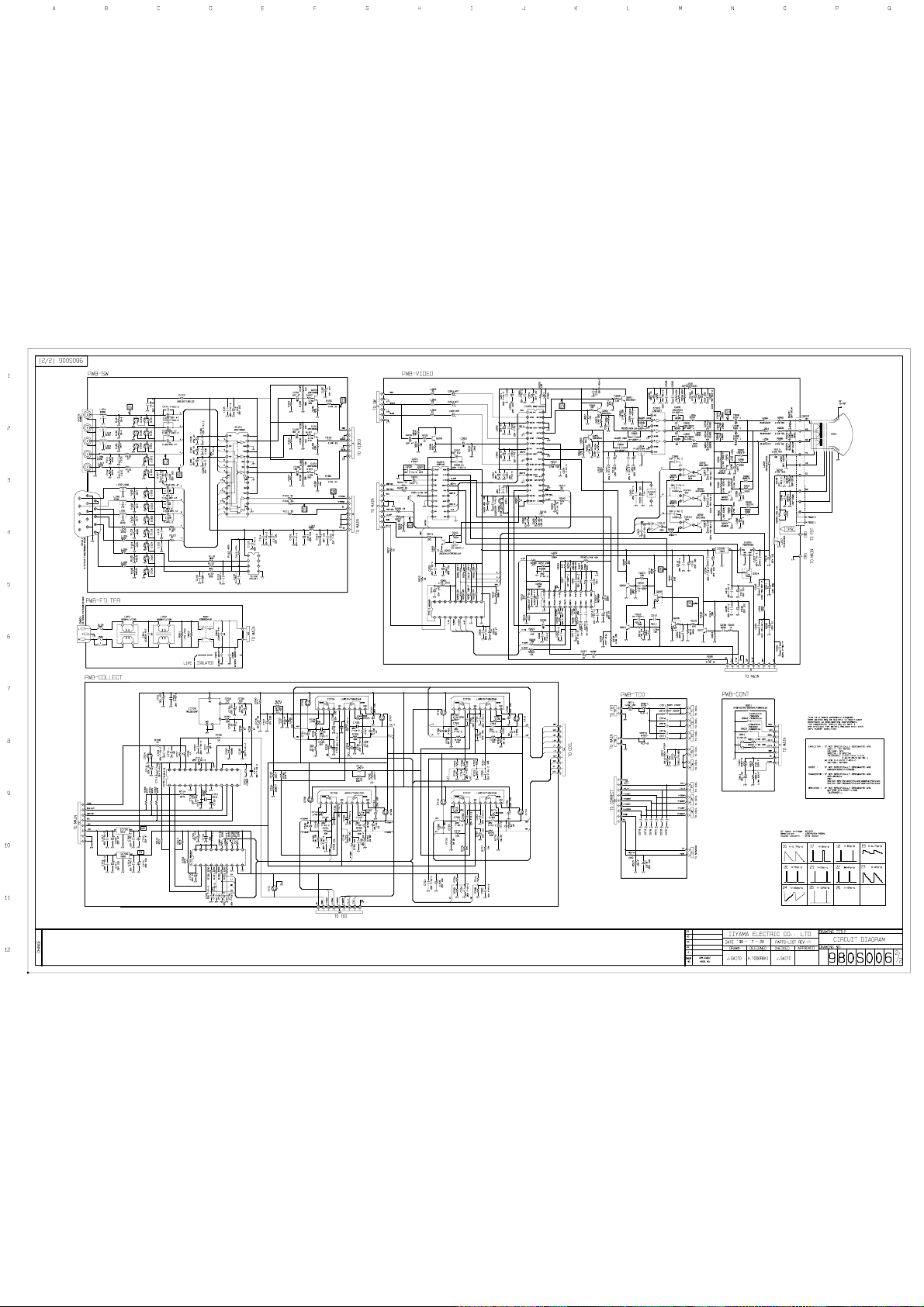
 Loading...