

Page 1

Device manual
Original Scale Drawing (MTD)
ioControl
CR2050
CR2051
CR2052
UK
80268387 / 00 04 / 2018
Page 2

ioControl
Contents
1 Preliminary note � � � � � � � � � � � � � � � � � � � � � � � � � � � � � � � � � � � � � � � � � � � � � � � � � 4
1�1 Explanation of symbols � � � � � � � � � � � � � � � � � � � � � � � � � � � � � � � � � � � � � � � 4
2 Safety instructions � � � � � � � � � � � � � � � � � � � � � � � � � � � � � � � � � � � � � � � � � � � � � � � 4
2�1 General safety instructions � � � � � � � � � � � � � � � � � � � � � � � � � � � � � � � � � � � � � 4
2�2 Target group � � � � � � � � � � � � � � � � � � � � � � � � � � � � � � � � � � � � � � � � � � � � � � � � 5
2�3 Electrical connection � � � � � � � � � � � � � � � � � � � � � � � � � � � � � � � � � � � � � � � � � 5
2�4 Tampering with the unit � � � � � � � � � � � � � � � � � � � � � � � � � � � � � � � � � � � � � � � 6
3 Functions and features � � � � � � � � � � � � � � � � � � � � � � � � � � � � � � � � � � � � � � � � � � � � 6
4 Function � � � � � � � � � � � � � � � � � � � � � � � � � � � � � � � � � � � � � � � � � � � � � � � � � � � � � � � 7
5 Installation� � � � � � � � � � � � � � � � � � � � � � � � � � � � � � � � � � � � � � � � � � � � � � � � � � � � � � 7
5�1 Mounting surface � � � � � � � � � � � � � � � � � � � � � � � � � � � � � � � � � � � � � � � � � � � � 7
5�2 Fixing � � � � � � � � � � � � � � � � � � � � � � � � � � � � � � � � � � � � � � � � � � � � � � � � � � � � � 7
5�3 Cable seal � � � � � � � � � � � � � � � � � � � � � � � � � � � � � � � � � � � � � � � � � � � � � � � � � 8
6 Electrical connection� � � � � � � � � � � � � � � � � � � � � � � � � � � � � � � � � � � � � � � � � � � � � � 9
6�1 General electrical connection � � � � � � � � � � � � � � � � � � � � � � � � � � � � � � � � � � 9
6�2 Connection accessories � � � � � � � � � � � � � � � � � � � � � � � � � � � � � � � � � � � � � � 10
6�3 Frequency inputs � � � � � � � � � � � � � � � � � � � � � � � � � � � � � � � � � � � � � � � � � � � 10
6�4 Reverse polarity protection� � � � � � � � � � � � � � � � � � � � � � � � � � � � � � � � � � � � 10
6�5 Supply of the signal generators at the inputs � � � � � � � � � � � � � � � � � � � � � 10
6�6 Fuses � � � � � � � � � � � � � � � � � � � � � � � � � � � � � � � � � � � � � � � � � � � � � � � � � � � � 10
6�7 Examples for connection types � � � � � � � � � � � � � � � � � � � � � � � � � � � � � � � � �11
6�7�1 CR2050 � � � � � � � � � � � � � � � � � � � � � � � � � � � � � � � � � � � � � � � � � � � � � � �11
6�7�2 CR2051 � � � � � � � � � � � � � � � � � � � � � � � � � � � � � � � � � � � � � � � � � � � � � � 12
6�7�3 CR2052 � � � � � � � � � � � � � � � � � � � � � � � � � � � � � � � � � � � � � � � � � � � � � � 13
7 Operating and display elements � � � � � � � � � � � � � � � � � � � � � � � � � � � � � � � � � � � � 14
7�1 Menu structure � � � � � � � � � � � � � � � � � � � � � � � � � � � � � � � � � � � � � � � � � � � � � 15
7�2 Status indication of the inputs/outputs (I/O LEDs, yellow) � � � � � � � � � � � � 16
8 Set-up � � � � � � � � � � � � � � � � � � � � � � � � � � � � � � � � � � � � � � � � � � � � � � � � � � � � � � � 17
8�1 I/O module � � � � � � � � � � � � � � � � � � � � � � � � � � � � � � � � � � � � � � � � � � � � � � � � 17
8�1�1 Display mode � � � � � � � � � � � � � � � � � � � � � � � � � � � � � � � � � � � � � � � � � � 17
8�1�2 Parameter setting� � � � � � � � � � � � � � � � � � � � � � � � � � � � � � � � � � � � � � � 17
8�1�3 List of parameters � � � � � � � � � � � � � � � � � � � � � � � � � � � � � � � � � � � � � � 18
8�2 Controller � � � � � � � � � � � � � � � � � � � � � � � � � � � � � � � � � � � � � � � � � � � � � � � � � 19
8�2�1 Programming � � � � � � � � � � � � � � � � � � � � � � � � � � � � � � � � � � � � � � � � � � 19
8�3 Required documentation � � � � � � � � � � � � � � � � � � � � � � � � � � � � � � � � � � � � � 19
8�4 Required hardware � � � � � � � � � � � � � � � � � � � � � � � � � � � � � � � � � � � � � � � � � � 19
9 Technical data� � � � � � � � � � � � � � � � � � � � � � � � � � � � � � � � � � � � � � � � � � � � � � � � � � 20
9�1 CR2050 � � � � � � � � � � � � � � � � � � � � � � � � � � � � � � � � � � � � � � � � � � � � � � � � � � 20
9�2 CR2051 � � � � � � � � � � � � � � � � � � � � � � � � � � � � � � � � � � � � � � � � � � � � � � � � � � 26
9�3 CR2052 � � � � � � � � � � � � � � � � � � � � � � � � � � � � � � � � � � � � � � � � � � � � � � � � � � 32
2
Page 3

ioControl
10 Maintenance, repair and disposal� � � � � � � � � � � � � � � � � � � � � � � � � � � � � � � � � � 39
10�1 Maintenance� � � � � � � � � � � � � � � � � � � � � � � � � � � � � � � � � � � � � � � � � � � � � � 39
10�2 Cleaning the housing surface � � � � � � � � � � � � � � � � � � � � � � � � � � � � � � � � � 39
10�3 Repair� � � � � � � � � � � � � � � � � � � � � � � � � � � � � � � � � � � � � � � � � � � � � � � � � � � 39
10�4 Disposal � � � � � � � � � � � � � � � � � � � � � � � � � � � � � � � � � � � � � � � � � � � � � � � � � 39
11 Approvals/standards � � � � � � � � � � � � � � � � � � � � � � � � � � � � � � � � � � � � � � � � � � � � 39
12 Appendix� � � � � � � � � � � � � � � � � � � � � � � � � � � � � � � � � � � � � � � � � � � � � � � � � � � � � 40
12�1 EMCY Object � � � � � � � � � � � � � � � � � � � � � � � � � � � � � � � � � � � � � � � � � � � � � 40
12�2 Object directory CR205x � � � � � � � � � � � � � � � � � � � � � � � � � � � � � � � � � � � � 40
12�2�1 Device-specific CR2050� � � � � � � � � � � � � � � � � � � � � � � � � � � � � � � � � 44
12�2�2 Device-specific CR2051� � � � � � � � � � � � � � � � � � � � � � � � � � � � � � � � � 65
12�2�3 Device-specific CR2052� � � � � � � � � � � � � � � � � � � � � � � � � � � � � � � � � 89
12�3 SDOs error messages � � � � � � � � � � � � � � � � � � � � � � � � � � � � � � � � � � � � � 121
12�3�1 CR2050 � � � � � � � � � � � � � � � � � � � � � � � � � � � � � � � � � � � � � � � � � � � � 121
12�3�2 CR2051 � � � � � � � � � � � � � � � � � � � � � � � � � � � � � � � � � � � � � � � � � � � � 123
12�3�3 CR2052 � � � � � � � � � � � � � � � � � � � � � � � � � � � � � � � � � � � � � � � � � � � � 125
UK
This document is the original instructions�
All trademarks and company names used are subject to the copyright of the respective companies�
3
Page 4
ioControl
1 Preliminary note
This document applies to devices of the type "ioControl" (art� no�: CR2050,
CR2051 and CR2052)�
It is part of the device�
The document contains information about the correct handling of the device�
Adhere to the safety instructions�
Technical data, approvals, accessories and further information at:
www�ifm�com�
1.1 Explanation of symbols
► Instructions
> Reaction, result
[…] Designation of keys, buttons or indications
→ Cross-reference
Important note
Non-compliance may result in malfunction or interference�
Information
Supplementary note
WARNING
Warning of serious personal injury�
Death or serious irreversible injuries may result�
CAUTION
Warning of personal injury�
Slight reversible injuries may result�
NOTE
Warning of damage to property�
2 Safety instructions
2.1 General safety instructions
● Read this document before setting up the device and keep it during the entire
service life�
● Ensure that the product is suitable for your application and operating conditions
without any restrictions�
4
Page 5

ioControl
● Improper or non-intended use may lead to malfunctions of the unit, to
unwanted effects in the application or to a loss of the warranty claims�The
manufacturer assumes no liability for any consequences caused by tampering
with the device or incorrect use by the operator�
● Installation, electrical connection, set-up, operation and maintenance of the
unit must be carried out by qualified personnel authorised and trained by the
machine operator�
● After installation, maintenance or repair of the system perform a complete
function check�
● The system installer is responsible for the safety of the system into which the
device is integrated�
2.2 Target group
These instructions are intended for authorised persons according to the EMC
and low-voltage directives� The device must be installed, connected and put into
operation by a qualified electrician�
UK
2.3 Electrical connection
WARNING
Disconnect the device externally before handling it�
Supply via a mobile on-board system 12/24V battery voltage or safety extra-low
voltage (SELV) according to the technical data� The supply is directly transferred to
the connected sensors/actuators�
Accessible surfaces of the housing are insulated from the circuits with basic
insulation to IEC 61010-1, secondary circuit with max� 32 V DC, supplied from
main circuit up to 300 V of overvoltage category II�
The external wiring has to be carried out in a way that ensures the required
separation from other circuits�
The cable cross section is to be adapted to the fuse used, taking into account the
applicable regulations for the application�
The wiring has to be suitable for the max� temperature reached in the application�
If the supplied SELV voltage is externally grounded (SELV becomes PELV), the
responsibility lies with the user and the respective national installation regulations
must be complied with�
The connections may only be supplied with the signals indicated in the technical
data and/or on the device label and only the approved accessories of ifm
electronic gmbh may be connected�
5
Page 6

ioControl
2.4 Tampering with the unit
WARNING
In case of malfunctions or uncertainties please contact the manufacturer� Any
tampering with the device can seriously affect the safety of operators and
machinery�
3 Functions and features
The freely programmable controllers of the "ioControl" series are rated for use
under difficult conditions (e�g� extended temperature range, strong vibration,
intensive EMC interference)� They are suitable for direct installation in mobile
machines, even in wet environments�
By means of the application software the user can configure the inputs and outputs
to adapt to the respective application� The controllers can be used as CANopen
slave, CANopen master or intelligent I/O module (→ 9 Technical data)�
Application-specific extensions and adaptations are possible in conjunction with
additional products of the modular ioControl and ecomatmobile Basic design�
WARNING
The "ioControl" series is not approved for safety tasks in the field of safety of
persons�
NOTE
The "ioControl" controllers are intended for installation in vehicle bodies, not in
engines�
NOTE
The device must only be used within the limits indicated in the technical data
(→ 9 Technical data)� If the device is used in a way that is not intended by the
manufacturer, the protection supported by the device may be impaired�
6
Page 7
ioControl
4 Function
● The user can easily create the application software by means of the IEC 61131-
3 compliant programming system CODESYS 2�3� On delivery the devices are
pre-configured as CANopen slaves�
● 2 CAN interfaces
● Configurable inputs/outputs
● Status LEDs, I/O Leds and 4-digit 10-segment display
● Operating keys
More information and accessories at www�ifm�com�
5 Installation
5.1 Mounting surface
NOTE
The housing must not be exposed to any torsional forces or mechanical stress�
► Mount the device on a flat surface�
► Use compensating elements if there is no flat mounting surface available�
UK
Mounting surface
5.2 Fixing
► Insert the enclosed tubular rivets from the back of the module in the 3 fixing
holes�
► Fix the device using 3 washers and M5 screws�
Tighten the screws alternately�
7
Page 8
ioControl
Use of the tubular rivets
Tightening torque: 2�0 Nm
Hole dimensions (→ 9 Technical data)
Screws to be used (examples): Standard
Cylinder screws with hexagon socket (M5 x L) DIN EN ISO 4762
Cylinder screws with hexagon socket and low head (M5 x L) DIN 7984
5.3 Cable seal
NOTE
Protection rating IP 65 / IP 67 is only guaranteed if all ports are sealed by means
of connectors or dummy plugs�
8
Page 9

ioControl
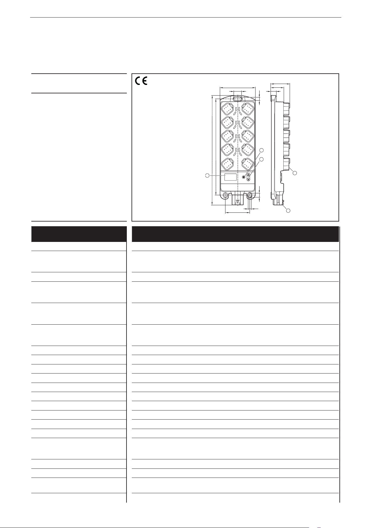
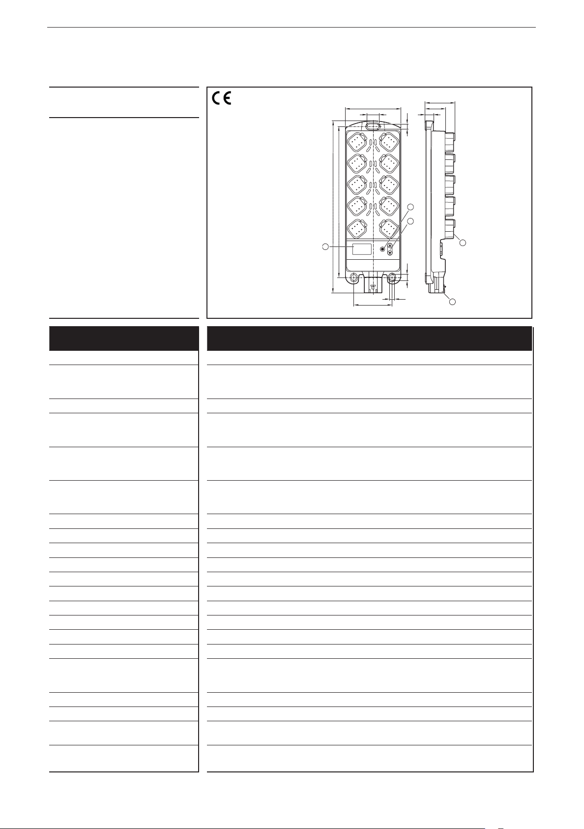
Original Scale Drawing (MTD)
1
3
5
6
7
2
4
878
9
10
11
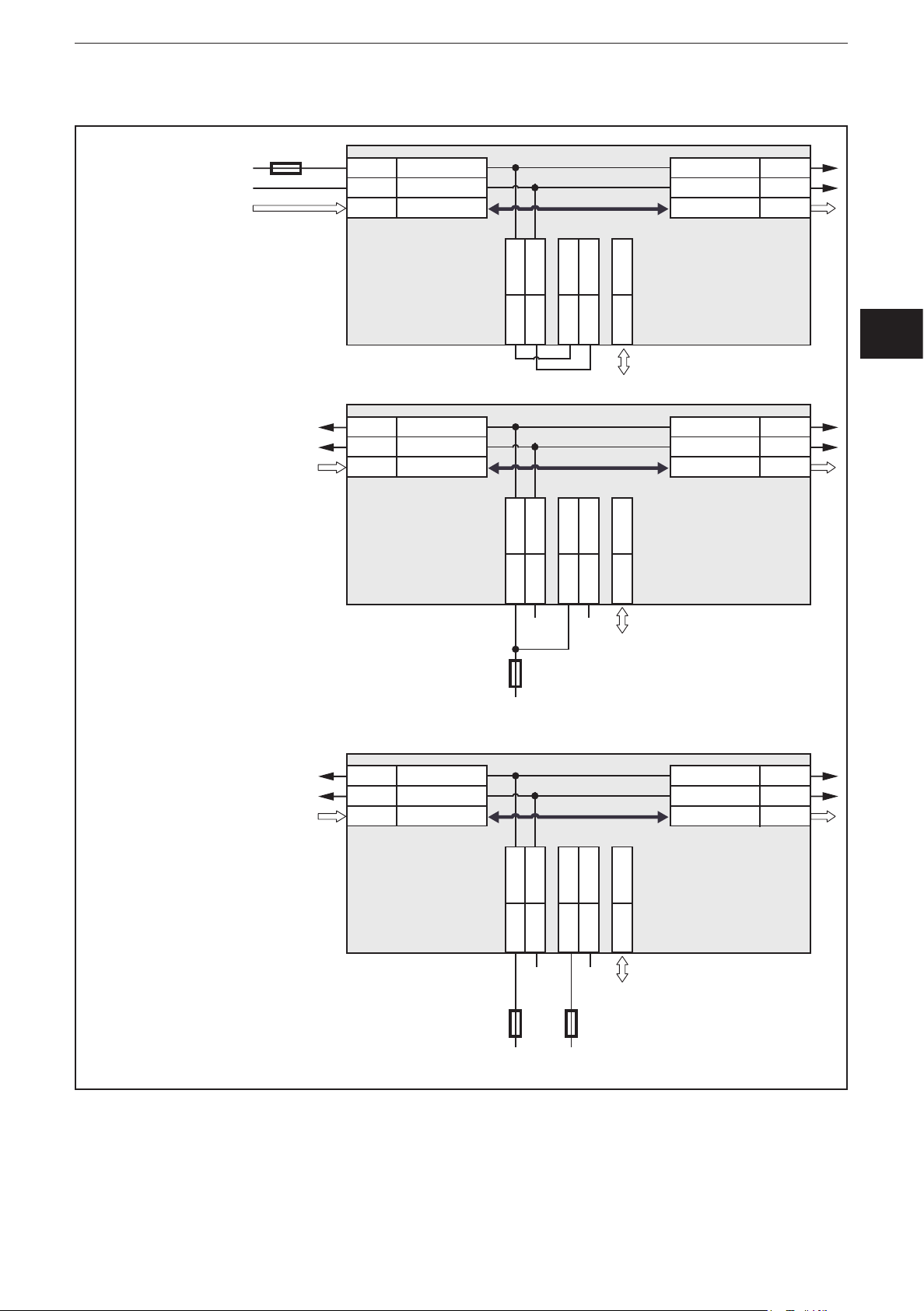
6 Electrical connection
6.1 General electrical connection
The supply cables and the CAN2 interface are connected via the X1 connector
on the bottom of the device� The inputs/outputs, the CAN1 interface and the CAN
supply are connected via the Deutsch connectors on the front side of the housing�
Wiring (→ 9 Technical data)
1: Connector 8
2: Connector 6
3: Connector 4
4: Connection 2
Connector area (here e�g� CR0403)
5: CAN1 OUT
6: X1 - Connection cable plug
7: CAN1 IN
8: Connector 1
9: Connector 3
10: Connector 5
11: Connector 7
9
UK
Connector CR2050 CR2051 CR2052 Number
of poles
1 IN00 / IN08 OUT00 / OUT08 IN00 / IN04 6
2 IN01 / IN09 OUT01 / OUT09 OUT00 / OUT04 6
3 IN02 / IN10 OUT02 / OUT10 IN01 / IN05 6
4 IN03 / IN11 OUT03 / OUT11 OUT01 / OUT05 6
5 IN04 / IN12 OUT04 / OUT12 IN02 / IN06 6
6 IN05 / IN13 OUT05 / OUT13 OUT02 / OUT06 6
7 IN06 / IN14 OUT06 / OUT14 IN03 / IN07 6
8 IN07 / IN15 OUT07 / OUT15 OUT03 / OUT07 6
CAN1 IN CAN1 interface 6
CAN1 OUT CAN1 interface (e�g� for looping through) 6
X1 Supply voltage and CAN2 interface 6
NOTE
Wrong connection may cause damage to the device�
► Observe the safety instructions (→ 2.3 Electrical connection)�
9
Page 10

ioControl
► Basically all supply and signal cables must be laid separately�
► Lay supply and signal cables away from the device using the shortest possible
route�
► All connected cables must be provided with a strain relief max� 400 mm behind
the cable entry�
► Cover unused terminals with dummy plugs / seals�
6.2 Connection accessories
Information about the available accessories at www�ifm�com
6.3 Frequency inputs
CR2050 / CR2052:
► Operate frequency inputs with screened cables so that useful signals are not
affected by external interference�
6.4 Reverse polarity protection
Reverse polarity protection of the operating voltage is only ensured in case of
operation on an on-board system in connection with a fuse� In case of operation
via a power supply, there is no reverse polarity protection of the operating voltage�
CR2051: There is no reverse polarity protection of the CAN supply voltage, as this
voltage is not used within the device�
6.5 Supply of the signal generators at the inputs
CR2050 / CR2052:
► Use sensor voltage VBBS of the corresponding connector as supply voltage for
the signal generators at the inputs (e�g� switches or sensors)�
► If the input (switch or sensor) is supplied via an external voltage, protect this
voltage with max� 3 A�
6.6 Fuses
► The individual electric circuits must be protected in order to protect the whole
system�
Designation Potential Connector: Pin Fuse
VBBSSupply sensors/module 8���32 V DC AMP connector:
Pin 4
VBB1Supply outputs
CR2050: not available
CR2051: OUT00, 02, 04, 06, 08, 10, 12, 14
CR2052: not available
VBB2Supply outputs
CR2050: not available
CR2051: OUT01, 03, 05, 07, 09, 11, 13, 15
CR2052: OUT00���07
10
8���32 V DC AMP connector:
Pin 4
8���32 V DC AMP connector:
Pin 6
CR2050: 3 A
CR2052: 3 A
CR2050: CR2051: ≤ 25 A
CR2052: -
CR2050: -
CR2051: ≤ 25 A
CR2052: ≤ 25 A
Page 11

Designation Potential Connector: Pin Fuse
Supply
3 A
Supply
ioControl
V
CAN
Optional supply CAN1 interface
CR2050: connected to VBBS
CR2051: no connection to VBBS
CR2052: connected to VBB
S
8���32 V DC CAN IN: Pins 3+4
CR2050: CR2051: 3 A
CR2052: -
► Connect the ground pins belonging to the supply voltages (GND1, GND2, if
appl� GND
) to the common ground�
CAN
6.7 Examples for connection types
6.7.1 CR2050
Example 1
CAN loop,
supply via
CAN IN
03/04 V
01/06 GND
02/05
CAN
CAN
CAN1
CAN IN CAN OUT
*
S
VBB
GND1n.c.
CR2050
01
04
06
03 n.c.
02/05 CAN2
CAN
V
CAN
GND
CAN1
* Load-Dump
Protection
UK
03/04
01/06
02/05
Example 2
Supply via
connectorX1
n.c. n.c.
03/04 V
01/06 GND
02/05
CAN
CAN
CAN1
CAN IN CAN OUT
*
S
VBB
GND1n.c.
GND
CAN1
CR2050
01
04
3 A
06
n.c.
03 n.c.
02/05 CAN2
CAN
CAN
03/04V
01/06
02/05
* Load-Dump
Protection
11
Page 12
ioControl
Supply
3 A
Supply
Supply
Supply
6.7.2 CR2051
Example 1
CAN loop, low
load, supply
via CAN IN
Example 2
medium load,
common fuse
**additional
protection
required if
common fuse
> 3 A
3 A**
GND
03/04 V
01/06 GND
02/05
CAN
CAN
GND
CAN1
CAN IN CAN OUT
/
*
S
1
VBB
VBB
GND1VBB2GND
2
CAN2
CR2051
06
03/04 V
CAN
01/06 GND
CAN
04
01
03
02/05
GND
02/05 CAN1
CAN IN CAN OUT
/
*
S
1
VBB
VBB
GND1VBB2GND
2
CAN2
CR2051
06
04
GND
01
GND
03
02/05
CAN
CAN1
CAN
03/04V
01/06
02/05
* Load-Dump
Protection
CAN
CAN1
CAN
03/04V
01/06
02/05
* Load-Dump
Protection
max. 25 A
Supply
Example 3
max. load
3 A
03/04 V
01/06 GND
02/05
CR2051
CAN
CAN
CAN1
CAN IN CAN OUT
/
*
S
1
VBB
VBB
GND1VBB2GND
2
CAN2
CAN
CAN
GND
CAN1
* Load-Dump
03/04V
01/06
02/05
Protection
04
01
03
02/05
06
GND GND
15...25 A
max. 25 A
Protection against overvoltage from the vehicle's on-board system is only ensured
if the connection VBBS/VBB1 is protected with at least 15 A (example 3) or if all
voltages are protected by means of a common fuse (examples 1 and 2)�
12
Page 13
6.7.3 CR2052
Supply
3 A
Supply
Supply
ioControl
Example 1
CAN loop, low
load, supply
via CAN IN
Example 2
low load,
common fuse
03/04 V
01/06 GND
02/05
CAN
CAN
GND
CAN1
CAN IN CAN OUT
S
VBB
1
GND
*
2
VBB
2
CR2052
01
04
03/04 V
01/06 GND
02/05
CAN
CAN
CAN1
CAN IN CAN OUT
S
VBB
1
GND
06
*
2
VBB
03 GND
2
02/05 CAN2
GND
CR2052
01
04
06
03 GND
02/05 CAN2
CAN
V
CAN1
CAN
03/04
01/06
02/05
* Load-Dump
Protection
CAN
V
CAN1
CAN
03/04
01/06
02/05
* Load-Dump
Protection
UK
Example 3
max. load
GND GND
3 A
Supply
03/04 V
01/06 GND
02/05
CAN
CAN
GND
CAN1
CAN IN CAN OUT
S
VBB
1
GND
*
2
VBB
2
CR2052
01
04
GND
3 A
06
03 GND
GND
15...25 A
02/05 CAN2
CAN
V
CAN1
CAN
03/04
01/06
02/05
* Load-Dump
Protection
Protection against overvoltage from the vehicle's on-board system is only ensured
if the connection VBB2 is protected with at least 15 A (example 3) or if all voltages
are protected by means of a common fuse (examples 1 and 2)�
13
Page 14
ioControl
Original Scale Drawing (MTD)
Original Scale Drawing (MTD)
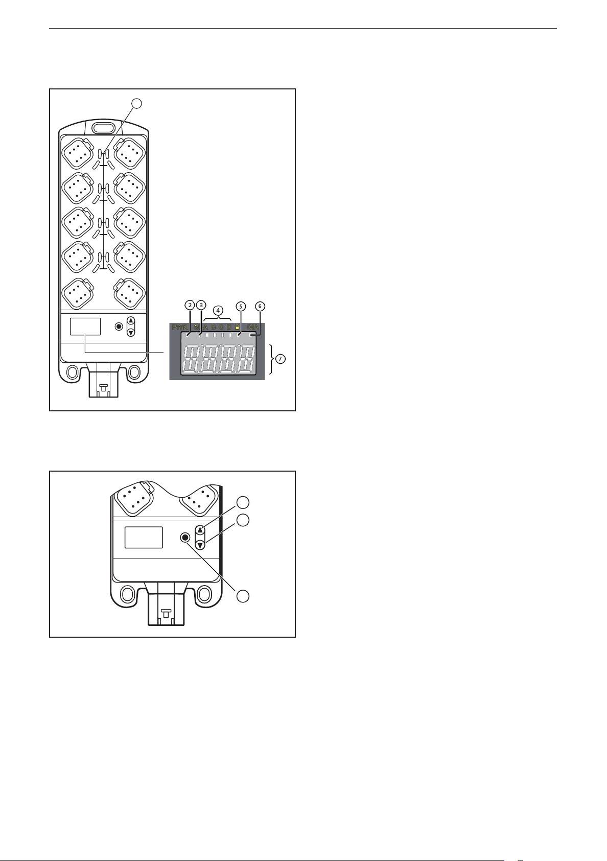
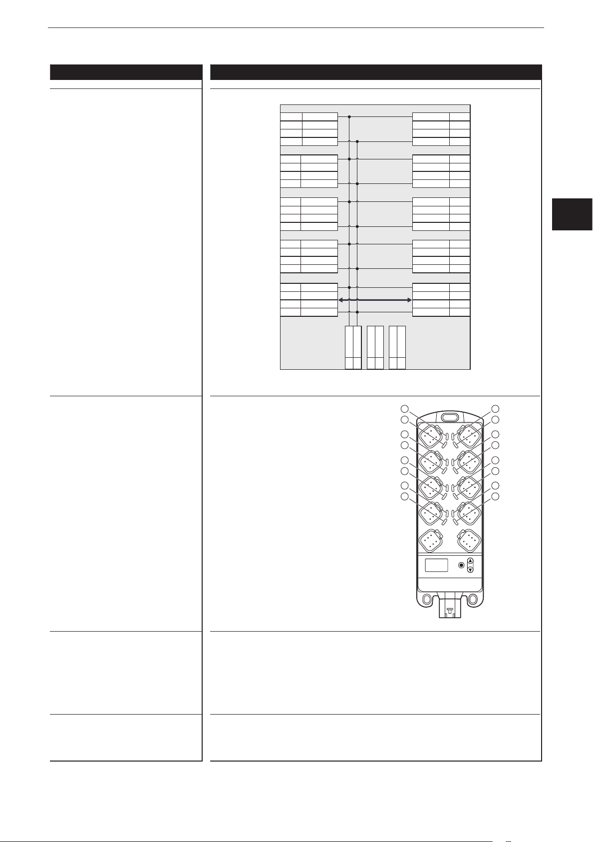
7 Operating and display elements
1
8
7
6
5
4
3
1 2
Indicators
10-segment display (→ 9 Technical data)
1
2
3
1: I/O LEDs (yellow)
2: Power LED (green)
3: Mode LED (green)
4: Application LEDs LED A���LED D (green)
5: Lock LED (green)
6: Diagnostics LED (red)
7: 4-digit 10-segment display
1: UP button
2: DOWN button
3: ENTER button
Operating elements
Pushbutton functions (→ 8.1 I/O module)�
14
Page 15

7.1 Menu structure
The following description of the menu structure refers to the factory
setting as I/O module� When the device is configured as a controller, the
corresponding menu structure has to be defined (see system manual
ioControl)�
1
ioControl
Node ID
Baud rate
Error code 1
Error code 2
Error code 3
Error code 4
+
>10 s
nodE
BAUD
>10 s
uLoc
+
-123
-123
-123
20
50
100
125
250
500
2
UK
1...125
1: Display mode (→ 8.1.1)
2: Editing mode (→ 8.1.2)
List of parameters: (→ 8.1.3)
800
1000
1
Loc
15
Page 16

ioControl
7.2 Status indication of the inputs/outputs (I/O LEDs, yellow)
I/O configuration
(see attached object directory)
0 (not used) Off
1 (digital input BL) Off Input signal FALSE
2 (digital output BH) Off Output signal FALSE
3 (voltage input 10 V) Off
4 (PWM output) Off PWM = 0
5 (current-controlled output) Off Current value ≤ 20 mA
6 (voltage input 32 V, ratiometric) Off
7 (current input 20 mA) Off
LED status Description
On Input signal TRUE
On Output signal TRUE
On PWM > 0
On Current value ≤ 20 mA
2 Hz Fault at the input
9 (voltage input 32 V) Off
10 (digital input BL) Off Input signal FALSE
On Input signal TRUE
11 (digital input BL, mit Diagnose) Off Input signal FALSE
On Input signal TRUE
2 Hz Fault at the input
12 (digital input BH) Off Input signal FALSE
On Input signal TRUE
14 (frequency input) Off
2 Hz Fault at the input
15 (digital output BH, with diagnostics) Off Output signal FALSE
On Output signal TRUE
2 Hz Fault at the output
16 (digital output BH, with diagnostics,
short-circuit proof and overload protected)
Off Output signal FALSE
On Output signal TRUE
2 Hz Fault at the output
18 (resistor input) Off
20 (interval measurement) Off
16
2 Hz Fault at the input
2 Hz Fault at the input
Page 17

ioControl
8 Set-up
8.1 I/O module
On delivery the device is configured as I/O module�
After power on the 10-segment display indicates the article number of the device,
followed by the set node ID�
8.1.1 Display mode
If the green Lock LED is on, the device is in display mode� The device can only
indicate the set node ID and baud rate and, if appl�, error messages; parameters
cannot be edited�
► Press the DOWN button�
> The device displays the set baud rate�
► Press the DOWN button�
> The device displays error code 1, if applicable�
► Press the DOWN button again�
> Every time the DOWN button is pressed, the device displays another error
code, if applicable�
► Use the UP button to go back�
Max� 4 different error codes can occur and be displayed:
Error code Description
SH Short circuit to GND
UK
OP Wire break
oL Excessive current
Comm Communication error
If no button is activated for 10 s, the device displays the set node ID�
8.1.2 Parameter setting
► Press UP and DOWN simultaneously for at least 10 s to change to the editing
mode�
> Green Lock LED goes out�
> Parameters can be edited�
> "uLoc" is displayed for 5 s
> "nodE" is displayed
► Press the ENTER button�
> The device displays the set node ID�
17
Page 18

ioControl
> The 1st digit to be edited flashes�
► Use the UP and DOWN buttons to set the requested value�
► Use the ENTER button to go to the next digit�
> The 2nd digit to be edited flashes�
► Use the UP and DOWN buttons to set the requested value�
► Use the ENTER button to go to the next digit�
> The 3rd digit to be edited flashes�
► Use the UP and DOWN buttons to set the requested value�
► Press the ENTER button�
> The set node ID is confirmed�
> "nodE" is displayed
► Press the DOWN button�
> "BAUD" is displayed
► Press the ENTER button�
> The device displays the set baud rate�
► Use the UP and DOWN buttons to set the requested value�
► Press the ENTER button�
> The set baud rate is confirmed�
Changes of the parameters are only applied after a reset of the device�
Exit the editing mode:
► Press UP and DOWN simultaneously for at least 10 s�
> Green Lock LED on�
> Parameters cannot be edited�
> "Loc" is displayed for 5 s, then the set node ID is displayed
If no button is activated for 30 s, the device automatically finishes the editing
mode�
8.1.3 List of parameters
Parameters Function Value range Default value
nodE Node ID of the device 1���125 125
BAUD Baud rate 20, 50, 100, 125, 250, 500, 800, 1000 250 kBit/s
18
Page 19

ioControl
8.2 Controller
The device can be configured as a controller� The existing menu structure and the
properties as I/O module will be lost�
8.2.1 Programming
The user can easily create the application software by means of the IEC 61131-3
compliant programming system CODESYS 2�3�
WARNING
The user is responsible for the safe function of the application programs which
he created himself� If necessary, he must additionally carry out an approval
by corresponding supervisory and test organisations according to the national
regulations�
UK
For notes on the setting of the CAN ID and the baud rate when used as
CANopen slave, refer to the system manual�
8.3 Required documentation
In addition to the CODESYS programming system, the following documents are
required for programming and set-up of the device:
● Programming manual CODESYS V2�3
(alternatively as online help)
● System manual ioControl
(alternatively as online help)
The manuals can be downloaded from the internet:
www�ifm�com
8.4 Required hardware
If used as mobile controller a CAN interface for connection to a PC or notebook is
required to load the application program to the device�
Example:
● CAN/RS232 USB interface CANfox
● Adapter cable for CANfox
You can find more information about the available accessories at:
www�ifm�com
19
Page 20
ioControl
Control systems
Original Scale Drawing (MTD)
9 Technical data
9.1 CR2050
CR2050
I/O module
digital and analogue
for R360 system
CANopen slave
Mobile controller
Programming
to IEC 61131-3
16 inputs
2 CAN interfaces
8���32 V DC
1: ENTER button
76
17
8
7
6
5
4
3
205,5
234,2
3
1 2
40,5
27,4
11
6,9
1
2
4
8,7
2: UP/DOWN buttons
3: 10-segment display
4: DEUTSCH connector
6,9
52
5
5: AMP connector
Technical data Modular control system
Usable as CANopen slave or intelligent I/O module
Mechanical data
Housing Housing: PA6/6�6
Display: PA
Pushbuttons: silicone
Dimensions (H x W x D) 234 x 76 x 40�5 mm (without tubular rivet)
Installation Fixing by means of 3 M5 screws to DIN EN ISO 4762 or DIN 7984, 3 tubular
rivets to DIN 7340 and 3 washers to DIN EN ISO 7092 (tubular rivets and
washers are supplied)
Connection Supply: MCP2�8 6 poles for connector TE-AMP 1745078-1
Inputs/outputs: Deutsch DT04-6S 6 poles
Contacts: AMP: CuFe tin-plated; Deutsch: CuZn, gold-plated
Inputs
CAN1 interface
Operating voltage, CAN2
8 x 6 poles
2 x 6 poles
1 x 6-poles
Protection rating IP 65 and IP 67 (all connectors inserted)
Operating/storage temperature -40���85° C / -40���85° C
Max� perm� relative humidity 90%, non condensing
Max� height above sea level 2000 m
Pollution degree 2
Weight 500 g
Electrical data
Operating voltage 8���32 V DC
Current consumption 100 mA (at 24 V DC) / 185 mA (at 12 V DC) / max� 300 mA
Overvoltage
Undervoltage detection
Undervoltage shutdown
36 V for t ≤ 10 s
≤ 7.8 V
if U
B
if U
≤ 7.0 V
B
Processor Freescale PowerPC, 50 MHz
Memory (total) 592 Kbytes RAM / 1536 Kbytes Flash / 1 Kbyte FRAM
Memory allocation See system manual ioControl and
www�ifm�com
20
Page 21

CR2050 Technical data
Control systems
Device monitoring Undervoltage monitoring
Watchdog function
Checksum test for program and system
Excess temperature monitoring
CAN interfaces 1 and 2
Baud rate
Communication protocol
20 Kbits/s…1 Mbits/s (default CAN1: 250 Kbits/s, CAN2: 250 Kbits/s)
CANopen, CiA DS 301 version 4, CiA DS 401 version 1�4
CAN interface 2�0 A/B, ISO 11898
or SAE J 1939 or free protocol
Software/Programming
Programming system CODESYS version 2�3 (IEC 61131-3)
Inputs 16 (confi gurable)
Confi gurations
Number Description
8 digital for positive / negative sensor signals
analogue (0…10/32 V DC, 0���20 mA, ratiometric)
ioControl
B
L/BH
A
UK
4 digital for positive sensor signals
resistance measurement (0.016...30 kΩ)
4 digital for positive sensor signals
digital for negative sensor signals*
frequency (≤ 30 kHz)
* not available in the I/O module (CANopen slave)
Indicators
I/O LEDs 16 x LED orange
(default setting: status indication of the corresponding input)
Power LED (PWR) LED green
(default setting: indication of the system status)
Mode LED (M) LED green
(default setting: indicates that the node ID is displayed)
Application LEDs (A���D) 4 x LED green
Lock LED (lock symbol) 1 x LED green
(default setting: locking of the set parameters)
Diagnostics LED (DIA) 1 x LED red
(default setting: indication of an error)
Display 4-digit 10-segment display (two colours: red/green)
(default setting: indication of the baud rate or the node ID)
Operating states when used as mobile
controller
LED State Description
– Permanently off No operating voltage
PWR + DIA 1 x on Initialisation or reset checks
PWR 5 Hz No operating system loaded
2 Hz Application running (RUN)
Permanently on Application stopped (STOP)
DIA 10 Hz Application stopped (STOP with error)
5 Hz Application stopped due to undervoltage
Permanently on System error (fatal error)
B
L
R
B
L
B
H
FRQ
ifm electronic gmbh • Friedrichstraße 1 • 45128 Essen
We reserve the right to make technical alterations without prior notice! 20 April 2018CR2050 / page 2
21
Page 22

ioControl
Control systems
CR2050 Technical data
Operating elements
Pushbuttons ENTER, UP, DOWN
Pushbuttons (default setting) Setting of the CAN ID / baud rate
Input characteristics
Analogue inputs (B
IN00 - Connection 1, Pin 5
IN01 - Connection 2, Pin 5
IN02 - Connection 3, Pin 5
IN03 - Connection 4, Pin 5
IN04 - Connection 5, Pin 5
IN05 - Connection 6, Pin 5
IN06 - Connection 7, Pin 5
IN07 - Connection 8, Pin 5
can be confi gured as...
, BH, A)
L
● Voltage inputs
Input voltage 0���10 V or 0���32 V
Resolution 12 bits
Accuracy ± 1% FS
Input resistance 65.6 kΩ (0...10 V), 50.7 kΩ (0...32 V)
Input frequency ≤ 500 Hz
● Current inputs, with diagnostic capability
Input current 0 … 20 mA
Resolution 12 bits
Accuracy ± 1% FS
Input resistance 400 Ω
Input frequency ≤ 500 Hz
At a current of > 23 mA the input is switched to the voltage input!
● Voltage inputs, 0���32 V, ratiometric
Function (U
÷ UB) x 1000 ‰
IN
Value range 0���1000 ‰
Input resistance 50.7 kΩ
● Binary voltage inputs for positive sensor signals
Switch-on level
Switch-off level < 0�3 U
> 0�7 U
B
B
Input resistance 3.2 kΩ
Input frequency 50 Hz
Diagnostics wire break
> 0�95 U
B
Diagnostics short circuit < 1 V
● Binary voltage inputs for negative sensor signals
Switch-on level
Switch-off level < 0�3 U
> 0�7 U
B
B
Input resistance 3.2 kΩ
Input frequency 50 Hz
Digital inputs (B
L
, R)
IN08 - Connection 1, Pin 2
IN10 - Connection 3, Pin 2
IN12 - Connection 5, Pin 2
IN14 - Connection 7, Pin 2
can be confi gured as...
ifm electronic gmbh • Friedrichstraße 1 • 45128 Essen
● Binary voltage inputs for positive sensor signals
Switch-on level
Switch-off level < 0�3 U
> 0�7 U
B
B
Input resistance 3.2 kΩ
Input frequency 50 Hz
Diagnostics wire break
> 0�95 U
B
Diagnostics short circuit < 1 V
● Resistor input
Measuring range 0.016…30 kΩ
Accuracy ± 2% FS: 16 Ω...3 kΩ
± 5 % FS: 3...15 kΩ
± 10 % FS: 15...30 kΩ
We reserve the right to make technical alterations without prior notice! 20 April 2018CR2050 / page 3
22
Page 23

CR2050 Technical data
Control systems
Frequency inputs (BL, BH, FRQ)
IN09 - Connection 2, Pin 2
IN11 - Connection 4, Pin 2
IN13 - Connection 6, Pin 2
IN15 - Connection 8, Pin 2
can be confi gured as…
● Frequency inputs
Input resistance 3.2 kΩ
Input frequency ≤ 30 kHz
Switch-on level
> 0�7 U
Switch-off level < 0�3 U
B
B
● Binary voltage inputs for positive sensor signals
Switch-on level
Switch-off level < 0�3 U
> 0�7 U
B
B
Input resistance 3.2 kΩ
Input frequency 50 Hz
Diagnostics wire break*
> 0�95 U
B
Diagnostics short circuit* < 1 V
● Binary voltage inputs for negative sensor signals*
Switch-on level
Switch-off level < 0�3 U
> 0�7 U
B
B
Input resistance 3.2 kΩ
Input frequency 50 Hz
* not available in the I/O module (CANopen slave)
ioControl
UK
Max� total current of the CAN supply +
sensor supplies V
CAN
+ VBB
S
1�5 A
ifm electronic gmbh • Friedrichstraße 1 • 45128 Essen
We reserve the right to make technical alterations without prior notice! 20 April 2018CR2050 / page 4
23
Page 24

ioControl
Control systems
CR2050 Technical data
Test standards and regulations
CE mark EN 61000-6-2 Electromagnetic compatibility (EMC)
EN 61000-6-4 Electromagnetic compatibility (EMC)
E1 marking*
Climatic tests EN 60068-2-30 Damp heat, cyclic
Mechanical tests ISO 16750-3 Test VII; Vibration, random
Chemical resistance ISO 16750-5:2010 AA, AB, BA, BD, CC, DB, DC, DD
UN/ECE-R10 Radiation of interference
ISO 7637-2 Pulse 1, severity level: IV; function state C
EN 60068-2-78 Damp heat, constant
EN 60068-2-52 Salt spray test
EN 60068-2-6 Vibration, sinusoidal
ISO 16750-3 Bump
Noise immunity
Radiation of interference
Immunity with 100 V/m
Pulse 2a, severity level: IV; function state A
Pulse 2b, severity level: IV; function state C
Pulse 3a, severity level: IV; function state A
Pulse 3b, severity level: IV; function state A
Pulse 4, severity level: IV; function state B
Pulse 5, severity level: III; function state C
(data valid for the 24 V system)
Pulse 4, severity level: III; function state C
(data valid for the 12 V system)
upper temperature 55°C, number of cycles: 6
Test temperature 40°C / 93% RH,
Test duration: 21 days
Severity level 3 (vehicle)
Mounting location vehicle body
10���500 Hz; 0�72 mm/10 g; 10 cycles/axis
30 g/6 ms; 24,000 shocks
Note The EC declaration of conformity and approvals can be found at:
* in preparation
www�ifm�com
ifm electronic gmbh • Friedrichstraße 1 • 45128 Essen
24
We reserve the right to make technical alterations without prior notice! 20 April 2018CR2050 / page 5
Page 25
CR2050 Technical data
Control systems
Original Scale Drawing (MTD)
P_MZ_e100_0092
Wiring
03/04 VBB
02
05
Con. 7
01/06 GND
S
IN14
IN06
1
VBB
IN15
IN07
GND
ioControl
S
03/04
02
05
01/06
Con. 8
1
LED assignment
1: LED IN15
2: LED IN07
3: LED IN13
4: LED IN05
5: LED IN11
6: LED IN03
7: LED IN09
8: LED IN01
9: LED IN08
10: LED IN00
11: LED IN10
12: LED IN02
13: LED IN12
14: LED IN04
15: LED IN14
16: LED IN06
03/04 VBB
02
05
Con. 5
01/06 GND
03/04 VBB
02
05
Con. 3
01/06 GND
03/04 VBB
02
05
Con. 1
01/06 GND
03/04 V
02
05
CAN IN
01/06 GND
CR2050
S
IN12
IN04
S
IN10
IN02
S
IN08
IN00
CAN
CAN1_H
CAN1_L
CAN
S
03/04
VBB
IN13
02 CAN2_L
05 CAN2_H
16
15
14
13
12
11
10
9
IN05
GND
VBB
IN11
IN03
GND
VBB
IN09
IN01
GND
CAN
V
CAN1_H
CAN1_L
GND
* Load-Dump
Protection
1
1
1
*
S
VBB
GND1n.c.
01
04
06
03 n.c.
X1
CAN
02
05
01/06
03/04
01/06
03/04
01/06
03/04
01/06
8
6
4
02
05
02
05
02
05
Con. 6
Con. 4
Con. 2
CAN OUT
1
2
3
4
5
6
7
8
UK
1
S
1
S
1
7
5
3
1 2
Abbreviations A
ifm electronic gmbh • Friedrichstraße 1 • 45128 Essen
We reserve the right to make technical alterations without prior notice! 20 April 2018CR2050 / page 6
B
H
B
L
FRQ
R
VBB
V
CAN
Analogue
Binary high side
Binary low side
Frequency / pulse input
Resistor input
Supply sensors/module
S
Supply CAN connector
25
Page 26
ioControl
Control systems
Original Scale Drawing (MTD)
9.2 CR2051
CR2051
I/O module
digital and analogue
for R360 system
CANopen slave
Mobile controller
Programming
to IEC 61131-3
16 outputs
2 CAN interfaces
8���32 V DC
1: ENTER button
76
17
8
7
6
5
4
3
205,5
234,2
3
1 2
40,5
27,4
11
6,9
1
2
4
8,7
2: UP/DOWN buttons
3: 10-segment display
4: DEUTSCH connector
6,9
52
5
5: AMP connector
Technical data Modular control system
Usable as CANopen slave or intelligent I/O module
Mechanical data
Housing Housing: PA6/6�6
Display: PA
Pushbuttons: silicone
Dimensions (H x W x D) 234 x 76 x 40�5 mm (without tubular rivet)
Installation Fixing by means of 3 M5 screws to DIN EN ISO 4762 or DIN 7984, 3 tubular
rivets to DIN 7340 and 3 washers to DIN EN ISO 7092 (tubular rivets and
washers are supplied)
Connection Supply: MCP2�8 6 poles for connector TE-AMP 1745078-1
Inputs/outputs: Deutsch DT04-6S 6 poles
Contacts: AMP: CuFe tin-plated; Deutsch: CuZn, gold-plated
Inputs
CAN1 interface
Operating voltage, CAN2
8 x 6 poles
2 x 6 poles
1 x 6-poles
Protection rating IP 65 and IP 67 (all connectors inserted)
Operating/storage temperature -40���85° C / -40���85° C
Max� perm� relative humidity 90%, non condensing
Max� height above sea level 2000 m
Pollution degree 2
Weight 500 g
Electrical data
Operating voltage 8���32 V DC
Current consumption 104 mA (at 24 V DC) / 185 mA (at 12 V DC) / max� 300 mA
Overvoltage
Undervoltage detection
Undervoltage shutdown
36 V for t ≤ 10 s
≤ 7.8 V
if U
B
if U
≤ 7.0 V
B
Processor Freescale PowerPC, 50 MHz
Memory (total) 592 Kbytes RAM / 1536 Kbytes Flash / 1 Kbyte FRAM
Memory allocation See system manual ioControl and
www�ifm�com
ifm electronic gmbh • Friedrichstraße 1 • 45128 Essen
We reserve the right to make technical alterations without prior notice! 15 Aug 2017CR2051 / page 1
26
Page 27

CR2051 Technical data
Control systems
Device monitoring Undervoltage monitoring
Watchdog function
Checksum test for program and system
Excess temperature monitoring
CAN interfaces 1 and 2
Baud rate
Communication protocol
20 Kbits/s…1 Mbits/s (default CAN1: 250 Kbits/s, CAN2: 250 kBit/s)
CANopen, CiA DS 301 version 4, CiA DS 401 version 1�4
CAN interface 2�0 A/B, ISO 11898
or SAE J 1939 or free protocol
Software/Programming
Programming system CODESYS version 2�3 (IEC 61131-3)
Outputs 16 (confi gurable)
Confi gurations
Number Description
4 positive-switching (high side), 4 A, diagnostics
PWM output (20…250 Hz), 4A, diagnostics
current-controlled 0�02…4 A
4 positive-switching (high side), 2�5 A, diagnostics
PWM output (20…250 Hz), 2�5A, diagnostics
current-controlled 0�02…2�5 A
4 positive-switching (high side), 4 A, diagnostics
PWM output (20…250 Hz), 4A
4 positive-switching (high side), 2�5 A, diagnostics
PWM output (20…250 Hz), 2�5A
ioControl
B
H
PWM
PWM
I
B
H
PWM
PWM
I
B
H
PWM
B
H
PWM
UK
Indicators
I/O LEDs 16 x LED orange
(default setting: status indication of the corresponding output)
Power LED (PWR) LED green
(default setting: indication of the system status)
Mode LED (M) LED green
(default setting: indicates that the node ID is displayed)
Application LEDs (A���D) 4 x LED green
Lock LED (lock symbol) 1 x LED green
(default setting: locking of the set parameters)
Diagnostics LED (DIA) 1 x LED red
(default setting: indication of an error)
Display 4-digit 10-segment display (two colours: red/green)
(default setting: indication of the baud rate or the node ID)
Operating states when used as mobile
controller
LED State Description
– Permanently off No operating voltage
PWR + DIA 1 x on Initialisation or reset checks
PWR 5 Hz No operating system loaded
2 Hz Application running (RUN)
Permanently on Application stopped (STOP)
DIA 10 Hz Application stopped (STOP with error)
5 Hz Application stopped due to undervoltage
Permanently on System error (fatal error)
ifm electronic gmbh • Friedrichstraße 1 • 45128 Essen
We reserve the right to make technical alterations without prior notice!
CR2051 / page 2
15 Aug 2017
27
Page 28

ioControl
Control systems
CR2051 Technical data
Operating elements
Pushbuttons ENTER, UP, DOWN
Pushbuttons (default setting) Setting of the CAN ID / baud rate
Output characteristics
Digital outputs (B
OUT00 - Connection 1, Pin 5
OUT01 - Connection 2, Pin 5
OUT02 - Connection 3, Pin 5
OUT03 - Connection 4, Pin 5
can be confi gured as ...
, PWM, PWMI)
H
● Semiconductor outputs, positive switching (high side), short-circuit proof and
overload protected�
Diagnosis via current feedback (wire break / overload)
Diagnosis via voltage feedback, pullup resistance can be deactivated (wire
break / short circuit)
Switching voltage 8���32 V
Switching current ≤ 4
Load resistance ≥ 3 Ω (at 12 V DC)
Current measuring range 0,02���6 A
● PWM outputs
Output frequency 20���250 Hz
Pulse/pause ratio 1���1000 ‰
Switching current ≤ 4 A
Current measuring range 0,02���6 A
● Current-controlled output
Output frequency 20���250 Hz
Control range 0,02���4 A
Setting resolution 1 mA
Max� inrush current ≤ 24 A
A
≥ 6 Ω (at 24 V DC)
Digital outputs (B
OUT04 - Connection 5, Pin 5
OUT05 - Connection 6, Pin 5
OUT06 - Connection 7, Pin 5
OUT07 - Connection 8, Pin 5
can be confi gured as…
, PWM, PWMI)
H
● Semiconductor outputs, positive switching (high side), short-circuit proof and
overload protected�
Diagnosis via current feedback (wire break / overload)
Diagnosis via voltage feedback, pullup resistance can be deactivated (wire
break / short circuit)
Switching voltage 8���32 V
Switching current ≤ 2.5
Load resistance ≥ 4.8 Ω (at 12 V DC)
Current measuring range 0,02���4 A
● PWM outputs
Output frequency 20���250 Hz
Pulse/pause ratio 1���1000 ‰
Switching current ≤ 2.5 A
Current measuring range 0,02���4 A
● Current-controlled output
Output frequency 20���250 Hz
Control range 0�02���2�5 A
Setting resolution 1 mA
Max� inrush current ≤ 24 A
A
≥ 9.6 Ω (at 24 V DC)
28
Page 29
ifm electronic gmbh • Friedrichstraße 1 • 45128 Essen
We reserve the right to make technical alterations without prior notice!
15 Aug 2017
CR2051 / page 4
CR2051 Technical data
Control systems
Digital outputs (BH, PWM)
OUT08 - Connection 1, Pin 2
OUT09 - Connection 2, Pin 2
OUT10 - Connection 3, Pin 2
OUT11 - Connection 4, Pin 2
can be confi gured as...
● Semiconductor outputs, positive switching (high side), short-circuit proof and
overload protected�
Diagnosis via voltage feedback, pullup resistance can be deactivated (wire
break/ short circuit)
Switching voltage 8���32 V
Switching current ≤ 2.5
A
● PWM outputs
Output frequency 20���250 Hz
Pulse/pause ratio 1���1000 ‰
Switching current ≤ 2.5 A
Max� inrush current ≤ 24 A
ioControl
UK
Digital outputs (B
OUT12 - Connection 5, Pin 2
OUT13 - Connection 6, Pin 2
OUT14 - Connection 7, Pin 2
OUT15 - Connection 8, Pin 2
can be confi gured as…
, PWM)
H
● Semiconductor outputs, positive switching (high side), short-circuit proof and
overload protected�
Diagnosis via voltage feedback, pullup resistance can be deactivated (wire
break/ short circuit)
Switching voltage 8���32 V
Switching current ≤ 4
A
● PWM outputs
Output frequency 20���250 Hz
Pulse/pause ratio 1���1000 ‰
Switching current ≤ 4 A
Max� inrush current ≤ 24 A
Free wheel diodes Free wheel diodes for the deactivation of inductive loads are integrated
Overload protection
≤ 5 minutes (at 100% overload)
(valid for all outputs)
Short-circuit protection
≤ 5 minutes
(valid for all inputs and outputs)
Max� total current of the CAN supply
V
CAN
1�5 A
Max� total current of the output supplies
VBB
/ VBB
1
2
29
Page 30

ioControl
ifm electronic gmbh • Friedrichstraße 1 • 45128 Essen
We reserve the right to make technical alterations without prior notice!
15 Aug 2017
CR2051 / page 5
Control systems
CR2051 Technical data
Test standards and regulations
CE mark EN 61000-6-2 Electromagnetic compatibility (EMC)
EN 61000-6-4 Electromagnetic compatibility (EMC)
E1 marking*
UN/ECE-R10 Radiation of interference
ISO 7637-2 Pulse 1, severity level: IV; function state C
Climatic tests EN 60068-2-30 Damp heat, cyclic
EN 60068-2-78 Damp heat, constant
EN 60068-2-52 Salt spray test
Mechanical tests ISO 16750-3 Test VII; Vibration, random
EN 60068-2-6 Vibration, sinusoidal
ISO 16750-3 Bump
Chemical resistance ISO 16750-5:2010 AA, AB, BA, BD, CC, DB, DC, DD
Noise immunity
Radiation of interference
Immunity with 100 V/m
Pulse 2a, severity level: IV; function state A
Pulse 2b, severity level: IV; function state C
Pulse 3a, severity level: IV; function state A
Pulse 3b, severity level: IV; function state A
Pulse 4, severity level: IV; function state B
Pulse 5, severity level: III; function state C
(data valid for the 24 V system)
Pulse 4, severity level: III; function state C
(data valid for the 12 V system)
upper temperature 55°C, number of cycles: 6
Test temperature 40°C / 93% RH,
Test duration: 21 days
Severity level 3 (vehicle)
Mounting location vehicle body
10���500 Hz; 0�72 mm/10 g; 10 cycles/axis
30 g/6 ms; 24,000 shocks
Note The EC declaration of conformity and approvals can be found at:
www�ifm�com
* in preparation
30
Page 31

ifm electronic gmbh • Friedrichstraße 1 • 45128 Essen
We reserve the right to make technical alterations without prior notice!
15 Aug 2017
CR2051 / page 6
CR2051 Technical data
Control systems
Con. 7
Con. 8
Con. 5
Con. 6
Con. 3
Con. 4
Con. 1
Con. 2
CAN IN
CAN OUT
X1
Original Scale Drawing (MTD)
P_MZ_e100_0092
Wiring
03/04 n.c.
OUT14
02
OUT06
05
01/06 GND
1
n.c.
OUT15
OUT07
GND
ioControl
03/04
02
05
2
01/06
LED assignment
1: LED OUT15
2: LED OUT07
3: LED OUT13
4: LED OUT05
5: LED OUT11
6: LED OUT03
7: LED OUT09
8: LED OUT01
9: LED OUT08
10: LED OUT00
11: LED OUT10
12: LED OUT02
13: LED OUT12
14: LED OUT04
15: LED OUT14
16: LED OUT06
03/04 n.c.
OUT12
02
OUT04
05
01/06 GND
03/04 n.c.
OUT10
02
OUT02
05
01/06 GND
03/04 n.c.
OUT08
02
05
OUT00
01/06 GND
CAN
03/04 V
CAN1_H
02
CAN1_L
05
01/06 GND
CR2051
CAN
03/04
n.c.
OUT13
1
1
1
*
1
/VBB
1
S
2
VBB
VBB
GND
01
04
06
03 GND205 CAN2_H
OUT05
GND
n.c.
OUT11
OUT03
GND
n.c.
OUT09
OUT01
GND
V
CAN1_H
CAN1_L
GND
* Load-Dump
02 CAN2_L
16
15
14
13
12
11
10
9
2
01/06
03/04
2
01/06
03/04
2
01/06
CAN
03/04
CAN
01/06
Protection
7
5
3
1 2
02
05
02
05
02
05
02
05
1
8
6
4
2
3
4
5
6
7
8
UK
Abbreviations B
Binary high side
H
B
PWM
PWM
VBBS
VBB
VBB
V
Binary low side
L
Pulse width modulation
Pulse width modulation, current-controlled
I
Supply sensors/module
Supply OUT00, OUT02, OUT04, OUT06, OUT08, OUT10, OUT12, OUT14
1
Supply OUT01, OUT03, OUT05, OUT07, OUT09, OUT11, OUT13, OUT15
2
Supply CAN connector
CAN
31
Page 32

ioControl
Control systems
Original Scale Drawing (MTD)
9.3 CR2052
CR2052
I/O module
digital and analogue
for R360 system
CANopen slave
Mobile controller
Programming
to IEC 61131-3
8 inputs
8 outputs
2 CAN interfaces
8���32 V DC
1: ENTER button
2: UP/DOWN buttons
3: 10-segment display
4: DEUTSCH connector
76
17
8
7
6
5
4
3
205,5
234,2
3
1 2
6,9
52
40,5
27,4
11
6,9
1
2
4
8,7
5
5: AMP connector
Technical data Modular control system
Usable as CANopen slave or intelligent I/O module
Mechanical data
Housing Housing: PA6/6�6
Display: PA
Pushbuttons: silicone
Dimensions (H x W x D) 234 x 76 x 40�5 mm (without tubular rivet)
Installation Fixing by means of 3 M5 screws to DIN EN ISO 4762 or DIN 7984, 3 tubular
rivets to DIN 7340 and 3 washers to DIN EN ISO 7092 (tubular rivets and
washers are supplied)
Connection Supply: MCP2�8 6 poles for connector TE-AMP 1745078-1
Inputs/outputs: Deutsch DT04-6S 6 poles
Contacts: AMP: CuFe tin-plated; Deutsch: CuZn, gold-plated
Inputs
Outputs
CAN1 interface
Operating voltage, CAN2
4 x 6 poles
4 x 6 poles
2 x 6 poles
1 x 6 poles
Protection rating IP 65 and IP 67 (all connectors inserted)
Operating/storage temperature -40���85° C / -40���85° C
Max� perm� relative humidity 90%, non condensing
Max� height above sea level 2000 m
Pollution degree 2
Weight 500 g
Electrical data
Operating voltage 8���32 V DC
Current consumption 105 mA (at 24 V DC) / 188 mA (at 12 V DC) / max� 300 mA
Overvoltage
Undervoltage detection
Undervoltage shutdown
36 V for t ≤ 10 s
≤ 7.8 V
if U
B
if U
≤ 7.0 V
B
Processor Freescale PowerPC, 50 MHz
Memory (total) 592 Kbytes RAM / 1536 Kbytes Flash / 1 Kbyte FRAM
Memory allocation See system manual ioControl and
www�ifm�com
ifm electronic gmbh • Friedrichstraße 1 • 45128 Essen
We reserve the right to make technical alterations without prior notice!
CR2052 / page 1
32
15 Aug 2017
Page 33

CR2052 Technical data
Control systems
Device monitoring Undervoltage monitoring
Watchdog function
Checksum test for program and system
Excess temperature monitoring
CAN interfaces 1 and 2
Baud rate
Communication protocol
20 Kbits/s…1 Mbits/s (default CAN1: 250 Kbits/s, CAN2: 250 kBit/s)
CANopen, CiA DS 301 version 4, CiA DS 401 version 1�4
CAN interface 2�0 A/B, ISO 11898
or SAE J 1939 or free protocol
Software/Programming
Programming system CODESYS version 2�3 (IEC 61131-3)
Inputs 8 (confi gurable)
Confi gurations
Number Description
4 digital for positive / negative sensor signals
analogue (0…10/32 V DC, 0��20 mA, ratiometric)
frequency (≤ 30 kHz)
4 digital for positive sensor signals
resistance measurement (0.016...30 kΩ)
ioControl
B
L/BH
A
FRQ
B
L
R
UK
Outputs 8 (confi gurable)
Confi gurations
Number Description
4 positive-switching (high side), 4 A, diagnostics
PWM output (20…250 Hz), 4A, diagnostics
current-controlled 0�02…4 A
4 positive-switching (high side), 2�5 A, diagnostics
PWM output (20…250 Hz), 2�5A, diagnostics
current-controlled 0�02…2�5 A
Indicators
I/O LEDs 16 x LED orange
(default setting: status indication of the corresponding input)
Power LED (PWR) LED green
(default setting: indication of the system status)
Mode LED (M) LED green
(default setting: indicates that the node ID is displayed)
Application LEDs (A���D) 4 x LED green
Lock LED (lock symbol) 1 x LED green
(default setting: locking of the set parameters)
Diagnostics LED (DIA) 1 x LED red
(default setting: indication of an error)
Display 4-digit 10-segment display (two colours: red/green)
(default setting: indication of the baud rate or the node ID)
B
H
PWM
PWM
B
H
PWM
PWM
I
I
ifm electronic gmbh • Friedrichstraße 1 • 45128 Essen
We reserve the right to make technical alterations without prior notice!
CR2052 / page 2
15 Aug 2017
33
Page 34

ioControl
Control systems
CR2052 Technical data
Operating states when used as mobile
controller
Operating elements
Pushbuttons ENTER, UP, DOWN
Pushbuttons (default setting) Setting of the CAN ID / baud rate
Input characteristics
Analogue inputs (B
, BH, A, FRQ)
L
IN00 - Connection 1, Pin 5
IN01 - Connection 3, Pin 5
IN04 - Connection 1, Pin 2
IN05 - Connection 3, Pin 2
can be confi gured as...
LED State Description
– Permanently off No operating voltage
PWR + DIA 1 x on Initialisation or reset checks
PWR 5 Hz No operating system loaded
2 Hz Application running (RUN)
Permanently on Application stopped (STOP)
DIA 10 Hz Application stopped (STOP with error)
5 Hz Application stopped due to undervoltage
Permanently on System error (fatal error)
● Voltage inputs
Input voltage 0���10 V or 0���32 V
Resolution 12 bits
Accuracy ± 1% FS
Input resistance 65.6 kΩ (0...10 V), 50.7 kΩ (0...32 V)
Input frequency ≤ 500 Hz
● Current inputs, with diagnostic capability
Input current 0 … 20 mA
Resolution 12 bits
Accuracy ± 1% FS
Input resistance 400 Ω
Input frequency ≤ 500 Hz
At a current of > 23 mA the input is switched to the voltage input!
● Voltage inputs, 0���32 V, ratiometric
Function (U
÷ UB) x 1000 ‰
IN
Value range 0���1000 ‰
Input resistance 50.7 kΩ
● Binary voltage inputs for positive sensor signals
Switch-on level
Switch-off level < 0�3 U
> 0�7 U
B
B
Input resistance 3.2 kΩ
Input frequency 50 Hz
Diagnostics wire break
> 0�95 U
B
Diagnostics short circuit < 1 V
● Binary voltage inputs for negative sensor signals
Switch-on level
Switch-off level < 0�3 U
> 0�7 U
B
B
Input resistance 3.2 kΩ
Input frequency 50 Hz
● Frequency inputs
Input resistance 3.2 kΩ
Input frequency ≤ 30 kHz
Switch-on level
Switch-off level < 0�3 U
> 0�7 U
B
B
ifm electronic gmbh • Friedrichstraße 1 • 45128 Essen
34
We reserve the right to make technical alterations without prior notice!
CR2052 / page 3
15 Aug 2017
Page 35

CR2052 Technical data
Control systems
Digital inputs (BL, R)
IN02 - Connection 5, Pin 5
IN03 - Connection 7, Pin 5
IN06 - Connection 5, Pin 2
IN07 - Connection 7, Pin 2
can be confi gured as…
● Binary voltage inputs for positive sensor signals
Switch-on level
Switch-off level < 0�3 U
> 0�7 U
B
B
Input resistance 3.2 kΩ
Input frequency 50 Hz
Diagnostics wire break
> 0�95 U
B
Diagnostics short circuit < 1 V
● Resistor input
Measuring range 0.016…30 kΩ
Accuracy ± 2% FS: 16 Ω...3 kΩ
± 5 % FS: 3...15 kΩ
± 10 % FS: 15...30 kΩ
Output characteristics
Digital outputs (B
OUT00 - Connection 2, Pin 5
OUT01 - Connection 4, Pin 5
OUT02 - Connection 6, Pin 5
OUT03 - Connection 8, Pin 5
can be confi gured as ...
, PWM, PWMI)
H
● Semiconductor outputs, positive switching (high side), short-circuit proof and
overload protected�
Diagnosis via current feedback (wire break / overload)
Diagnosis via voltage feedback, pullup resistance can be deactivated (wire
break / short circuit)
Switching voltage 8���32 V
Switching current ≤ 4
A
Load resistance ≥ 3 Ω (at 12 V DC)
≥ 6 Ω (at 24 V DC)
Current measuring range 0,02���6 A
● PWM outputs
Output frequency 20���250 Hz
Pulse/pause ratio 1���1000 ‰
Switching current ≤ 4 A
Current measuring range 0,02���6 A
● Current-controlled output
Output frequency 20���250 Hz
Control range 0,02���4 A
Setting resolution 1 mA
Max� inrush current ≤ 24 A
ioControl
UK
ifm electronic gmbh • Friedrichstraße 1 • 45128 Essen
We reserve the right to make technical alterations without prior notice!
CR2052 / page 4
15 Aug 2017
35
Page 36

ioControl
Control systems
CR2052 Technical data
Digital outputs (BH, PWM, PWMI)
OUT04 - Connection 2, Pin 2
OUT05 - Connection 4, Pin 2
OUT06 - Connection 6, Pin 2
OUT07 - Connection 8, Pin 2
can be confi gured as…
● Semiconductor outputs, positive switching (high side), short-circuit proof and
overload protected�
Diagnosis via current feedback (wire break / overload)
Diagnosis via voltage feedback, pullup resistance can be deactivated (wire
break / short circuit)
Switching voltage 8���32 V
Switching current ≤ 2.5
A
Load resistance ≥ 4.8 Ω (at 12 V DC)
≥ 9.6 Ω (at 24 V DC)
Current measuring range 0,02���4 A
● PWM outputs
Output frequency 20���250 Hz
Pulse/pause ratio 1���1000 ‰
Switching current ≤ 2.5 A
Current measuring range 0,02���4 A
● Current-controlled output
Output frequency 20���250 Hz
Control range 0�02���2�5 A
Setting resolution 1 mA
Max� inrush current ≤ 24 A
Free wheel diodes Free wheel diodes for the deactivation of inductive loads are integrated
Overload protection
≤ 5 minutes (at 100% overload)
(valid for all outputs)
Short-circuit protection
≤ 5 minutes
(valid for all inputs and outputs)
Max� total current of the CAN supply +
sensor supplies V
CAN
+ VBB
S
1�5 A
Max� total current of the output supplies
VBB
2
ifm electronic gmbh • Friedrichstraße 1 • 45128 Essen
36
We reserve the right to make technical alterations without prior notice!
CR2052 / page 5
15 Aug 2017
Page 37

CR2052 Technical data
Control systems
Test standards and regulations
CE mark EN 61000-6-2 Electromagnetic compatibility (EMC)
EN 61000-6-4 Electromagnetic compatibility (EMC)
E1 marking*
Climatic tests EN 60068-2-30 Damp heat, cyclic
Mechanical tests ISO 16750-3 Test VII; Vibration, random
Chemical resistance ISO 16750-5:2010 AA, AB, BA, BD, CC, DB, DC, DD
UN/ECE-R10 Radiation of interference
ISO 7637-2 Pulse 1, severity level: IV; function state C
EN 60068-2-78 Damp heat, constant
EN 60068-2-52 Salt spray test
EN 60068-2-6 Vibration, sinusoidal
ISO 16750-3 Bump
Noise immunity
Radiation of interference
Immunity with 100 V/m
Pulse 2a, severity level: IV; function state A
Pulse 2b, severity level: IV; function state C
Pulse 3a, severity level: IV; function state A
Pulse 3b, severity level: IV; function state A
Pulse 4, severity level: IV; function state B
Pulse 5, severity level: III; function state C
(data valid for the 24 V system)
Pulse 4, severity level: III; function state C
(data valid for the 12 V system)
upper temperature 55°C, number of cycles: 6
Test temperature 40°C / 93% RH,
Test duration: 21 days
Severity level 3 (vehicle)
Mounting location vehicle body
10���500 Hz; 0�72 mm/10 g; 10 cycles/axis
30 g/6 ms; 24,000 shocks
ioControl
UK
Note The EC declaration of conformity and approvals can be found at:
* in preparation
www�ifm�com
ifm electronic gmbh • Friedrichstraße 1 • 45128 Essen
We reserve the right to make technical alterations without prior notice!
CR2052 / page 6
15 Aug 2017
37
Page 38

ioControl
Control systems
Original Scale Drawing (MTD)
P_MZ_e100_0092
CR2052 Technical data
Wiring
03/04 VBB
02
05
Con. 7
01/06 GND
S
IN07
IN03
1
n.c.
OUT07
OUT03
GND
03/04
02
05
01/06
Con. 8
2
LED assignment
Con. 5
Con. 3
Con. 1
CAN IN
1: LED OUT07
2: LED OUT03
3: LED OUT06
4: LED OUT02
5: LED OUT05
6: LED OUT01
7: LED OUT04
8: LED OUT00
9: LED IN04
10: LED IN00
11: LED IN05
12: LED IN01
13: LED IN06
14: LED IN02
15: LED IN07
16: LED IN03
03/04 VBB
IN06
02
IN02
05
01/06 GND
03/04 VBB
IN05
02
05
IN01
01/06 GND
03/04 VBB
IN04
02
IN00
05
01/06 GND
CAN
03/04 V
CAN1_H
02
CAN1_L
05
01/06 GND
CR2052
CAN
S
1
S
1
S
1
*
1
S
2
VBB
VBB
GND
01
04
06
X1
02 CAN2_L
03 GND205 CAN2_H
16
15
14
13
12
11
10
9
n.c.
OUT06
OUT02
2
GND
n.c.
OUT05
OUT01
2
GND
n.c.
OUT04
OUT00
2
GND
CAN
V
CAN1_H
CAN1_L
CAN
GND
* Load-Dump
Protection
7
5
3
1 2
03/04
01/06
03/04
01/06
03/04
01/06
03/04
01/06
8
6
4
02
05
02
05
02
05
02
05
Con. 6
Con. 4
Con. 2
CAN OUT
1
2
3
4
5
6
7
8
Abbreviations A
ifm electronic gmbh • Friedrichstraße 1 • 45128 Essen
We reserve the right to make technical alterations without prior notice!
38
R
FRQ
B
H
B
L
PWM
PWM
VBBS
VBB
V
CAN
Analogue
Resistor input
Frequency / pulse input
Binary high side
Binary low side
Pulse width modulation
Pulse width modulation, current-controlled
I
Supply sensors/module
Supply OUT01���OUT07
2
Supply CAN connector
CR2052 / page 7
15 Aug 2017
Page 39

ioControl
10 Maintenance, repair and disposal
10.1 Maintenance
The device does not contain any components that need to be maintained by the
user�
10.2 Cleaning the housing surface
► Disconnect the device�
► Clean the device from dirt using a soft, chemically untreated and dry cloth�
► In case of heavy dirt, use a damp cloth�
The following agents are not suited for cleaning the device:
Chemicals dissolving plastics such as isopropanol, methylated spirit,
benzine, thinner, alcohol, acetone or ammonia�
Micro-fibre cloths without chemical additives are recommended�
UK
10.3 Repair
► The device must only be repaired by the manufacturer�
Observe the safety instructions (→ 2.4 Tampering with the unit)
10.4 Disposal
► Dispose of the device in accordance with the national environmental
regulations�
11 Approvals/standards
Test standards and regulations (→ 9 Technical data)
The EC declaration of conformity and approvals can be found at:
www�ifm�com
39
Page 40

ioControl
12 Appendix
12.1 EMCY Object
The following error codes according to DSP-401 or DSP-301 are supported:
EMCY code Error reg Additional code Description
0x6100 0x11 0x00 Internal Software
Overflow of an Rx queue e�g� frequency of the Rx
PDOs is too high�
Reset only externally via entry in the index 0x1003
SubIdx 00�
0x6101 0x11 0x00 Internal Software
Overflow of a Tx queue e�g� device does not
communicate with the bus�
Reset only externally via entry in the index 0x1003
SubIdx 00�
0x8100 0x11 0x00 Monitoring (Guarding Error)
No guard object is received for „guard time“ x „life time
factor“�
Reset with the next communication�
0x8200 0x11 0x00 Monitoring (Synch Error)
For "communication cycle" no synch object is received
Only in OPEATIONAL�
Reset with the next synch OBJ or PREOP�
CANopen does not provide for two identical EMCY objects to be sent
consecutively�
12.2 Object directory CR205x
Obligatory objects (index 0x1000…0x1FFF):
Index S-idx Designation Data type Default Details
0x1001 Device type ro UDINT 0x000F0191 Device type
0x1001 Error register ro USINT 0 Error register bitcoded to profile
301
Permissible values:
0b0000 0000 = no error
0b0000 0001 = generic error
0b0001 0000 = communication
error
0b1000 0000 = manufacturer
specific
40
Page 41

Index S-idx Designation Data type Default Details
ioControl
0x1018 0x00 Device
identification
Number of
entries
0x01 Vendor-ID ro UDINT 0x0069666D Vendor ID oft he device according
0x02 Product code ro STRING 0 Product code of the device
0x03 Revision
number
0x04 Serial
number
0x1003 0x00 Predefined
error field
Number of
entries
0x01 Error history ro UDINT 0 Error occured, coded according to
ro USINT 0x04 Device identification
to CiA specifikation
ro UDINT 0 Revision number of the device
UK
ro UDINT 0 Serial number of the device
rw UDINT 0 An error list with 4 entries is
supported
EMCY list
The last error is indicated in the
sub-index 1
0x02 Error history ro UDINT 0 Error occured, coded according to
0x03 Error history ro UDINT 0 Error occured, coded according to
0x04 Error history ro UDINT 0 Error occured, coded according to
0x05 Error history ro UDINT 0 Error occured, coded according to
0x1005 COB-ID
synch
message
0x1006 Communi-
cation cycle
period
EMCY list
EMCY list
EMCY list
EMCY list
rw UDINT 0x0000 0080 Identifier of the synch message
Bit 30 = 0 → device generates no
synch message
Bit 30 = 1 → device generates a
synch message
Bit 29 = 0 → 11 bit ID
Bit 29 = 1 → ID = 0x80 + node ID
rw UDINT 0 Max� time between 2 synch objects
in [µs]
Control resolution = 1 ms
0x1008 Manufacturer
device name
0x1009 Manufacturer
hardware
version
ro STRING CR205x Device designation (CR2050 or
CR2051 or CR2052)
ro STRING V00�00�00 Hardware version
41
Page 42

ioControl
Index S-idx Designation Data type Default Details
0x100A Manufacturer
ro STRING V00�00�00 Software version
software
version
0x100C Guard time rw UINT 0 Within this time in [ms] the device
expects a „node guarding“ of the
master oft he system�
0 = this function is not supported�
The monitoring oft he node
with „node guarding“ or „heartbeat“ is only possible as an
alternative!
0x100D Lifetime
factor
rw USINT 0 If for „guard time“ • “lifetime” no
"node guarding" was received, the
device switches off the outputs�
The device changes the CANopen
status to PREOP�
Default: "guard time" • "lifetime" =
0���65535
0x1010 0x00 Store para-
ro USINT 0x01 Number of “save options”
meters
Largest
sub-index
supported
0x01 Save all
parameters
0x1011 0x00 Restore
default
parameters
Largest
sub-index
supported
0x01 Restore
all default
parameters
0x1014 COBId
Emergency
rw UDINT 2 Automatic saving of all parameters
changed
0 = AutoSave OFF
2 = AutoSave ON
ro USINT 0x01 Number of "restore options"
rw UDINT 0x01 If the String "load" is entered here,
the default parameters set at the
factory are restored and become
valid after the next reset�
rw UDINT 0x80 + node ID Bit 31 = 0 → EMCY is valid
Bit 31 = 1 → EMCY is not valid
Bit 29 = 0 → 11-bit ID
Bit 29 = 1 → ID = 0x80 + node ID
CAN identifier can be changed by
the user�
42
Page 43

Index S-idx Designation Data type Default Details
ioControl
0x1016 0x00 Consumer
heartbeat
times
Nums
consumer
heartbeat
time
0x01 Consumer
heartbeat
time
0x1017 Producer
heartbeat
time
ro USINT 0x01 Heartbeat monitoring time for the
node
Number of devices monitored = 1
rw UDINT 0 Heartbeat monitoring time for the
node
Format: 0x0nntttt
tttt = monitoring time [ms]
nn = node number
if nn=0 or tttt=0 → no monitoring
The monitoring of the node
with „node guarding“ or „heartbeat“ is only possible as an
alternative!
rw UINT 0 Time intervall [ms] during which
the device generates a producer
heartbeat
UK
43
Page 44

ioControl
12.2.1 Device-specic CR2050
Transmit PDO communication parameters (index 0x1800…0x18FF):
Index S-idx Designation Data type Default Details
0x1800 0x00 Transmit
PDO Communication
Parameter
Number of
entries
0x01 COBID used
by PDO
0x02 transmission
type
0x03 inhibit time rw UINT 0 delay time in the transmission
ro USINT 0x05 Configuration transmit PDO 1
number of entries = 5
rw UDINT 0x180 +
Node ID
rw USINT 0xFF 0x00 = synch acyclic
CAN ID of the transmit PDO 1
Bit 31 = 0 → PDO is valid
Bit 31 = 1 → PDO is not valid
0x01���0xF0 = synch cyclic; values
are only transmitted after „n" synch
objects
n = 1…240 = 0x01���0xF0
0xFC/0xFD not implemented
0xFE = asynch man� spec� event;
values are immediately transferred
0xFF = asynch device profile event;
values are immediately transferred
type "asynch" before the PDO is
transmitted again at the earliest�
(0���65535 • 100 µs)
0x04 reserved rw USINT 0 reserve
0x05 event time rw UINT 0 max� transfer break in the transmissi-
on type „asynch" (0���65535 ms)
When this time has elapsed, the PDO
is transferred even if the appl� event
has not accured�
44
Page 45

Index S-idx Designation Data type Default Details
ioControl
0x1801 0x00 Transmit
PDO Communication
Parameter
Number of
entries
0x01 COBID used
by PDO
0x02 transmission
type
0x03 inhibit time rw UINT 0 delay time in the transmission
ro USINT 0x05 Configuration transmit PDO 2
number of entries = 5
rw UDINT 0x280 +
Node ID
rw USINT 0x01 0x00 = synch acyclic
CAN ID of the transmit PDO 2
Bit 31 = 0 → PDO is valid
Bit 31 = 1 → PDO is not valid
0x01���0xF0 = synch cyclic; values
are only transmitted after „n" synch
objects
n = 1…240 = 0x01���0xF0
0xFC/0xFD not implemented
0xFE = asynch man� spec� event;
values are immediately transferred
0xFF = asynch device profile event;
values are immediately transferred
type "asynch" before the PDO is
transmitted again at the earliest�
(0���65535 • 100 µs)
UK
0x04 reserved rw USINT 0 reserve
0x05 event time rw UINT 0 max� transfer break in the transmissi-
on type „asynch" (0���65535 ms)
When this time has elapsed, the PDO
is transferred even if the appl� event
has not accured�
45
Page 46

ioControl
Index S-idx Designation Data type Default Details
0x1802 0x00 Transmit
PDO Communication
Parameter
Number of
entries
0x01 COBID used
by PDO
0x02 transmission
type
0x03 inhibit time rw UINT 0 delay time in the transmission
ro USINT 0x05 Configuration transmit PDO 3
number of entries = 5
rw UDINT 0x380 +
Node ID
rw USINT 0x01 0x00 = synch acyclic
CAN ID of the transmit PDO 3
Bit 31 = 0 → PDO is valid
Bit 31 = 1 → PDO is not valid
0x01���0xF0 = synch cyclic; values
are only transmitted after „n" synch
objects
n = 1…240 = 0x01���0xF0
0xFC/0xFD not implemented
0xFE = asynch man� spec� event;
values are immediately transferred
0xFF = asynch device profile event;
values are immediately transferred
type "asynch" before the PDO is
transmitted again at the earliest�
(0���65535 • 100 µs)
0x04 reserved rw USINT 0 reserve
0x05 event time rw UINT 0 max� transfer break in the transmissi-
on type „asynch" (0���65535 ms)
When this time has elapsed, the PDO
is transferred even if the appl� event
has not accured�
46
Page 47

Index S-idx Designation Data type Default Details
ioControl
0x1803 0x00 Transmit
PDO Communication
Parameter
Number of
entries
0x01 COBID used
by PDO
0x02 transmission
type
0x03 inhibit time rw UINT 0 delay time in the transmission
ro USINT 0x05 Configuration transmit PDO 4
number of entries = 5
rw UDINT 0x480 +
Node ID
rw USINT 0x01 0x00 = synch acyclic
CAN ID of the transmit PDO 4
Bit 31 = 0 → PDO is valid
Bit 31 = 1 → PDO is not valid
0x01���0xF0 = synch cyclic; values
are only transmitted after „n" synch
objects
n = 1…240 = 0x01���0xF0
0xFC/0xFD not implemented
0xFE = asynch man� spec� event;
values are immediately transferred
0xFF = asynch device profile event;
values are immediately transferred
type "asynch" before the PDO is
transmitted again at the earliest�
(0���65535 • 100 µs)
UK
0x04 reserved rw USINT 0 reserve
0x05 event time rw UINT 0 max� transfer break in the transmissi-
on type „asynch" (0���65535 ms)
When this time has elapsed, the PDO
is transferred even if the appl� event
has not accured�
47
Page 48

ioControl
Index S-idx Designation Data type Default Details
0x1804 0x00 Transmit
PDO Communication
Parameter
Number of
entries
0x01 COBID used
by PDO
0x02 transmission
type
0x03 inhibit time rw UINT 0 delay time in the transmission
ro USINT 0x05 Configuration transmit PDO 5
number of entries = 5
rw UDINT 0x181 +
Node ID
rw USINT 0x01 0x00 = synch acyclic
CAN ID of the transmit PDO 5
Bit 31 = 0 → PDO is valid
Bit 31 = 1 → PDO is not valid
0x01���0xF0 = synch cyclic; values
are only transmitted after „n" synch
objects
n = 1…240 = 0x01���0xF0
0xFC/0xFD not implemented
0xFE = asynch man� spec� event;
values are immediately transferred
0xFF = asynch device profile event;
values are immediately transferred
type "asynch" before the PDO is
transmitted again at the earliest�
(0���65535 • 100 µs)
0x04 reserved rw USINT 0 reserve
0x05 event time rw UINT 0 max� transfer break in the transmissi-
on type „asynch" (0���65535 ms)
When this time has elapsed, the PDO
is transferred even if the appl� event
has not accured�
48
Page 49

Index S-idx Designation Data type Default Details
ioControl
0x1805 0x00 Transmit
PDO Communication
Parameter
Number of
entries
0x01 COBID used
by PDO
0x02 transmission
type
0x03 inhibit time rw UINT 0 delay time in the transmission
ro USINT 0x05 Configuration transmit PDO 6
number of entries = 5
rw UDINT 0x281 +
Node ID
rw USINT 0x01 0x00 = synch acyclic
CAN ID of the transmit PDO 6
Bit 31 = 0 → PDO is valid
Bit 31 = 1 → PDO is not valid
0x01���0xF0 = synch cyclic; values
are only transmitted after „n" synch
objects
n = 1…240 = 0x01���0xF0
0xFC/0xFD not implemented
0xFE = asynch man� spec� event;
values are immediately transferred
0xFF = asynch device profile event;
values are immediately transferred
type "asynch" before the PDO is
transmitted again at the earliest�
(0���65535 • 100 µs)
UK
0x04 reserved rw USINT 0 reserve
0x05 event time rw UINT 0 max� transfer break in the transmissi-
on type „asynch" (0���65535 ms)
When this time has elapsed, the PDO
is transferred even if the appl� event
has not accured�
49
Page 50

ioControl
Index S-idx Designation Data type Default Details
0x1806 0x00 Transmit
PDO Communication
Parameter
Number of
entries
0x01 COBID used
by PDO
0x02 transmission
type
0x03 inhibit time rw UINT 0 delay time in the transmission
ro USINT 0x05 Configuration transmit PDO 7
number of entries = 5
rw UDINT 0x381 +
Node ID
rw USINT 0x01 0x00 = synch acyclic
CAN ID of the transmit PDO 7
Bit 31 = 0 → PDO is valid
Bit 31 = 1 → PDO is not valid
0x01���0xF0 = synch cyclic; values
are only transmitted after „n" synch
objects
n = 1…240 = 0x01���0xF0
0xFC/0xFD not implemented
0xFE = asynch man� spec� event;
values are immediately transferred
0xFF = asynch device profile event;
values are immediately transferred
type "asynch" before the PDO is
transmitted again at the earliest�
(0���65535 • 100 µs)
0x04 reserved rw USINT 0 reserve
0x05 event time rw UINT 0 max� transfer break in the transmissi-
on type „asynch" (0���65535 ms)
When this time has elapsed, the PDO
is transferred even if the appl� event
has not accured�
50
Page 51

Index S-idx Designation Data type Default Details
ioControl
0x1807 0x00 Transmit
PDO Communication
Parameter
Number of
entries
0x01 COBID used
by PDO
0x02 transmission
type
0x03 inhibit time rw UINT 0 delay time in the transmission
ro USINT 0x05 Configuration transmit PDO 8
number of entries = 5
rw UDINT 0x481 +
Node ID
rw USINT 0x01 0x00 = synch acyclic
CAN ID of the transmit PDO 8
Bit 31 = 0 → PDO is valid
Bit 31 = 1 → PDO is not valid
0x01���0xF0 = synch cyclic; values
are only transmitted after „n" synch
objects
n = 1…240 = 0x01���0xF0
0xFC/0xFD not implemented
0xFE = asynch man� spec� event;
values are immediately transferred
0xFF = asynch device profile event;
values are immediately transferred
type "asynch" before the PDO is
transmitted again at the earliest�
(0���65535 • 100 µs)
UK
0x04 reserved rw USINT 0 reserve
0x05 event time rw UINT 0 max� transfer break in the transmissi-
on type „asynch" (0���65535 ms)
When this time has elapsed, the PDO
is transferred even if the appl� event
has not accured�
51
Page 52

ioControl
Index S-idx Designation Data type Default Details
0x1808 0x00 Transmit
PDO Communication
Parameter
Number of
entries
0x01 COBID used
by PDO
0x02 transmission
type
0x03 inhibit time rw UINT 0 delay time in the transmission
ro USINT 0x05 Configuration transmit PDO 9
number of entries = 5
rw UDINT 0x182 +
Node ID
rw USINT 0x01 0x00 = synch acyclic
CAN ID of the transmit PDO 9
Bit 31 = 0 → PDO is valid
Bit 31 = 1 → PDO is not valid
0x01���0xF0 = synch cyclic; values
are only transmitted after „n" synch
objects
n = 1…240 = 0x01���0xF0
0xFC/0xFD not implemented
0xFE = asynch man� spec� event;
values are immediately transferred
0xFF = asynch device profile event;
values are immediately transferred
type "asynch" before the PDO is
transmitted again at the earliest�
(0���65535 • 100 µs)
0x04 reserved rw USINT 0 reserve
0x05 event time rw UINT 0 max� transfer break in the transmissi-
on type „asynch" (0���65535 ms)
When this time has elapsed, the PDO
is transferred even if the appl� event
has not accured�
52
Page 53

Index S-idx Designation Data type Default Details
ioControl
0x1809 0x00 Transmit
PDO Communication
Parameter
Number of
entries
0x01 COBID used
by PDO
0x02 transmission
type
0x03 inhibit time rw UINT 0 delay time in the transmission
ro USINT 0x05 Configuration transmit PDO 10
number of entries = 5
rw UDINT 0x282 +
Node ID
rw USINT 0x01 0x00 = synch acyclic
CAN ID of the transmit PDO 10
Bit 31 = 0 → PDO is valid
Bit 31 = 1 → PDO is not valid
0x01���0xF0 = synch cyclic; values
are only transmitted after „n" synch
objects
n = 1…240 = 0x01���0xF0
0xFC/0xFD not implemented
0xFE = asynch man� spec� event;
values are immediately transferred
0xFF = asynch device profile event;
values are immediately transferred
type "asynch" before the PDO is
transmitted again at the earliest�
(0���65535 • 100 µs)
UK
0x04 reserved rw USINT 0 reserve
0x05 event time rw UINT 0 max� transfer break in the transmissi-
on type „asynch" (0���65535 ms)
When this time has elapsed, the PDO
is transferred even if the appl� event
has not accured�
53
Page 54

ioControl
Transmit PDO mapping (index 0x1A00…0x1AFF):
Index S-idx Designation Data type Default Details
0x1A00 0x00 Transmit
PDO mapping
Number of
mapped
objects in
PDO
0x01 PDO map-
ping
0x02 PDO map-
ping
0x03 PDO map-
ping
0x04 PDO map-
ping
0x05 PDO map-
ping
rw USINT 0x07 mapping transmit PDO 1
number of integrated application
objects = 7
rw UDINT 0x6000 0108 Index 0x6000, SubIndex 0x01
binary inputs 00���07: actual values
(bit coded)
rw UDINT 0x6000 0208 Index 0x6000, SubIndex 0x02
binary inputs 08…15: actual values
(bit coded)
rw UDINT 0x2020 0108 Index 0x2020, SubIndex 0x01
binary inputs 00���07: flag "short
circuit" (bit coded)
rw UDINT 0x2020 0208 Index 0x2020, SubIndex 0x02
binary inputs 08…15: flag "short
circuit" (bit coded)
rw UDINT 0x2021 0108 Index 0x2021, SubIndex 0x01
outputs 00���07: flag " wire break " (bit
coded)
0x06 PDO map-
ping
0x07 PDO map-
ping
rw UDINT 0x2021 0208 Index 0x2021, SubIndex 0x02
outputs 08…15: flag " wire break "
(bit coded)
rw UDINT 0x2025 0108 Index 0x2025, SubIndex 0x01
inputs 00���03: flag " overload " (bit
coded)
54
Page 55

Index S-idx Designation Data type Default Details
ioControl
0x1A01 0x00 Transmit
PDO mapping
Number of
mapped
objects in
PDO
0x01 PDO map-
ping
0x02 PDO map-
ping
0x03 PDO map-
ping
0x04 PDO map-
ping
rw USINT 0x04 mapping transmit PDO 2 (analogue
inputs)
number of integrated application
objects = 4
rw UDINT 0x6404 0110 Index 0x6404, SubIndex 0x01
analogue input 00: actual value
(depending on the configuration
0x2000)
rw UDINT 0x6404 0210 Index 0x6404, SubIndex 0x02
analogue input 01: actual value
(depending on the configuration
0x2000))
rw UDINT 0x6404 0310 Index 0x6404, SubIndex 0x03
analogue input 02: actual value
(depending on the configuration
0x2000)
rw UDINT 0x6404 0410 Index 0x6404, SubIndex 0x04
analogue input 03: actual value
(depending on the configuration
0x2000)
UK
0x1A02 0x00 Transmit
PDO mapping
Number of
mapped
objects in
PDO
0x01 PDO map-
ping
0x02 PDO map-
ping
0x03 PDO map-
ping
0x04 PDO map-
ping
rw USINT 0x04 mapping transmit PDO 3 (analogue
inputs)
number of integrated application
objects = 4
rw UDINT 0x6404 0510 Index 0x6404, SubIndex 0x05
analogue input 04: actual value
(depending on the configuration
0x2000)
rw UDINT 0x6404 0610 Index 0x6404, SubIndex 0x06
analogue input 05: actual value
(depending on the configuration
0x2000))
rw UDINT 0x6404 0710 Index 0x6404, SubIndex 0x07
analogue input 06: actual value
(depending on the configuration
0x2000)
rw UDINT 0x6404 0810 Index 0x6404, SubIndex 0x08
analogue input 07: actual value
(depending on the configuration
0x2000)
55
Page 56

ioControl
Index S-idx Designation Data type Default Details
0x1A03 0x00 Transmit
PDO mapping
Number of
mapped
objects in
PDO
0x01 PDO map-
ping
0x02 PDO map-
ping
0x03 PDO map-
ping
0x04 PDO map-
ping
0x1A04 0x00 Transmit
PDO mapping
Number of
mapped
objects in
PDO
rw USINT 0x04 mapping transmit PDO 4
number of integrated application
objects = 4
rw UDINT 0x2030 0110 Index 0x2030, SubIndex 0x01
input 08: actual resistor value
rw UDINT 0x2030 0210 Index 0x2030, SubIndex 0x02
input 10: actual resistor value
rw UDINT 0x2030 0310 Index 0x2030, SubIndex 0x03
input 12: actual resistor value
rw UDINT 0x2030 0410 Index 0x2030, SubIndex 0x04
input 14: actual resistor value
rw USINT 0x02 mapping transmit PDO 5 (periode
time IN09, IN11)
number of integrated application
objects = 2
0x01 PDO map-
ping
0x02 PDO map-
ping
0x1A05 0x00 Transmit
PDO mapping
Number of
mapped
objects in
PDO
0x01 PDO map-
ping
0x02 PDO map-
ping
rw UDINT 0x2012 0120 Index 0x2012, SubIndex 0x01
frequency input IN09: periode time of
the signal
rw UDINT 0x2012 0220 Index 0x2012, SubIndex 0x02
frequency input IN11: periode time of
the signal
rw USINT 0x02 mapping transmit PDO 6 (periode
time IN13, IN15)
number of integrated application
objects = 2
rw UDINT 0x2012 0320 Index 0x2012, SubIndex 0x03
frequency input IN13: periode time of
the signal
rw UDINT 0x2012 0420 Index 0x2012, SubIndex 0x04
frequency input IN15: periode time of
the signal
56
Page 57

Index S-idx Designation Data type Default Details
ioControl
0x1A06 0x00 Transmit
PDO mapping
Number of
mapped
objects in
PDO
0x01 PDO map-
ping
0x02 PDO map-
ping
0x03 PDO map-
ping
0x04 PDO map-
ping
0x1A07 0x00 Transmit
PDO mapping
Number of
mapped
objects in
PDO
rw USINT 0x04 mapping transmit PDO 7 (duty cycle
of the signal on the frequency input
IN09, IN11, IN13, IN15)
number of integrated application
objects = 4
rw UDINT 0x2014 0110 Index 0x2014, SubIndex 0x01
frequency input IN09: duty cycle of
the signal in ‰
rw UDINT 0x2014 0210 Index 0x2014, SubIndex 0x02
frequency input IN11: duty cycle of
the signal in ‰
rw UDINT 0x2014 0310 Index 0x2014, SubIndex 0x03
frequency input IN13: duty cycle of
the signal in ‰
rw UDINT 0x2014 0410 Index 0x2014, SubIndex 0x04
frequency input IN15: duty cycle of
the signal in ‰
rw USINT 0x02 mapping transmit PDO 8 (frequency
on IN09, IN11)
number of integrated application
objects = 2
UK
0x01 PDO map-
ping
0x02 PDO map-
ping
0x1A08 0x00 Transmit
PDO mapping
Number of
mapped
objects in
PDO
0x01 PDO map-
ping
0x02 PDO map-
ping
rw UDINT 0x2015 0120 Index 0x2015, SubIndex 0x01
frequency input IN09: frequency
value of the signal in Hz
rw UDINT 0x2015 0220 Index 0x2015, SubIndex 0x02
frequency input IN11: frequency value
of the signal in Hz
rw USINT 0x02 mapping transmit PDO 9 (frequency
on IN13, IN15)
number of integrated application
objects = 2
rw UDINT 0x2015 0320 Index 0x2015, SubIndex 0x03
frequency input IN13: frequency
value of the signal in Hz
rw UDINT 0x2015 0420 Index 0x2015, SubIndex 0x04
frequency input IN15: frequency
value of the signal in Hz
57
Page 58

ioControl
Index S-idx Designation Data type Default Details
0x1A09 0x00 Transmit
PDO mapping
Number of
mapped
objects in
PDO
0x01 PDO map-
ping
0x02 PDO map-
ping
rw USINT 0x02 mapping transmit PDO 10 (system
flag)
number of integrated application
objects = 2
rw UDINT 0x2040 0110 Index 0x2040, SubIndex 0x01
supply voltage of the system VBBS
rw UDINT 0x2050 0010 Index 0x2050, SubIndex 0x00
system temperature in °C
Manufacturer-specific objekts (index 0x2000���0x6FFF):
Index S-idx Designation Data type Default Details
0x2000 0x00 IO configu-
ration
Largest
sub-index
supported
ro USINT 16 Configuration inputs/outputs
largest supported Sub-index = 32
0x01 Configuration
IN00
0x02 Configuration
IN01
0x03 Configuration
IN02
rw USINT 10 0 = 0x00
3 = 0x03
6 = 0x06
7 = 0x07
9 = 0x09
10 = 0x0A
11 = 0x0B
12 = 0x0C
rw USINT 10 0 = 0x00
3 = 0x03
6 = 0x06
7 = 0x07
9 = 0x09
10 = 0x0A
11 = 0x0B
12 = 0x0C
rw USINT 10 0 = 0x00
3 = 0x03
6 = 0x06
7 = 0x07
9 = 0x09
10 = 0x0A
11 = 0x0B
12 = 0x0C
off Input IN00
0���10 000 mV
ratiometric 0���1000 ‰
0���20 000 µA
0���32 000 mV
binary plus switched
binary plus switched
with diagnosis
binary minus switched
off Input IN01
0���10 000 mV
ratiometric 0���1000 ‰
0���20 000 µA
0���32 000 mV
binary plus switched
binary plus switched
with diagnosis
binary minus switched
off Input IN02
0���10 000 mV
ratiometric 0���1000 ‰
0���20 000 µA
0���32 000 mV
binary plus switched
binary plus switched
with diagnosis
binary minus switched
58
Page 59

Index S-idx Designation Data type Default Details
ioControl
0x2000 0x04 Configuration
IN03
0x05 Configuration
IN04
0x06 Configuration
IN05
rw USINT 10 0 = 0x00
3 = 0x03
6 = 0x06
7 = 0x07
9 = 0x09
10 = 0x0A
11 = 0x0B
12 = 0x0C
rw USINT 10 0 = 0x00
3 = 0x03
6 = 0x06
7 = 0x07
9 = 0x09
10 = 0x0A
11 = 0x0B
12 = 0x0C
rw USINT 10 0 = 0x00
3 = 0x03
6 = 0x06
7 = 0x07
9 = 0x09
10 = 0x0A
11 = 0x0B
12 = 0x0C
off Input IN03
0���10 000 mV
ratiometric 0���1000 ‰
0���20 000 µA
0���32 000 mV
binary plus switched
binary plus switched
with diagnosis
binary minus switched
off Input IN04
0���10 000 mV
ratiometric 0���1000 ‰
0���20 000 µA
0���32 000 mV
binary plus switched
binary plus switched
with diagnosis
binary minus switched
off Input IN05
0���10 000 mV
ratiometric 0���1000 ‰
0���20 000 µA
0���32 000 mV
binary plus switched
binary plus switched
with diagnosis
binary minus switched
UK
0x07 Configuration
IN06
0x08 Configuration
IN07
0x09 Configuration
IN08
rw USINT 10 0 = 0x00
3 = 0x03
6 = 0x06
7 = 0x07
9 = 0x09
10 = 0x0A
11 = 0x0B
12 = 0x0C
rw USINT 10 0 = 0x00
3 = 0x03
6 = 0x06
7 = 0x07
9 = 0x09
10 = 0x0A
11 = 0x0B
12 = 0x0C
rw USINT 10 0 = 0x00
10 = 0x0A
11 = 0x0B
18 = 0x12
off Input IN06
0���10 000 mV
ratiometric 0���1000 ‰
0���20 000 µA
0���32 000 mV
binary plus switched
binary plus switched
with diagnosis
binary minus switched
off Input IN07
0���10 000 mV
ratiometric 0���1000 ‰
0���20 000 µA
0���32 000 mV
binary plus switched
binary plus switched
with diagnosis
binary minus switched
off Input IN08
binary plus switched
binary plus switched
with diagnosis
16…30 000 Ohm
59
Page 60

ioControl
Index S-idx Designation Data type Default Details
0x2000 0x0A Configuration
IN09
0x0B Configuration
IN10
0x0C Configuration
IN11
0x0D Configuration
IN12
0x0E Configuration
IN13
rw USINT 01 0 = 0x00
01 = 0x01
14 = 0x0E
20 = 0x14
rw USINT 10 0 = 0x00
10 = 0x0A
11 = 0x0B
18 = 0x12
rw USINT 01 0 = 0x00
01 = 0x01
14 = 0x0E
20 = 0x14
rw USINT 10 0 = 0x00
10 = 0x0A
11 = 0x0B
18 = 0x12
rw USINT 01 0 = 0x00
01 = 0x01
14 = 0x0E
20 = 0x14
off Input IN09
binary plus switched
frequency 0…30
000 Hz
period duration
off Input IN10
binary plus switched
binary plus switched
with diagnosis
16…30 000 Ohm
off Input IN11
binary plus switched
frequency 0…30
000 Hz
period duration
off Input IN12
binary plus switched
binary plus switched
with diagnosis
16…30 000 Ohm
off Input IN12
binary plus switched
frequency 0…30
000 Hz
period duration
0x0F Configuration
IN14
0x10 Configuration
IN15
0x2012 0x00 Period input ro USINT 4 Largest sub-index supported
0x01 Period durati-
on IN09
0x02 Period durati-
on IN11
0x03 Period durati-
on IN13
0x04 Period durati-
on IN15
rw USINT 10 0 = 0x00
10 = 0x0A
11 = 0x0B
18 = 0x12
rw USINT 01 0 = 0x00
01 = 0x01
14 = 0x0E
20 = 0x14
ro UDINT 0 IN09 period duration [µs]
ro UDINT 0 IN11 period duration [µs]
ro UDINT 0 IN13 period duration [µs]
ro UDINT 0 IN15 period duration [µs]
off Input IN14
binary plus switched
binary plus switched
with diagnosis
16…30 000 Ohm
off Input IN15
binary plus switched
frequency 0…30
000 Hz
period duration
60
Page 61

Index S-idx Designation Data type Default Details
ioControl
0x2013 0x00 Period input
number of
periods for
average
0x01 Number of
periods IN09
0x02 Number of
periods IN11
0x03 Number of
periods IN13
0x04 Number of
periods IN15
0x2014 0x00 Period input
– ratio value
0x01 Period ratio
value IN09
0x02 Period ratio
value IN11
0x03 Period ratio
value IN13
ro USINT 4 Largest sub-index supported
rw USINT 4 1…255 IN09 number of
periods
rw USINT 4 1…255 IN11 number of
periods
rw USINT 4 1…255 IN13 number of
periods
rw USINT 4 1…255 IN15 number of
periods
ro USINT 4 Largest sub-index supported
ro UINT 0 0…1 000 IN09 marc-to-space
ratio [‰]
ro UINT 0 0…1 000 IN11 marc-to-space
ratio [‰]
ro UINT 0 0…1 000 IN13 marc-to-space
ratio [‰]
UK
0x04 Period ratio
value IN15
0x2015 0x00 Frequency
input
0x01 Frequency
IN09
0x02 Frequency
IN11
0x03 Frequency
IN13
0x04 Frequency
IN15
0x2016 0x00 Timebase ro USINT 4 Largest sub-index supported
0x01 Timebase
IN09
0x02 Timebase
IN11
0x03 Timebase
IN13
ro UINT 0 0…1 000 IN15 marc-to-space
ratio [‰]
ro USINT 4 Largest sub-index supported
ro REAL 1 0…30 000 IN09 frequency [Hz]
ro REAL 1 0…30 000 IN11 frequency [Hz]
ro REAL 1 0…30 000 IN13 frequency [Hz]
ro REAL 1 0…30 000 IN15 frequency [Hz]
rw UINT 50 0…2 000 IN09 timebase [ms]
rw UINT 50 0…2 000 IN11 timebase [ms]
rw UINT 50 0…2 000 IN13 timebase [ms]
0x04 Timebase
IN15
rw UINT 50 0…2 000 IN15 timebase [ms]
61
Page 62

ioControl
Index S-idx Designation Data type Default Details
0x2020 0x00 Input – short
to supply
voltage
0x01 Short to sup-
ply voltage
IN00���IN07
0x02 Short to sup-
ply voltage
IN08, IN10,
IN12, IN14
0x2021 0x00 Input – wire
break
0x01 Wire break
IN00���IN07
ro USINT 2 Largest sub-index supported
ro USINT 0 0 = normal
1 = short
circuit
ro USINT 0 0 = normal
1 = short
circuit
ro USINT 2 Largest sub-index supported
ro USINT 0 0 = normal
1 = wire
break
channels (bit coded)
0b---- ---X = IN00
0b---- --X- = IN01
0b---- -X-- = IN02
0b---- X--- = IN03
0b---X ---- = IN04
0b--X- ---- = IN05
0b-X-- ---- = IN06
0bX--- ---- = IN07
channels (bit coded)
0b---- ---X = IN08
0b---- --X- = IN10
0b---- -X-- = IN12
0b---- X--- = IN14
channels (bit coded)
0b---- ---X = IN00
0b---- --X- = IN01
0b---- -X-- = IN02
0b---- X--- = IN03
0b---X ---- = IN04
0b--X- ---- = IN05
0b-X-- ---- = IN06
0bX--- ---- = IN07
0x02 Wire break
IN08, IN10,
IN12, IN14
0x2025 0x00 Input analog
– overcurrent
0x01 Overcurrent
IN00���IN07
ro USINT 0 0 = normal
1 = wire
break
ro USINT 1 Largest sub-index supported
ro USINT 0 0 = normal
1 = overcurrent
channels (bit coded)
0b---- ---X = IN08
0b---- --X- = IN10
0b---- -X-- = IN12
0b---- X--- = IN14
channels (bit coded)
0b---- ---X = IN00
0b---- --X- = IN01
0b---- -X-- = IN02
0b---- X--- = IN03
0b---X ---- = IN04
0b--X- ---- = IN05
0b-X-- ---- = IN06
0bX--- ---- = IN07
62
Page 63

ioControl
Index S-idx Designation Data type Default Details
0x2030 0x00 Input resistor ro USINT 4 Largest sub-index supported
0x01 Resistance
IN08
0x02 Resistance
IN10
0x03 Resistance
IN12
0x04 Resistance
IN14
0x2040 0x00 System supp-
ly voltage
VBBS
0x01 VBBS ro USINT 0 VBBS voltage [mV]
0x2050 Device tem-
perature
0x20F0 Node ID rw USINT 125 1…125 node ID
0x20F1 Node ID rw USINT 125 1…125 node ID
ro UINT 0 0…30 000 IN08 resistance
[Ohms]
ro UINT 0 0…30 000 IN10 resistance
[Ohms]
ro UINT 0 0…30 000 IN12 resistance
[Ohms]
ro UINT 0 0…30 000 IN14 resistance
[Ohms]
ro USINT 1 Largest sub-index supported
ro UINT 0 temperature [°C]
[!] value(0x20F0) !=
value(20F1)
[!] value(0x20F0) !=
value(20F1)
UK
0x20F2 Baud rate rw USINT 3 baud rate
[!] value(0x20F2) != value(20F3)
0 1000 kBit/s
1 800 kBit/s
2 500 kBit/s
3 250 kBit/s
4 125 kBit/s
5 100 kBit/s
6 50 kBit/s
7 20 kBit/s
0x20F3 Baud rate rw USINT 3 baud rate
[!] value(0x20F2) != value(20F3)
0x20F4 Autostart rw UINT 0 not used
0x20F5 Lock edit
mode
rw USINT 0 0 = edit mode unlocked
1 = edit mode locked
63
Page 64

ioControl
Index S-idx Designation Data type Default Details
0x6000 0x00 Binary input
Largest
sub-index
supported
0x01 Binary inputs
IN00 - IN07
0x02 Binary inputs
IN08 - IN15
ro USINT 0x02 Binary inputs
Largest supported sub-index = 2
ro USINT 0 Binary inputs IN00…IN07
0b---- ---X = IN00
0b---- --X- = IN01
0b---- -X-- = IN02
0b---- X--- = IN03
0b---X ---- = IN04
0b--X- ---- = IN05
0b-X-- ---- = IN06
0bX--- ---- = IN07
ro USINT 0 Binary inputs IN08…IN15
0b---- ---X = IN08
0b---- --X- = IN09
0b---- -X-- = IN10
0b---- X--- = IN11
0b---X ---- = IN12
0b--X- ---- = IN13
0b-X-- ---- = IN14
0bX--- ---- = IN15
0x6404 0x00 Analogue
input
Largest
sub-index
supported
0x01 Analogue
input IN00
0x02 Analogue
input IN01
0x03 Analogue
input IN02
0x04 Analogue
input IN03
0x05 Analogue
input IN04
0x06 Analogue
input IN05
0x07 Analogue
input IN06
ro USINT 0x08 Analogue inputs
Largest supported sub-index = 4
ro UINT -- Analogue value of input IN00
ro UINT -- Analogue value of input IN01
ro UINT -- Analogue value of input IN02
ro UINT -- Analogue value of input IN03
ro UINT -- Analogue value of input IN04
ro UINT -- Analogue value of input IN05
ro UINT -- Analogue value of input IN06
64
0x08 Analogue
input IN07
ro UINT -- Analogue value of input IN07
Page 65

12.2.2 Device-specic CR2051
Receive PDO communication parameters (index 0x1400…0x14FF):
Index S-idx Designation Data type Default Details
ioControl
0x1400 0x00 Receive PDO
Communication Parameter Number of
entries
0x01 COBID used
by PDO
0x02 transmission
type
0x1401 0x00 Receive PDO
Communication Parameter Number of
entries
ro USINT 0x02 Receive PDO 1: binary outputs 0 - 15
number of entries = 2
rw UDINT 0x200 + node IDCAN ID of the first read PDO
Bit 31 = 0 → PDO is valid
Bit 31 = 1 → PDO is not valid
rw USINT 0x01 0x00 = synch acyclic
0x01���0xF0 = synch cyclic; outputs
are only updated after „n" synch
objects
n = 1…240 = 0x01���0xF0
0xFC/0xFD not implemented
0xFE = asynch man� spec� event;
outputs are updated immediately
0xFF = asynch device profile event;
outputs are updated immediately
ro USINT 0x02 Receive PDO 2: PWM outputs 0 - 3
number of entries = 2
UK
0x01 COBID used
by PDO
0x02 transmission
type
rw UDINT 0x300 + node IDCAN ID of the second read PDO
Bit 31 = 0 → PDO is valid
Bit 31 = 1 → PDO is not valid
rw USINT 0x01 0x00 = synch acyclic
0x01���0xF0 = synch cyclic; outputs
are only updated after „n" synch
objects
n = 1…240 = 0x01���0xF0
0xFC/0xFD not implemented
0xFE = asynch man� spec� event;
outputs are updated immediately
0xFF = asynch device profile event;
outputs are updated immediately
65
Page 66

ioControl
Index S-idx Designation Data type Default Details
0x1402 0x00 Receive PDO
Communication Parameter Number of
entries
0x01 COBID used
by PDO
0x02 transmission
type
0x1403 0x00 Receive PDO
Communication Parameter Number of
entries
ro USINT 0x02 Receive PDO 3: PWM outputs 4 - 7
number of entries = 2
rw UDINT 0x400 + node IDCAN-ID of the 3� read PDO
Bit 31 = 0 → PDO is valid
Bit 31 = 1 → PDO is not valid
rw USINT 0x01 0x00 = synch acyclic
0x01���0xF0 = synch cyclic; outputs
are only updated after „n" synch
objects
n = 1…240 = 0x01���0xF0
0xFC/0xFD not implemented
0xFE = asynch man� spec� event;
outputs are updated immediately
0xFF = asynch device profile event;
outputs are updated immediately
ro USINT 0x02 Receive PDO 4: PWM outputs 8 - 11
number of entries = 2
0x01 COBID used
by PDO
0x02 transmission
type
rw UDINT 0x500 + node IDCAN-ID of the 3� read PDO
Bit 31 = 0 → PDO is valid
Bit 31 = 1 → PDO is not valid
rw USINT 0x01 0x00 = synch acyclic
0x01���0xF0 = synch cyclic; outputs
are only updated after „n" synch
objects
n = 1…240 = 0x01���0xF0
0xFC/0xFD not implemented
0xFE = asynch man� spec� event;
outputs are updated immediately
0xFF = asynch device profile event;
outputs are updated immediately
66
Page 67

Index S-idx Designation Data type Default Details
ioControl
0x1404 0x00 Receive PDO
Communication Parameter Number of
entries
0x01 COBID used
by PDO
0x02 transmission
type
ro USINT 0x02 Receive PDO 5: PWM outputs 12
rw UDINT 0x201 + node IDCAN-ID of the 3� read PDO
rw USINT 0x01 0x00 = synch acyclic
Receive PDO mapping (index 0x1600…0x16FF):
- 15
number of entries = 2
Bit 31 = 0 → PDO is valid
Bit 31 = 1 → PDO is not valid
0x01���0xF0 = synch cyclic; outputs
are only updated after „n" synch
objects
n = 1…240 = 0x01���0xF0
0xFC/0xFD not implemented
0xFE = asynch man� spec� event;
outputs are updated immediately
0xFF = asynch device profile event;
outputs are updated immediately
UK
Index S-idx Designation Data type Default Details
0x1600 0x00 Receive PDO
mapping
Number of
mapped
objects in
PDO
0x01 PDO map-
ping
0x02 PDO map-
ping
rw USINT 0x02 Mapping read PDO 1: binary outputs
number of integrated application
objects = 2
ro UDINT 0x6200 0108 1 byte in index 0x6200, SubIndex 01
Binary outputs OUT00…OUT07
0b---- ---X = OUT00
0b---- --X- = OUT01
0b---- -X-- = OUT02
0b---- X--- = OUT03
0b---X ---- = OUT04
0b--X- ---- = OUT05
0b-X-- ---- = OUT06
0bX--- ---- = OUT07
ro UDINT 0x6200 0208 1 byte in index 0x6200, SubIndex 02
Binary outputs OUT08…OUT15
0b---- ---X = OUT08
0b---- --X- = OUT09
0b---- -X-- = OUT10
0b---- X--- = OUT11
0b---X ---- = OUT12
0b--X- ---- = OUT13
0b-X-- ---- = OUT14
0bX--- ---- = OUT15
67
Page 68

ioControl
Index S-idx Designation Data type Default Details
0x1601 0x00 Receive PDO
mapping
Number of
mapped
objects in
PDO
0x01 PDO map-
ping
0x02 PDO map-
ping
0x03 PDO map-
ping
rw USINT 0x04 Mapping read PDO 2:
PWM outputs OUT00…OUT03
number of integrated application
objects = 4
rw UDINT 0x6414 0110 PWM/current output OUT00
Index 0x6414, SubIndex 0x01
contains the preset value of the
PWM output OUT00, the value is
interpreted as duty cycle in ‰ or as
target current value (depending on
the configuration index 0x2000)
rw UDINT 0x6414 0210 PWM/ current output OUT01
Index 0x6414, SubIndex 0x02
contains the preset value of the
PWM output OUT01, the value is
interpreted as duty cycle in ‰ or as
target current value (depending on
the configuration index 0x2000)
rw UDINT 0x6414 0310 PWM/ current output OUT02
Index 0x6414, SubIndex 0x03
contains the preset value of the
PWM output OUT02, the value is
interpreted as duty cycle in ‰ or as
target current value (depending on
the configuration index 0x2000)
0x04 PDO map-
ping
rw UDINT 0x6414 0410 PWM/ current output OUT03
Index 0x6414, SubIndex 0x04
contains the preset value of the
PWM output OUT03, the value is
interpreted as duty cycle in ‰ or as
target current value (depending on
the configuration index 0x2000)
68
Page 69

Index S-idx Designation Data type Default Details
ioControl
0x1602 0x00 "Receive
PDO mapping
Number of
mapped
objects in
PDO"
0x01 PDO map-
ping
0x02 PDO map-
ping
0x03 PDO map-
ping
rw USINT 0x04 Mapping read PDO 3:
PWM outputs OUT04…OUT07
number of integrated application
objects = 4
rw UDINT 0x6414 0510 PWM/ current output OUT04
Index 0x6414, SubIndex 0x05
contains the preset value of the
PWM output OUT04, the value is
interpreted as duty cycle in ‰ or as
target current value (depending on
the configuration index 0x2000)
rw UDINT 0x6414 0610 PWM/ current output OUT05
Index 0x6414, SubIndex 0x06
contains the preset value of the
PWM output OUT05, the value is
interpreted as duty cycle in ‰ or as
target current value (depending on
the configuration index 0x2000)
rw UDINT 0x6414 0710 PWM/ current output OUT06
Index 0x6414, SubIndex 0x07
contains the preset value of the
PWM output OUT06, the value is
interpreted as duty cycle in ‰ or as
target current value (depending on
the configuration index 0x2000)
UK
0x04 PDO map-
ping
rw UDINT 0x6414 0810 PWM/ current output OUT07
Index 0x6414, SubIndex 0x08
contains the preset value of the
PWM output OUT07, the value is
interpreted as duty cycle in ‰ or as
target current value (depending on
the configuration index 0x2000)
69
Page 70

ioControl
Index S-idx Designation Data type Default Details
0x1603 0x00 Receive PDO
mapping
Number of
mapped
objects in
PDO
0x01 PDO map-
ping
0x02 PDO map-
ping
0x03 PDO map-
ping
rw USINT 0x04 Mapping read PDO 4:
PWM outputs OUT08…OUT11
number of integrated application
objects = 4
rw UDINT 0x6414 0910 PWM/ current output OUT08
Index 0x6414, SubIndex 0x09
contains the preset value of the
PWM output OUT08, the value is
interpreted as duty cycle in ‰ or as
target current value (depending on
the configuration index 0x2000)
rw UDINT 0x6414 0A10 PWM/ current output OUT09
Index 0x6414, SubIndex 0x0A
contains the preset value of the
PWM output OUT09, the value is
interpreted as duty cycle in ‰ or as
target current value (depending on
the configuration index 0x2000)
rw UDINT 0x6414 0B10 PWM/ current output OUT10
Index 0x6414, SubIndex 0x0B
contains the preset value of the
PWM output OUT10, the value is
interpreted as duty cycle in ‰ or as
target current value (depending on
the configuration index 0x2000)
0x04 PDO map-
ping
rw UDINT 0x6414 0C10 PWM/ current output OUT11
Index 0x6414, SubIndex 0x0C
contains the preset value of the
PWM output OUT11, the value is
interpreted as duty cycle in ‰ or as
target current value (depending on
the configuration index 0x2000)
70
Page 71

Index S-idx Designation Data type Default Details
ioControl
0x1604 0x00 Receive PDO
mapping
Number of
mapped
objects in
PDO
0x01 PDO map-
ping
0x02 PDO map-
ping
0x03 PDO map-
ping
rw USINT 0x04 Mapping read PDO 5:
PWM outputs OUT12…OUT15
number of integrated application
objects = 4
rw UDINT 0x6414 0D10 PWM/ current output OUT12
Index 0x6414, SubIndex 0x0D
contains the preset value of the
PWM output OUT12, the value is
interpreted as duty cycle in ‰ or as
target current value (depending on
the configuration index 0x2000)
rw UDINT 0x6414 0E10 PWM/ current output OUT13
Index 0x6414, SubIndex 0x0E
contains the preset value of the
PWM output OUT13, the value is
interpreted as duty cycle in ‰ or as
target current value (depending on
the configuration index 0x2000)
rw UDINT 0x6414 0F10 PWM/ current output OUT14
Index 0x6414, SubIndex 0x0F
contains the preset value of the
PWM output OUT14, the value is
interpreted as duty cycle in ‰ or as
target current value (depending on
the configuration index 0x2000)
UK
0x04 PDO map-
ping
rw UDINT 0x6414 1010 PWM/ current output OUT15
Index 0x6414, SubIndex 0x10
contains the preset value of the
PWM output OUT15, the value is
interpreted as duty cycle in ‰ or as
target current value (depending on
the configuration index 0x2000)
71
Page 72

ioControl
Transmit PDO communication parameters (index 0x1800…0x18FF):
Index S-idx Designation Data type Default Details
0x1800 0x00 Transmit
PDO Communication
Parameter
Number of
entries
0x01 COBID used
by PDO
0x02 transmission
type
0x03 inhibit time rw UINT 0 delay time in the transmission
ro USINT 0x05 Configuration transmit PDO 1
number of entries = 5
rw UDINT 0x180 +
Node ID
rw USINT 0x01 0x00 = synch acyclic
CAN ID of the transmit PDO 1
Bit 31 = 0 → PDO is valid
Bit 31 = 1 → PDO is not valid
0x01���0xF0 = synch cyclic; values
are only transmitted after „n" synch
objects
n = 1…240 = 0x01���0xF0
0xFC/0xFD not implemented
0xFE = asynch man� spec� event;
values are immediately transferred
0xFF = asynch device profile event;
values are immediately transferred
type "asynch" before the PDO is
transmitted again at the earliest�
(0���65535 • 100 µs)
0x04 reserved rw USINT 0 reserve
0x05 event time rw UINT 0 max� transfer break in the transmissi-
on type „asynch" (0���65535 ms)
When this time has elapsed, the PDO
is transferred even if the appl� event
has not accured�
72
Page 73

Index S-idx Designation Data type Default Details
ioControl
0x1801 0x00 Transmit
PDO Communication
Parameter
Number of
entries
0x01 COBID used
by PDO
0x02 transmission
type
0x03 inhibit time rw UINT 0 delay time in the transmission
ro USINT 0x05 Configuration transmit PDO 2
number of entries = 5
rw UDINT 0x280 +
Node ID
rw USINT 0x01 0x00 = synch acyclic
CAN ID of the transmit PDO 2
Bit 31 = 0 → PDO is valid
Bit 31 = 1 → PDO is not valid
0x01���0xF0 = synch cyclic; values
are only transmitted after „n" synch
objects
n = 1…240 = 0x01���0xF0
0xFC/0xFD not implemented
0xFE = asynch man� spec� event;
values are immediately transferred
0xFF = asynch device profile event;
values are immediately transferred
type "asynch" before the PDO is
transmitted again at the earliest�
(0���65535 • 100 µs)
UK
0x04 reserved rw USINT 0 reserve
0x05 event time rw UINT 0 max� transfer break in the transmissi-
on type „asynch" (0���65535 ms)
When this time has elapsed, the PDO
is transferred even if the appl� event
has not accured�
73
Page 74

ioControl
Index S-idx Designation Data type Default Details
0x1802 0x00 Transmit
PDO Communication
Parameter
Number of
entries
0x01 COBID used
by PDO
0x02 transmission
type
0x03 inhibit time rw UINT 0 delay time in the transmission
ro USINT 0x05 Configuration transmit PDO 3
number of entries = 5
rw UDINT 0x380 +
Node ID
rw USINT 0x01 0x00 = synch acyclic
CAN ID of the transmit PDO 3
Bit 31 = 0 → PDO is valid
Bit 31 = 1 → PDO is not valid
0x01���0xF0 = synch cyclic; values
are only transmitted after „n" synch
objects
n = 1…240 = 0x01���0xF0
0xFC/0xFD not implemented
0xFE = asynch man� spec� event;
values are immediately transferred
0xFF = asynch device profile event;
values are immediately transferred
type "asynch" before the PDO is
transmitted again at the earliest�
(0���65535 • 100 µs)
0x04 reserved rw USINT 0 reserve
0x05 event time rw UINT 0 max� transfer break in the transmissi-
on type „asynch" (0���65535 ms)
When this time has elapsed, the PDO
is transferred even if the appl� event
has not accured�
74
Page 75

Index S-idx Designation Data type Default Details
ioControl
0x1803 0x00 Transmit
PDO Communication
Parameter
Number of
entries
0x01 COBID used
by PDO
0x02 transmission
type
0x03 inhibit time rw UINT 0 delay time in the transmission
ro USINT 0x05 Configuration transmit PDO 4
number of entries = 5
rw UDINT 0x480 +
Node ID
rw USINT 0x01 0x00 = synch acyclic
CAN ID of the transmit PDO 4
Bit 31 = 0 → PDO is valid
Bit 31 = 1 → PDO is not valid
0x01���0xF0 = synch cyclic; values
are only transmitted after „n" synch
objects
n = 1…240 = 0x01���0xF0
0xFC/0xFD not implemented
0xFE = asynch man� spec� event;
values are immediately transferred
0xFF = asynch device profile event;
values are immediately transferred
type "asynch" before the PDO is
transmitted again at the earliest�
(0���65535 • 100 µs)
UK
0x04 reserved rw USINT 0 reserve
0x05 event time rw UINT 0 max� transfer break in the transmissi-
on type „asynch" (0���65535 ms)
When this time has elapsed, the PDO
is transferred even if the appl� event
has not accured�
75
Page 76

ioControl
Transmit PDO mapping (index 0x1A00…0x1AFF):
Index S-idx Designation Data type Default Details
0x1A00 0x00 Transmit
PDO mapping
Number of
mapped
objects in
PDO
0x01 PDO map-
ping
0x02 PDO map-
ping
0x03 PDO map-
ping
0x04 PDO map-
ping
0x1A01 0x00 Transmit
PDO mapping
Number of
mapped
objects in
PDO
rw USINT 0x04 mapping transmit PDO 01 (output
current OUT00���OUT03)
number of integrated application
objects = 4
rw UDINT 0x2002 0110 Index 0x2002, SubIndex 0x01
current on output OUT00
rw UDINT 0x2002 0210 Index 0x2002, SubIndex 0x02
current on output OUT01
rw UDINT 0x2002 0310 Index 0x2002, SubIndex 0x03
current on output OUT02
rw UDINT 0x2002 0410 Index 0x2002, SubIndex 0x04
current on output OUT03
rw USINT 0x04 mapping transmit PDO 02 (output
current OUT04���OUT07)
number of integrated application
objects = 4
0x01 PDO map-
ping
0x02 PDO map-
ping
0x03 PDO map-
ping
0x04 PDO map-
ping
rw UDINT 0x2002 0510 Index 0x2002, SubIndex 0x05
current on output OUT04
rw UDINT 0x2002 0610 Index 0x2002, SubIndex 0x06
current on output OUT05
rw UDINT 0x2002 0710 Index 0x2002, SubIndex 0x07
current on output OUT06
rw UDINT 0x2002 0810 Index 0x2002, SubIndex 0x08
current on output OUT07
76
Page 77

Index S-idx Designation Data type Default Details
ioControl
0x1A02 0x00 Transmit
PDO mapping
Number of
mapped
objects in
PDO
0x01 PDO map-
ping
0x02 PDO map-
ping
0x03 PDO map-
ping
0x04 PDO map-
ping
0x05 PDO map-
ping
rw USINT 0x05 mapping transmit PDO 3
number of integrated application
objects = 5
rw UDINT 0x2022 0108 Index 0x2022, SubIndex 0x01
outputs 00���07: flag " short circuit "
(bit coded)
rw UDINT 0x2022 0208 Index 0x2022, SubIndex 0x02
outputs 08…15: flag " short circuit "
(bit coded)
rw UDINT 0x2023 0108 Index 0x2023, SubIndex 0x01
outputs 00���07: flag " wire break " (bit
coded)
rw UDINT 0x2023 0208 Index 0x2023, SubIndex 0x02
outputs 08���015: flag " wire break "
(bit coded)
rw UDINT 0x2024 0108 Index 0x2024, SubIndex 0x01
outputs 00���07: flag " overload " (bit
coded)
UK
0x1A03 0x00 Transmit
PDO mapping
Number of
mapped
objects in
PDO
0x01 PDO map-
ping
0x02 PDO map-
ping
0x03 PDO map-
ping
0x04 PDO map-
ping
rw USINT 0x04 mapping transmit PDO 4 (system
flag)
number of integrated application
objects = 4
rw UDINT 0x2040 0110 Index 0x2040, SubIndex 0x01
supply voltage of the system VBBS
rw UDINT 0x2041 0110 Index 0x2041, SubIndex 0x01
output supply voltage VBB1
rw UDINT 0x2041 0210 Index 0x2041, SubIndex 0x02
output supply voltage VBB2
rw UDINT 0x2050 0010 Index 0x2050, SubIndex 0x00
system temperature in °C
77
Page 78

ioControl
Manufacturer-specific objekts (index 0x2000���0x6FFF):
Index S-idx Designation Data type Default Details
0x2000 0x00 IO configu-
ration
Largest
sub-index
supported
0x01 Configuration
OUT00
0x02 Configuration
OUT01
ro USINT 16 Configuration inputs/outputs
largest supported Sub-index = 32
rw USINT 2 0 = 0x00
2 = 0x02
4 = 0x04
5 = 0x05
15 = 0x0F
16 = 0x10
rw USINT 2 0 = 0x00
2 = 0x02
4 = 0x04
5 = 0x05
15 = 0x0F
16 = 0x10
off Input OUT00
binary plus switched
PWM output
current control
binary plus switched
with diagnosis
binary plus switched
with diagnosis +
protection
off Input OUT01
binary plus switched
PWM output
current control
binary plus switched
with diagnosis
binary plus switched
with diagnosis +
protection
0x03 Configuration
OUT02
0x04 Configuration
OUT03
0x05 Configuration
OUT04
rw USINT 2 0 = 0x00
2 = 0x02
4 = 0x04
5 = 0x05
15 = 0x0F
16 = 0x10
rw USINT 2 0 = 0x00
2 = 0x02
4 = 0x04
5 = 0x05
15 = 0x0F
16 = 0x10
rw USINT 2 0 = 0x00
2 = 0x02
4 = 0x04
5 = 0x05
15 = 0x0F
16 = 0x10
off Input OUT02
binary plus switched
PWM output
current control
binary plus switched
with diagnosis
binary plus switched
with diagnosis +
protection
off Input OUT03
binary plus switched
PWM output
current control
binary plus switched
with diagnosis
binary plus switched
with diagnosis +
protection
off Input OUT04
binary plus switched
PWM output
current control
binary plus switched
with diagnosis
binary plus switched
with diagnosis +
protection
78
Page 79

Index S-idx Designation Data type Default Details
ioControl
0x2000 0x06 Configuration
OUT05
0x07 Configuration
OUT06
0x08 Configuration
OUT07
rw USINT 2 0 = 0x00
2 = 0x02
4 = 0x04
5 = 0x05
15 = 0x0F
16 = 0x10
rw USINT 2 0 = 0x00
2 = 0x02
4 = 0x04
5 = 0x05
15 = 0x0F
16 = 0x10
rw USINT 2 0 = 0x00
2 = 0x02
4 = 0x04
15 = 0x0F
off Input OUT05
binary plus switched
PWM output
current control
binary plus switched
with diagnosis
binary plus switched
with diagnosis +
protection
off Input OUT06
binary plus switched
PWM output
current control
binary plus switched
with diagnosis
binary plus switched
with diagnosis +
protection
off Input OUT07
binary plus switched
PWM output
binary plus switched
with diagnosis
UK
0x09 Configuration
OUT08
0x0A Configuration
OUT09
0x0B Configuration
OUT10
0x0C Configuration
OUT11
0x0D Configuration
OUT12
rw USINT 2 0 = 0x00
2 = 0x02
4 = 0x04
15 = 0x0F
rw USINT 2 0 = 0x00
2 = 0x02
4 = 0x04
15 = 0x0F
rw USINT 2 0 = 0x00
2 = 0x02
4 = 0x04
15 = 0x0F
rw USINT 2 0 = 0x00
2 = 0x02
4 = 0x04
15 = 0x0F
rw USINT 2 0 = 0x00
2 = 0x02
4 = 0x04
15 = 0x0F
off Input OUT08
binary plus switched
PWM output
binary plus switched
with diagnosis
off Input OUT09
binary plus switched
PWM output
binary plus switched
with diagnosis
off Input OUT10
binary plus switched
PWM output
binary plus switched
with diagnosis
off Input OUT11
binary plus switched
PWM output
binary plus switched
with diagnosis
off Input OUT12
binary plus switched
PWM output
binary plus switched
with diagnosis
79
Page 80

ioControl
Index S-idx Designation Data type Default Details
0x2000 0x0E Configuration
OUT13
0x0F Configuration
OUT14
0x10 Configuration
OUT15
0x2001 0x00 PWM fre-
quency
0x01 PWM
frequency
OUT00
rw USINT 2 0 = 0x00
2 = 0x02
4 = 0x04
15 = 0x0F
rw USINT 2 0 = 0x00
2 = 0x02
4 = 0x04
15 = 0x0F
rw USINT 2 0 = 0x00
2 = 0x02
4 = 0x04
15 = 0x0F
ro USINT 16 Largest sub-index supported
rw UINT 100 20…250 OUT00 PWM frequen-
off Input OUT13
binary plus switched
PWM output
binary plus switched
with diagnosis
off Input OUT14
binary plus switched
PWM output
binary plus switched
with diagnosis
off Input OUT15
binary plus switched
PWM output
binary plus switched
with diagnosis
cy [Hz]
0x02 PWM
frequency
OUT01
0x03 PWM
frequency
OUT02
0x04 PWM
frequency
OUT03
0x05 PWM
frequency
OUT04
0x06 PWM
frequency
OUT05
0x07 PWM
frequency
OUT06
0x08 PWM
frequency
OUT07
rw UINT 100 20…250 OUT01 PWM frequen-
cy [Hz]
rw UINT 100 20…250 OUT02 PWM frequen-
cy [Hz]
rw UINT 100 20…250 OUT03 PWM frequen-
cy [Hz]
rw UINT 100 20…250 OUT04 PWM frequen-
cy [Hz]
rw UINT 100 20…250 OUT05 PWM frequen-
cy [Hz]
rw UINT 100 20…250 OUT06 PWM frequen-
cy [Hz]
rw UINT 100 20…250 OUT07 PWM frequen-
cy [Hz]
80
0x09 PWM
frequency
OUT08
0x0A PWM
frequency
OUT09
rw UINT 100 20…250 OUT08 PWM frequen-
cy [Hz]
rw UINT 100 20…250 OUT09 PWM frequen-
cy [Hz]
Page 81

Index S-idx Designation Data type Default Details
ioControl
0x2001 0x0B PWM
frequency
OUT10
0x0C PWM
frequency
OUT11
0x0D PWM
frequency
OUT12
0x0E PWM
frequency
OUT13
0x0F PWM
frequency
OUT14
0x10 PWM
frequency
OUT15
0x2002 0x00 Current value ro USINT 8 Largest sub-index supported
rw UINT 100 20…250 OUT10 PWM frequen-
cy [Hz]
rw UINT 100 20…250 OUT11 PWM frequen-
cy [Hz]
rw UINT 100 20…250 OUT12 PWM frequen-
cy [Hz]
rw UINT 100 20…250 OUT13 PWM frequen-
cy [Hz]
rw UINT 100 20…250 OUT14 PWM frequen-
cy [Hz]
rw UINT 100 20…250 OUT15 PWM frequen-
cy [Hz]
UK
0x01 Current value
OUT00
0x02 Current value
OUT01
0x03 Current value
OUT02
0x04 Current value
OUT03
0x05 Current value
OUT04
0x06 Current value
OUT05
0x07 Current value
OUT06
0x08 Current value
OUT07
ro UINT 0 0…4000 OUT00 output current
[mA]
ro UINT 0 0…4000 OUT01 output current
[mA]
ro UINT 0 0…2500 OUT02 output current
[mA]
ro UINT 0 0…2500 OUT03 output current
[mA]
ro UINT 0 0…4000 OUT04 output current
[mA]
ro UINT 0 0…4000 OUT05 output current
[mA]
ro UINT 0 0…2500 OUT06 output current
[mA]
ro UINT 0 0…2500 OUT07 output current
[mA]
81
Page 82

ioControl
Index S-idx Designation Data type Default Details
0x2004 0x00 P-value ro USINT 8 Largest sub-index supported
0x01 P-value
OUT00
0x02 P-value
OUT01
0x03 P-value
OUT02
0x04 P-value
OUT03
0x05 P-value
OUT04
0x06 P-value
OUT05
0x07 P-value
OUT06
0x08 P-value
OUT07
0x2005 0x00 I-value ro USINT 8 Largest sub-index supported
0x01 I-value
OUT00
rw USINT 30 0…255 OUT00 P-value for
current control
rw USINT 30 0…255 OUT01 P-value for
current control
rw USINT 30 0…255 OUT02 P-value for
current control
rw USINT 30 0…255 OUT03 P-value for
current control
rw USINT 30 0…255 OUT04 P-value for
current control
rw USINT 30 0…255 OUT05 P-value for
current control
rw USINT 30 0…255 OUT06 P-value for
current control
rw USINT 30 0…255 OUT07 P-value for
current control
rw USINT 20 0…255 OUT00 I-value for
current control
0x02 I-value
OUT01
0x03 I-value
OUT02
0x04 I-value
OUT03
0x05 I-value
OUT04
0x06 I-value
OUT05
0x07 I-value
OUT06
0x08 I-value
OUT07
0x2006 0x00 PWM dither
frequency
0x01 PWM dither
frequency
OUT00
rw USINT 20 0…255 OUT01 I-value for
current control
rw USINT 20 0…255 OUT02 I-value for
current control
rw USINT 20 0…255 OUT03 I-value for
current control
rw USINT 20 0…255 OUT04 I-value for
current control
rw USINT 20 0…255 OUT05 I-value for
current control
rw USINT 20 0…255 OUT06 I-value for
current control
rw USINT 20 0…255 OUT07 I-value for
current control
ro USINT 16 Largest sub-index supported
rw UINT 0 0…PWM-
freq / 2
OUT00 PWM dither
frequency [Hz]
82
0x02 PWM dither
frequency
OUT01
rw UINT 0 0…PWM-
freq / 2
OUT01 PWM dither
frequency [Hz]
Page 83

Index S-idx Designation Data type Default Details
ioControl
0x2006 0x03 PWM dither
frequency
OUT02
0x04 PWM dither
frequency
OUT03
0x05 PWM dither
frequency
OUT04
0x06 PWM dither
frequency
OUT05
0x07 PWM dither
frequency
OUT06
0x08 PWM dither
frequency
OUT07
0x09 PWM dither
frequency
OUT08
rw UINT 0 0…PWM-
freq / 2
rw UINT 0 0…PWM-
freq / 2
rw UINT 0 0…PWM-
freq / 2
rw UINT 0 0…PWM-
freq / 2
rw UINT 0 0…PWM-
freq / 2
rw UINT 0 0…PWM-
freq / 2
rw UINT 0 0…PWM-
freq / 2
OUT02 PWM dither
frequency [Hz]
OUT03 PWM dither
frequency [Hz]
OUT04 PWM dither
frequency [Hz]
UK
OUT05 PWM dither
frequency [Hz]
OUT06 PWM dither
frequency [Hz]
OUT07 PWM dither
frequency [Hz]
OUT08 PWM dither
frequency [Hz]
0x0A PWM dither
frequency
OUT09
0x0B PWM dither
frequency
OUT10
0x0C PWM dither
frequency
OUT11
0x0D PWM dither
frequency
OUT12
0x0E PWM dither
frequency
OUT13
0x0F PWM dither
frequency
OUT14
0x10 PWM dither
frequency
OUT15
rw UINT 0 0…PWM-
freq / 2
rw UINT 0 0…PWM-
freq / 2
rw UINT 0 0…PWM-
freq / 2
rw UINT 0 0…PWM-
freq / 2
rw UINT 0 0…PWM-
freq / 2
rw UINT 0 0…PWM-
freq / 2
rw UINT 0 0…PWM-
freq / 2
OUT09 PWM dither
frequency [Hz]
OUT10 PWM dither
frequency [Hz]
OUT11 PWM dither
frequency [Hz]
OUT12 PWM dither
frequency [Hz]
OUT13 PWM dither
frequency [Hz]
OUT14 PWM dither
frequency [Hz]
OUT15 PWM dither
frequency [Hz]
83
Page 84

ioControl
Index S-idx Designation Data type Default Details
0x2007 0x00 PWM dither
value
0x01 PWM dither
value OUT00
0x02 PWM dither
value OUT01
0x03 PWM dither
value OUT02
0x04 PWM dither
value OUT03
0x05 PWM dither
value OUT04
0x06 PWM dither
value OUT05
0x07 PWM dither
value OUT06
0x08 PWM dither
value OUT07
ro USINT 16 Largest sub-index supported
rw UINT 0 0…1 000 OUT00 PWM dither
value [‰]
rw UINT 0 0…1 000 OUT01 PWM dither
value [‰]
rw UINT 0 0…1 000 OUT02 PWM dither
value [‰]
rw UINT 0 0…1 000 OUT03 PWM dither
value [‰]
rw UINT 0 0…1 000 OUT04 PWM dither
value [‰]
rw UINT 0 0…1 000 OUT05 PWM dither
value [‰]
rw UINT 0 0…1 000 OUT06 PWM dither
value [‰]
rw UINT 0 0…1 000 OUT07 PWM dither
value [‰]
0x09 PWM dither
value OUT08
0x0A PWM dither
value OUT09
0x0B PWM dither
value OUT10
0x0C PWM dither
value OUT11
0x0D PWM dither
value OUT12
0x0E PWM dither
value OUT13
0x0F PWM dither
value OUT14
0x10 PWM dither
value OUT15
rw UINT 0 0…1 000 OUT08 PWM dither
value [‰]
rw UINT 0 0…1 000 OUT09 PWM dither
value [‰]
rw UINT 0 0…1 000 OUT10 PWM dither
value [‰]
rw UINT 0 0…1 000 OUT11 PWM dither
value [‰]
rw UINT 0 0…1 000 OUT12 PWM dither
value [‰]
rw UINT 0 0…1 000 OUT13 PWM dither
value [‰]
rw UINT 0 0…1 000 OUT14 PWM dither
value [‰]
rw UINT 0 0…1 000 OUT15 PWM dither
value [‰]
84
Page 85

Index S-idx Designation Data type Default Details
ioControl
0x2022 0x00 Output –
short circuit
0x01 Short circuit
OUT00…
OUT07
0x02 Short circuit
OUT08…
OUT15
0x2023 0x00 Output –
open circuit
ro USINT 2 Largest sub-index supported
ro USINT 0 0 = normal
1 = short
circuit
ro USINT 0 0 = normal
1 = short
circuit
ro USINT 2 Largest sub-index supported
channels (bit coded)
0b---- ---X = OUT00
0b---- --X- = OUT01
0b---- -X-- = OUT02
0b---- X--- = OUT03
0b---X ---- = OUT04
0b--X- ---- = OUT05
0b-X-- ---- = OUT06
0bX--- ---- = OUT07
channels (bit coded)
0b---- ---X = OUT08
0b---- --X- = OUT09
0b---- -X-- = OUT10
0b---- X--- = OUT11
0b---X ---- = OUT12
0b--X- ---- = OUT13
0b-X-- ---- = OUT14
0bX--- ---- = OUT15
UK
0x01 Open circuit
OUT00…
OUT07
0x02 Open circuit
OUT08…
OUT15
0x2024 0x00 Output –
overload
0x01 Overload
OUT00…
OUT07
ro USINT 0 0 = normal
1 = open
circuit
ro USINT 0 0 = normal
1 = open
circuit
ro USINT 1 Largest sub-index supported
ro USINT 0 0 = normal
1 = overload
channels (bit coded)
0b---- ---X = OUT00
0b---- --X- = OUT01
0b---- -X-- = OUT02
0b---- X--- = OUT03
0b---X ---- = OUT04
0b--X- ---- = OUT05
0b-X-- ---- = OUT06
0bX--- ---- = OUT07
channels (bit coded)
0b---- ---X = OUT08
0b---- --X- = OUT09
0b---- -X-- = OUT10
0b---- X--- = OUT11
0b---X ---- = OUT12
0b--X- ---- = OUT13
0b-X-- ---- = OUT14
0bX--- ---- = OUT15
channels (bit coded)
0b---- ---X = OUT00
0b---- --X- = OUT01
0b---- -X-- = OUT02
0b---- X--- = OUT03
0b---X ---- = OUT04
0b--X- ---- = OUT05
0b-X-- ---- = OUT06
0bX--- ---- = OUT07
85
Page 86

ioControl
Index S-idx Designation Data type Default Details
0x2040 0x00 System supp-
ly voltage
VBBS
0x01 VBBS ro USINT 0 VBBS voltage [mV]
0x2041 0x00 Output supp-
ly voltage
0x01 VBB1 ro UINT 0 VBB1 voltage [mV]
0x02 VBB2 ro UINT 0 VBB2 voltage [mV]
0x2050 Device tem-
perature
0x20F0 Node ID rw USINT 125 1…125 node ID
0x20F1 Node ID rw USINT 125 1…125 node ID
0x20F2 Baud rate rw USINT 3 baud rate
ro USINT 1 Largest sub-index supported
ro USINT 2 Largest sub-index supported
ro UINT 0 temperature [°C]
[!] value(0x20F0) !=
value(20F1)
[!] value(0x20F0) !=
value(20F1)
[!] value(0x20F2) != value(20F3)
0 1000 kBit/s
1 800 kBit/s
2 500 kBit/s
3 250 kBit/s
4 125 kBit/s
5 100 kBit/s
6 50 kBit/s
7 20 kBit/s
0x20F3 Baud rate rw USINT 3 baud rate
[!] value(0x20F2) != value(20F3)
0x20F4 Autostart rw UINT 0 not used
0x20F5 Lock edit
mode
rw USINT 0 0 = edit mode unlocked
1 = edit mode locked
86
Page 87

Index S-idx Designation Data type Default Details
ioControl
0x6200 0x00 Binary output
Largest
sub-index
supported
0x01 Binary out-
puts OUT00
- OUT07
0x02 Binary out-
puts OUT08
- OUT15
ro USINT 2 Binary outputs
Largest supported sub-index = 2
wo USINT 0 Binary outputs OUT00…OUT07
0b---- ---X = OUT00
0b---- --X- = OUT01
0b---- -X-- = OUT02
0b---- X--- = OUT03
0b---X ---- = OUT04
0b--X- ---- = OUT05
0b-X-- ---- = OUT06
0bX--- ---- = OUT07
wo USINT 0 Binary outputs OUT08…OUT15
0b---- ---X = OUT08
0b---- --X- = OUT09
0b---- -X-- = OUT10
0b---- X--- = OUT11
0b---X ---- = OUT12
0b--X- ---- = OUT13
0b-X-- ---- = OUT14
0bX--- ---- = OUT15
UK
87
Page 88

ioControl
Index S-idx Designation Data type Default Details
0x6414 0x00 PWM output
Largest
sub-index
supported
0x01 PWM output
OUT00
0x02 PWM output
OUT01
0x03 PWM output
OUT02
0x04 PWM output
OUT03
0x05 PWM output
OUT04
0x06 PWM output
OUT05
0x07 PWM output
OUT06
0x08 PWM output
OUT07
ro USINT 16 PWM outputs
Largest supported sub-index = 16
wo UINT -- Value for PWM output OUT00
wo UINT -- Value for PWM output OUT01
wo UINT -- Value for PWM output OUT02
wo UINT -- Value for PWM output OUT03
wo UINT -- Value for PWM output OUT04
wo UINT -- Value for PWM output OUT05
wo UINT -- Value for PWM output OUT06
wo UINT -- Value for PWM output OUT07
0x09 PWM output
OUT08
0x0A PWM output
OUT09
0x0B PWM output
OUT10
0x0C PWM output
OUT11
0x0D PWM output
OUT12
0x0E PWM output
OUT13
0x0F PWM output
OUT14
0x10 PWM output
OUT15
wo UINT -- Value for PWM output OUT08
wo UINT -- Value for PWM output OUT09
wo UINT -- Value for PWM output OUT10
wo UINT -- Value for PWM output OUT11
wo UINT -- Value for PWM output OUT12
wo UINT -- Value for PWM output OUT13
wo UINT -- Value for PWM output OUT14
wo UINT -- Value for PWM output OUT15
88
Page 89

12.2.3 Device-specic CR2052
Receive PDO communication parameters (index 0x1400…0x14FF):
Index S-idx Designation Data type Default Details
ioControl
0x1400 0x00 Receive PDO
Communication Parameter Number of
entries
0x01 COBID used
by PDO
0x02 transmission
type
0x1401 0x00 Receive PDO
Communication Parameter Number of
entries
ro USINT 0x02 Receive PDO 1: binary outputs 0 - 7
number of entries = 2
rw UDINT 0x200 + node IDCAN ID of the first read PDO
Bit 31 = 0 → PDO is valid
Bit 31 = 1 → PDO is not valid
rw USINT 0x01 0x00 = synch acyclic
0x01���0xF0 = synch cyclic; outputs
are only updated after „n" synch
objects
n = 1…240 = 0x01���0xF0
0xFC/0xFD not implemented
0xFE = asynch man� spec� event;
outputs are updated immediately
0xFF = asynch device profile event;
outputs are updated immediately
ro USINT 0x02 Receive PDO 2: PWM outputs 0 - 3
number of entries = 2
UK
0x01 COBID used
by PDO
0x02 transmission
type
rw UDINT 0x300 + node IDCAN ID of the second read PDO
Bit 31 = 0 → PDO is valid
Bit 31 = 1 → PDO is not valid
rw USINT 0x01 0x00 = synch acyclic
0x01���0xF0 = synch cyclic; outputs
are only updated after „n" synch
objects
n = 1…240 = 0x01���0xF0
0xFC/0xFD not implemented
0xFE = asynch man� spec� event;
outputs are updated immediately
0xFF = asynch device profile event;
outputs are updated immediately
89
Page 90

ioControl
Index S-idx Designation Data type Default Details
0x1402 0x00 Receive PDO
Communication Parameter Number of
entries
0x01 COBID used
by PDO
0x02 transmission
type
ro USINT 0x02 Receive PDO 3: PWM outputs 4 - 7
rw UDINT 0x400 + node IDCAN-ID of the 3� read PDO
rw USINT 0x01 0x00 = synch acyclic
Receive PDO mapping (index 0x1600…0x16FF):
number of entries = 2
Bit 31 = 0 → PDO is valid
Bit 31 = 1 → PDO is not valid
0x01���0xF0 = synch cyclic; outputs
are only updated after „n" synch
objects
n = 1…240 = 0x01���0xF0
0xFC/0xFD not implemented
0xFE = asynch man� spec� event;
outputs are updated immediately
0xFF = asynch device profile event;
outputs are updated immediately
Index S-idx Designation Data type Default Details
0x1600 0x00 Receive PDO
mapping
Number of
mapped
objects in
PDO
0x01 PDO map-
ping
rw USINT 0x01 Mapping read PDO 1: binary outputs
ro UDINT 0x6200 0108 1 byte in index 0x6200, SubIndex 01
Binary outputs OUT00…OUT07
0b---- ---X = OUT00
0b---- --X- = OUT01
0b---- -X-- = OUT02
0b---- X--- = OUT03
0b---X ---- = OUT04
0b--X- ---- = OUT05
0b-X-- ---- = OUT06
0bX--- ---- = OUT07
90
Page 91

Index S-idx Designation Data type Default Details
ioControl
0x1601 0x00 Receive PDO
mapping
Number of
mapped
objects in
PDO
0x01 PDO map-
ping
0x02 PDO map-
ping
0x03 PDO map-
ping
rw USINT 0x04 Mapping read PDO 2:
PWM outputs OUT00…OUT03
number of integrated application
objects = 4
rw UDINT 0x6414 0110 PWM/current output OUT00
Index 0x6414, SubIndex 0x01
contains the preset value of the
PWM output OUT00, the value is
interpreted as duty cycle in ‰ or as
target current value (depending on
the configuration index 0x2000)
rw UDINT 0x6414 0210 PWM/ current output OUT01
Index 0x6414, SubIndex 0x02
contains the preset value of the
PWM output OUT01, the value is
interpreted as duty cycle in ‰ or as
target current value (depending on
the configuration index 0x2000)
rw UDINT 0x6414 0310 PWM/ current output OUT02
Index 0x6414, SubIndex 0x03
contains the preset value of the
PWM output OUT02, the value is
interpreted as duty cycle in ‰ or as
target current value (depending on
the configuration index 0x2000)
UK
0x04 PDO map-
ping
rw UDINT 0x6414 0410 PWM/ current output OUT03
Index 0x6414, SubIndex 0x04
contains the preset value of the
PWM output OUT03, the value is
interpreted as duty cycle in ‰ or as
target current value (depending on
the configuration index 0x2000)
91
Page 92

ioControl
Index S-idx Designation Data type Default Details
0x1602 0x00 Receive PDO
mapping
Number of
mapped
objects in
PDO
0x01 PDO map-
ping
0x02 PDO map-
ping
0x03 PDO map-
ping
rw USINT 0x04 Mapping read PDO 3:
PWM outputs OUT04…OUT07
number of integrated application
objects = 4
rw UDINT 0x6414 0510 PWM/ current output OUT04
Index 0x6414, SubIndex 0x05
contains the preset value of the
PWM output OUT04, the value is
interpreted as duty cycle in ‰ or as
target current value (depending on
the configuration index 0x2000)
rw UDINT 0x6414 0610 PWM/ current output OUT05
Index 0x6414, SubIndex 0x06
contains the preset value of the
PWM output OUT05, the value is
interpreted as duty cycle in ‰ or as
target current value (depending on
the configuration index 0x2000)
rw UDINT 0x6414 0710 PWM/ current output OUT06
Index 0x6414, SubIndex 0x07
contains the preset value of the
PWM output OUT06, the value is
interpreted as duty cycle in ‰ or as
target current value (depending on
the configuration index 0x2000)
0x04 PDO map-
ping
rw UDINT 0x6414 0810 PWM/ current output OUT07
Index 0x6414, SubIndex 0x08
contains the preset value of the
PWM output OUT07, the value is
interpreted as duty cycle in ‰ or as
target current value (depending on
the configuration index 0x2000)
92
Page 93

Transmit PDO communication parameters (index 0x1800…0x18FF):
Index S-idx Designation Data type Default Details
ioControl
0x1800 0x00 Transmit
PDO Communication
Parameter
Number of
entries
0x01 COBID used
by PDO
0x02 transmission
type
0x03 inhibit time rw UINT 0 delay time in the transmission
ro USINT 0x05 Configuration transmit PDO 1
number of entries = 5
rw UDINT 0x180 +
Node ID
rw USINT 0x01 0x00 = synch acyclic
CAN ID of the transmit PDO 1
Bit 31 = 0 → PDO is valid
Bit 31 = 1 → PDO is not valid
0x01���0xF0 = synch cyclic; values
are only transmitted after „n" synch
objects
n = 1…240 = 0x01���0xF0
0xFC/0xFD not implemented
0xFE = asynch man� spec� event;
values are immediately transferred
0xFF = asynch device profile event;
values are immediately transferred
type "asynch" before the PDO is
transmitted again at the earliest�
(0���65535 • 100 µs)
UK
0x04 reserved rw USINT 0 reserve
0x05 event time rw UINT 0 max� transfer break in the transmissi-
on type „asynch" (0���65535 ms)
When this time has elapsed, the PDO
is transferred even if the appl� event
has not accured�
93
Page 94

ioControl
Index S-idx Designation Data type Default Details
0x1801 0x00 Transmit
PDO Communication
Parameter
Number of
entries
0x01 COBID used
by PDO
0x02 transmission
type
0x03 inhibit time rw UINT 0 delay time in the transmission
ro USINT 0x05 Configuration transmit PDO 2
number of entries = 5
rw UDINT 0x280 +
Node ID
rw USINT 0x01 0x00 = synch acyclic
CAN ID of the transmit PDO 2
Bit 31 = 0 → PDO is valid
Bit 31 = 1 → PDO is not valid
0x01���0xF0 = synch cyclic; values
are only transmitted after „n" synch
objects
n = 1…240 = 0x01���0xF0
0xFC/0xFD not implemented
0xFE = asynch man� spec� event;
values are immediately transferred
0xFF = asynch device profile event;
values are immediately transferred
type "asynch" before the PDO is
transmitted again at the earliest�
(0���65535 • 100 µs)
0x04 reserved rw USINT 0 reserve
0x05 event time rw UINT 0 max� transfer break in the transmissi-
on type „asynch" (0���65535 ms)
When this time has elapsed, the PDO
is transferred even if the appl� event
has not accured�
94
Page 95

Index S-idx Designation Data type Default Details
ioControl
0x1802 0x00 Transmit
PDO Communication
Parameter
Number of
entries
0x01 COBID used
by PDO
0x02 transmission
type
0x03 inhibit time rw UINT 0 delay time in the transmission
ro USINT 0x05 Configuration transmit PDO 3
number of entries = 5
rw UDINT 0x380 +
Node ID
rw USINT 0x01 0x00 = synch acyclic
CAN ID of the transmit PDO 3
Bit 31 = 0 → PDO is valid
Bit 31 = 1 → PDO is not valid
0x01���0xF0 = synch cyclic; values
are only transmitted after „n" synch
objects
n = 1…240 = 0x01���0xF0
0xFC/0xFD not implemented
0xFE = asynch man� spec� event;
values are immediately transferred
0xFF = asynch device profile event;
values are immediately transferred
type "asynch" before the PDO is
transmitted again at the earliest�
(0���65535 • 100 µs)
UK
0x04 reserved rw USINT 0 reserve
0x05 event time rw UINT 0 max� transfer break in the transmissi-
on type „asynch" (0���65535 ms)
When this time has elapsed, the PDO
is transferred even if the appl� event
has not accured�
95
Page 96

ioControl
Index S-idx Designation Data type Default Details
0x1803 0x00 Transmit
PDO Communication
Parameter
Number of
entries
0x01 COBID used
by PDO
0x02 transmission
type
0x03 inhibit time rw UINT 0 delay time in the transmission
ro USINT 0x05 Configuration transmit PDO 4
number of entries = 5
rw UDINT 0x480 +
Node ID
rw USINT 0x01 0x00 = synch acyclic
CAN ID of the transmit PDO 4
Bit 31 = 0 → PDO is valid
Bit 31 = 1 → PDO is not valid
0x01���0xF0 = synch cyclic; values
are only transmitted after „n" synch
objects
n = 1…240 = 0x01���0xF0
0xFC/0xFD not implemented
0xFE = asynch man� spec� event;
values are immediately transferred
0xFF = asynch device profile event;
values are immediately transferred
type "asynch" before the PDO is
transmitted again at the earliest�
(0���65535 • 100 µs)
0x04 reserved rw USINT 0 reserve
0x05 event time rw UINT 0 max� transfer break in the transmissi-
on type „asynch" (0���65535 ms)
When this time has elapsed, the PDO
is transferred even if the appl� event
has not accured�
96
Page 97

Index S-idx Designation Data type Default Details
ioControl
0x1804 0x00 Transmit
PDO Communication
Parameter
Number of
entries
0x01 COBID used
by PDO
0x02 transmission
type
0x03 inhibit time rw UINT 0 delay time in the transmission
ro USINT 0x05 Configuration transmit PDO 5
number of entries = 5
rw UDINT 0x181 +
Node ID
rw USINT 0x01 0x00 = synch acyclic
CAN ID of the transmit PDO 5
Bit 31 = 0 → PDO is valid
Bit 31 = 1 → PDO is not valid
0x01���0xF0 = synch cyclic; values
are only transmitted after „n" synch
objects
n = 1…240 = 0x01���0xF0
0xFC/0xFD not implemented
0xFE = asynch man� spec� event;
values are immediately transferred
0xFF = asynch device profile event;
values are immediately transferred
type "asynch" before the PDO is
transmitted again at the earliest�
(0���65535 • 100 µs)
UK
0x04 reserved rw USINT 0 reserve
0x05 event time rw UINT 0 max� transfer break in the transmissi-
on type „asynch" (0���65535 ms)
When this time has elapsed, the PDO
is transferred even if the appl� event
has not accured�
97
Page 98

ioControl
Index S-idx Designation Data type Default Details
0x1805 0x00 Transmit
PDO Communication
Parameter
Number of
entries
0x01 COBID used
by PDO
0x02 transmission
type
0x03 inhibit time rw UINT 0 delay time in the transmission
ro USINT 0x05 Configuration transmit PDO 6
number of entries = 5
rw UDINT 0x281 +
Node ID
rw USINT 0x01 0x00 = synch acyclic
CAN ID of the transmit PDO 6
Bit 31 = 0 → PDO is valid
Bit 31 = 1 → PDO is not valid
0x01���0xF0 = synch cyclic; values
are only transmitted after „n" synch
objects
n = 1…240 = 0x01���0xF0
0xFC/0xFD not implemented
0xFE = asynch man� spec� event;
values are immediately transferred
0xFF = asynch device profile event;
values are immediately transferred
type "asynch" before the PDO is
transmitted again at the earliest�
(0���65535 • 100 µs)
0x04 reserved rw USINT 0 reserve
0x05 event time rw UINT 0 max� transfer break in the transmissi-
on type „asynch" (0���65535 ms)
When this time has elapsed, the PDO
is transferred even if the appl� event
has not accured�
98
Page 99

Index S-idx Designation Data type Default Details
ioControl
0x1806 0x00 Transmit
PDO Communication
Parameter
Number of
entries
0x01 COBID used
by PDO
0x02 transmission
type
0x03 inhibit time rw UINT 0 delay time in the transmission
ro USINT 0x05 Configuration transmit PDO 7
number of entries = 5
rw UDINT 0x381 +
Node ID
rw USINT 0x01 0x00 = synch acyclic
CAN ID of the transmit PDO 7
Bit 31 = 0 → PDO is valid
Bit 31 = 1 → PDO is not valid
0x01���0xF0 = synch cyclic; values
are only transmitted after „n" synch
objects
n = 1…240 = 0x01���0xF0
0xFC/0xFD not implemented
0xFE = asynch man� spec� event;
values are immediately transferred
0xFF = asynch device profile event;
values are immediately transferred
type "asynch" before the PDO is
transmitted again at the earliest�
(0���65535 • 100 µs)
UK
0x04 reserved rw USINT 0 reserve
0x05 event time rw UINT 0 max� transfer break in the transmissi-
on type „asynch" (0���65535 ms)
When this time has elapsed, the PDO
is transferred even if the appl� event
has not accured�
99
Page 100

ioControl
Index S-idx Designation Data type Default Details
0x1807 0x00 Transmit
PDO Communication
Parameter
Number of
entries
0x01 COBID used
by PDO
0x02 transmission
type
0x03 inhibit time rw UINT 0 delay time in the transmission
ro USINT 0x05 Configuration transmit PDO 8
number of entries = 5
rw UDINT 0x481 +
Node ID
rw USINT 0x01 0x00 = synch acyclic
CAN ID of the transmit PDO 8
Bit 31 = 0 → PDO is valid
Bit 31 = 1 → PDO is not valid
0x01���0xF0 = synch cyclic; values
are only transmitted after „n" synch
objects
n = 1…240 = 0x01���0xF0
0xFC/0xFD not implemented
0xFE = asynch man� spec� event;
values are immediately transferred
0xFF = asynch device profile event;
values are immediately transferred
type "asynch" before the PDO is
transmitted again at the earliest�
(0���65535 • 100 µs)
0x04 reserved rw USINT 0 reserve
0x05 event time rw UINT 0 max� transfer break in the transmissi-
on type „asynch" (0���65535 ms)
When this time has elapsed, the PDO
is transferred even if the appl� event
has not accured�
100
 Loading...