

IFET 2N3958, 2N3957 Datasheet
B-6 01/99
2N3957, 2N3958
N-Channel Dual Silicon Junction Field-Effect Transistor
¥ Low and Medium Frequency
Differential Amplifiers
¥ High Input Impedance
Amplifiers
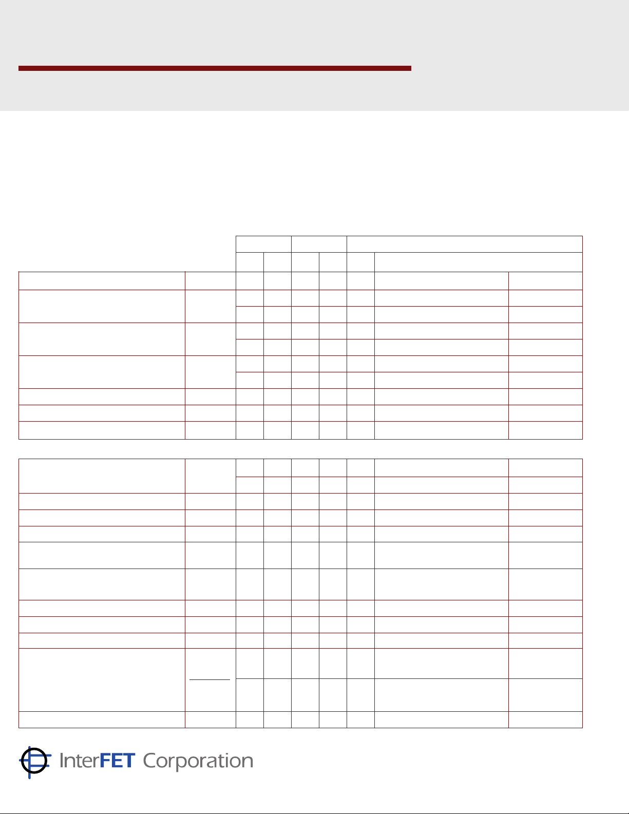
Absolute maximum ratings at TA= 25¡C
Reverse Gate Source & Reverse Gate Drain Voltage – 50 V
Gate Current 50 mA
Total Device Power Dissipation (each side) 250 mW
@ 85°C Case Temperature (both sides) 500 mW
Power Derating (both sides) 4.3 mW/°C
At 25°C free air temperature: 2N3957 2N3958 Process NJ16
Static Electrical Characteristics Min Max Min Max Unit Test Conditions
Gate Source Breakdown Voltage V
(BR)GSS
– 50 – 50 V IG= – 1 µA, VDS= ØV
– 100 – 100 pA VGS= – 30V, VDS= ØV
Gate Reverse Current I
GSS
– 500 – 500 nA VGS= – 30V, VDS= ØV TA= 125°C
– 50 – 50 pA VDS= 20V, ID= 200 µA
Gate Operating Current I
G
– 250 – 250 nA VDS= 20V, ID= 200 µA TA= 125°C
– 4.2 – 4.2 V VDS= 20V, ID= 50 µA
Gate Source Voltage V
Gate Source Cutoff Voltage V
Gate Source Forward Voltage V
Drain Saturation Current (Pulsed) I
GS
GS(OFF)
GS(F)
DSS
– 0.5 – 4 – 0.5 – 4 V VDS= 20V, ID= 200 µA
– 1 – 4.5 – 1 – 4.5 V VDS= 20V, ID= 1 nA
22VV
= Ø, IG= 1 mA
DS
0.5 5 0.5 5 mA VDS= 20V, VGS= ØV
Dynamic Electrical Characteristics
Common Source
Forward Transconductance
Common Source Output Conductance g
Common Source Input Capacitance C
Drain Gate Capacitance C
Common Source
Reverse Transfer Capacitance
g
fs
os
iss
dgo
C
rss
Noise Figure NF 0.5 0.5 dB
Differential Gate Current | IG1– IG2|10 10nAV
Saturation Drain Current Ratio I
Differential Gate Source Voltage | V
Differential Gate Source
Voltage with Temperature
Transconductance Ratio g
DSS1
∆V
fs1
GS1
GS1
∆T
/ g
1000 3000 1000 3000 µS VDS= 20V, VGS= ØV f = 1 kHz
1000 1000 µS VDS= 20V, VGS= ØV f = 200 MHz
35 35 µS VDS= 20V, VGS= ØV f = 1 kHz
44pFV
= 20V, VGS= ØV f = 1 MHz
DS
1.5 1.5 pF VDS= 10V, IS= ØA f = 1 MHz
1.2 1.2 pF VDS= 20V, VGS= ØV f = 1 MHz
VDS= 20V, VGS= ØV
RG= 10MΩ
= 20V, ID= 200 µA TA= 125°C
DS
/ I
– V
– V
0.9 1 0.85 1 VDS= 20V, VGS= ØV
DSS2
| 20 25 mV V
GS2
68mVV
GS2
= 20V, ID= 200 µA
DS
= 20V, ID= 200 µA
DS
7.5 10 mV VDS= 20V, ID= 200 µA
0.9 1 0.85 1 VDS= 20V, ID= 200 µA f = 1 kHz
fs2
TOÐ71 Package
See Section G for Outline Dimensions
1000 N. Shiloh Road, Garland, TX 75042
(972) 487-1287 FAX (972) 276-3375
f = 100 Hz
TA= 25°C
to – 55°C
TA= 25°C
to 125°C
Pin Configuration
1 Source, 2 Drain, 3 Gate, 5 Source,
6 Drain, 7 Gate
www.interfet.com
 Loading...