

IEI Technology WAFER-BT, WAFER-BT-i1-J19001-R10, WAFER-BT-i1-N29301-R10, WAFER-BT-i1-N28071-R10 User Manual
Page 1
WAFER-BT
Page I
WAFER-BT
MODEL:
3.5” S BC with Int e l® 22n m At om™/Ce le ron® on-board SoC,
Rev. 1.0 1 - 4 De ce mbe r, 2014
WAFER-BT CPU Card
VG A/LVDS/iDP, Dual PC Ie G bE , USB 3.0, PCIe Mini,
SATA 3Gb/s, mSATA, COM, Audio and RoHS
User Manual
Page 2

WAFER-BT
Page II
Revis ion
Date Version Changes
4 December, 2014 1.01 Update Section 3.2.23: USB connectors pinouts
7 July, 2014 1.00 Initial release
Page 3

WAFER-BT
Page III
Copyright
COP YRIGHT NOTICE
The information in this document is subject to change without prior notice in order to
improve reliabilit y, design and funct ion and d oes not r epresent a com mitm ent on the part
of the manufacturer.
In no event will the manufacturer be liable for direct, indirect, special, incidental, or
consequential damages arising out of the use or inability to use the product or
documentation, even if advised of the possibility of such damages.
This document contains proprietary information protected by copyright. All rights are
reserved. No part of this manual may be reproduced by any mechanical, e lectronic, or
other means in any form without prior written permission of the manufacturer.
TRADEMARKS
All registered tradem ark s and produc t nam es ment ioned here in are us ed for identif icatio n
purposes only and m ay be trademarks and/or registe red trademarks of their respective
owners.
Page 4

WAFER-BT
Page IV
Table of Contents
1 INTRODUCTION .......................................................................................................... 1
1.1 INTRODUCTION ........................................................................................................... 2
1.2 MODEL VARIATIONS ................................................................................................... 2
1.3 FEATURES ................................................................................................................... 3
1.4 CONNECTORS ............................................................................................................. 4
1.5 DIMENSIONS ............................................................................................................... 5
1.6 DATA FLOW ................................................................................................................ 6
1.7 TECHNICAL SPECIFICATIONS ...................................................................................... 7
2 UNPACKING ............................................................................................................... 10
2.1 ANTI-STATIC PRECAUTIONS ....................................................................................... 11
2.2 UNPACKING PRECAUTIONS ........................................................................................ 11
2.3 PACKING LIST ........................................................................................................... 12
2.4 OPTIONAL ITEMS ...................................................................................................... 13
3 CONNECTORS ........................................................................................................... 14
3.1 PERIPHERAL INTERFACE CONNECTORS ..................................................................... 15
3.1.1 WAFER-BT Layout ........................................................................................... 15
3.1.2 Peripheral Interface Connectors ..................................................................... 15
3.1.3 External Interface Panel Connectors ............................................................... 17
3.2 INTERNAL PERIPHERAL CONNECTORS ...................................................................... 17
3.2.1 +12V DC-IN Power Connector ....................................................................... 17
3.2.2 Audio Connector .............................................................................................. 18
3.2.3 Battery Connector ............................................................................................ 19
3.2.4 Buzzer Connector ............................................................................................. 20
3.2.5 CPU Fan Connector ........................................................................................ 21
3.2.6 DDR3L SO-DIMM Slot .................................................................................... 21
3.2.7 Digital I/O Connector ...................................................................................... 22
3.2.8 Display Port Connector ................................................................................... 23
3.2.9 Front Panel Connector .................................................................................... 24
3.2.10 iRIS-1010 module slot .................................................................................... 25
Page 5

WAFER-BT
Page V
3.2.11 Keyboard and Mouse Connector .................................................................... 25
3.2.12 LVDS Backlight Inverter Connector .............................................................. 26
3.2.13 LVDS LCD Connector ................................................................................... 27
3.2.14 LAN LED Connector ...................................................................................... 28
3.2.15 PCIe Mini Card Slot ...................................................................................... 29
3.2.16 Power Button Connector ................................................................................ 30
3.2.17 Reset Button Connector ................................................................................. 31
3.2.18 RS-232 Serial Port Connectors ...................................................................... 31
3.2.19 RS-422/485 Serial Port Connector ................................................................ 32
3.2.20 SATA 3Gb/s Drive Connector ........................................................................ 33
3.2.21 SATA Power Connector .................................................................................. 34
3.2.22 SMBUS Connector ......................................................................................... 35
3.2.23 USB Connectors ............................................................................................. 35
3.3 EXTERNAL PERIPHERAL INTERFACE CONNECTOR PANEL ......................................... 36
3.3.1 LAN Connector ................................................................................................ 37
3.3.2 USB Connectors ............................................................................................... 38
3.3.3 RS-232 Serial Port Connector ......................................................................... 38
3.3.4 VGA Connector ................................................................................................ 39
4 INSTALLATION ......................................................................................................... 41
4.1 ANTI-STATIC PRECAUTIONS ...................................................................................... 42
4.2 INSTALLATION CONSIDERATIONS .............................................................................. 42
4.3 SO-DIMM INSTALLATION ....................................................................................... 44
4.4 SYSTEM CONFIGURATION ......................................................................................... 45
4.4.1 AT/ATX Mode Select Switch ............................................................................. 45
4.4.2 Clear CMOS Button ......................................................................................... 46
4.4.3 LVDS Panel Resolution Selection .................................................................... 46
4.4.4 LVDS Voltage Selection .................................................................................... 48
4.4.5 Flash Descriptor Security Override Jumper .................................................... 49
4.5 INTERNAL PERIPHERAL DEVICE CONNECTIONS ........................................................ 50
4.5.1 Audio Kit Installation ....................................................................................... 50
4.5.2 SATA Drive Connection ................................................................................... 51
4.5.3 Single RS-232 Cable ........................................................................................ 52
4.6 EXTERNAL PERIPHERAL INTERFACE CONNECTION ................................................... 53
4.6.1 LAN Connection ............................................................................................... 54
Page 6

WAFER-BT
Page VI
4.6.2 Serial Device Connection ................................................................................ 55
4.6.3 USB Connection ............................................................................................... 55
4.6.4 VGA Monitor Connection ................................................................................ 56
5 BIOS .............................................................................................................................. 58
5.1 INTRODUCTION ......................................................................................................... 59
5.1.1 Starting Setup ................................................................................................... 59
5.1.2 Using Setup ...................................................................................................... 59
5.1.3 Getting Help ..................................................................................................... 60
5.1.4 Unable to Reboot after Configuration Changes .............................................. 60
5.1.5 BIOS Menu Bar ................................................................................................ 60
5.2 MAIN ........................................................................................................................ 61
5.3 ADVANCED ............................................................................................................... 62
5.3.1 ACPI Settings ................................................................................................... 63
5.3.2 Super IO Configuration ................................................................................... 64
5.3.2.1 Serial Port n Configuration ....................................................................... 64
5.3.3 Hardware Monitor ........................................................................................... 68
5.3.3.1 Smart Fan Mode Configuration ................................................................ 69
5.3.4 RTC Wake Settings ........................................................................................... 72
5.3.5 Serial Port Console Redirection ...................................................................... 73
5.3.5.1 Console Redirection Settings .................................................................... 74
5.3.6 CPU Configuration .......................................................................................... 77
5.3.7 IDE Configuration ........................................................................................... 78
5.3.8 USB Configuration ........................................................................................... 79
5.4 CHIPSET ................................................................................................................... 80
5.4.1 North Bridge Configuration ............................................................................. 81
5.4.1.1 Intel IGD Configuration ............................................................................ 82
5.4.2 Southbridge Configuration .............................................................................. 83
5.4.2.1 PCI Express Configuration ....................................................................... 85
5.5 SECURITY ................................................................................................................. 86
5.6 BOOT ........................................................................................................................ 87
5.7 EXIT ......................................................................................................................... 89
A BIOS MENU OPTIONS ............................................................................................. 91
B TERMINOLOGY ........................................................................................................ 94
Page 7

WAFER-BT
Page VII
C HAZARDOUS MATERIALS DISCLOSURE ......................................................... 99
C.1 HAZARDOUS MATERIAL DISCLOSURE TABLE FOR IPB PRODUCTS CERTIFIED AS
ROHS COMPLIANT UNDER 2002/95/EC WITHOUT MERCURY ..................................... 100
Page 8

WAFER-BT
Page VIII
List of Figures
Figure 1-1: WAFER-BT ................................................................................................................... 2
Figure 1-2: Connectors
Figure 1-3: Dimensions (mm)
Figure 1-4: Data Flow Diagram
Figure 3-1: Connector and Jumper Locati o n s (Front)
Figure 3-2: +12V DC-IN Power Connector Location
Figure 3-3: Audio Connector Location
Figure 3-4: Battery Connector Location
Figure 3-5: Buzzer Connector Location
Figure 3-6: CPU Fan Connector Locations
Figure 3-7: DDR3L SO-DIMM Slot Location
Figure 3-8: Digital I/O Connector Location
Figure 3-9: Display Port Connector Location
Figure 3-10: Front Panel Connector Location
Figure 3-11: iRIS-1010 Module Slot Location
Figure 3-12: Keyboard and Mouse Location
Figure 3-13: Backlight Inverter Connector Location
Figure 3-14: LVDS Connector Location
.................................................................................................................. 4
........................................................................................................ 5
...................................................................................................... 6
..............................................................15
..................................................................18
.......................................................................................19
.....................................................................................20
.....................................................................................20
................................................................................21
...............................................................................22
................................................................................22
............................................................................23
...........................................................................24
............................................................................25
..............................................................................26
.................................................................27
......................................................................................28
Figure 3-15: LAN LED Connector Location
Figure 3-16: PCIe Mini Card Slot Location
Figure 3-17: Power Button Connector Location
Figure 3-18: Reset Button Connector Locati o n
Figure 3-19: RS-232 Serial Port Connectors Locations ............................................................32
Figure 3-20: RS-422/485 Connector Location
Figure 3-21: SATA 3Gb/s Drive Connectors Locations
Figure 3-22: SATA Power Connector Locatio n
Figure 3-23: SMBUS Connectors Location
Figure 3-24: USB Connectors Locations
Figure 3-25: External Peripheral Interface Connector
Figure 3-26: LAN Connector
Figure 3-27: RS-232 Serial Port Connector
...............................................................................29
.................................................................................30
........................................................................30
.........................................................................31
............................................................................33
............................................................34
.........................................................................34
................................................................................35
....................................................................................36
..............................................................37
........................................................................................................37
................................................................................39
Page 9

WAFER-BT
Page IX
Figure 3-28: VGA Connector .......................................................................................................39
Figure 4-1: SO-DIMM Installation
Figure 4-2: AT/ATX Mode Select Switch Location
Figure 4-3: Clear CMOS Button Location
Figure 4-4: LVDS Panel Resolution Sele ction Switch Location
Figure 4-5: LVDS Voltage Selection Jumper Location
Figure 4-6: Flash Descriptor Security Override Jumper Location
Figure 4-7: Audio Kit Cable Connection
Figure 4-8: SATA Drive Cable Connection
Figure 4-9: Single RS-232 Cable Installation
Figure 4-10: LAN Connection
Figure 4-11: Serial Device Connector
Figure 4-12: USB Connector
Figure 4-13: VGA Connector
................................................................................................44
....................................................................46
...................................................................................46
..............................................48
.............................................................49
..........................................50
.....................................................................................51
.................................................................................52
.............................................................................53
......................................................................................................54
.........................................................................................55
........................................................................................................56
.......................................................................................................57
Page 10

WAFER-BT
Page X
List of Tables
Table 1-1: WAFER-BT Model Variations ....................................................................................... 2
Table 1-2: Technical Specifications
Table 3-1: Peripheral Interface Connectors
Table 3-2: Rear Panel Connectors
Table 3-3: +12V DC-IN Power Connector Pinouts
Table 3-4: Audio Connector Pinouts
Table 3-5: Battery Connector Pinouts
Table 3-6: Buzzer Connector Pinouts
Table 3-7: CPU Fan Connector Pinouts
Table 3-8: Digital I/O Connector Pinouts
Table 3-9: Display Port Connector Pinouts
Table 3-10: Front Panel Connector Pinouts
Table 3-11: Keyboard and Mouse Connector Pinouts
Table 3-12: Backlight Inverter Connector Pinouts
Table 3-13: LVDS Connector Pinouts
Table 3-14: LAN LED Connector Pinouts
Table 3-15: Power Button Connector Pinouts
Table 3-16: Reset Button Connector Pinouts
.............................................................................................. 9
...............................................................................16
..............................................................................................17
.....................................................................18
..........................................................................................19
........................................................................................20
.........................................................................................21
.....................................................................................21
....................................................................................23
...............................................................................24
...............................................................................25
..............................................................26
....................................................................27
.........................................................................................28
...................................................................................29
...........................................................................31
............................................................................31
Table 3-17: RS-232 Serial Port Connector Pinouts
Table 3-18: RS-422/485 Connector Pinouts
Table 3-19: DB-9 RS-42 2/ 485 Pin out s
Table 3-20: SATA Power Connector Pinouts
Table 3-21: SMBUS Connectors Pinouts ...................................................................................35
Table 3-22: USB Connector Pinouts
Table 3-23: LAN Pinouts
Table 3-24: Connector LEDs
Table 3-25: USB 2.0 Port Pinouts
Table 3-26: USB 3.0 Port Pinouts
Table 3-27: RS-232 Se ria l Por t Connector Pinouts
Table 3-28: VGA Connector Pinouts
Table 4-1: AT/ATX Mode Select Switch Settings
...................................................................32
...............................................................................33
.........................................................................................33
.............................................................................35
...........................................................................................36
..............................................................................................................37
........................................................................................................38
................................................................................................38
................................................................................................38
...................................................................39
...........................................................................................40
.......................................................................45
Page 11

WAFER-BT
Page XI
Table 4-2: Clear CMOS Button Settings .....................................................................................46
Table 4-3: LVDS Panel Resolution Selection
Table 4-4: LVDS Voltage Selection Jumper Settings
Table 4-5: Flash Descriptor Security Override Jumper Setting s
Table 5-1: BIOS Navigation Keys
.............................................................................47
................................................................48
.............................................49
................................................................................................60
Page 12

WAFER-BT
Page XII
List of BIOS Menus
BIOS Menu 1: Main .......................................................................................................................61
BIOS Menu 2: Advanced
BIOS Menu 3: ACPI Configuration
BIOS Menu 4: Super IO Configuration
BIOS Menu 5: Serial Port n Configuration Menu
BIOS Menu 6: Hardware Monitor
BIOS Menu 7: Smart Fan Mode Configuration
BIOS Menu 8: RTC Wake Settings
BIOS Menu 9: Serial Port Console Redirection
BIOS Menu 10: Console Redirection Settings
BIOS Menu 11: CPU Configuration
BIOS Menu 12: IDE
BIOS Menu 13: USB Configuration
BIOS Menu 14: Chipset
BIOS Menu 15: Northbridge Chipset Configuration
BIOS Menu 16: Integrated Graphics
BIOS Menu 17: Southbridge Chipset Configuration
BIOS Menu 18: Console Redirection Settings
Configuration ...............................................................................................78
..............................................................................................................62
..............................................................................................63
........................................................................................64
.......................................................................64
.................................................................................................69
..........................................................................70
..............................................................................................72
.........................................................................74
...........................................................................75
.............................................................................................77
.............................................................................................79
................................................................................................................81
..................................................................81
...........................................................................................82
.................................................................84
...........................................................................85
BIOS Menu 19: Security
BIOS Menu 20: Boot
BIOS Menu 21:Exit
...............................................................................................................86
.....................................................................................................................87
........................................................................................................................89
Page 13

WAFER-BT
Page 1
Chapter
1
1 Introduction
Page 14

WAFER-BT
Page 2
1.1 Introduction
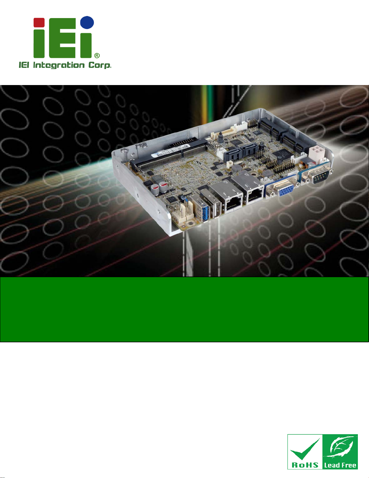
Figure 1-1: WAFER-BT
The WAFER-BT SBC m otherboard is an Intel® Atom™/Celeron® processor platform. It
supports one 204-pin 1066/1333 MH z single-channel DDR3L SO-DIMM supports up to
8GB (J1900, N2930, E3845, E3827, E3826) or 4GB (N2807, E3825, E3815).
The WAFER-BT includes a VGA connector, a LVDS connector and an iDP connector.
Expansion and I/O include one USB 2.0 connector and one USB 3.0 connector on the rear
panel, four USB 2.0 connectors by pin header and two SATA 3Gb/s co nnectors. Serial
device connectivit y is provided by two internal RS-232 connectors, one external RS-232
connector and one internal RS-422/485 connector. Two RJ-45 Ethernet connectors
provide the system with smooth connections to an external LAN.
1.2 Model Variations
The model variations of the WAFER-BT Series are listed below.
Model No. SoC
WAFER-BT-i1-J19001-R10
WAFER-BT-i1-N29301-R10
Intel® Celeron® quad-core J1900 (10W)
Intel® Celeron® quad-core N2930 (7.5W)
WAFER-BT-i1-N28071-R10
WAFER-BT-i1-E38XX1-R10
Table 1-1: WAFER-BT Model Variations
Intel® Celeron® dual-core N2807 (4.3W)
Intel® Atom™ E38XX
Page 15

WAFER-BT
Page 3
1.3 Features
Some of the WAFER-BT motherboard features are listed below:
3.5" SBC supports Intel® 22nm Atom™/Celeron® on-board SoC
Dual independent display support
One 204-pin 1066/1333 MHz single-channel DDR3L SO-DIMM supports up to
COM, USB 3.0, SATA 3Gb/s, PCIE mini, mSATA and Audio support
IEI one key recovery solution allows you to create rapid OS backup and
8GB (J1900, N2930, E3845, E3827, E3826) or 4GB (N2807, E3825, E3815)
recovery
Page 16
WAFER-BT
Page 4
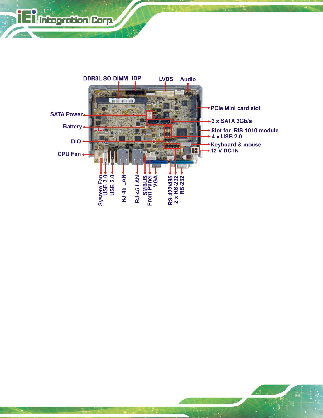
1.4 Connectors
The connectors on the WAFER-BT are shown in the figure below.
Figure 1-2: Connectors
Page 17
WAFER-BT
Page 5
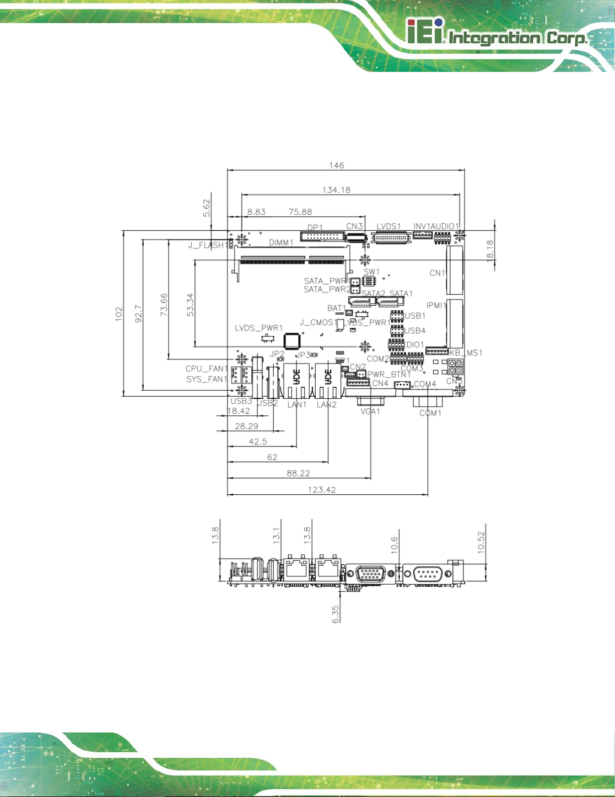
1.5 Dimensions
The dimensions of the board are listed below:
Figure 1-3: Dimensions (mm)
Page 18
WAFER-BT
Page 6
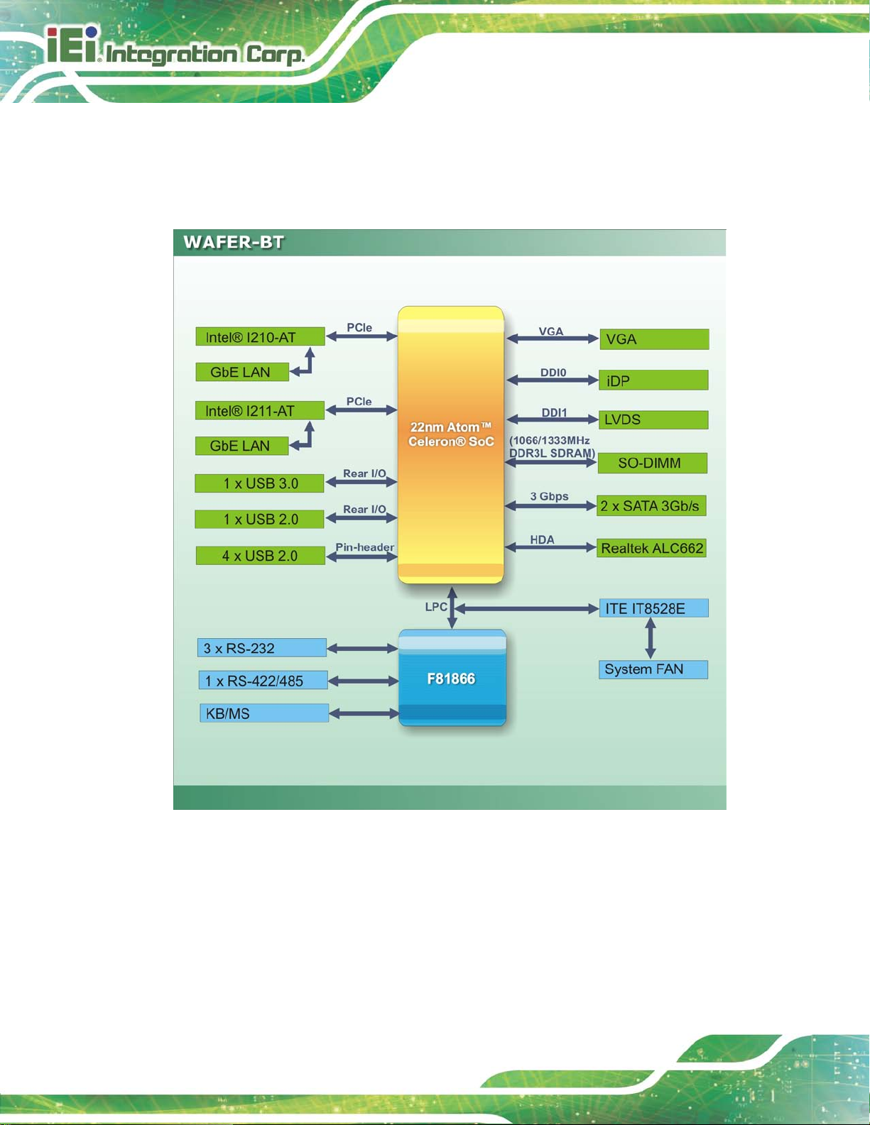
1.6 Data Flow
Figure 1-4 shows the data flow between the system chipset, the CPU and other
components installed on the motherboard.
Figure 1-4: Data Flow Diagram
Page 19
WAFER-BT
Page 7
1.7 Technical Specifications
WAFER-BT technical specifications are listed belo w.
Specification WAFER-BT
SoC
Intel® Atom™ E3845 on-board SoC (1.91GHz, quad-core,
2MB cache, TDP=10W)
Intel® Atom™ E3827 on-board SoC (1.75GHz, dual-core,
1MB cache, TDP=8W)
Intel® Atom™ E3826 on-board SoC (1.46GHz, dual-core,
1MB cache, TDP=7W)
Intel® Atom™ E3825 on-board SoC (1.33GHz, dual-core,
1MB cache, TDP=6W)
Intel® Atom™ E3815 on-board SoC (1.46GHz, single-core,
512KB cache, TDP=5W)
Intel® Celeron® J1900 on-board SoC (2GHz, quad-core,
2MB cache, TDP=10W)
Intel® Celeron® N2930 on-board SoC (1.83GHz, quad-core,
2MB cache, TDP=7.5W)
Intel® Celeron® N2807 on-board SoC (1.58GHz, dual-core,
2MB cache, TDP=4.3W)
BIOS
Mem o ry
Graphics
Displa y Output
AMI UEFI BIOS
One 204-pin 1066/1333 MHz single-channel DDR3L
SO-DIMM supports up to 8GB (J1900, N2930, E3845, E3827,
E3826) or 4GB (N2807, E3825, E3815)
Intel® HD Graphics Gen 7 Engines with 4 execution unit,
supports DX11.1, OpenGL 4.2 and OpenCL1.2
Dual Independent Display
1 x VGA (Resolution: 2560x1600@60Hz)
1 x 24-bit dual-channel LVDS connector (1920x1200@60Hz)
1 x iDP interface for HDMI, LVDS, VGA, DVI, DP (up to
3840x2160@60 Hz)
Page 20
WAFER-BT
Page 8
Specification WAFER-BT
Ethernet
Super IO
Embedded Controller
Audio
Watchdog Timer
I/O Inte rfa c e
Audio Connector
Ethernet
KB/MS
Serial P orts
USB Ports
1 x PCIe GbE by Intel I210 controller (LAN1)
1 x PCIe GbE by Intel I21 1 controller (LAN2)
Fintek F81866
ITE IT8528E
Realtek ALC662 HD codec
Software programmable support 1~255 sec. system reset
1 x Analog audio by 10-pin (2x5) header
Two RJ-45 ports
1 x PS/2 KB/MS
1 x RS-422/485 (by pin header)
3 x RS-232 (1 on rear I/O, 2 by pin header)
1 x USB 3.0 (on rear I/O)
5 x USB 2.0 (1 on rear I/O, 4 by pin header)
Front Panel
LAN LED
FAN
SMBus
Expansion
iRIS Remote Management
Module
Digital I/O
Storage
1 x 6-pin (1x6) wafer for power LED & HDD LED
1 x 2-pin (1x2) wafer for power button
1 x 2-pin (1x2) wafer for power reset button
2 x 2-pin header for LAN1 Link LED, LAN2 Link LED
1 x 4-pin CPU fan connector
1 x 4-pin system fan connector
1 x 4-pin (1x4) wafer
1 x Full-size PCIe Mini card slot with mSATA support (SATA2
and mSATA share SATA signal)
1 x iRIS-1010 slot
8-bit digital I/O (4-bit input, 4-bit output)
Page 21
WAFER-BT
Page 9
Specification WAFER-BT
S erial ATA
Environmental and Power Specifications
Power Supply
Power Consumption
Operating Temperature
Storage Temperature
Humidity
Physical Spe cifications
Dimensions 146mm x 102mm
Weight GW/NW
Table 1-2: Technical Specifications
2 x SATA 3Gb/s with 5V SATA power connector (no RAID)
12V DC input only (AT/ATX support)
+12V@1.45A (Intel® Celeron® J1900 CPU, 1 x 8GB 1333
MHz DDR3 memory)
-20°C ~ 60°C
-30°C ~ 70°C
5% ~ 95%, non-condensing
600 g / 250 g
Page 22

WAFER-BT
Page 10
Chapter
2
2 Unpacking
Page 23
WAFER-BT
Page 11
2.1 Anti-s tatic Precautions
WARNING!
Static electricity can destroy certain electronics. Make sure to follow the
ESD precautions to preve nt damage to the product, and injur y to the
user.
Make sure to adhere to the following guidelines:
Wear an anti-static wristband: Wearing an anti-static wrist ban d can prev ent
electrostatic discharge.
Self-grounding: Touch a grounded conductor every few minutes to discharge
any excess static buildup.
Use an anti-static pad: When configuring any circuit board, place it on an
anti-static mat.
Only handle the edges of the PCB: Don't touch the surface of the
motherboard. Hold the motherboard by the edges when handling.
2.2 Unpacking Precautions
When the WAFER-BT is unpacked, please do the following:
Follow the antistatic guidelines above.
Make sure the packing box is facing upwards when opening.
Make sure all the packing list items are present.
Page 24
WAFER-BT
Page 12
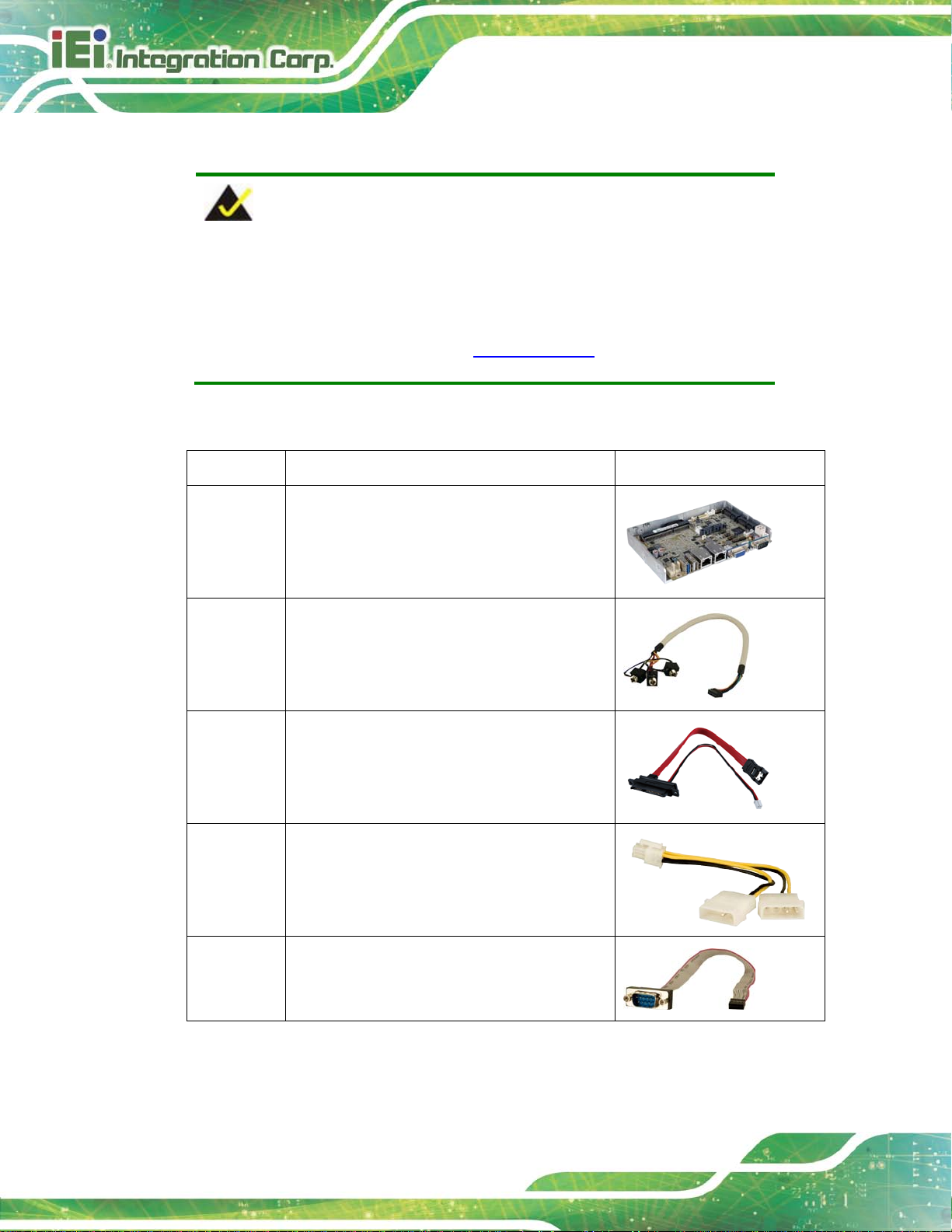
2.3 Pack i ng List
NOTE:
If any of the components listed in the checklist below are missing, do not
proceed with the installation. Contact the IEI reseller or vendor the
WAFER-BT was purchased from or contact an IEI sales representative
directly by sending an email to
The WAFER-BT is shipped with the following components:
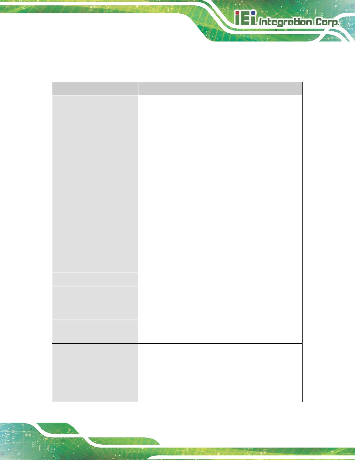
Quantity Item and Part Number Image
1 1 x WAFER-BT single board computer with
specific heat sink
1 Audio cable
(P/N: 32000-072100-RS)
1 SATA with 5V output cable kit
(P/N: 32801-000201-100-RS)
sales@iei.com.tw.
1 Power cable
(P/N: 32100-087100-RS)
1 RS-232 cable
(P/N: 32205-002700-100-RS)
 Loading...