

Page 1

WAFER-AL SBC
Page I
WAFER-AL
MODEL:
3.5” SBC with 14nm Intel® Pentium®/Celeron® On-board SoC,
Rev. 1.01 - May 3, 2018
WAFER-AL CPU Card
DP++, VGA, LVDS, Dual PCIe GbE, USB 3.0, PCIe Mini, mSATA,
SATA 6Gb/s, RS-232/422/485, HD Audio, SIM Slot and RoHS
User Manual
Page 2
WAFER-AL SBC
Page II
Date Version Changes
May 3, 2018 1.01 Deleted E series SKUs
Updated Chapter 6: Software Drivers
November 30, 2017 1.00 Initial release
Revision
Page 3

WAFER-AL SBC
Page III
Copyright
COPYRIGHT NOTICE
The information in this document is subject to change without prior notice in order to
improve reliability, design and function and does not represent a commitment on the part
of the manufacturer.
In no event will the manufacturer be liable for direct, indirect, special, incidental, or
consequential damages arising out of the use or inability to use the product or
documentation, even if advised of the possibil ity of such damages.
This document contains proprietary information protected by copyright. All rights are
reserved. No part of this manual may be reproduced by any mechanical, electronic, or
other means in any form without prior written permission of the manufacturer.
TRADEMARKS
All registered trademarks and product names mentioned herein are used for identification
purposes only and may be trademarks and/or registered trademarks of their respective
owners.
Page 4
WAFER-AL SBC
Page IV
Manual Conventions
WARNING
Warnings appear where overlooked details may cause damage to t he
equipment or result in personal injury. Warnings should be t aken
seriously.
CAUTION
Cautionary messages should be heeded to help red uce the chance of
losing data or damaging the product.
NOTE
These messages inform the reader of essent ial but non-critical
information. These messages should be read carefully as any directions
or instructions contained therein ca n help avoid making mistakes.
HOT SURFACE
This symbol indicates a hot surface that shoul d not be touched without
taking care.
Page 5

WAFER-AL SBC
Page V
Table of Contents
1 INTRODUCTION .......................................................................................................... 1
1.1 INTRODUCTION ........................................................................................................... 2
1.2 MODEL VARIATIONS ................................................................................................... 3
1.3 FEATURES ................................................................................................................... 3
1.4 CONNECTORS ............................................................................................................. 4
1.5 DIMENSIONS ............................................................................................................... 6
1.6 DATA FLOW ................................................................................................................ 7
1.7 TECHNICAL SPECIFICATIONS ...................................................................................... 8
2 UNPACKING ............................................................................................................... 10
2.1 ANTI-STATIC PRECAUTIONS ....................................................................................... 11
2.2 UNPACKING PRECAUTIONS ........................................................................................ 11
2.3 PACKING LIST ........................................................................................................... 12
2.4 OPTIONAL ITEMS ...................................................................................................... 13
3 CONNECTORS ........................................................................................................... 14
3.1 PERIPHERAL INTERFACE CONNECTORS ..................................................................... 15
3.1.1 W AFER-AL Layout ........................................................................................... 15
3.1.2 Peripheral Interface Connectors ..................................................................... 16
3.1.3 External Interface Panel Connectors ............................................................... 17
3.2 INTERNAL PERIPHERAL CONNECTORS ...................................................................... 18
3.2.1 +12V DC-IN Power Connector ....................................................................... 18
3.2.2 Audio Connector .............................................................................................. 19
3.2.3 Battery Connector ............................................................................................ 20
3.2.4 Digital I/O Connector ...................................................................................... 21
3.2.5 Fan Connector ................................................................................................. 22
3.2.6 iDP Connector (Optional) ............................................................................... 23
3.2.7 LVDS Backlight Inverter Connector ................................................................ 24
3.2.8 LVDS LCD Connector ..................................................................................... 25
3.2.9 LAN LED Connectors ...................................................................................... 26
3.2.10 mSATA Module Slot ........................................................................................ 27
Page 6

WAFER-AL SBC
Page VI
3.2.11 PCIe Mini Card Slot ....................................................................................... 29
3.2.12 Power and HDD LED Connector .................................................................. 31
3.2.13 Power Button Connector ................................................................................ 32
3.2.14 Reset Button Connector ................................................................................. 33
3.2.15 RS-232 Serial Port Connectors ...................................................................... 34
3.2.16 RS-232/422/485 Serial Port Connectors ....................................................... 35
3.2.17 SATA 6Gb/s Connectors ................................................................................. 36
3.2.18 SATA Power Connectors ................................................................................ 37
3.2.19 SIM Card Slot ................................................................................................. 38
3.2.20 SMBus/I2C Connector .................................................................................... 38
3.2.21 SPI Flash Connector ...................................................................................... 39
3.2.22 TPM Connector .............................................................................................. 40
3.2.23 USB 2.0 Connectors ....................................................................................... 41
3.3 EXTERNAL PERIPHERAL INTERFACE CONNECTOR PANEL ......................................... 42
3.3.1 DisplayPort++ Connector ............................................................................... 42
3.3.2 LAN Connectors ............................................................................................... 44
3.3.3 USB Connectors ............................................................................................... 44
3.3.4 VGA Connector ................................................................................................ 45
4 INSTALLATION ......................................................................................................... 47
4.1 ANTI-STATIC PRECAUTIONS ...................................................................................... 48
4.2 INSTALLATION CONSIDERATIONS .............................................................................. 48
4.3 SO-DIMM INSTALLATION ....................................................................................... 50
4.4 MSATA MODULE INSTALLATION .............................................................................. 50
4.4.1 Full-size mSATA Module Installation .............................................................. 51
4.4.2 Half-size mSATA Module Installation .............................................................. 52
4.5 PCIE MINI CARD INSTALLATION .............................................................................. 55
4.6 SIM CARD INSTALLATION ........................................................................................ 55
4.7 SYSTEM CONFIGURATION ......................................................................................... 57
4.7.1 AT/A TX Mode Select Switch ............................................................................. 57
4.7.2 Clear CMOS Button ......................................................................................... 58
4.7.3 LVDS Voltage Select Jumper ............................................................................ 59
4.7.4 LVDS Backlight Mode Select Jumper .............................................................. 60
4.7.5 LVDS Panel Resolution Select Switch ............................................................. 61
4.7.6 RS-232/422/485 Mode Select Switch ............................................................... 62
Page 7

WAFER-AL SBC
Page VII
4.8 CHASSIS INSTALLATION ............................................................................................ 63
4.8.1 Airflow .............................................................................................................. 63
4.8.2 Motherboard Installation ................................................................................. 63
4.9 INTERNAL PERIPHERAL DEVICE CONNECTIONS ........................................................ 63
4.9.1 Audio Kit Installation ....................................................................................... 63
4.9.2 AT Power Connection ...................................................................................... 64
4.9.3 SATA Drive Connection ................................................................................... 66
5 BIOS .............................................................................................................................. 68
5.1 INTRODUCTION ......................................................................................................... 69
5.1.1 Starting Setup ................................................................................................... 69
5.1.2 Using Setup ...................................................................................................... 69
5.1.3 Getting Help ..................................................................................................... 70
5.1.4 Unable to Reboot after Configuration Changes .............................................. 70
5.1.5 BIOS Menu Bar ................................................................................................ 70
5.2 MAIN ........................................................................................................................ 71
5.3 ADVANCED ............................................................................................................... 72
5.3.1 T rusted Computing ........................................................................................... 73
5.3.2 ACPI Settings ................................................................................................... 74
5.3.3 F81866 Super IO Configuration ...................................................................... 75
5.3.3.1 Serial Port n Configuration ....................................................................... 75
5.3.3.1.1 Serial Port 1 Configuration ................................................................ 76
5.3.3.1.2 Serial Port 2 Configuration ................................................................ 77
5.3.3.1.3 Serial Port 3 Configuration ................................................................ 78
5.3.3.1.4 Serial Port 4 Configuration ................................................................ 79
5.3.4 F81866 H/W Monitor ....................................................................................... 80
5.3.4.1 Smart Fan Mode Configuration ................................................................ 81
5.3.5 USB Configuration ........................................................................................... 82
5.3.6 CPU Configuration .......................................................................................... 84
5.3.7 RTC Wake Settings ........................................................................................... 86
5.3.8 Power Saving Configuration ............................................................................ 87
5.3.9 Serial Port Console Redirection ...................................................................... 88
5.3.9.1 Legacy Console Redirection Settings ....................................................... 89
5.3.10 IEI Feature ..................................................................................................... 90
5.4 CHIPSET ................................................................................................................... 91
Page 8

WAFER-AL SBC
Page VIII
5.4.1 North Bridge Configuration ............................................................................. 92
5.4.1.1 Intel IGD Configuration ............................................................................ 92
5.4.2 South Bridge Configuration ............................................................................. 94
5.4.2.1 HD-Audio Configuration .......................................................................... 96
5.4.2.2 PCI Express Configuration ....................................................................... 97
5.4.2.2.1 Onboard LAN .................................................................................... 98
5.4.2.2.2 MINI-PCIE ........................................................................................ 99
5.4.2.3 SATA Configuration ................................................................................ 100
5.5 SECURITY ............................................................................................................... 101
5.6 BOOT ...................................................................................................................... 102
5.7 SAVE & EXIT .......................................................................................................... 104
6 SOFTWARE DRIVERS ............................................................................................ 106
6.1 AVAILABLE DRIVERS .............................................................................................. 107
6.2 DRIVER DOWNLOAD .............................................................................................. 108
A REGULATORY COMPLIANCE ............................................................................. 110
B PRODUCT DISPOSAL ............................................................................................. 112
C BIOS MENU OPTIONS ............................................................................................ 114
D DIGITAL I/O INTERFACE ...................................................................................... 117
E WA TCHDOG TIMER ............................................................................................... 120
F HAZARDOUS MATERIALS DISCLOS U RE ........................................................ 123
Page 9

WAFER-AL SBC
Page IX
List of Figures
Figure 1-1: WAFER-AL ................................................................................................................... 2
Figure 1-2: Connectors (Front Side) ............................................................................................. 4
Figure 1-3: Connectors (Solder Side) ........................................................................................... 5
Figure 1-4: Dimensions with Heatsink (mm) ................................................................................ 6
Figure 1-5: Data Flow Diagram ...................................................................................................... 7
Figure 3-1: Connector and Jumper Locations (Front Side) ..................................................... 15
Figure 3-2: Connector and Jumper Locations (Solder Side) ................................................... 15
Figure 3-3: +12V DC-IN Power Connector Location .................................................................. 18
Figure 3-4: Audio Connector Location ....................................................................................... 19
Figure 3-5: Battery Connector Location ..................................................................................... 20
Figure 3-6: Digital I/O Connector Location ................................................................................ 21
Figure 3-7: Fan Connector Location ........................................................................................... 22
Figure 3-8: iDP Connector Location ........................................................................................... 23
Figure 3-9: Backlight Inverter Connector Location ................................................................... 24
Figure 3-10: LVDS Connector Location...................................................................................... 25
Figure 3-11: LAN LED Connector Locations ............................................................................. 26
Figure 3-12: mSATA Module Slot Location ................................................................................ 28
Figure 3-13: PCIe Mini Card Slot Location ................................................................................. 29
Figure 3-14: Power and HDD LED Connector Location ............................................................ 31
Figure 3-15: Power Button Connector Location ........................................................................ 32
Figure 3-16: Reset Button Connector Location ......................................................................... 33
Figure 3-17: RS-232 Serial Port Connector Locations .............................................................. 34
Figure 3-18: RS-232/422/485 Connector Locations ................................................................... 35
Figure 3-19: SATA 6Gb/s Connector Locations ........................................................................ 36
Figure 3-20: SATA Power Connector Locations ....................................................................... 37
Figure 3-21: SIM Card Slot Location ........................................................................................... 38
Figure 3-22: SMBus/I2C Connector Location ............................................................................. 38
Figure 3-23: SPI Flash Connector Location ............................................................................... 39
Figure 3-24: TPM Connector Location ........................................................................................ 40
Figure 3-25: USB Connector Locations...................................................................................... 41
Figure 3-26: External Peripheral Interface Conn ector .............................................................. 42
Page 10

WAFER-AL SBC
Page X
Figure 3-27: HDMI Connector Pinout Locations ........................................................................ 43
Figure 3-28: LAN Connector ........................................................................................................ 44
Figure 3-29: USB 3.0 Port Pinout Locations .............................................................................. 45
Figure 3-30: VGA Connector ....................................................................................................... 46
Figure 4-1: SO-DIMM Installation ................................................................................................ 50
Figure 4-2: Removing the Retention Screw ............................................................................... 51
Figure 4-3: Inserting the Full-size mSATA Module into the Slot at an Angle ......................... 51
Figure 4-4: Securing the mSATA Module ................................................................................... 52
Figure 4-5: Removing the Retention Screw and the Standoff ................................................. 53
Figure 4-6: Installing the Standoff .............................................................................................. 53
Figure 4-7: Inserting the Half-size mSATA Module into the Slot at an A ngle ......................... 54
Figure 4-8: Securing the Half-size mSATA Module ................................................................... 54
Figure 4-9: Unlock SIM Card Slot Cover .................................................................................... 55
Figure 4-10: SIM Card Installation ............................................................................................... 56
Figure 4-11: Lock SIM Card Slot Cover ...................................................................................... 56
Figure 4-12: AT/ATX Mode Select Switch Location .................................................................. 57
Figure 4-13: Clear CMOS Button Location ................................................................................. 58
Figure 4-14: LVDS Voltage Select Jumper Locati o n ................................................................. 59
Figure 4-15: LVDS Backlight Mode Select Jumper Location ................................................... 60
Figure 4-16: LVDS Panel Resolution Select Switch Location .................................................. 61
Figure 4-17: RS-232/422/485 Mode Select Switch Location ..................................................... 62
Figure 4-18: Audio Kit Cable Connection .................................................................................. 64
Figure 4-19: Power Cable to Motherboard Connection ............................................................ 65
Figure 4-20: Connect Power Cable to Power Supply ................................................................ 65
Figure 4-21: SATA Drive Cable Connection ............................................................................... 67
Figure 6-1: IEI Resource Download Center ..............................................................................107
Page 11

WAFER-AL SBC
Page XI
List of Tables
Table 1-1: WAFER-AL Model Variations ....................................................................................... 3
Table 1-2: Technical Specifications .............................................................................................. 9
Table 3-1: Peripheral Interface Connectors ............................................................................... 17
Table 3-2: Rear Panel Connectors .............................................................................................. 17
Table 3-3: +12V DC-IN Power Connector Pinouts ..................................................................... 18
Table 3-4: Audio Connector Pinouts .......................................................................................... 19
Table 3-5: Battery Connector Pinouts ........................................................................................ 21
Table 3-6: Digital I/O Connector Pinouts .................................................................................... 21
Table 3-7: Fan Connector Pinouts .............................................................................................. 22
Table 3-8: iDP Connector Pinouts ............................................................................................... 23
Table 3-9: Backlight Inverter Connector Pinouts ...................................................................... 24
Table 3-10: LVDS Connector Pinouts ......................................................................................... 26
Table 3-11: LAN1 LED Connector (JLAN_LED1) Pinouts ......................................................... 27
Table 3-12: LAN2 LED Connector (JLAN_LED2) Pinouts ......................................................... 27
Table 3-13: mSATA Module Slot Pinouts ................................................................................... 29
Table 3-14: PCIe Mini Card Slot Pinouts .................................................................................... 30
Table 3-15: Power and HDD LED Connector Pinouts ............................................................... 31
Table 3-16: Power Button Connector Pinouts ........................................................................... 32
Table 3-17: Reset Button Connector Pinouts ............................................................................ 33
Table 3-18: RS-232 Serial Port Connector Pinouts ................................................................... 34
Table 3-19: RS-232/422/485 Connector Pinouts ........................................................................ 35
Table 3-20: RS-232/422/485 Cable Pinouts ................................................................................ 36
Table 3-21: SATA Power Connector Pinouts ............................................................................. 37
Table 3-22: SMBus/I2C Connector Pinouts ................................................................................ 39
Table 3-23: SPI Flash Connector Pinouts .................................................................................. 39
Table 3-24: TPM Connector Pinouts ........................................................................................... 40
Table 3-25: USB Connector Pinouts ........................................................................................... 41
Table 3-26: HDMI Connector Pinouts ......................................................................................... 43
Table 3-27: LAN Pinouts .............................................................................................................. 44
Table 3-28: USB 3.0 Port Pinouts ................................................................................................ 45
Table 3-29: VGA Connector Pinouts ........................................................................................... 46
Page 12

WAFER-AL SBC
Page XII
Table 4-1: AT/ATX Mode Select Switch Settings ....................................................................... 57
Table 4-2: LVDS Voltage Select Jumper Settings ..................................................................... 59
Table 4-3: LVDS Backlight Mode Select Jumper S etti n gs........................................................ 60
Table 4-4: LVDS Panel Resolution Selection ............................................................................. 61
Table 4-5: RS-232/422/485 Mode Selection ................................................................................ 62
Table 5-1: BIOS Navigation Keys ................................................................................................ 70
Page 13

WAFER-AL SBC
Page XIII
List of BIOS Menus
BIOS Menu 1: Main ....................................................................................................................... 71
BIOS Menu 2: Advanced .............................................................................................................. 72
BIOS Menu 3: Trusted Computing .............................................................................................. 73
BIOS Menu 4: ACPI Settings ....................................................................................................... 74
BIOS Menu 5: F81866 Super IO Configuration .......................................................................... 75
BIOS Menu 6: Serial Port n Configuration ................................................................................. 75
BIOS Menu 7: F81866 H/W Monitor ............................................................................................. 80
BIOS Menu 8: Smart Fan Mode Configuration .......................................................................... 81
BIOS Menu 9: USB Configuration ............................................................................................... 82
BIOS Menu 10: CPU Configuration ............................................................................................. 84
BIOS Menu 11: RTC Wake Settings ............................................................................................ 86
BIOS Menu 12: Power Saving Configuration ............................................................................. 87
BIOS Menu 13: Serial Port Console Redirection ....................................................................... 88
BIOS Menu 14: Legacy Console Redirection Settings ............................................................. 89
BIOS Menu 15: IEI Feature ........................................................................................................... 90
BIOS Menu 16: Chipset ................................................................................................................ 91
BIOS Menu 17: North Bridge Configuration .............................................................................. 92
BIOS Menu 18: Intel IGD Configuration ...................................................................................... 93
BIOS Menu 19: South Bridge Configuration .............................................................................. 95
BIOS Menu 20: HD-Audio Configuration .................................................................................... 96
BIOS Menu 21: PCI Express Configuration ............................................................................... 97
BIOS Menu 22: Onboard LAN ...................................................................................................... 98
BIOS Menu 23: MINI-PCIE ............................................................................................................ 99
BIOS Menu 24: SATA Configuration .........................................................................................100
BIOS Menu 25: Security .............................................................................................................101
BIOS Menu 26: Boot ...................................................................................................................102
BIOS Menu 27: Save & Exit ........................................................................................................104
Page 14

Page 15

WAFER-AL SBC
Page 1
Chapter
1
1 Introduction
Page 16

WAFER-AL SBC
Page 2
1.1 Introduction
Figure 1-1: WAFER-AL
The WAFER-AL series is a 3.5” single bard computer. It has an on-board 14nm Intel
Pentium
single-channel DDR3 Low Voltage (DDR3L) SDRAM SO-DIMM slot with up to 8.0 GB of
memory.
The WAFER-AL series includes one DP++ connector, one VGA connector and one
18-/24-bit LVDS connector for triple independent display. Two RJ-45 GbE connectors
provide the system with smooth connections to an external LAN.
Expansion and I/O include one PCIe Mini slot supporting mSATA modules, one PCIe Mini
slot with SIM card holder, two USB 3.0 connectors on the rear panel, four USB 2.0
connectors by pin header and two SATA 6Gb/s connectors. Serial device connectivity is
provided by two internal RS-232 connectors and two internal RS-232/422/485 connectors.
®
or Celeron® processor, and supports one 204-pin 1867/1600 MHz
®
Page 17
WAFER-AL SBC
Page 3
1.2 Model Variations
The model variations of the WAFER-AL series are listed below.
Model No. SoC Display Interface
WAFER-AL-N2
WAFER-AL-N1
WAFER-AL-N2-iDP*
WAFER-AL-N1-iDP*
*By order production, MOQ 100
®
Intel
Pentium® N4200 on-board SoC
(up to 2.5 GHz, quad-core, TDP=6 W)
®
Intel
Celeron® N3350 on-board SoC
(up to 2.4 GHz, dual-core, TDP=6 W)
®
Intel
Pentium® N4200 on-board SoC
(up to 2.5 GHz, quad-core, TDP=6 W)
®
Intel
Celeron® N3350 on-board SoC
(up to 2.4 GHz, dual-core, TDP=6 W)
DP++, LVDS, VGA
DP++, LVDS, VGA
DP++, LVDS, iDP
DP++, LVDS, iDP
Table 1-1: WAFER-AL Model Variations
1.3 Features
Some of the WAFER-AL motherboard features are listed below:
3.5” motherboard supports 14nm Intel
Triple independent display support
One 1867/1600 MHz DDR3L SO-DIMM slot supports up to 8 GB of memory
Two SATA 6Gb/s connectors with 5 V power output
Two USB 3.0 external connectors
Two RS-232 connectors and two RS-232/422/485 connectors
One SIM card holder on board
Two full-size/half-size PCIe Mini card slots for expansion
Support mSATA modules
IEI One Key Recovery solution allows you to create rapid OS backup and
®
Pentium®/Celeron® on-board SoC
recovery
Page 18
WAFER-AL SBC
Page 4
1.4 Connectors
The connectors on the WAFER-AL are shown in the figure below.
Figure 1-2: Connectors (Front Side)
Page 19

WAFER-AL SBC
Page 5
Figure 1-3: Connectors (Solder Side)
Page 20

WAFER-AL SBC
Page 6
1.5 Dimensions
The dimensions of the WAFER-AL series are listed in Figure 1-4.
Figure 1-4: Dimensions with Heatsink (mm)
Page 21

WAFER-AL SBC
Page 7
1.6 Data Flow
Figure 1-5 shows the data flow between the system chipset, the CPU and other
components installed on the motherboard.
Figure 1-5: Data Flow Diagram
Page 22

WAFER-AL SBC
Page 8
1.7 Technical Specifications
WAFER-AL technical specifications are listed below.
Specification WAFER-AL
SoC Intel® Pentium® N4200 on-board SoC
(up to 2.5 GHz, quad-core, 2 MB cache, TDP=6 W)
Intel® Celeron® N3350 on-board SoC
(up to 2.4 GHz, dual-core, 2 MB cache, TDP=6 W)
BIOS AMI UEFI BIOS
Memory
Graphics
Display Output Triple independent display
Ethernet Dual Realtek RTL8111GN PCIe GbE co ntroller
Digital I/O 8-bit digital I/O by 10-pin (2x5) header
Super IO Fintek F81866
Audio Realtek ALC662 HD codec
Watchdog Timer Software programmable support 1~255 sec. sy stem reset
One 204-pin 1867/1600 MHz single-channel DDR3L SDRAM
SO-DIMM slot (system max. 8 GB)
9th generation Intel® HD Graphics with 18 execution units,
supporting 4K codec decode & encode for HEVC 4, H.264,
VP8, SVC and MVC
1 x DP++ (up to 4096x2160 @ 60 Hz)
1 x VGA (up to 1920x1 200 @ 60 Hz)
1 x 18/24-bit dual-channel LVDS (up to 1920x1200 @ 60 Hz)
1 x iDP (colay with VGA, optional by request)
I/O Interface
Audio Connector 1 x Front audio by 10-pin (2x5) header
Ethernet 2 x RJ-45 GbE port
Serial Ports 2 x RS-232 by 9-pin (1x9) wafer
2 x RS-232/422/485 by 9-pin (1x9) wafer
Page 23

WAFER-AL SBC
Page 9
One support SIM card holder
Specification WAFER-AL
USB Ports 2 x USB 3.0 on rear I/O
4 x USB 2.0 by 8-pin (2x4) header
Front Panel 1 x Power LED & HDD LED by 6-pin (1x6) wafer
1 x Power button by 2-pin wafer
1 x Reset button by 2-pin wafer
LAN LED 2 x LAN link LED connector by 2-pin header
Fan 1 x System fan connector by 4-pin (1x4) wafer
SMBus/I2C 1 x SMBus/I2C connector by 4-pin (1x4) wafer
Storage 2 x SATA 6Gb/s with 5 V SATA power connectors
TPM 1 x TPM connector by 20-pin (2x10) header
Expansion Two Full-size/Half-size PCIe Mini card slots:
One supports mSATA module (colay SATA2)
Environmental and Power Specifications
Power Supply 12 V DC input power (AT/ATX support)
Power Connector 1 x Internal power connector by 4-pin (2x2) connector
Power Consumption
Operating Temperature -20°C ~ 60°C
Storage Temperature -20°C ~ 60°C
Humidity 5% ~ 95%, non-condensing
Physical Specifications
Dimensions 146 mm x 102 mm
Weight GW/NW 600 g / 250 g
Table 1-2: Technical Specifications
+12 V @ 2.57 A (Intel® Pentium® N4200 processor with 8 GB
DDR3L memory )
Page 24

WAFER-AL SBC
Page 10
Chapter
2
2 Unpacking
Page 25

WAFER-AL SBC
Page 11
2.1 Anti-static Precautions
WARNING!
Static electricity can destroy certain elect ronics. Make sur e to follow the
ESD precautions to prevent damage to the product, and injury to the
user.
Make sure to adhere to the following guidelines:
Wear an anti-static wristband: Wearing an anti-static wristband can prevent
electrostatic discharge.
Self-grounding: Touch a grounded conductor every few minutes to discharge
any excess static buildup.
Use an anti-static pad: When configuring any circuit board, place it on an
anti-static mat.
Only handle the edges of the PCB: Don't touch the surface of the
motherboard. Hold the motherboard by the edges when handling.
2.2 Unpacking Precautions
When the WAFER-AL is unpacked, please do the following:
Follow the antistatic guidelines above.
Make sure the packing box is facing up wards when opening.
Make sure all the packing list items are present.
Page 26
WAFER-AL SBC
Page 12
2.3 Packing List
NOTE:
If any of the components listed in the checklist below are missing, do not
proceed with the installation. Contact the IEI reseller or vendor the
WAFER-AL was purchased from or contact an IEI sales repre sentative
directly by sending an email to sales@ieiworld.com
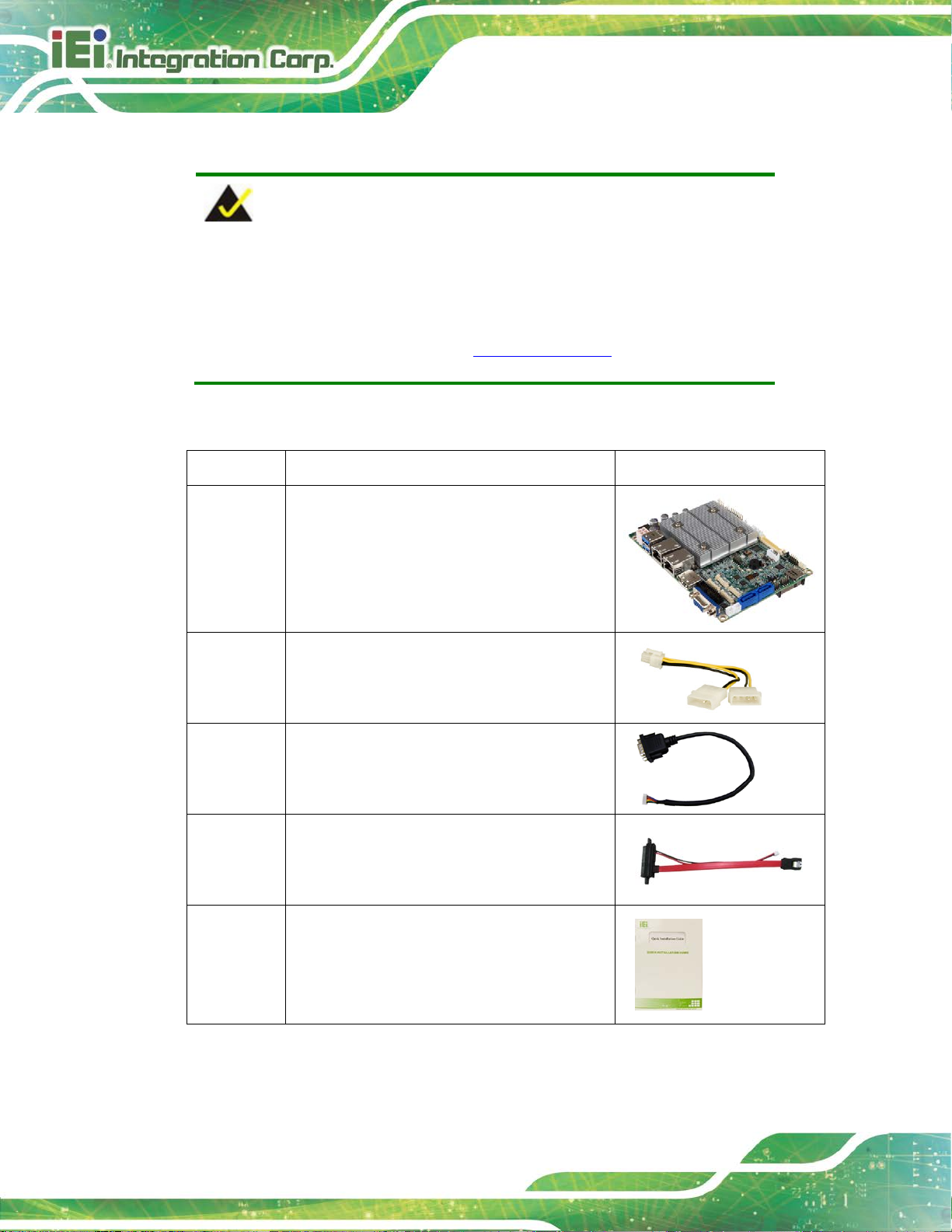
The WAFER-AL is shipped with the following components:
Quantity Item and Part Number Image
1 WAFER-AL single board computer
1 Power cable
1 RS-232/422/485 cable
.
2 SATA and power cable
1 Quick Installation Guide
Page 27
WAFER-AL SBC
Page 13
2.4 Optional Items
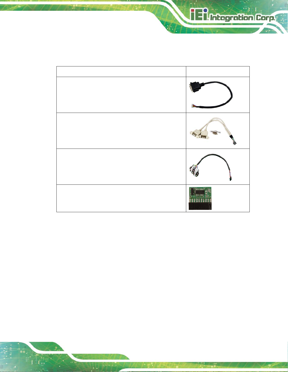
The following are optional components which may be separately purchased:
Item and Part Number Image
RS-232/422/485 cable, 250 mm, p=1.25
(P/N : 32005-003500-200-RS)
Dual USB port cable, 210mm, p=2.0 mm
(P/N: 32001-008600-200-RS)
Audio cable, 300mm, p=2.0 mm
(P/N: 32007-005200-200-RS)
Infineon TPM 2.0 module, 20-pin, firmware v5.5
(P/N: TPM-IN02-R20)
Page 28

WAFER-AL SBC
Page 14
Chapter
3
3 Connectors
Page 29
WAFER-AL SBC
Page 15
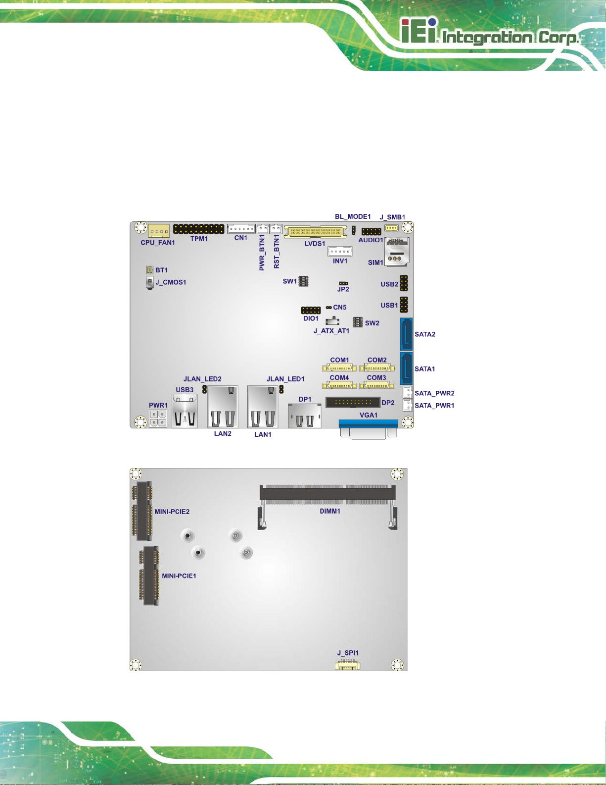
3.1 Peripheral Interface Connectors
This chapter details all the jumpers and connectors.
3.1.1 WAFER-AL Layout
The figures below show all the connectors and jumpers.
Figure 3-1: Connector and Jumper Locations (Front Side)
Figure 3-2: Connector and Jumper Locations (Solder Side)
Page 30

WAFER-AL SBC
Page 16
3.1.2 Peripheral Interface Connectors
The table below lists all the connectors on the board.
Connector Type Label
+12V DC-IN power connector 4-pin Molex PWR1
Audio connector 10-pin header AUDIO1
Battery connector 2-pin wafer BT1
Digital I/O connector 10-pin header DIO1
Fan connector, CPU 4-pin wafer CPU_FAN1
iDP connector (optional) 20-pin box header DP2
LVDS backlight inverter connector 5-pin wafer INV1
LVDS LCD connector 40-pin crimp LVDS1
LAN LED connectors 2-pin header JLAN_LED1,
JLAN_LED2
Memory slot 204-pin SO-DIMM DIMM1
mSATA module slot PCIe Mini slot MINI-PCIE1
PCIe Mini card slot PCIe Mini slot MINI-PCIE2
Power and HDD LED connector 6-pin wafer CN1
Power button connector 2-pin wafer PWR_BTN1
Reset button connector 2-pin wafer RST_BTN1
RS-232 serial port connectors 9-pin wafer COM3, COM4
RS-232/422/485 serial port connectors 9-pin wafer COM1, COM2
SATA 6Gb/s connectors 7-pin SATA connector SAT A1, SATA2
SATA power connectors 2-pin wafer SATA_PWR1,
SATA_PWR2
Page 31
WAFER-AL SBC
Page 17
SIM card slot Micro SIM card slot SIM1
SMBus/I2C connector 4-pin wafer J_SMB1
SPI Flash Connector 6-pin wafer J_SPI1
TPM connector 20-pin header TPM1
USB 2.0 connector 8-pin header USB1, USB2
EC firmware update connector
(for internal use only)
Table 3-1: Peripheral Interface Connectors
3.1.3 External Interface Panel Connectors
The table below lists the connectors on the external I /O panel.
Connector Type Label
DisplayPort++ connector DP++ DP1
LAN connectors RJ-45 LAN1, LAN2
USB 3.0 connectors USB 3.0 USB3
VGA connector DB-9 VGA1
2-pin header CN5
Table 3-2: Rear Panel Connectors
Page 32

WAFER-AL SBC
Page 18
3.2 Internal Peripheral Connectors
The section describes all of the connectors on the WAFER-AL.
3.2.1 +12V DC-IN Power Connector
CN Label: PWR1
CN Type:
CN Location:
CN Pinouts:
The connector supports the +12V power supply.
Figure 3-3: +12V DC-IN Power Connector Location
4-pin Molex, p=4.2 mm
See Figure 3-3
See Table 3-3
PIN NO. DESCRIPTION PIN NO. DESCRIPTION
1 GND 2 GND
3 +12V 4 +12V
Table 3-3: +12V DC-IN Power Connector Pinouts
Page 33

WAFER-AL SBC
Page 19
3.2.2 Audio Connector
CN Label:
CN Type:
CN Location:
CN Pinouts:
The audio connector is connected to external audio devices including speakers and
microphones for the input and output of audi o si gnals to and from the system.
AUDIO1
10-pin header, p=2.00 mm
See Figure 3-4
See Table 3-4
Figure 3-4: Audio Connector Location
PIN NO. DESCRIPTION PIN NO. DESCRIPTION
1 LINE-OUT_R 2 LINE-IN_R
3 AUD_GND 4 AUD_GND
5 LINE-OUT_L 6 LINE-IN_L
7 AUD_GND 8 AUD_GND
9 MIC_R 10 MIC_L
Table 3-4: Audio Connector Pinouts
Page 34

WAFER-AL SBC
Page 20
Risk of explosion if battery is replaced by an incorrect type. Only
spose of used batteries according to instructions and local
3.2.3 Battery Connector
CAUTION:
certified engineers should replace the on-board bat tery.
Di
regulations.
NOTE:
It is recommended to attach the RTC battery onto the system chassis
in which the WAFER-AL is installed.
CN Label:
CN Type:
CN Location:
CN Pinouts:
The battery connector is connected to the system battery. The battery provides power to
the system clock to retain the time when power is turned off.
BT1
2-pin wafer, p=1.25 mm
See Figure 3-5
See Table 3-5
Figure 3-5: Battery Connector Location
Page 35

WAFER-AL SBC
Page 21
Pin Description
1 VBAT+
2 GND
Table 3-5: Battery Connector Pinouts
3.2.4 Digital I/O Connector
CN Label: DIO1
CN Type:
CN Location:
CN Pinouts:
The 8-bit digital I/O connector provides programmable input and output for external
devices.
10-pin header, p=2.00 mm
See Figure 3-6
See Table 3-6
Figure 3-6: Digital I/O Connector Location
PIN NO. DESCRIPTION PIN NO. DESCRIPTION
1 GND 2 VCC
3 DOUT3 4 DOUT2
5 DOUT1 6 DOUT0
7 DIN3 8 DIN2
9 DIN1 10 DIN0
Table 3-6: Digital I/O Connector Pinouts
Page 36

WAFER-AL SBC
Page 22
3.2.5 Fan Connector
CN Label: CPU_FAN1
CN Type:
CN Location:
CN Pinouts:
The fan connector attaches to a cooling fan.
Figure 3-7: Fan Connector Location
4-pin wafer, p=2.54 mm
See Figure 3-7
See Table 3-7
Pin Description
1 GND
2 +V12S
3 Rotation Signal
4 PWM Control Signal
Table 3-7: Fan Connector Pinouts
Page 37

WAFER-AL SBC
Page 23
3.2.6 iDP Connector (Optional)
CN Label: DP2
CN Type:
CN Location:
CN Pinouts:
20-pin box header, p=2.00 m m
See Figure 3-8
See Table 3-8
The internal DisplayPort (iDP) connector supports HDMI, LVDS, VGA, DVI and
DisplayPort devices with up to 2560x1600 resolution. The iDP connector is only available
in iDP SKUs.
Figure 3-8: iDP Connector Location
Pin Description Pin Description
1 HPD 2 AUXP
3 GND 4 AUXN
5 NC 6 GND
7 GND 8 LANE2P
9 LANE3P 10 LANE2N
11 LANE3N 12 GND
13 GND 14 LANE0P
15 LANE1P 16 LANE0N
17 LANE1N 18 +3.3V
19 +5V 20 NC
Table 3-8: iDP Connector Pinouts
Page 38

WAFER-AL SBC
Page 24
3.2.7 LVDS Backlight Inverter Connector
CN Label: INV1
CN Type:
CN Location:
CN Pinouts:
5-pin wafer, p=2.00 mm
See Figure 3-9
See Table 3-9
The backlight inverter connector provide s power to an LCD panel.
Figure 3-9: Backlight Inverter Connector Location
Pin Description
1 LCD_BKLTCTL
2 GND
3 +12V
4 GND
5 BACKLIGHT ENABLE
Table 3-9: Backlight Inverter Connector Pinouts
Page 39
WAFER-AL SBC
Page 25
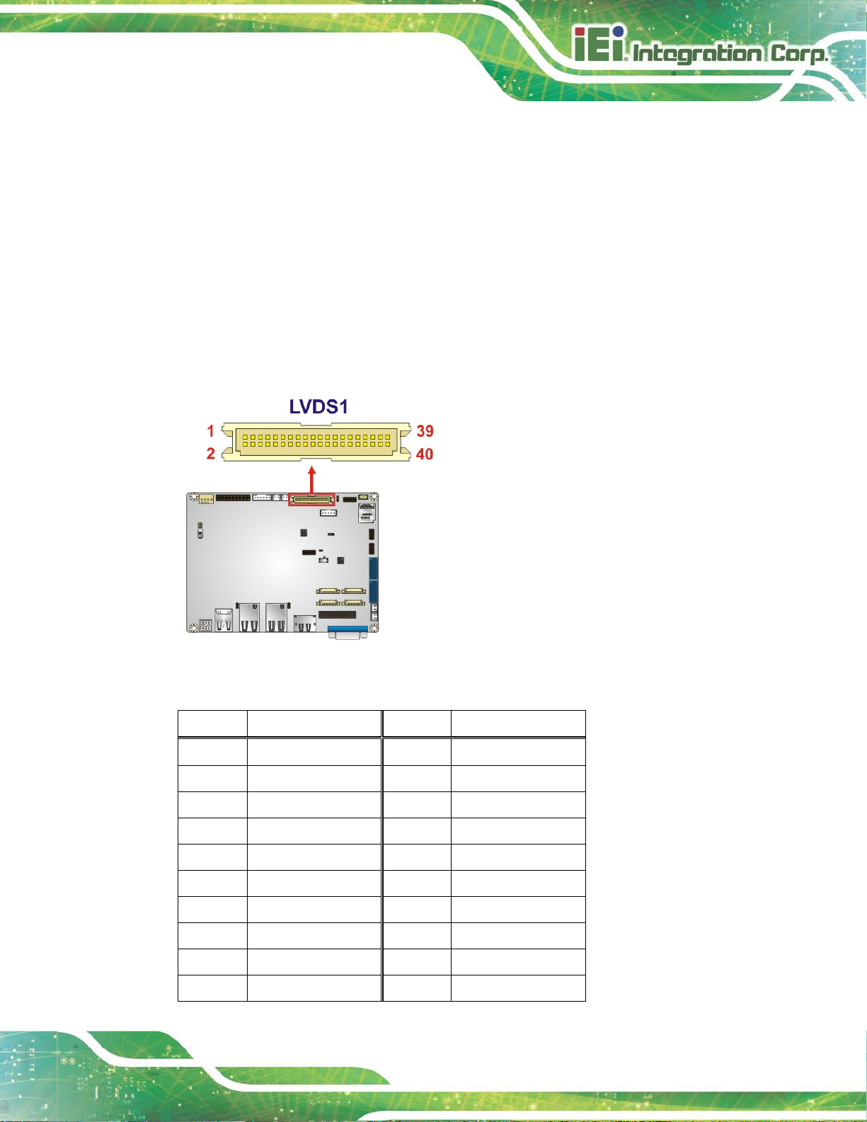
3.2.8 LVDS LCD Connect or
CN Label: LVDS1
CN Type:
CN Location:
CN Pinouts:
40-pin crimp, p=1.25 mm
See Figure 3-10
See Table 3-10
The LVDS connector is for an LCD panel connecte d to the board. The voltage provided to
the monitor connected to the LVDS connector is set to 3.3 V by default. To change the
setting, refer to Section 4.7.3.
Figure 3-10: LVDS Connector Location
Pin Description Pin Description
1 GROUND 2 GROUND
3 LVDS_A_TX0-N 4 LVDS_A_TX1-N
5 LVDS_A_TX0-P 6 LVDS_A_TX1-P
7 GROUND 8 GROUND
9 LVDS_A_TX2-N 10 LVDS_A_TXCLK-N
11 LVDS_A_TX2-P 12 LVDS_A_TXCLK-P
13 GROUND 14 GROUND
15 LVDS_A_TX3-N 16 LVDS_B_TX0-N
17 LVDS_A_TX3-P 18 LVDS_B_TX0-P
19 GROUND 20 GROUND
Page 40

WAFER-AL SBC
Page 26
Pin Description Pin Description
21 LVDS_B_TX1-N 22 LVDS_B_TX2-N
23 LVDS_B_TX1-P 24 LVDS_B_TX2-P
25 GROUND 26 GROUND
27 LVDS_B_TXCLK-N 28 LVDS_B_TX3-N
29 LVDS_B_TXCLK-P 30 LVDS_B_TX3-P
31 GROUND 32 GROUND
33 GROUND 34 GROUND
35 +LCD VCC 36 +LCD VCC
37 +LCD VCC 38 +LCD VCC
39 +LCD VCC 40 +LCD VCC
Table 3-10: LVDS Connector Pinouts
3.2.9 LAN LED Connectors
CN Label: JLAN_LED1, JLAN_LED2
CN Type:
CN Location:
CN Pinouts:
The LAN LED connectors connect to the LAN link LEDs on the system.
2-pin header, p=2.0 0 mm
See Figure 3-11
See Table 3-11
Figure 3-11: LAN LED Connector Locations
Page 41

WAFER-AL SBC
Page 27
Pin Description
1 +3.3V
2 LAN1_LED_LINK#_ACT
Table 3-11: LAN1 LED Connector (JLAN_LED1) Pinouts
Pin Description
1 +3.3V
2 LAN2_LED_LINK#_ACT
Table 3-12: LAN2 LED Connector (JLAN_LED2) Pinouts
3.2.10 mSATA Module Slot
CAUTION:
If an mSATA module is installed in the mSATA slot (MINI-PCIE1), the
SATA port 2 (SATA2) will be disabled. Choose either the SATA2
connector or the mSATA module for storage.
CN Label: MINI-PCIE1
CN Type:
CN Location:
CN Pinouts:
The PCIe Mini card slot supports mSATA modules or PCIe Mini cards with USB interface.
Half-size/Full-size PCIe Mini card slot
See Figure 3-12
See Table 3-13
Page 42

WAFER-AL SBC
Page 28
Figure 3-12: mSATA Module Slot Location
Pin Description Pin Description
1 PCIE_WAKE# 2 VCC3
3 N/C 4 GND
5 N/C 6 1.5V
7 N/C 8 N/C
9 GND 10 N/C
11 PCIE_CLK# 12 N/C
13 PCIE_CLK 14 N/C
15 GND 16 N/C
17 N/C 18 GND
19 N/C 20 N/C
21 GND 22 PCIRST#
23 PCIE_RXN (SATA_RX+) 24 N/C
25 PCIE_RXP (SATA_RX-) 26 GND
27 GND 28 1.5V
29 GND 30 SMBCLK
31 PCIE_TXN (SATA_TX-) 32 SMBDATA
33 PCIE_TXP (SATA_TX+) 34 GND
35 GND 36 USBD37 GND 38 USBD+
39 VCC3 40 GND
41 VCC3 42 N/C
43 GND 44 N/C
45 N/C 46 N/C
47 N/C 48 1.5V
49 N/C 50 GND
Page 43
WAFER-AL SBC
Page 29
Pin Description Pin Description
51 N/C 52 VCC3
Table 3-13: mSATA Module Slot Pinouts
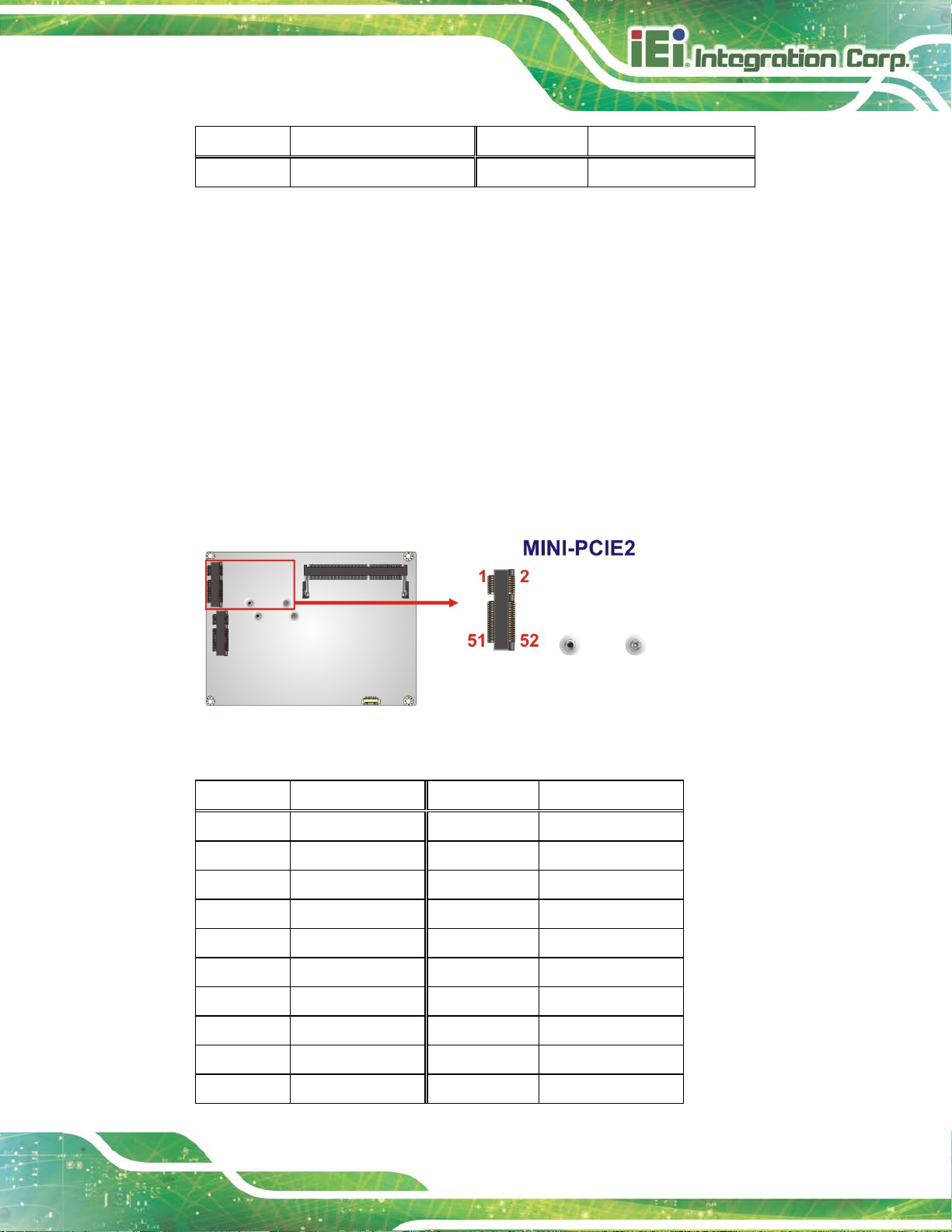
3.2.11 PCIe Mini Card Slot
CN Label: MINI-PCIE2
CN Type:
CN Location:
CN Pinouts:
Half-size/Full-size PCIe Mini card slot
See Figure 3-13
See Table 3-14
The PCIe Mini card slot is for installing a PCIe Mini expansion card with USB interface,
such as 3G modules.
Figure 3-13: PCIe Mini Card Slot Location
Pin Description Pin Description
1 PCIE_WAKE# 2 VCC3
3 N/C 4 GND
5 N/C 6 1.5V
7 N/C 8 UIM_PWR
9 GND 10 UIM_DATA
11 PCIE_CLK# 12 UIM_CLK
13 PCIE_CLK 14 UIM_RST
15 GND 16 UIM_VPP
17 N/C 18 GND
19 N/C 20 N/C
Page 44

WAFER-AL SBC
Page 30
Pin Description Pin Description
21 GND 22 PCIRST#
23 PCIE_RXN 24 N/C
25 PCIE_RXP 26 GND
27 GND 28 1.5V
29 GND 30 SMBCLK
31 PCIE_TXN 32 SMBDATA
33 PCIE_TXP 34 GND
35 GND 36 USBD37 GND 38 USBD+
39 VCC3 40 GND
41 VCC3 42 N/C
43 GND 44 N/C
45 N/C 46 N/C
47 N/C 48 1.5V
49 N/C 50 GND
51 N/C 52 VCC3
Table 3-14: PCIe Mini Card Slot Pinouts
Page 45

WAFER-AL SBC
Page 31
3.2.12 Power and HDD LED Connector
CN Label: CN1
CN Type:
CN Location:
CN Pinouts:
6-pin wafer , p=2.00 mm
See Figure 3-14
See Table 3-15
The CN1 connector connects to power and HDD LED indicators.
Figure 3-14: Power and HDD LED Connector Location
Pin Description
1 VCC
2 GND
3 PWR_LED+
4 PWR_LED5 HDD_LED+
6 HDD_LED-
+5V
Power LED
HDD LED
Table 3-15: Power and HDD LED Connector Pinouts
Page 46

WAFER-AL SBC
Page 32
3.2.13 Power Button Connector
CN Label:
CN Type:
CN Location:
CN Pinouts:
The power button connector connects to a power button.
PWR_BTN1
2-pin wafer, p=2.00 mm
See Figure 3-15
See Table 3-16
Figure 3-15: Power Button Connector Location
Pin Description
1 PWR_BTN+
2 PWR_BTN-
Table 3-16: Power Button Connector Pinouts
Page 47

WAFER-AL SBC
Page 33
3.2.14 Reset Button Connector
CN Label:
CN Type:
CN Location:
CN Pinouts:
The reset button connector connects to a reset button.
RST_BTN1
2-pin wafer, p=2.00 mm
See Figure 3-16
See Table 3-17
Figure 3-16: Reset Button Connector Location
Pin Description
1 RESET+
2 RESET-
Table 3-17: Reset Button Connector Pinouts
Page 48
WAFER-AL SBC
Page 34
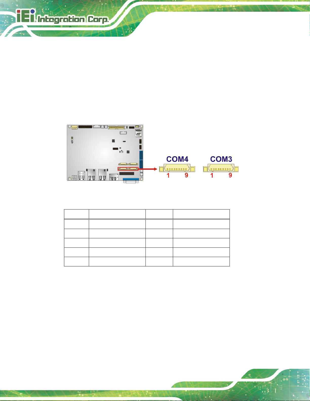
3.2.15 RS-232 Serial Port Connectors
CN Label: COM3, COM4
CN Type:
CN Location:
CN Pinouts:
9-pin wafer, p=1.25 mm
See Figure 3-17
See Table 3-18
The serial connectors provide RS-232 connection.
Figure 3-17: RS-232 Serial Port Connector Locations
PIN NO. DESCRIPTION PIN NO. DESCRIPTION
1 DCD 2 DSR
3 RXD 4 RTS
5 TXD 6 CTS
7 DTR 8 RI
9 GND
Table 3-18: RS-232 Serial Port Connector Pinouts
Page 49

WAFER-AL SBC
Page 35
3.2.16 RS-232/422/485 Serial Port Connectors
CN Label: COM1, COM2
CN Type:
CN Location:
CN Pinouts:
9-pin wafer, p=1. 25 m m
See Figure 3-18
See Table 3-19
These two connectors provide RS-232, RS-422 or RS-485 communications. The default
mode is set to RS-232 by the on-board switch. To configure the connectors as RS-422 or
RS-485, please refer to Section 4.7.6.
Figure 3-18: RS-232/422/485 Connector Locations
Pin RS-232 RS-422 RS-485
1 DCD TXD- DATA2 DSR -- -3 RXD TXD+ DATA+
4 RTS -- -5 TXD RXD+ -6 CTS -- -7 DTR RXD- -8 RI -- -9 GND -- --
Table 3-19: RS-232/422/485 Connector Pinouts
Use the RS-232/422/485 cable to connect to a serial device. The pinouts of the DB-9
connector are listed below.
Page 50

WAFER-AL SBC
Page 36
PIN NO. RS-232 RS-422 RS-485
1 DCD TXD422- TXD4852 RXD TXD422+ TXD485+
3 TXD RXD422+ -4 DTR RXD422- -5 GND -- -6 DSR -- -7 RTS -- -8 CTS -- -9 RI -- --
Table 3-20: RS-232/422/485 Cable Pinouts
3.2.17 SATA 6Gb/s Connectors
CN Label:
CN Type:
CN Location:
The SATA 6Gb/s connector is connected to a SATA 6Gb/s device. The SATA 6Gb/s
device transfers data at speeds as high as 6Gb/s.
SATA1, SATA2
7-pin SATA connector
See Figure 3-19
Figure 3-19: SATA 6Gb/s Connector Locations
Page 51

WAFER-AL SBC
Page 37
2) will be disabled. Choose either the SATA2
CAUTION:
If an mSATA module is installed in the mSATA slot (MINI-PCIE1), the
SATA port 2 (SATA
connector or the mSATA module for storage.
3.2.18 SATA Power Connectors
CN Label:
CN Type:
CN Location:
CN Pinouts:
The SATA power connector provides +5 V power output to the SATA connector.
Figure 3-20: SATA Power Connector Locations
SATA_PWR1, SATA_PWR2
2-pin wafer, p=2.00 mm
See Figure 3-20
See Table 3-21
Pin Description
1 +5V
2 GND
Table 3-21: SATA Power Connector Pinouts
Page 52

WAFER-AL SBC
Page 38
3.2.19 SIM Card Slot
CN Label: SIM1
CN Type:
CN Location:
The SIM card slot accepts a micro SIM card for network communic ati on.
Figure 3-21: SIM Card Slot Location
Micro SIM card slot
See Figure 3-21
3.2.20 SMBus/I2C Connector
CN Label: J_SMB1
CN Type:
CN Location:
CN Pinouts:
The SMBus/I
Figure 3-22: SMBus/I
4-pin wafer, p=1. 25 m m
See Figure 3-22
See Table 3-22
2
C connector provides low-speed system manageme nt communications.
2
C Connector Location
Page 53

WAFER-AL SBC
Page 39
Pin Description
1 GND
2 SMBus (I2C) DATA
3 SMBus (I2C) CLK
4 +5V
3.2.21 SPI Flash Connector
CN Label: J_SPI1
Table 3-22: SMBus/I2C Connector Pinouts
CN Type:
CN Location:
CN Pinouts:
The 6-pin SPI Flash connector is used to flash the B IOS.
6-pin wafer , p=1.25 mm
See Figure 3-23
See Table 3-23
Figure 3-23: SPI Flash Connector Location
Pin Description
1 VCC
2 SPI_CS
3 SPI_SO
4 SPI_CLK
5 SPI_SI
6 GND
Table 3-23: SPI Flash Connector Pinouts
Page 54

WAFER-AL SBC
Page 40
3.2.22 TPM Connector
CN Label:
CN Type:
CN Location:
CN Pinouts:
TPM1
20-pin header, p=2.54 mm
See Figure 3-24
See Table 3-24
The Trusted Platform Module (TPM) connector secures the system on bootup.
Figure 3-24: TPM Connector Location
Pin Description Pin Description
1 LCLK 2 GND
3 LFRAME# 4 KEY
5 LRERST# 6 +5V
7 LAD3 8 LAD2
9 +3.3V 10 LAD1
11 LAD0 12 GND
13 SCL 14 SDA
15 SB3V 16 SERIRQ
17 GND 18 GLKRUN#
19 LPCPD# 20 LDRQ#
Table 3-24: TPM Connector Pinouts
Page 55

WAFER-AL SBC
Page 41
3.2.23 USB 2.0 Connectors
CN Label:
CN Type:
CN Location:
CN Pinouts:
These USB connectors provide four USB 2.0 ports by dual-port USB cable.
USB1, USB2
8-pin header, p=2.00 mm
See Figure 3-25
See Table 3-25
Figure 3-25: USB Connector Locations
PIN NO. DESCRIPTION PIN NO. DESCRIPTION
1 USB_VCC 2 GND
3 DATA- 4 DATA+
5 DATA+ 6 DATA7 GND 8 USB_VCC
Table 3-25: USB Connector Pinouts
Page 56

WAFER-AL SBC
Page 42
3.3 External Peripheral Interface Connector Panel
Figure 3-26 shows the WAFER-AL external peripheral interface connector (EPIC) panel.
The EPIC panel consists of the following:
1 x DisplayPort++ connector
2 x GbE LAN connector
2 x USB 3.0 connector
1 x VGA connector
Figure 3-26: External Peripheral Interface Co nn ector
3.3.1 DisplayPort++ Connector
CN Label: DP1
CN Type:
CN Location:
CN Pinouts:
The DisplayPort++ connector (Dual-mode DisplayPort) can connect to an HDMI or
DisplayPort device. The DisplayPort++ connectors support up to 4096x2160 resolutions at
60 Hz.
DisplayPort
See Figure 3-26
See Table 3-26
Page 57

WAFER-AL SBC
Page 43
Pin HDMI DisplayPort
1 TMDS DATA2+ L0P
2 GND GND
3 TMDS DATA2- L0N
4 TMDS DATA1+ L1P
5 GND GND
6 TMDS DATA1- L1N
7 TMDS DATA0+ L2P
8 GND GND
9 TMDS DATA0- L2N
10 TMDS CLK+ L3P
11 GND GND
12 TMDS CLK- L3N
13 DP_HDMI_SEL DP_HDMI_SEL
14 NC NC
15 SCL AUXP
16 GND GND
17 SDA AUXN
18 HDMI HPD DP HPD
19 GND GND
20 HDMI PWR DP PWR
Table 3-26: HDMI Connector Pinouts
Figure 3-27: HDMI Connector Pinout Locations
Page 58
WAFER-AL SBC
Page 44
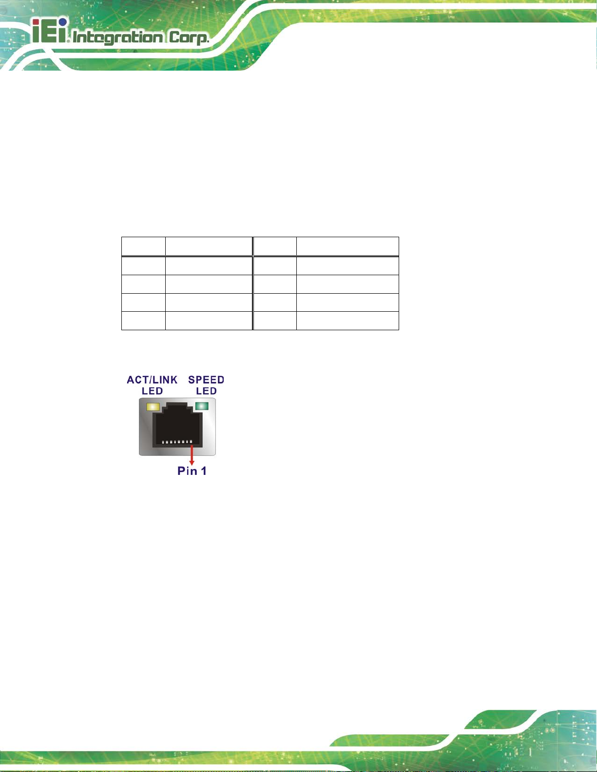
3.3.2 LAN Connectors
CN Label: LAN1, LAN2
CN Type:
CN Location:
CN Pinouts:
The LAN connector connects to a local network.
RJ-45
See Figure 3-26
See Figure 3-28 and Table 3-27
Pin Description Pin Description
1 LAN_MDI0+ 7 LAN_MDI2+
2 LAN_MDI0- 8 LAN_MDI23 LAN_MDI1+ 9 LAN_MDI3+
4 LAN_MDI1- 10 LAN_MDI3-
Table 3-27: LAN Pinouts
Figure 3-28: LAN Connector
3.3.3 USB Connectors
CN Label: USB1
CN Type:
CN Location:
CN Pinouts:
The WAFER-AL has two external USB 3.0 ports. The USB connector can be connect ed to
a USB 2.0 or USB 3.0 device. The pinouts of USB 3.0 connectors are shown below.
USB 3.0 ports
See Figure 3-26
Table 3-28
See
Page 59
WAFER-AL SBC
Page 45
Pin Description Pin Description
1 USB_VCC 10 USB_VCC
2 USB2_D0- 11 USB2_D03 USB2_D0+ 12 USB2P0_D0+
4 GND 13 GND
5 USB3P0_RXDN1 14 USB3P0_RXDN2
6 USB3P0_RXDP1 15 USB3P0_RXDP2
7 GND 16 GND
8 USB3P0_TXDN1 17 USB3P0_TXDN2
9 USB3P0_TXDP1 18 USB3P0_TXDP2
Table 3-28: USB 3.0 Port Pinouts
Figure 3-29: USB 3.0 Port Pinout Locations
3.3.4 VGA Connector
CN Label: VGA1
CN Type:
CN Location:
CN Pinouts:
15-pin Female
See Figure 3-26
See Figure 3-30 and Table 3-29
The external VGA port connects to a monitor t hat accepts a standard VGA input.
Page 60

WAFER-AL SBC
Page 46
Figure 3-30: VGA Connector
Pin Description Pin Description
1 RED 2 GREEN
3 BLUE 4 NC
5 GND 6 GND
7 GND 8 GND
9 VCC / NC 10 GND
11 NC 12 DDC DAT
13 HSYNC 14 VSYNC
15 DDCCLK
Table 3-29: VGA Connector Pinouts
Page 61

WAFER-AL SBC
Page 47
Chapter
4
4 Installation
Page 62
WAFER-AL SBC
Page 48
Failure to take ESD precautions during the installation of the
4.1 Anti-static Precautions
WARNING:
WAFER-AL may result in permanent damage to the WAFER-AL and
severe injury to the user.
Electrostatic discharge (ESD) can cause serious damage to electronic components,
including the WAFER-AL. Dry climates are especially susceptible to ESD. It is therefore
critical that whenever the WAFER-AL or any other electrical component is handled, the
following anti-static precautions are strictly adhered to.
Wear an anti-static wristband: Wearing a simple anti-static wristband can
help to prevent ESD from damaging the board.
Self-grounding Before handling the board, touch any grounded conducting
material. During the time the board is handled, f requently touch any
conducting materials that are connected to the ground.
Use an anti-static pad: When configuring the WAFER-AL, place it on an
anti-static pad. This reduces the possibility of ESD damaging the WAFER-AL.
Only handle the edges of the PCB: When handling the PCB, hold the PCB
by the edges.
4.2 Installation Considerations
NOTE:
The following installation notices and installation considerations should
be read and understood before installation. All instal l ation notices must
be strictly adhered to. Failing to adhere to these precautions may lead
to severe damage and injury to the person performing the installation.
Page 63
WAFER-AL SBC
Page 49
The installation instructions described in this manual should be carefully
WARNING:
followed in order to prevent damage to the WAFER-AL, WAFER-AL
components and injury to the user.
Before and during the installation please DO the following:
Read the user manual:
o The user manual provides a complete description of the WAFER-AL
installation instructions and configuration opt i ons.
Wear an electrostatic discharge cuff (ESD):
o Electronic components are easily damaged by ESD. Wearing an ESD cuff
removes ESD from the body and helps prevent ESD damage.
Place the WAFER-AL on an antistatic pad:
o When installing or configuring the motherboa rd, place it on an antistatic
pad. This helps to prevent potential ESD damage.
Turn all power to t he WAFER-AL off:
o When working with the WAFER-AL, make sure that it is disconnected
from all power supplies and that no elect ricity is b eing f ed into the sy stem.
Before and during the installation of the WAFER-AL DO NOT:
Remove any of the stickers on the PCB board. These st ickers a re required f or
warranty validation.
Use the product before verifying all the cables and power connectors are
properly connected.
Allow screws to come in contact with the P CB circuit, connector pins, or its
components.
Page 64

WAFER-AL SBC
Page 50
2) will be disabled. Choose either the SATA2
4.3 SO-DIMM Installation
To install an SO-DIMM, please follow the step s below and refer to Figure 4-1.
Figure 4-1: SO-DIMM Installation
Step 1: Locate the SO-DIMM socket. Place the board on an anti-static mat.
Step 2: Align the SO-DIMM with the socket. Align the notch on the memory with the
notch on the memory socket.
Step 3: Insert the SO-DIMM. Push the memory in at a 20º angle. (See Figure 4-1)
Step 4: Seat the SO-DIMM. Gently push downwards and the arms clip into place. (See
Figure 4-1)
4.4 mSATA Module Installation
CAUTION:
If an mSATA module is installed in the mSATA slot (MINI-PCIE1), the
SATA port 2 (SATA
connector or the mSATA module for storage.
The full-size/half-size PCIe Mini card slot (MINI-PCIE1) allows installation of an mSATA
module. To install an mSATA module, please follow the steps below.
Page 65

WAFER-AL SBC
Page 51
4.4.1 Full-size mSATA Module Installation
To install a full-size mSATA module, please follow the steps below.
Step 1: Locate the PCIe Mini slot (MINI-PCIE1). See Chapter 3.
Step 2: Remove the retention screw as shown in Figure 4-2.
Figure 4-2: Removing the Retention Screw
Step 3: Line up the notch on the mSATA module with the notch on the slot. Slide the
mSATA module into t he so ck et at an angle of about 20º (Figure 4-3).
Figure 4-3: Inserting the Full-size mSATA Module into the Slot at an Angle
Page 66

WAFER-AL SBC
Page 52
Step 4: Secure the mSATA module with the retenti on screw previously removed
(Figure 4-4). Step 0:
Figure 4-4: Securing the mSATA Module
4.4.2 Half-size mSATA Module Installation
To install a half-size mSATA module, please follow the steps below.
Step 1: Locate the PCIe Mini card slot (MINI-PCIE1). See Chapter 3.
Step 2: Remove the retention screw. Unscrew and remove the standoff secured on the
motherboard. See Figure 4-5.
Page 67

WAFER-AL SBC
Page 53
Figure 4-5: Removing the Retention Screw and the Standoff
Step 3: Install the previously removed standoff to the screw hole for the half-size mSATA
module (Figure 4-6).
Figure 4-6: Installing the Standoff
Step 4: Line up the notch on the card with the notch on the slot. Slide the mSATA
module into the slot at an angle of about 20º (Figure 4-7).
Page 68

WAFER-AL SBC
Page 54
Figure 4-7: Inserting the Half-size mSATA Module into the Slot at an Angle
Step 5: Secure the half-size mSATA module with the retention screw previously
removed (Figure 4-8). Step 0:
Figure 4-8: Securing the Half-size mSATA Module
Page 69

WAFER-AL SBC
Page 55
4.5 PCIe Mini Card Installation
The PCIe Mini card slot (MINI-PCIE2) allows installation of either a full-size or half-size
PCIe Mini card. To install a full-size PCIe Mini card, please refer to the steps described in
Section 4.4 above.
4.6 SIM Card Installation
To install a SIM card, please follow the steps below.
Step 1: Locate the SIM card slot. See Section 3.2.19.
Step 2: Unlock the SIM card slot cover by sliding the cover in the direction as shown by
the arrow in Figure 4-9.
Figure 4-9: Unlock SIM Card Slot Cover
Page 70

WAFER-AL SBC
Page 56
Step 3: Open the slot cover and place a SIM card onto the slot. The cut mark on the
corner should be facing away from the slot as shown in Figure 4-10.
Figure 4-10: SIM Card Installation
Step 4: Close the slot cover and lock it by sliding it in the direction as shown by the
arrow in Figure 4-11.
Figure 4-11: Lock SIM Card Slot Cover
Page 71

WAFER-AL SBC
Page 57
4.7 System Configuration
The system configuration is controlled by buttons, jumpers and switches. The system
configuration should be performed before inst al l ation.
4.7.1 AT/ATX Mode Select Switch
CN Label:
CN Type:
CN Location:
CN Settings:
The AT/ATX mode select switch specifies the systems power mode as AT or ATX.
AT/ATX mode select switch settings are shown in Table 4-1.
Setting Description
Short 1-2 ATX Mode (Default)
Short 2-3 AT Mode
Table 4-1: AT/ATX Mode Select Switch Settings
The location of the AT/ATX mode select switch is sh own in Figure 4-12 below.
J_ATX_AT1
Switch
See Figure 4-12
See Table 4-1
Figure 4-12: AT/ATX Mode Select Switch Location
Page 72

WAFER-AL SBC
Page 58
4.7.2 Clear CMOS Button
CN Label: J_CMOS1
CN Type:
CN Location:
If the WAFER-AL fails to boot due to improper BIOS settings, use the button to clear the
CMOS data and reset the system BIOS information. To c lear the CMOS, disconnect the
battery (BT1) and press the clear CMOS button for about 3 seconds.
The location of the clear CMOS button is shown in Figure 4-13
Button
See Figure 4-13
Figure 4-13: Clear CMOS Button Location
Page 73

WAFER-AL SBC
Page 59
may occur if the
wrong voltage is selected with this jumper. Please refer to the user
4.7.3 LVDS Voltage Select Jumper
WARNING:
Permanent damage to the screen and WAFER-AL
guide that came with the monitor to select t he correct voltage.
Jumper Label: JP2
Jumper Type:
Jumper Settings:
Jumper Location:
The LVDS voltage selection jumper allows setting the voltage provided to the monitor
connected to the LVDS connector.
Setting Description
Short 1-2 +3.3 V (Default)
Short 2-3 +5 V
Table 4-2: LVDS Voltage Select Jumper Settings
3-pin header, p=2.0 0 mm
See Table 4-2
See Figure 4-14
Figure 4-14: LVDS Voltage Select Jumper Location
Page 74

WAFER-AL SBC
Page 60
4.7.4 LVDS Backlight Mode Select Jumper
Jumper Label: BL_MODE1
Jumper Type:
Jumper Settings:
Jumper Location:
The LVDS backlight mode selection jumper allows setting the mode of the LVDS
backlight.
Setting Description
Short 1-2 PWM mode (Default)
Short 2-3 DC mode
Table 4-3: LVDS Backlight Mode Select Jumper Settings
3-pin header, p=2.00 mm
See Table 4-3
See Figure 4-15
Figure 4-15: LVDS Backlight Mode Select Jumper Location
Page 75
WAFER-AL SBC
Page 61
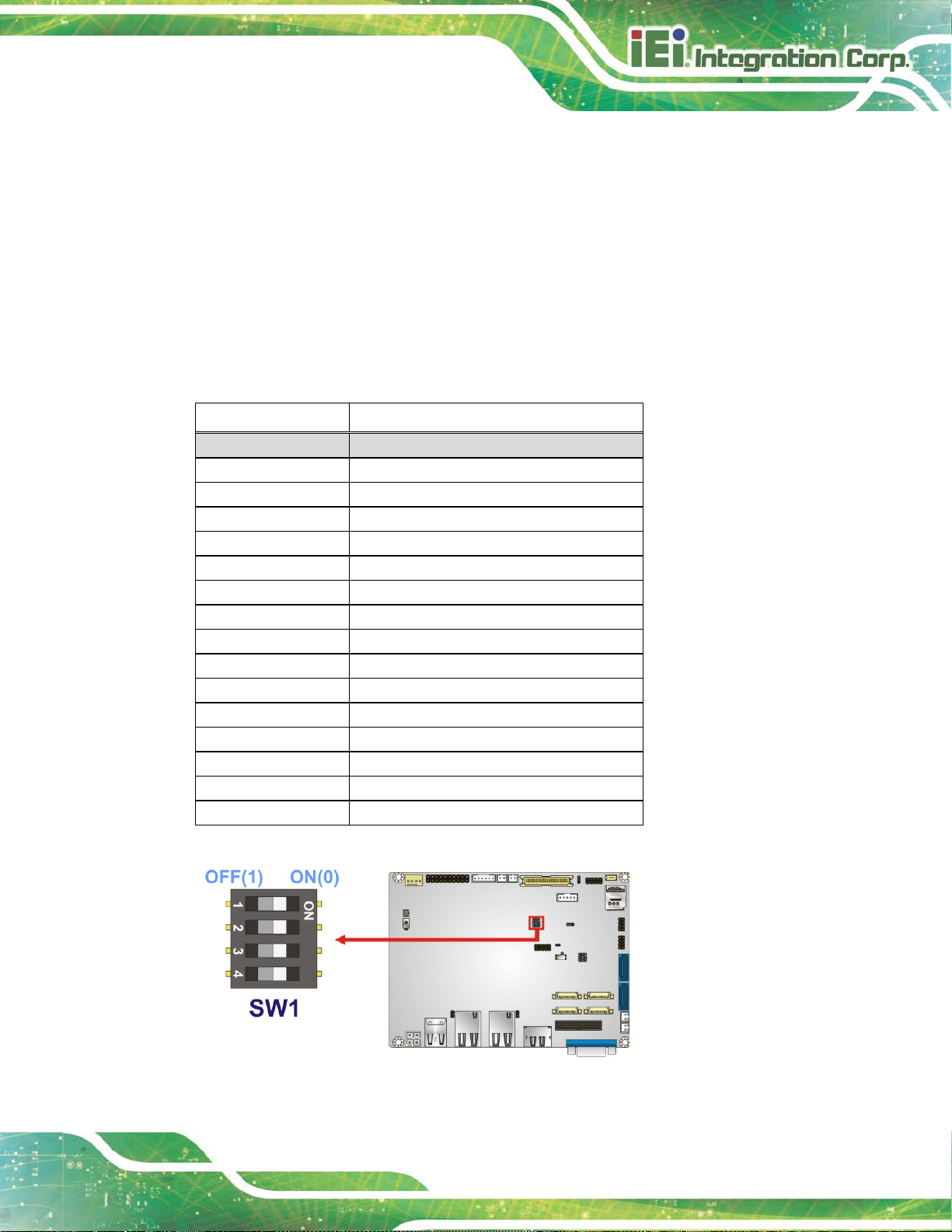
4.7.5 LVDS Pa nel Resolution Select Switch
Jumper Label: SW1
Jumper Type:
Jumper Settings:
Jumper Location:
DIP switch
See Table 4-4
See Figure 4-16
The SW1 selects the resolution of the LCD panel connected to the LVDS connector.
* ON=0, OFF=1; Single=S, Dual=D
SW1 (4-3-2-1) Description
0000 800x600 18-bit S (default)
0001 1024x768 18-bit S
0010 1024x768 24-bit S
0011 1280x768 18-bit S
0100 1280x800 18-bit S
0101 1280x960 18-bit S
0110 1280x1024 24-bit D
0111 1366x768 18-bit S
1000 1366x768 24-bit S
1001 1440x900 24-bit D
1010 1400x1050 24-bit D
1011 1600x900 24-bit D
1100 1680x1050 24-bit D
1101 1600x1200 24-bit D
1110 1920x1080 24-bit D
1111 1920x1200 24-bit D
Table 4-4: LVDS Panel Resolution Selection
Figure 4-16: LVDS Panel Resolution Select Switch Location
Page 76

WAFER-AL SBC
Page 62
4.7.6 RS-232/422/485 Mode Select Switch
Jumper Label: SW2
Jumper Type:
Jumper Settings:
Jumper Location:
DIP switch
See Table 4-5
See Figure 4-17
The SW2 selects RS-232/422/485 mode of the COM1 and COM2 serial ports.
SW2 (1) SW2 (2) Description
ON ON COM1 RS-422
ON OFF CO M1 RS-232 (Default)
OFF ON CO M1 RS-485
SW2 (3) SW2 (4) Description
ON ON COM2 RS-422
ON OFF CO M2 RS-232 (Default)
OFF ON COM2 RS-485
Table 4-5: RS-232/422/485 Mode Selection
Figure 4-17: RS-232/422/485 Mode Select Switch Location
Page 77

WAFER-AL SBC
Page 63
Airflow is critical for keeping components within recommended
operating temperatures. The chassis should have fans and vents as
4.8 Chassis Installation
4.8.1 Airflow
WARNING:
necessary to keep things cool.
The WAFER-AL must be installed in a chassis with ventilation holes on the sides allowing
airflow to travel through the heat sink surf ace. In a system with an individual power supply
unit, the cooling fan of a power supply can also help generate airflow through the board
surface.
4.8.2 Motherboard Installation
To install the WAFER-AL motherboard into the chassis please refer to the reference
material that came with the chassis.
4.9 Internal Peripheral Device Connections
This section outlines the installation of peripheral devices to the onboard connectors.
4.9.1 Audio Kit Installation
The Audio Kit that came with the WAFER-AL connects to the audio connector on the
WAFER-AL. The audio kit consists of three audio jacks. Mic-in connects to a microphone.
Line-in provides a stereo line-level input to connect to the output of an audio device.
Line-out, a stereo line-level output, connects to two amplified speakers. To install the
audio kit, please refer to the steps below:
Step 1: Locate the audio connector. The location of the 10-pin audio connector is
shown in Chapter 3.
Page 78
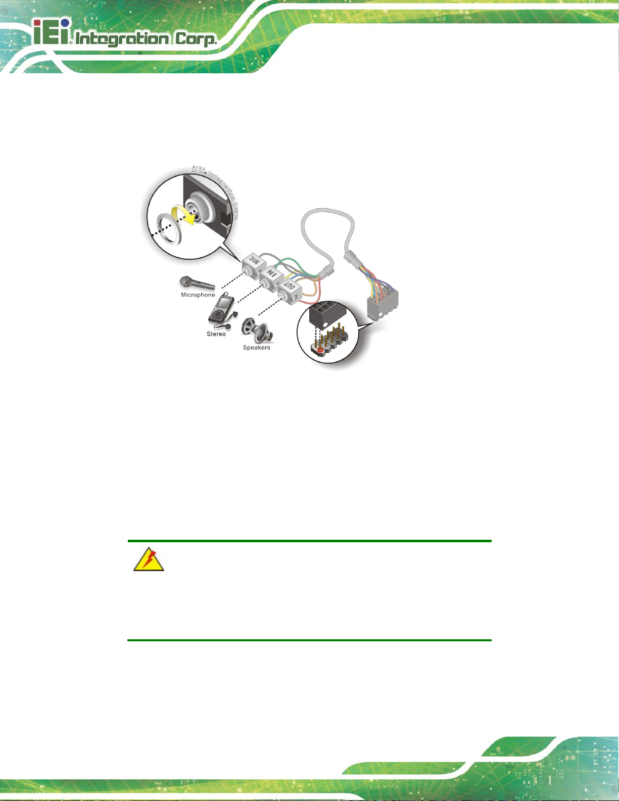
WAFER-AL SBC
Page 64
Step 2: Align pin 1. Align pin 1 on the on-board connector with pin 1 on the audio kit
connector. Pin 1 on the audio kit connector is indi cat ed with a white dot. See
Figure 4-18.
Figure 4-18: Audio Kit Cable Connection
Step 3: Connect the audio devices. Connect speakers to the line-out audio jack.
Connect the output of an audio device to the line-in a udi o j ack. Connect a
microphone to the mic-in audio jack.Step 0:
4.9.2 AT Power Connection
Follow the instructions below to connect the WAFER-AL to an AT powe r supply.
WARNING:
Disconnect the power supply power cord from its AC power source to
prevent a sudden power surge to the WAFER-AL.
Step 1: Locate the power cable. The power cable is shown in the packing list in
Chapter 2.
Page 79
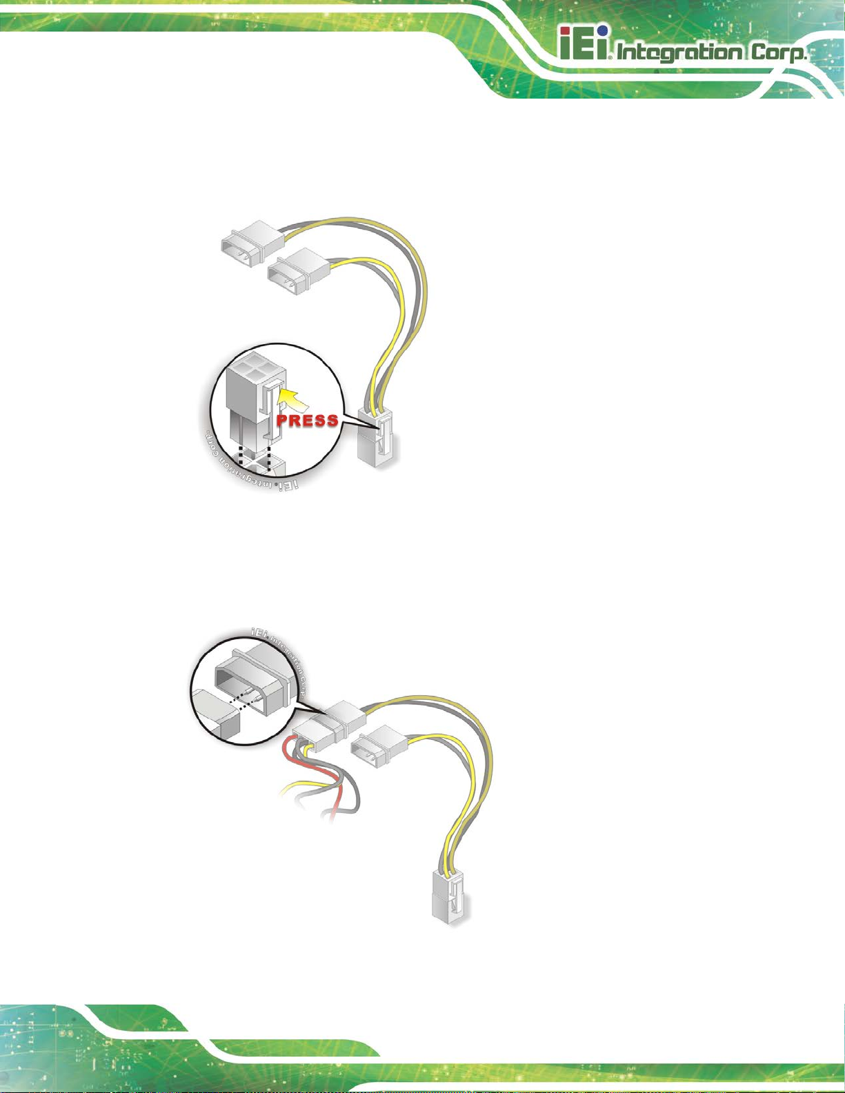
WAFER-AL SBC
Page 65
Step 2: Connect the Power Cable to the Motherboard. Connect the 4-pin (2x2) Molex
type power cable connector to the AT power connector on the motherboa rd. See
Figure 4-19.
Figure 4-19: Power Cable to Motherboard Connection
Step 3: Connect Power Cable to Power Supply. Connect one of the 4-pin (1x4) Molex
type power cable connectors to an AT power suppl y. See Figure 4-20. Step 0:
Figure 4-20: Connect Power Cable to Power Supply
Page 80

WAFER-AL SBC
Page 66
4.9.3 SATA Drive Connection
The WAFER-AL is shipped with two SATA cables. To connect the SATA drive to the
connector, please follow the steps below.
Step 1: Locate the SATA connector and the SATA po wer connector. The locations of
the connectors are shown in Chapter 3.
Step 2: Insert the cable connector. Insert the cable connector into the on-board SATA
drive connector and the SATA power connector. See Figure 4-21.
NOTE:
The connector locations in the following diagram are just for reference.
For the exact locations, please see Section 3.2.17 and Section 3.2.18.
Page 81

WAFER-AL SBC
Page 67
Figure 4-21: SATA Drive Cable Connection
Step 3: Connect the cable to the SATA disk. Connect the connector on the other end
of the cable to the connector at the back of the S AT A drive. See Figure 4-21.
Step 4: To remove the SATA cable from the SATA connector, press the clip on the
connector at the end of the cable. Step 0:
Page 82

WAFER-AL SBC
Page 68
Chapter
5
5 BIOS
Page 83

WAFER-AL SBC
Page 69
5.1 Introduction
The BIOS is programmed onto the BIOS chip. The BI OS setup pro gram allows changes to
certain system settings. This chapter outli nes t he options that can be changed.
NOTE:
Some of the BIOS options may vary throughout the life cycle of the
product and are subject to change without prior notice .
5.1.1 Starting Setup
The UEFI BIOS is activated when the computer is turned on. The setup program can be
activated in one of two ways.
1. Press the D
2. Press the D
appears on the screen. 0.
If the message disappears before the D
and try again.
ELETE or F2 key as soon as the system is turned on or
ELETE or F2 key when the “Press Del to enter SETUP” message
ELETE or F2 key is pressed, restart the computer
5.1.2 Using Setup
Use the arrow keys to highlight items, press ENTER to select, use the PageUp and
PageDown keys to change entries, press F1 for help and press E
keys are shown in Table 5-1.
Key Function
Up arrow Move to previous item
Down arrow Move to next item
Left arrow Move to the item on the left hand side
SC to quit. Navigation
Right arrow Move to the item on the right hand side
+ Increase the numeric value or make change s
Page 84

WAFER-AL SBC
Page 70
Key Function
- Decrease the numeric value or make changes
F1 key General help, only for Status Page Setup Menu and Option
Page Setup Menu
F2 key Load previous values.
F3 key Load optimized defaults
F4 key Save changes and Exit BIOS
Esc key Main Menu – Quit and not save changes into CMOS
St atus Page Setup Menu and Option Page Setup Menu --
Exit current page and return to M ai n M enu
Table 5-1: BIOS Navigation Keys
5.1.3 Getting Help
When F1 is pressed a small help window describing the appropriate keys to use and the
possible selections for the highlighted item appears. To ex it the Help Window press E
the F1 key again.
5.1.4 Unable to Reboot after Configuration Changes
If the computer cannot boot after changes to the system configuration is made, CMOS
defaults. Use the jumper described in Section 4.7.2.
5.1.5 BIOS Menu Bar
The menu bar on top of the BIOS screen has the foll owing main items:
Main – Changes the basic system configuration.
Advanced – Changes the advanced system settings.
Chipset – Changes the chip set settings.
Security – Sets User and Supervisor Passwords.
SC or
Boot – Changes the system boot configuration.
Save & Exit – Selects exit options and loads default set tings
Page 85

WAFER-AL SBC
Page 71
Aptio Setup Utility – Copyright (C) 2017 American Megatrends, Inc.
Main
Advanced
Chipset
Security
Boot
Save & Exit
Version 2.18.1263. Copyright (C) 2017 American Megatrends, Inc.
The following sections completely describe the configuration options found in the menu
items at the top of the BIOS screen and listed above.
5.2 Main
The Main BIOS menu (BIOS Menu 1) appears when the BIOS Setup program is entered.
The Main menu gives an overview of the basic syste m i nformation.
BIOS Information
BIOS Vendor American Megatrends
Core Version 5.12
Compliency UEFI 2.5; PI 1.4
Project Version B409AR09.BIN
Build Date and Time 01/09/2017 15:49:35
Platform firmware Information
BXT SOC B1
MRC Version 0.56
PUNIT FW 24
PMC FW 03.26
TXE FW 3.0.11.1131
ISH FW 4.1.0.3364
GOP 0.0.0036
CPU Flavor BXT Notebook/Desktop
Board ID Oxbow Hill CRB (06)
Fab ID FAB A
Memory Information
Total Memory 2048 MB
Memory Speed 1600 MHz
System Date [Fri 01/01/2010]
System Time [00:18:35]
Set the Date. Use Tab to
switch between Data
elements.
---------------------
: Select Screen
↑ ↓: Select Item
Enter Select
+/-: Change Opt.
F1: General Help
F2: Previous Values
F3: Optimized Defaults
F4: Save & Exit
ESC: Exit
BIOS Menu 1: Main
System Date [xx/xx/xx]
Use the System Date option to set the system date. Manually enter the day, month and
year.
Page 86

WAFER-AL SBC
Page 72
Aptio Setup Utility – Copyright (C) 2017 American Megatrends, Inc.
Main
Advanced
Chipset
Security
Boot
Save & Exit
Version 2.18.1263. Copyright (C) 2017 American Megatrends, Inc.
System Time [xx:xx:xx]
Use the System Time option to set the system time. Manually enter the hours, minutes
and seconds.
5.3 Advanced
Use the Advanced menu (BIOS Menu 2) to configure the CPU and peripheral devices
through the following sub-menus:
WARNING!
Setting the wrong values in the sections below may cause the system
to malfunction. Make sure that the settings made are compatible with
the hardware.
> Trusted Computing
> ACPI Settings
> F81866 Super IO Configuration
> F81866 H/W Monitor
> USB Configuration
> CPU Configuration
> RTC Wake Settings
> Power Saving Configuration
> Serial Port Console Redirection
> iEi Feature
BIOS Menu 2: Advanced
System ACPI Parameters.
----------------------
: Select Screen
↑ ↓: Select Item
Enter Select
F1 General Help
F2 Previous Values
F3 Optimized Defaults
F4 Save
ESC Exit
Page 87

WAFER-AL SBC
Page 73
Aptio Setup Utility – Copyright (C) 2017 American Megatrends, Inc.
Advanced
ESC Exit
Version 2.18.1263. Copyright (C) 2017 American Megatrends, Inc.
5.3.1 Trusted Computing
Use the Trusted Computing menu (BIOS Menu 3) to configure settings related to the
Trusted Computing Group (TCG) Truste d P l atform Module (TPM).
Configuration
Security Device Support [Disable]
NO Security Device Found
BIOS Menu 3: Trusted Computing
Security Device Support [Disable]
Use the Security Device Support option to configu re support for the security device.
Enables or Disables BIOS
support for security
device. O.S. will not
show Security Device.
TCG EFI protocol and
INT1A interface will not
be available.
----------------------
: Select Screen
↑ ↓: Select Item
Enter Select
F1 General Help
F2 Previous Values
F3 Optimized Defaults
F4 Save
Disable D
Enable
EFAULT
Security device support is enabled.
Security device support is disabled.
Page 88

WAFER-AL SBC
Page 74
Aptio Setup Utility – Copyright (C) 2017 American Megatrends, Inc.
Advanced
ESC: Exit
Version 2.18.1263. Copyright (C) 2017 American Megatrends, Inc.
3 (Suspend to
off. Power to the RAM is maintained. The
computer returns slower to a working state, but
5.3.2 ACPI Settings
The ACPI Settings menu (BIOS Menu 4) configures the Advanced Configuration and
Power Interface (ACPI) options.
ACPI Settings
ACPI Sleep State [S3 (Suspend to RAM]
BIOS Menu 4: ACPI Settings
ACPI Sleep State [S3 (Suspend to RAM)]
Use the ACPI Sleep State option to specify the sleep state the system enters when it is
not being used.
----------------------
: Select Screen
↑ ↓: Select Item
Enter Select
+/-: Change Opt.
F1: General Help
F2: Previous Values
F3: Optimized Defaults
F4: Save & Exit
S
RAM)
DEFAULT
The caches are flushed and the CPU is powered
more power is saved.
Page 89

WAFER-AL SBC
Page 75
Aptio Setup Utility – Copyright (C) 2017 American Megatrends, Inc.
Advanced
Version 2.18.1263. Copyright (C) 2017 American Megatrends, Inc.
Aptio Setup Utility – Copyright (C) 2017 American Megatrends, Inc.
Advanced
ESC Exit
Version 2.18.1263. Copyright (C) 2017 American Megatrends, Inc.
5.3.3 F81866 Super IO Configuration
Use the F81866 Super IO Configuration menu (BIOS Menu 5) to set or change the
configurations for the serial ports.
F81866 Super IO Configuration
Super IO Chip F81866
> Serial Port 1 Configuration
> Serial Port 2 Configuration
> Serial Port 3 Configuration
> Serial Port 4 Configuration
BIOS Menu 5: F81866 Super IO Configuration
5.3.3.1 Serial Port n Configuration
Use the Serial Port n Configuration menu (BIOS Menu 6) to configure the serial port n.
Set Parameters of Serial
Port 1 (COMA)
---------------------
: Select Screen
↑ ↓: Select Item
Enter Select
F1 General Help
F2 Previous Values
F3 Optimized
Defaults
F4 Save
ESC Exit
Serial Port 1 Configuration
Serial Port [Enabled]
Device Settings IO=3F8h; IRQ=4
Change Settings [IO=3F8h; IRQ=4]
Transfer Mode [RS232]
BIOS Menu 6: Serial Port n Configuration
Enable or Disable Serial
Port (COM)
---------------------
: Select Screen
↑ ↓: Select Item
Enter Select
F1 General Help
F2 Previous Values
F3 Optimized
Defaults
F4 Save
Page 90

WAFER-AL SBC
Page 76
5.3.3.1.1 Serial Port 1 Configuration
Serial Port [Enabled]
Use the Serial Port option to enable or disable the serial po rt .
Disabled
Enabled DEFAULT
Change Settings [IO=3F8h; IRQ=4]
Use the Change Settings option to change the serial port IO port address and interrupt
address.
IO=3F8h; IRQ=4 DEFAULT
IO=3F8h;
IRQ=3, 4
IO=2F8h;
IRQ=3, 4
IO=3E8h;
IRQ=3, 4
Disable the serial port
Enable the serial port
Serial Port I/O port address is 3F8h and the
interrupt address is IRQ4
Serial Port I/O port address is 3F8h and the
interrupt address is IRQ3, 4
Serial Port I/O port address is 2F8h and the
interrupt address is IRQ3, 4
Serial Port I/O port address is 3E8h and the
interrupt address is IRQ3, 4
IO=2E8h;
IRQ=3, 4
Transfer Mode [RS232]
Use the Transfer Mode option to select the Serial Port 1 signaling mode.
RS422
RS232 DEFAULT
RS485
Serial Port 6 signaling mode is RS-422
Serial Port 6 signaling mode is RS-232
Serial Port 6 signaling mode is RS-485
Serial Port I/O port address is 2E8h and the
interrupt address is IRQ3, 4
Page 91

WAFER-AL SBC
Page 77
5.3.3.1.2 Serial Port 2 Configuration
Serial Port [Enabled]
Use the Serial Port option to enable or disable the serial port.
Disabled
Enabled DEFAULT
Change Settings [IO=2F8h; IRQ=3]
Use the Change Settings option to change the serial port IO port address and interrupt
address.
IO=2F8h; IRQ=3 DEFAULT
IO=3F8h;
IRQ=3, 4
IO=2F8h;
IRQ=3, 4
IO=3E8h;
IRQ=3, 4
Disable the serial port
Enable the serial port
Serial Port I/O port address is 2F8h and the
interrupt address is IRQ3
Serial Port I/O port address is 3F8h and the
interrupt address is IRQ3, 4
Serial Port I/O port address is 2F8h and the
interrupt address is IRQ3, 4
Serial Port I/O port address is 3E8h and the
interrupt address is IRQ3, 4
IO=2E8h;
IRQ=3, 4
Transfer Mode [RS232]
Use the Transfer Mode option to select the Serial Port 2 signali ng mode.
RS422
RS232 DEFAULT
RS485
Serial Port 6 signaling mode is RS-422
Serial Port 6 signaling mode is RS-232
Serial Port 6 signaling mode is RS-485
Serial Port I/O port address is 2E8h and the
interrupt address is IRQ3, 4
Page 92

WAFER-AL SBC
Page 78
5.3.3.1.3 Serial Port 3 Configuration
Serial Port [Enabled]
Use the Serial Port option to enable or disable the serial port.
Disabled
Enabled DEFAULT
Change Settings [IO=3E8h; IRQ=10]
Use the Change Settings option to change the serial port IO port address and interrupt
address.
IO=3E8h; IRQ=10 DEFAULT
IO=2E8h; IRQ=10
IO=3E0h; IRQ=10
IO=2E0h; IRQ=10
Disable the serial port
Enable the serial port
Serial Port I/O port address is 3E8h and the
interrupt address is IRQ10
Serial Port I/O port address is 2E8h and the
interrupt address is IRQ10
Serial Port I/O port address is 3E0h and the
interrupt address is IRQ10
Serial Port I/O port address is 2E0h and the
interrupt address is IRQ10
Page 93

WAFER-AL SBC
Page 79
5.3.3.1.4 Serial Port 4 Configuration
Serial Port [Enabled]
Use the Serial Port option to enable or disable the serial port.
Disabled
Enabled DEFAULT
Change Settings [IO=2E8h; IRQ=10]
Use the Change Settings option to change the serial port IO port address and interrupt
address.
IO=3E8h; IRQ=10
IO=2E8h; IRQ=10 DEFAULT
IO=3E0h; IRQ=10
IO=2E0h; IRQ=10
Disable the serial port
Enable the serial port
Serial Port I/O port address is 3E8h and the
interrupt address is IRQ10
Serial Port I/O port address is 2E8h and the
interrupt address is IRQ10
Serial Port I/O port address is 3E0h and the
interrupt address is IRQ10
Serial Port I/O port address is 2E0h and the
interrupt address is IRQ10
Page 94
WAFER-AL SBC
Page 80
Aptio Setup Utility – Copyright (C) 2017 American Megatrends, Inc.
Advanced
ESC Exit
Version 2.18.1263. Copyright (C) 2017 American Megatrends, Inc.
5.3.4 F81866 H/W Monitor
The F81866 H/W Monitor menu (BIOS Menu 7) cont ains the f an conf igur ation submenus
and displays operating temperature, fan speeds and system voltages.
PC Health Status
> Smart Fan Mode Configuration
CPU Temperature :+50 °C
System Temperature :+49 °C
CPU_FAN1 Speed :N/A
CPU_CORE :+0.712 V
+5V :+5.087 V
+12V :+12.144 V
+5VSB :+5.064 V
+3.3V :+3.456 V
+3.3VSB :+3.424 V
BIOS Menu 7: F81866 H/W Monitor
PC Health Status
The following system parameters and values are shown. The system parameters that are
monitored are:
Smart Fan Mode Select
---------------------
: Select Screen
↑ ↓: Select Item
Enter Select
+ - Change Opt.
F1 General Help
F2 Previous Values
F3 Optimized Defaults
F4 Save & Exit
System Temperatures:
o CPU Temperature
o System temperature
Fan Speed:
o CPU Fan Speed
Voltages
o CPU_CORE
o +5V
o +12V
o +5VSB
o +3.3V
Page 95

WAFER-AL SBC
Page 81
Aptio Setup Utility – Copyright (C) 2017 American Megatrends, Inc.
Advanced
ESC Exit
Version 2.18.1263. Copyright (C) 2017 American Megatrends, Inc.
The fan adjusts its speed using Auto
o +3.3VSB
5.3.4.1 Smart Fan Mode Configuration
Use the Smart Fan Mode Configuration submenu (BIOS Menu 8) to configure fan
temperature and speed settings.
Smart Fan Mode Configuration
CPU_FAN1 Smart Fan Control [Auto Duty-Cycle Mode]
CPU Temperature 1 60
CPU Temperature 2 50
CPU Temperature 3 40
CPU Temperature 4 30
BIOS Menu 8: Smart Fan Mode Configuration
CPU_FAN1 Smart Fan Control [Auto Duty-Cycle Mode]
Use the CPU_FAN1 Smart Fan Control BIOS option to configure the CPU Smart Fan.
Manual Duty Mode
The fan spins at the speed set in the Manual
Smart Fan Mode Select
---------------------
: Select Screen
↑ ↓: Select Item
Enter Select
+ - Change Opt.
F1 General Help
F2 Previous Values
F3 Optimized Defaults
F4 Save & Exit
Auto Duty-Cycle
Mode
CPU Temperature 1
If CPU temperature is higher than the value set in this BIOS option, the fan duty cycle is
100. Use the + or – key to change the value or enter a decimal number between 1 and
100.
Mode option
DEFAULT
Duty-Cycle Mode settings
Page 96

WAFER-AL SBC
Page 82
Aptio Setup Utility – Copyright (C) 2017 American Megatrends, Inc.
Advanced
disables legacy support
ESC Exit
Version 2.18.1263. Copyright (C) 2017 American Megatrends, Inc.
CPU Temperature 2
If CPU temperature is higher than the value set in this BIOS option, the f an duty cycle is 85.
Use the + or – key to change the value or enter a de cim al number between 1 and 100.
CPU Temperature 3
If CPU temperature is higher than the value set in this BIOS opt ion, the fan duty cycle is 70.
Use the + or – key to change the value or enter a decimal number between 1 and 100.
CPU Temperature 4
If CPU temperature is higher than the value set in this BIOS opt ion, the fan duty cycle is 60;
if it is lower than the value, the fan duty cycle i s 50. Use t he + or – key to change the value
or enter a decimal number between 1 and 100.
5.3.5 USB Configuration
Use the USB Configuration menu (BIOS Menu 9) to read USB configuration information
and configure the USB settings.
USB Configuration
USB Devices:
1 Keyboard
Legacy USB Support [Enabled]
Enables Legacy USB
support. AUTO option
if no USB devices are
connected. DISABLE
option will keep USB
devices available only
for EFI applications.
---------------------
: Select Screen
↑ ↓: Select Item
Enter Select
F1 General Help
F2 Previous Values
F3 Optimized
Defaults
F4 Save
BIOS Menu 9: USB Configuration
Page 97

WAFER-AL SBC
Page 83
USB Devices
The USB Devices Enabled field lists the USB devices that are enabled on the system
Legacy USB Support [Enabled]
Use the Legacy USB Support BIOS option to enable USB mouse and USB keyboard
support. Normally if this option is not enabl ed, any at tached USB mouse o r US B keyboa rd
does not become available until a USB comp atible operat ing syst em is fully bo oted with all
USB drivers loaded. When this option is enabled, any attached USB mouse or USB
keyboard can control the system even when there is no USB driver loaded onto the
system.
Enabled DEFAULT
Disabled
Auto
Legacy USB support enabled
Legacy USB support disabled
Legacy USB support disabled if no USB devices are
connected
Page 98

WAFER-AL SBC
Page 84
Aptio Setup Utility – Copyright (C) 2017 American Megatrends, Inc.
Advanced
Version 2.18.1263. Copyright (C) 2017 American Megatrends, Inc.
5.3.6 CPU Configuration
Use the CPU Configuration menu (BIOS Menu 10) to view detailed CPU specifications
and configure the CPU.
CPU Configuration
Intel(R) Celeron(R) CPU N3350 @ 1.10GHz
CPU Signature 506C9
Microcode Patch 28
Max CPU Speed 1100 MHz
Min CPU Speed 800 MHz
Processor Cores 2
Intel HT Technology Not Supported
Intel VT-x Technology Supported
L1 Data Cache 24 KB x 2
L1 Code Cache 32 KB x 2
L2 Cache 1024 KB x 1
L3 Cache Not Present
64-bit Supported
EIST [Enabled]
C-States [Disabled]
Intel Virtualization Technology [Disabled]
VT-d [Disabled]
BIOS Menu 10: CPU Configuration
Enable/Disable Intel
SpeedStep
----------------------
: Select Screen
↑ ↓: Select Item
Enter Select
F1 General Help
F2 Previous Values
F3 Optimized
Defaults
F4 Save
ESC Exit
EIST [Enabled]
Use the EIST option to enable or disable the Intel
Disabled
Enabled DEFAULT
C-States [Disabled]
Use the C-States option to enable or disable the C-states.
Disabled DEFAULT
Disables the Intel
Enables the Intel
Disables the C-state
®
Speed Step Technology.
®
Speed Step Te chnology.
®
Speed Step Te chnology.
Page 99

WAFER-AL SBC
Page 85
Enabled
Intel Virtualization Technology [Disabled]
Use the Intel Virtualization Technology option to enable or disable virtualization on the
system. When combined with third party software, Intel
several OSs to run on the same system at the same time.
Disabled DEFAULT
Enabled
VT-d [Disabled]
Use the VT-d BIOS option to enable or disabled VT-d support.
Disabled DEFAULT
Enabled
Enables the C-state
Disables Intel
Enables Intel
Disable VT-d support.
Enable VT-d sup port .
®
®
Virtualization Technology.
®
Virtualization technology allows
Virtualization Technology.
Page 100

WAFER-AL SBC
Page 86
Aptio Setup Utility – Copyright (C) 2017 American Megatrends, Inc.
Advanced
ESC Exit
Version 2.18.1263. Copyright (C) 2017 American Megatrends, Inc.
The real time clock (RTC) cannot generate a wake
every day at the specified time. Besides, the
appear with values that can be
5.3.7 RTC Wake Settings
The RTC Wake Settings menu (BIOS Menu 11) configures RTC wake event.
Wake system with Fixed Time [Disabled]
BIOS Menu 11: RTC Wake Settings
Wake system with Fixed Time [Disabled]
Use the Wake system with Fixed Time option to enable or disable the system wake on
Enable or disable System
wake on alarm event. When
enabled, System will
wake on the
date::hr::min::sec
specified
----------------------
: Select Screen
↑ ↓: Select Item
Enter Select
F1 General Help
F2 Previous Values
F3 Optimized Defaults
F4 Save
alarm event.
Disabled D
Enabled
EFAULT
event
If selected, the Wake up every day option appears
allowing you to enable to disable the sy st em t o wake
following options
selected:
Wake up date
Wake up hour
Wake up minute
 Loading...