

Page 1

WAFER-945GSE2 User Manual
tiWAFER-945GSE2
WAFER-945GSE2
3.5" SBC with 1.6 GHz Intel®Atom N270, VGA/LVDS, Dual
GbE, CFII, USB, SATA, on board 1 GB Memory and PC/104
Rev. 1.02 25 June, 2009
Page i
Page 2

Date Version Changes
25 June, 2009 1.02 New photographs added
11 March, 2009 1.01 Model name update
17 February, 2009 1.00 Initial release
WAFER-945GSE2 User Manual
Revision
Page ii
Page 3

WAFER-945GSE2 User Manual
COPYRIGHT NOTICE
The information in this document is subject to change without prior notice in order to
improve reliability, design and function and does not represent a commitment on the part
of the manufacturer.
In no event will the manufacturer be liable for direct, indirect, special, incidental, or
consequential damages arising out of the use or inability to use the product or
documentation, even if advised of the possibility of such damages.
This document contains proprietary information protected by copyright. All rights are
Copyright
reserved. No part of this manual may be reproduced by any mechanical, electronic, or
other means in any form without prior written permission of the manufacturer.
TRADEMARKS
All registered trademarks and product names mentioned herein are used for identification
purposes only and may be trademarks and/or registered trademarks of their respective
owners.
Page iii
Page 4
WAFER-945GSE2 User Manual
Packing List
NOTE:
If any of the components listed in the checklist below are missing,
please do not proceed with the installation. Contact the IEI reseller or
vendor you purchased the WAFER-945GSE2 from or contact an IEI
sales representative directly. To contact an IEI sales representative,
please send an email to
The items listed below should all be included in the WAFER-945GSE2 package.
1 x WAFER-945GSE2
2 x SATA Cable (P/N: 32000-062800-RS)
1 x KB/MS Cable (P/N: 32000-023800-RS)
1 x Audio Cable (P/N: 32000-072100-RS)
2 x Plastic Intermediate Pole for PC/104 (15mm)
2 x Plastic Intermediate Pole for PC/104 (20mm)
1 x Mini Jumper pack
1 x Utility CD
1 x QIG (quick installation guide)
Images of the above items are shown in Chapter 3.
sales@iei.com.tw.
Page iv
Page 5

WAFER-945GSE2 User Manual
Table of Contents
1 INTRODUCTION.......................................................................................................... 1
1.1 OVERVIEW.................................................................................................................. 2
1.1.1 W AFER-945GSE2 Intr oduction......................................................................... 2
1.2 WAFER-945GSE2 OVERVIEW .................................................................................. 2
1.2.1 WAFER-945GSE2 Overview Photo ................................................................... 2
1.2.2 WAFER-945GSE2 Peripheral Connectors and Jumpers...................................3
1.2.3 Technical Specifications..................................................................................... 4
2 DETAILED SPECIFICATIONS.................................................................................. 6
2.1 DIMENSIONS............................................................................................................... 7
2.1.1 Board Dimensions.............................................................................................. 7
2.1.2 External Interface Panel Dimensions................................................................ 7
2.2 DATA FLOW................................................................................................................ 8
2.3 EMBEDDED WAFER-945GSE2 PROCESSOR .............................................................. 9
2.3.1 Overview............................................................................................................ 9
2.3.2 Features ............................................................................................................. 9
2.3.3 Front Side Bus (FSB)....................................................................................... 10
2.4 INTEL®945GSE NORTHBRIDGE CHIPSET..................................................................11
2.4.1 Intel® 945GSE Overview..................................................................................11
2.4.2 Intel® 945GSE DDR2 Controller.....................................................................11
2.4.3 Intel® 945GSE Graphics................................................................................. 12
2.4.3.1 Analog CRT Graphics Mode..................................................................... 13
2.4.3.2 LVDS Interface ......................................................................................... 13
2.5 INTEL
2.5.1 Intel® ICH7-M Overview ................................................................................. 14
2.5.2 Intel® ICH7-M Audio Codec ’97 Controller.................................................... 16
2.5.3 Intel® ICH7-M Low Pin Count (LPC) Interface.............................................. 17
®
ICH7-M SOUTHBRIDGE CHIPSET................................................................. 14
2.5.4 Intel® ICH7-M PCI Interface........................................................................... 17
2.5.5 PCI-to-ISA Bridge............................................................................................ 18
2.5.6 Intel® ICH7-M PCIe Bus ................................................................................. 19
2.5.6.1 PCIe GbE Ethernet.................................................................................... 19
Page v
Page 6

WAFER-945GSE2 User Manual
2.5.7 Intel® ICH7-M Real Time Clock ...................................................................... 21
2.5.8 Intel® ICH7-M SATA Controller...................................................................... 21
2.5.9 Intel® ICH7-M USB Controller........................................................................ 22
2.6 LPC BUS COMPONENTS ........................................................................................... 23
2.6.1 LPC Bus Overview........................................................................................... 23
2.6.2 BIOS Chipset.................................................................................................... 23
2.6.3 iTE IT8718F Super I/O chipset........................................................................ 24
2.6.3.1 Super I/O LPC Interface ........................................................................... 25
2.6.3.2 Super I/O 16C550 UARTs ........................................................................ 25
2.6.3.3 Super I/O Digital Input/Output................................................................. 25
2.6.3.4 Super I/O Enhanced Hardware Monitor................................................... 25
2.6.3.5 Super I/O Fan Speed Controller................................................................ 25
2.6.3.6 Super I/O Keyboard/Mouse Controller..................................................... 25
2.7 ENVIRONMENTAL AND POWER SPECIFICATIONS ....................................................... 26
2.7.1 System Monitoring........................................................................................... 26
2.7.2 Operating Temperature and Temperature Control........................................... 26
2.7.3 Power Consumption......................................................................................... 27
3 UNPACKING ............................................................................................................... 28
3.1 ANTI-STATIC PRECAUTIONS...................................................................................... 29
3.2 UNPACKING.............................................................................................................. 29
3.2.1 Unpacking Precautions.................................................................................... 29
3.3 UNPACKING CHECKLIST........................................................................................... 30
3.3.1 Package Contents............................................................................................. 30
3.3.2 Optional Items.................................................................................................. 31
4 CONNECTORS ........................................................................................................... 32
4.1 PERIPHERAL INTERFACE CONNECTORS..................................................................... 33
4.1.1 W AFER-945GSE2 Layout................................................................................ 33
4.2 PERIPHERAL INTERFACE CONNECTORS..................................................................... 34
4.2.1 External Interface Panel Connectors............................................................... 35
4.3 INTERNAL PERIPHERAL CONNECTORS...................................................................... 35
4.3.1 ATX Power Connector ..................................................................................... 36
4.3.2 ATX Power Supply Enable Connector............................................................. 36
4.3.3 Audio Connector (10-pin)................................................................................ 37
Page vi
Page 7

WAFER-945GSE2 User Manual
4.3.4 Backlight Inverter Connector .......................................................................... 38
4.3.5 CompactFlash® Socket.................................................................................... 39
4.3.6 Digital Input/Output (DIO) Connector............................................................ 41
4.3.7 Fan Connector (+12V, 3-pin) .......................................................................... 42
4.3.8 Keyboard/Mouse Connector............................................................................ 43
4.3.9 LED Connector................................................................................................ 44
4.3.10 LVDS LCD Connector ................................................................................... 44
4.3.11 PC/104 Connector.......................................................................................... 46
4.3.12 PC/104 Power Input Connector..................................................................... 47
4.3.13 Power Button Connector................................................................................ 48
4.3.14 Reset Button Connector ................................................................................. 49
4.3.15 SATA Drive Connectors ................................................................................. 50
4.3.16 Serial Port Connector (COM2 ) (RS-232, RS-422 or RS-485)...................... 51
4.3.17 USB Connectors (Internal)............................................................................ 52
4.4 EXTERNAL PERIPHERAL INTERFACE CONNECTOR PANEL ......................................... 53
4.4.1 LAN Connectors............................................................................................... 53
4.4.2 Serial Port Connector (COM1) ....................................................................... 54
4.4.3 USB Connectors............................................................................................... 55
4.4.4 VGA Connector................................................................................................ 55
5 INSTALLATION ......................................................................................................... 57
5.1 ANTI-STATIC PRECAUTIONS...................................................................................... 58
INSTALLATION CONSIDERATIONS ................................................................................... 58
5.1.1 Installation Notices.......................................................................................... 59
5.1.2 Installation Checklist....................................................................................... 60
5.2 UNPACKING.............................................................................................................. 60
5.3 CF CARD INSTALLATION .......................................................................................... 60
5.3.1 CF Card Installation........................................................................................ 60
5.4 JUMPER SETTINGS .................................................................................................... 62
5.4.1 AT /ATX Power Select Jumper Settings ............................................................ 62
5.4.2 CF Card Setup ................................................................................................. 64
5.4.3 Clear CMOS Jumper........................................................................................ 64
5.4.4 COM 2 Function Select Jumper....................................................................... 66
5.4.5 LVDS Voltage Selection.................................................................................... 67
5.5 CHASSIS INSTALLATION............................................................................................ 68
Page vii
Page 8

WAFER-945GSE2 User Manual
5.5.1 Airflow.............................................................................................................. 68
5.5.2 Motherboard Installation................................................................................. 69
5.6 INTERNAL PERIPHERAL DEVICE CONNECTIONS........................................................ 69
5.6.1 Peripheral Device Cables................................................................................ 69
5.6.2 SATA Drive Connection ................................................................................... 70
5.6.3 Dual RS-232 Cable Connection (w/o bracket) (Optional) .............................. 71
5.6.4 Keyboard/Mouse Y-cable Connector ............................................................... 73
5.6.5 Audio Kit Installation....................................................................................... 74
5.6.6 PC/104 Module Installation............................................................................. 75
5.6.7 USB Cable (Dual Port without Bracket) (Optional)........................................ 76
5.7 EXTERNAL PERIPHERAL INTERFACE CONNECTION ................................................... 77
5.7.1 LAN Connection (Single Connector)............................................................... 78
5.7.2 Serial Device Connection ................................................................................ 79
5.7.3 USB Connection (Dual Connector)................................................................. 80
5.7.4 VGA Monitor Connection ................................................................................ 80
6 BIOS SCREENS........................................................................................................... 82
6.1 INTRODUCTION......................................................................................................... 83
6.1.1 Starting Setup................................................................................................... 83
6.1.2 Using Setup...................................................................................................... 83
6.1.3 Getting Help..................................................................................................... 84
6.1.4 Unable to Reboot After Configuration Changes.............................................. 84
6.1.5 BIOS Menu Bar................................................................................................ 84
6.2 MAIN........................................................................................................................ 85
6.3 ADVANCED ............................................................................................................... 86
6.3.1 CPU Configuration.......................................................................................... 87
6.3.2 IDE Configuration........................................................................................... 88
6.3.2.1 IDE Master, IDE Slave............................................................................. 89
6.3.3 Super I/O Configuration .................................................................................. 94
6.3.4 Hardware Health Configuration...................................................................... 95
6.3.5 Power Configuration........................................................................................ 99
6.3.5.1 ACPI configuration ................................................................................. 100
6.3.5.2 APM Configuration................................................................................. 101
6.3.6 Remote Configuration.................................................................................... 103
6.3.7 USB Configuration......................................................................................... 107
Page viii
Page 9

WAFER-945GSE2 User Manual
6.4 PCI/PNP................................................................................................................. 108
6.5 BOOT.......................................................................................................................110
6.5.1 Boot Settings Configuration............................................................................111
6.5.2 Boot Device Priority.......................................................................................113
6.6 SECURITY................................................................................................................113
6.7 CHIPSET ..................................................................................................................114
6.7.1 Northbridge Chipset Configuration................................................................115
6.7.2 Southbridge Configuration .............................................................................117
6.8 EXIT........................................................................................................................118
7 SOFTWARE DRIVERS............................................................................................ 120
7.1 AVAILABLE SOFTWARE DRIVERS............................................................................ 121
7.2 ST ARTING THE DRIVER PROGRAM .......................................................................... 121
7.3 CHIPSET DRIVER INSTALLATION............................................................................. 123
7.4 VGA DRIVER INSTALLATION.................................................................................. 127
7.5 LAN DRIVER INSTALLATION.................................................................................. 131
7.6 AUDIO DRIVER INSTALLATION ............................................................................... 134
7.6.1 AC’97 Driver Installation.............................................................................. 134
7.7 INTEL
®
MATRIX STORAGE MANAGER DRIVER INSTALLATION................................ 137
7.8 ISMM INSTALLATION............................................................................................. 142
A BIOS OPTIONS ........................................................................................................ 149
B TERMINOLOGY...................................................................................................... 153
C DIGITAL I/O INTERFACE..................................................................................... 157
C.1 INTRODUCTION...................................................................................................... 158
C.2 DIO CONNECTOR PINOUTS.................................................................................... 158
C.3 ASSEMBLY LANGUAGE SAMPLES........................................................................... 159
C.3.1 Enable the DIO Input Function..................................................................... 159
C.3.2 Enable the DIO Output Function.................................................................. 159
D WA TCHDOG TIMER .............................................................................................. 160
E ADDRESS MAPPING .............................................................................................. 163
E.1 DIRECT MEMORY ACCESS (DMA)......................................................................... 164
E.2 INPUT/OUTPUT (IO)............................................................................................... 165
E.3 INTERRUPT REQUEST (IRQ)................................................................................... 167
Page ix
Page 10

WAFER-945GSE2 User Manual
E.4 MEMORY................................................................................................................ 168
F COMPATIBILITY..................................................................................................... 169
F.1 COMPATIBLE OPERATING SYSTEMS ........................................................................ 170
F.2 COMPATIBLE PROCESSORS...................................................................................... 170
F.3 COMPATIBLE MEMORY MODULES .......................................................................... 171
G HAZARDOUS MATERIALS DISCLOSURE....................................................... 172
G.1 HAZARDOUS MATERIALS DISCLOSURE TABLE FOR IPB PRODUCTS CERTIFIED AS
ROHS COMPLIANT UNDER 2002/95/EC WITHOUT MERCURY..................................... 173
H AC'97 AUDIO CODEC ............................................................................................ 176
H.1 INTRODUCTION...................................................................................................... 177
H.1.1 Accessing the AC'97 CODEC ....................................................................... 177
H.1.2 Driver Installation......................................................................................... 177
H.2 SOUND EFFECT CONFIGURATION........................................................................... 178
H.2.1 Accessing the Sound Effects Manager.......................................................... 178
H.2.2 Sound Effect Manager Configuration Options ............................................. 179
Page x
Page 11

WAFER-945GSE2 User Manual
List of Figures
Figure 1-1: WAFER-945GSE2........................................................................................................2
Figure 1-2: WAFER-945GSE2 Overview [Front View].................................................................3
Figure 2-1: WAFER-945GSE2 Dimensions (mm).........................................................................7
Figure 2-2: External Interface Panel Dimensions (mm)..............................................................7
Figure 2-3: Data Flow Block Diagram...........................................................................................8
Figure 2-4: Embedded Processor.................................................................................................9
Figure 2-5: Front Side Bus...........................................................................................................10
Figure 2-6: Onboard DDR2 SDRAM............................................................................................12
Figure 2-7: VGA Connector .........................................................................................................13
Figure 2-8: LVDS Connector........................................................................................................14
Figure 2-9: Direct Media Interface...............................................................................................15
Figure 2-10: Audio Codec and Connectors ...............................................................................16
Figure 2-11: PCI-to-ISA-Bridge....................................................................................................18
Figure 2-12: Realtek RTL8111CP PCIe GbE Controllers...........................................................20
Figure 2-13: SATA Connectors ...................................................................................................22
Figure 2-14: Onboard USB Implementation...............................................................................23
Figure 2-15: Super I/O ..................................................................................................................24
Figure 4-1: Connector and Jumper Locations [Front Side] .....................................................33
Figure 4-2: Connector and Jumper Locations [solder side]....................................................34
Figure 4-3: ATX Power Connector Location..............................................................................36
Figure 4-4: ATX Power Supply Enable Connector Location....................................................37
Figure 4-5: Audio Connector Pinouts (10-pin)...........................................................................38
Figure 4-6: Panel Backlight Connector Pinout Locations........................................................39
Figure 4-7: CF Card Socket Location (solder side)...................................................................40
Figure 4-8: DIO Connector Location...........................................................................................41
Figure 4-9: +12V Fan Connector Location.................................................................................42
Figure 4-10: Keyboard/Mouse Connector Location..................................................................43
Figure 4-11: LED Connector Locations......................................................................................44
Figure 4-12: LVDS LCD Connector Pinout Location.................................................................45
Figure 4-13: PC/104 Connector...................................................................................................46
Page xi
Page 12

Figure 4-14: PC/104 Power Input Connector Pinouts...............................................................48
Figure 4-15: Power Button Connector Location........................................................................48
Figure 4-16: Reset Button Connector Locations.......................................................................49
Figure 4-17: SATA Drive Connector Locations.........................................................................50
Figure 4-18: COM2 Connector Pinout Locations ......................................................................51
Figure 4-19: USB Connector Pinout Locations.........................................................................52
Figure 4-20: WAFER-945GSE2 External Peripheral Interface Connector...............................53
Figure 4-21: RJ-45 Ethernet Connector......................................................................................54
Figure 4-22: COM1 Pinout Locations..........................................................................................55
Figure 4-23: VGA Connector .......................................................................................................56
Figure 5-1: CF Card Installation..................................................................................................61
Figure 5-2: Jumper Locations.....................................................................................................62
Figure 5-3: AT/ATX Power Select Jumper Location..................................................................63
Figure 5-4: CF Card Setup Jumper Location.............................................................................64
WAFER-945GSE2 User Manual
Figure 5-5: Clear CMOS Jumper .................................................................................................66
Figure 5-6: COM 2 Function Select Jumper Location...............................................................67
Figure 5-7: LVDS Voltage Selection Jumper Pinout Locations...............................................68
Figure 5-8: SATA Drive Cable Connection.................................................................................70
Figure 5-9: SATA Power Drive Connection................................................................................71
Figure 5-10: Dual RS-232 Cable Installation..............................................................................72
Figure 5-11: Serial Device Connector.........................................................................................73
Figure 5-12: Keyboard/mouse Y-cable Connection..................................................................74
Figure 5-13: Audio Kit Cable Connection ..................................................................................75
Figure 5-14: WAFER-945GSE2 PC/104 module installation.....................................................76
Figure 5-15: Dual USB Cable Connection..................................................................................77
Figure 5-16: LAN Connection......................................................................................................78
Figure 5-17: Serial Device Connector.........................................................................................79
Figure 5-18: USB Connector........................................................................................................80
Figure 5-19: VGA Connector .......................................................................................................81
Figure 7-1: Start Up Screen ...................................................................................................... 122
Figure 7-2: Select Operating System....................................................................................... 122
Figure 7-3: Drivers..................................................................................................................... 123
Figure 7-4: Chipset Driver Welcome Screen........................................................................... 124
Figure 7-5: Chipset Driver License Agreement...................................................................... 124
Figure 7-6: Chipset Driver Read Me File ................................................................................. 125
Page xii
Page 13

WAFER-945GSE2 User Manual
Figure 7-7: Chipset Driver Setup Operations ......................................................................... 126
Figure 7-8: Chipset Driver Installation Finish Screen............................................................ 126
Figure 7-9: VGA Driver Read Me File....................................................................................... 127
Figure 7-10: VGA Driver Setup Files Extracted...................................................................... 128
Figure 7-11: VGA Driver Welcome Screen.............................................................................. 128
Figure 7-12: VGA Driver License Agreement.......................................................................... 129
Figure 7-13: VGA Driver Read Me File..................................................................................... 129
Figure 7-14: VGA Driver Setup Operations............................................................................. 130
Figure 7-15: VGA Driver Installation Finish Screen............................................................... 131
Figure 7-16: LAN Driver Welcome Screen .............................................................................. 132
Figure 7-17: LAN Driver Welcome Screen .............................................................................. 132
Figure 7-18: LAN Driver Installation ........................................................................................ 133
Figure 7-19: LAN Driver Installation Complete....................................................................... 133
Figure 7-20: AC'97 Audio.......................................................................................................... 134
Figure 7-21: AC’97 Audio Driver Options................................................................................ 135
Figure 7-22: AC’97 Driver Installation Welcome Screen........................................................ 135
Figure 7-23: AC’97 Driver Installation Verification................................................................. 136
Figure 7-24: AC’97 Driver Installation Complete.................................................................... 136
Figure 7-25: SATA RAID Driver Installation Program............................................................ 137
Figure 7-26: SATA RAID Driver Installation Program............................................................ 138
Figure 7-27: SATA RAID Setup Program Icon........................................................................ 138
Figure 7-28: InstallShield Wizard Setup Screen..................................................................... 139
Figure 7-29: Matrix Storage Manager Setup Screen.............................................................. 139
Figure 7-30: Matrix Storage Manager Welcome Screen ........................................................ 140
Figure 7-31: Matrix Storage Manager Warning Screen.......................................................... 140
Figure 7-32: Matrix Storage Manager License Agreement.................................................... 141
Figure 7-33: Matrix Storage Manager Readme File................................................................ 141
Figure 7-34: Matrix Storage Manager Setup Complete.......................................................... 142
Figure 7-35: iSMM Directory..................................................................................................... 143
Figure 7-36: iSMM Installation File........................................................................................... 143
Figure 7-37: iSMM InstallShield Welcome Screen.................................................................. 144
Figure 7-38: iSMM License Agreement.................................................................................... 144
Figure 7-39: iSMM Customer Information............................................................................... 145
Figure 7-40: iSMM Setup Type ................................................................................................. 146
Figure 7-41: iSMM Installation Confirmation .......................................................................... 147
Page xiii
Page 14

Figure 7-42: iSMM InstallShield Wizard Complete................................................................. 148
Figure 7-43: iSMM Restart Confirmation................................................................................. 148
WAFER-945GSE2 User Manual
Page xiv
Page 15

WAFER-945GSE2 User Manual
List of Tables
Table 1-1: Technical Specifications..............................................................................................5
Table 2-1: Power Consumption...................................................................................................27
Table 4-1: Peripheral Interface Connectors...............................................................................35
Table 4-2: Rear Panel Connectors..............................................................................................35
Table 4-3: ATX Power Connector Pinouts .................................................................................36
Table 4-4: ATX Power Supply Enable Connector Pinouts .......................................................37
Table 4-5: Audio Connector Pinouts (10-pin)............................................................................38
Table 4-6: Panel Backlight Connector Pinouts..........................................................................39
Table 4-7: CF Card Socket Pinouts.............................................................................................41
Table 4-8: DIO Connector Pinouts..............................................................................................41
Table 4-9: +12V Fan Connector Pinouts.....................................................................................42
Table 4-10: Keyboard/Mouse Connector Pinouts .....................................................................43
Table 4-11: LED Connector Pinouts ...........................................................................................44
Table 4-12: LVDS LCD Port Connector Pinouts........................................................................45
Table 4-13: PC/104 Connector Pinouts (1 of 2)..........................................................................47
Table 4-14: PC/104 Connector Pinouts (2 of 2)..........................................................................47
Table 4-15: PC/104 Power Input Connector Pinouts.................................................................48
Table 4-16: Power Button Connector Pinouts...........................................................................49
Table 4-17: Reset Button Connector Pinouts............................................................................49
Table 4-18: SATA Drive Connector Pinouts...............................................................................50
Table 4-19: COM2 Connector Pinouts........................................................................................51
Table 4-20: USB Port Connector Pinouts...................................................................................52
Table 4-21: LAN Pinouts ..............................................................................................................54
Table 4-22: RJ-45 Ethernet Connector LEDs.............................................................................54
Table 4-23: RS-232 Serial Port (COM 1) Pinouts .......................................................................55
Table 4-24: USB Port Pinouts......................................................................................................55
Table 4-25: VGA Connector Pinouts...........................................................................................56
Table 5-1: Jumpers.......................................................................................................................62
Table 5-2: AT/ATX Power Select Jumper Settings....................................................................63
Table 5-3: CF Card Setup Jumper Settings ...............................................................................64
Page xv
Page 16

Table 5-4: Clear CMOS Jumper Settings....................................................................................65
Table 5-5: COM 2 Function Select Jumper Settings.................................................................66
Table 5-6: LVDS Voltage Selection Jumper Settings................................................................68
Table 5-7: IEI Provided Cables....................................................................................................69
Table 6-1: BIOS Navigation Keys................................................................................................84
WAFER-945GSE2 User Manual
Page xvi
Page 17

WAFER-945GSE2 User Manual
BIOS Menus
Menu 1: Main.................................................................................................................................85
Menu 2: Advanced........................................................................................................................87
Menu 3: CPU Configuration.........................................................................................................87
Menu 4: IDE Configuration...........................................................................................................88
Menu 5: IDE Master and IDE Slave Configuration.....................................................................90
Menu 6: Super I/O Configuration ................................................................................................94
Menu 7: Hardware Health Configuration....................................................................................96
Menu 8: Power Configuration......................................................................................................99
Menu 9: Advanced Power Configuration ................................................................................ 100
Menu 10: ACPI Configuration................................................................................................... 100
Menu 11:Advanced Power Management Configuration........................................................ 101
Menu 12: Remote Access Configuration [Advanced]............................................................ 104
Menu 13: USB Configuration.................................................................................................... 107
Menu 14: PCI/PnP Configuration ............................................................................................. 109
Menu 15: Boot............................................................................................................................ 111
Menu 16: Boot Settings Configuration.................................................................................... 111
Menu 17: Boot Device Priority Settings .................................................................................. 113
Menu 18: Security...................................................................................................................... 114
Menu 19: Chipset....................................................................................................................... 115
Menu 20:Northbridge Chipset Configuration ......................................................................... 115
Menu 21:Southbridge Chipset Configuration......................................................................... 118
Menu 22:Exit............................................................................................................................... 119
Page xvii
Page 18

WAFER-945GSE2 User Manual
Chapter
1
1 Introduction
Page 1
Page 19

1.1 Overview
Figure 1-1: WAFER-945GSE2
WAFER-945GSE2 User Manual
1.1.1 WAFER-945GSE2 Introduction
WAFER-945GSE2 3.5” motherboards are embedded 45 nm Intel® Atom™ processor
platforms. The Intel® Atom™ processor N270 embedded on the WAFER-945GSE2 has
a 1.60 GHz clock speed, a 533 MHz FSB and a 512 KB L2 cache. The WAFER-945 GSE2
also includes onboard 1.0 GB DDR2 SDRAM. The board comes with an LVDS connector
and supports both 18-bit and 36-bit single channel LVDS screens. The WAFER-945GSE2
also comes with two PCI Express (PCIe) Gigabit Ethernet (GbE) connectors, a
CompactFlash® socket on the solder side,
connectivity.
1.2 WAFER-945GSE2 Overview
1.2.1 WA FER-945GSE2 Overview Photo
The WAFER-945GSE2 has a wide variety of peripheral interface connectors. 7Figure 1-2
is a labeled photo of the peripheral interface connectors on the WA FER-945GSE2.
and a PC/104 slot for expansion and increased
Page 2
Page 20

WAFER-945GSE2 User Manual
Figure 1-2: WAFER-945GSE2 Overview [Front View]
1.2.2 WAFER-945GSE2 Peripheral Connectors and Jumpers
The WAFER-945GSE2 has the following connectors on-board:
1 x ATX power connector
1 x ATX enable connector
1 x Audio connector
1 x Backlight inverter connector
1 x CompactFlash® socket
1 x Digital input/output (DIO) connector
1 x Fan connector
1 x Keyboard and mouse connector
1 x LED connector
1 x LVDS connector
1 x PC/104 ISA connector
1 x Power button connector
1 x Reset button connector
Page 3
Page 21

1 x RS-232 serial port connector
2 x Serial ATA (SATA) drive connectors
2 x USB 2.0 connectors (supports four USB 2.0 devices)
The WAFER-945GSE2 has the following external peripheral interface connectors on the
board rear panel.
2 x Ethernet connectors
1 x RS-232/422/485 serial port connector
2 x USB connectors
1 x VGA connector
The WAFER-945GSE2 has the following on-board jumpers:
AT Power mode setting
Clear CMOS
WAFER-945GSE2 User Manual
CF card setting
COM2 Port mode setting
LVDS1 Voltage selection
1.2.3 Technical Specifications
WAFER-945GSE2 technical specifications are listed in 7Table 1-1. See Chapter 2 for
details.
Specification WAFER-945GSE2
Form Factor
System CPU
Front Side Bus (FSB)
System Chipset
Memory
3.5”
45 nm 1.6 GHz Intel® Atom™ N27 0
533 MHz
Northbridge: Intel® 945GSE
Southbridge: Intel® ICH7-M
Onboard 533 MHz 1.0 GB DDR2 SDRAM
CompactFlash®
Super I/O
Page 4
One CompactFlash® Type II socket
ITE IT8718
Page 22

WAFER-945GSE2 User Manual
Intel® Generation 3.5 integrated GFX core (133 MHz)
Display
BIOS
Audio
LAN
COM
USB2.0
SATA
Keyboard/mouse
Expansion
Digital I/O
18-bit dual channel LVDS integrated in Intel® 945GSE
Dual-display supported (VGA and LVDS)
AMI BIOS label
Realtek ALC655 AC'97 codec
Two Realtek RTL8111 CP P GbE controllers
One RS-232 serial port
One RS-232/422/485 serial port connector
Six USB 2.0 devices supported:
Four by onboard pin-headers
Two by external connectors
Two 1.5 Gbps SATA drives supported
One internal pin-header connector
One PC/104 ISA slot (ISA DMA Mode not supported)
One 8-bit digital input/output connector; 4-bit input/4-bit output
through the ITE IT8718 super I/O
Watchdog Timer
Power Supply
Power Consumption
Temperature
Humidity (operating)
Dimensions (LxW)
Weight (GW/NW)
Table 1-1: Technical Specifications
Software programmable 1-255 sec. through the ITE IT8718
super I/O
5.0 V only
12 V for LCD/System Fan
AT and ATX support
5V @ 3.1 A (1.6 GHz Intel® Atom™ with onboard 1.0 GB
DDR2 SDRAM)
0ºC – 60ºC (32ºF - 140ºF)
5%~95% non-condensing
146 mm x 102 mm
700g/230g
Page 5
Page 23

WAFER-945GSE2 User Manual
Chapter
2
2 Detailed Specifications
Page 6
Page 24

WAFER-945GSE2 User Manual
2.1 Dimensions
2.1.1 Board Dimensions
The dimensions of the board are shown below:
Figure 2-1: WAFER-945GSE2 Dimensions (mm)
2.1.2 External Interface Panel Dimensions
External peripheral interface connector panel dimensions are shown in 7Figure 2-2.
Figure 2-2: External Interface Panel Dimensions (mm)
Page 7
Page 25

2.2 Data Flow
7Figure 2-3 shows the data flow between the two on-board chipsets and other components
installed on the motherboard and described in the following sections of this chapter.
WAFER-945GSE2 User Manual
Figure 2-3: Data Flow Block Diagram
Page 8
Page 26

WAFER-945GSE2 User Manual
2.3 Embedded WAFER-945GSE2 Processor
2.3.1 Overview
The WAFER-945GSE2 comes with an embedded 45 nm 1.60 GHz Intel® Atom™
processor N270. The processor supports a 533 MHz FSB and has a 1.6 GHz 512 KB L2
cache. The low power processor has a maximum power of 2.5 W. The processor is
covered with a heat sink and is shown in
Figure 2-4: Embedded Processor
Figure 2-4 below.
2.3.2 Features
Some of the features of the Intel® Atom™ processor N270 are listed below
On-die, primary 32-kB instructions cache and 24-kB write-back data cache
533-MHz source-synchronous front side bus (FSB)
2-Threads support
On-die 512-kB, 8-way L2 cache
Support for IA 32-bit architecture
Intel® Streaming SIMD Extensions-2 and -3 (Intel® SSE2 and Intel® SSE3)
support and Supplemental Streaming SIMD Extension 3 (SSSE3) support
Micro-FCBGA8 packaging technologies
Page 9
Page 27

Thermal management support via Intel® Thermal Monitor 1 and Intel®
Thermal Monitor 2
FSB Lane Reversal for flexible routing
Supports C0/C1(e)/C2(e)/C4(e)
L2 Dynamic Cache Sizing
Advanced power management features including Enhanced Intel®
SpeedStep® Technology
Execute Disable Bit support for enhanced security
2.3.3 Front Side Bus (FSB)
The Intel® Atom™ processor on the WAFER-945GSE2 is interfaced to the Intel® 945GSE
WAFER-945GSE2 User Manual
Northbridge through a 533 MHz front side bus (FSB). The FSB is shown in
below.
7Figure 2-5
Figure 2-5: Front Side Bus
Page 10
Page 28

WAFER-945GSE2 User Manual
2.4 Intel®945GSE Northbridge Chipset
2.4.1 Intel® 945GSE Overview
The Intel® 945GSE Graphics and Memory Controller Hub (GMCH) supports the
embedded Intel® Atom™ N270 processor. The Intel® 945GSE is interfaced to the
processor through a 533 MHz FSB.
2.4.2 Intel® 945GSE DDR2 Controller
There is 1.0 GB DDR2 onboard the WAFER-945GSE2.
The onboard 1.0 GB DDR2 SDRAM is covered by the heatsink and is shown in
below.
Figure 2-6
Page 11
Page 29

Figure 2-6: Onboard DDR2 SDRAM
WAFER-945GSE2 User Manual
2.4.3 Intel® 945GSE Graphics
The Intel® 945GSE supports CRT and LVDS. The internal graphics engine has the
following features:
Intel® Gen 3.5 Integrated Graphics Engine
250-MHz core render clock and 200 MHz core display clock at 1.05-V core
voltage
Supports TV-Out, LVDS, CRT and SDVO
Dynamic Video Memory Technology (DVMT 3.0)
Intel® Display Power Saving Technology 2.0 (Intel® DPST 2.0)
Intel® Smart 2D Display Technology (Intel® S2DDT)
Intel® Automatic Display Brightness
Video Capture via x1 concurrent PCIe port
Concurrent operation of x1 PCIe and SDVO
4x pixel rate HWMC
Microsoft DirectX* 9.1 operating system
Intermediate Z in Classic Rendering
Internal Graphics Display Device States: D0, D1, D3
Graphics Display Adapter States: D0, D3.
Page 12
Page 30

WAFER-945GSE2 User Manual
2.4.3.1 Analog CRT Graphics Mode
The analog CRT bus is interfaced to an external DB-15 interface connector. The
connector is shown below.
Figure 2-7: VGA Connector
Some of the features of the CRT include:
Integrated 400-MHz RAMDAC
Analog Monitor Support up to QXGA
Support for CRT Hot Plug
2.4.3.2 LVDS Interface
The LVDS interface is connected directly to one of the LVDS connectors on the board.
Page 13
Page 31

Figure 2-8: LVDS Connector
WAFER-945GSE2 User Manual
Some of the features of the LVDS interface include:
Panel support up to UXGA (1600 x 1200)
25-MHz to 112-MHz single-/dual-channel; @18 bpp
o TFT panel type supported
Pixel Dithering for 18-bit TFT panel to emulate 24-bpp true color displays
Panel Fitting. Panning, and Center Mode Supported
CPIS 1.5 compliant
Spread spectrum clocking supported
Panel Power Sequencing support
Integrated PWM interface for LCD backli ght inverter control
2.5 Intel® ICH7-M Southbridge Chipset
2.5.1 Intel® ICH7-M Overview
The Intel® ICH7-M Southbridge chipset is connected to the Intel® 945GSE Northbridge
GMCH through the chip-to-chip Direct Media Interface (DMI).
Page 14
Page 32

WAFER-945GSE2 User Manual
Figure 2-9: Direct Media Interface
Some of the features of the Intel® ICH7-M are listed below.
Complies with PCI Express Base Specification, Revision 1.0a
Complies with PCI Local Bus Specification, Revision 2.3 and supports 33MHz
PCI operations
Supports ACPI Power Management Logic
Contains:
o Enhanced DMA controller
o Interrupt controller
o Timer functions
Integrated SATA host controller with DMA operations interfaced to four SATA
connectors on the WAFER-945GSE2
Integrated IDE controller supports Ultra ATA 100/66/33
Supports the four USB 2.0 devices on the WAFER-945GSE2 with four UHCI
controllers and one EHCI controller
Complies with System Management Bus (SMBus) Specification, Version 2.0
Supports Audio Codec ’97 (AC’97) Revision 2.3
Supports Intel® High Definition Audio
Contains Low Pin Count (LPC) interface
Supports Firmware Hub (FWH) interface
Page 15
Page 33

Serial peripheral interface support
2.5.2 Intel® ICH7-M Audio Codec ’97 Controller
The Integrated AC'97 v2.3 compliant audio controller is integrated to a RealTek ALC655
audio codec. The RealTek ALC655 is in turn connected to onboard audio connectors,
which are then connected to compliant audio devices. The RealTek ALC655 is a 16-bit,
full-duplex AC'97 Rev. 2.3 compatible six-channel audio codec. The codec and the audio
WAFER-945GSE2 User Manual
connectors are shown in
Figure 2-10: Audio Codec and Connectors
Figure 2-10.
Some of the features of the RealTek ALC655 are listed below:
Meets performance requirements for audio on PC99/2001 systems
Meets Microsoft WHQL/WLP 2.0 audio requirements
16-bit Stereo full-duplex CODEC with 48KHz sampling rate
Compliant with AC'97 Rev 2.3 specifications
o Front-Out, Surround-Out, MIC-In and LINE-In Jack Sensing
o 14.318MHz -> 24.576MHz PLL to eliminate crystal
o 12.288MHz BITCLK input
o Integrated PCBEEP generator to save buzzer
o Interrupt capability
Page 16
Page 34

WAFER-945GSE2 User Manual
Three analog line-level stereo inputs with 5-bit volume control, LINE_IN, CD,
AUX
High-quality differential CD input
Two analog line-level mono inputs: PCBEEP, PHONE-IN
Two software selectable MIC inputs
Dedicated Front-MIC input for front panel applications (software selectable)
Boost preamplifier for MIC input
LINE input shared with surround output; MIC input shared with Center and
LFE output
Built-in 50mW/20ohm amplifier for both Front-out and Surround-Out
External Amplifier Power Down (EAPD) capability
Power management and enhanced power saving features
Supports Power-Off CD function
Adjustable VREFOUT control
Supports 48KHz S/PDIF output, complying with AC'97 Rev 2.3 specifications
Supports 32K/44.1K/48KHz S/PDIF input
Power support: Digital: 3.3V; Analog: 3.3V/5V
Standard 48-pin LQFP package
EAX™ 1.0 and 2.0 compatible
Direct Sound 3D™ compatible
A3D™ compatible
I3DL2 compatible
HRTF 3D positional audio
10-band software equalizer
2.5.3 Intel® ICH7-M Low Pin Count (LPC) Interface
The ICH7-M LPC interface complies with the LPC 1.1 specifications. The LPC bus from
the ICH7-M is connected to the following components:
Super I/O chipset
2.5.4 Intel® ICH7-M PCI Interface
The PCI interface on the ICH7-M is compliant with the PCI Revision 2.3 implementation.
Some of the features of the PCI interface are listed below.
Page 17
Page 35

PCI Revision 2.3 compliant
33MHz
5V tolerant PCI signals (except PME#)
Integrated PCI arbiter supports up to seven PCI bus masters
The PCI bus is connected to a PC/104 connector as shown in the section below.
2.5.5 PCI-to-ISA Bridge
A PC/104 expansion connector on the WAFER-8523 facilitates ISA bus expansion. The
PC/104 connector is interfaced to the CPU, through an ITE IT8888F PCI to ISA bridge
single function device. The ITE IT8888F is a bridge between the PCI bus and the ISA bus.
The 32-bit PCI bus interface on the IT8888F is compliant with PCI Specification v2.1 and
supports both PCI Bus Master and Slave. An additional PCI master is interfaced to a
PCI-104 expansion slot. The combination of the PCI-104 and PC/104 slots enables
WAFER-945GSE2 User Manual
PC/104-Plus expansion cards to be added to the system.
Figure 2-11: PCI-to-ISA-Bridge
Some of the ITE IT8888F features include:
PCI Interface
Programmable PCI Address Decoders
Page 18
Page 36

WAFER-945GSE2 User Manual
ISA Interface
SM Bus
One analog line-level mono output: MONO_OUT
Power-on Serial Bus Configuration
Serial IRQ
Optional FLASH ROM Interface
Versatile power-on strapping options
Supports NOGO function
Single 33 MHz Clock Input
+3.3V PCI I/F with +5V tolerant I/O buffers
+5V ISA I/F and core Power Supply
2.5.6 Intel® ICH7-M PCIe Bus
The Intel® ICH7-M Southbridge chipset has four PCIe lanes. Two of the four PCIe lanes
are interfaced to PCIe GbE controller.
2.5.6.1 PCIe GbE Ethernet
Two PCIe lanes are connected to two Realtek RTL8111CP PCIe GbE controllers shown in
Figure 2-12 below.
Page 19
Page 37

WAFER-945GSE2 User Manual
Figure 2-12: Realtek RTL8111CP PCIe GbE Controllers
The Realtek RTL8111CP PCIe GbE controllers combine a triple-speed IEEE 802.3
compliant Media Access Controller (MAC) with a triple-speed Ethernet transceiver, 32-bit
PCIe bus controller, and embedded memory. With state-of-the-art DSP technology and
mixed-mode signal technology, they offer high-speed transmission over CAT 5 UTP cable
or CAT 3 UTP (10Mbps only) cable. Functions such as crossover detection and
auto-correction, polarity correction, adaptive equalization, cross-talk cancellation, echo
cancellation, timing recovery, and error correction are implemented to provide robust
transmission and reception capabilities at high speeds.
Some of the features of the Realtek RTL8111CP PCIe GbE controllers are listed below.
Integrated 10/100/1000 transceiver
Auto-Negotiation with Next Page capability
Supports PCI Express™ 1.1
Supports pair swap/polarity/skew correction
Crossover Detection and Auto-Correction
Wake-on-LAN and remote wake-up support
Microsoft® NDIS5, NDIS6 Checksum Offload (IPv4, IPv6, TCP, UDP) and
Segmentation Task-offload (Large send and Giant send) sup port
Page 20
Page 38

WAFER-945GSE2 User Manual
Supports Full Duplex flow control (IEEE 802.3x)
Fully compliant with IEEE 802.3, IEEE 802.3u, IEEE 802.3ab
Supports IEEE 802.1P Layer 2 Priority Encoding
Supports IEEE 802.1Q VLAN tagging
Serial EEPROM
Transmit/Receive on-chip buffer support
Supports power down/link down power saving
Supports PCI MSI (Message Signaled Interrupt) and MSI-X
Supports Receive-Side Scaling (RSS)
2.5.7 Intel® ICH7-M Real Time Clock
256 bytes of battery backed RAM is provided by the Motorola MC146818A real time clock
(RTC) integrated into the ICH7-M. The RTC operates on a 3V battery and 32.768 KHz
crystal. The RTC keeps track of the time and stores system data even when the system is
turned off.
2.5.8 Intel® ICH7-M SATA Controller
The integrated SATA controller on the ICH7-M Southbridge supports up to four SATA
drives with independent DMA operations. Two SATA controllers are connected to two
SATA connectors on the WAFER-945GSE2. The SATA connectors are shown in
2-13.
Figure
Page 21
Page 39

Figure 2-13: SATA Connectors
WAFER-945GSE2 User Manual
SATA controller specifications are listed below.
Supports four SATA drives
Supports 1.5 Gb/s data transfer speeds
Supports Serial ATA Specification, Revision 1.0a
2.5.9 Intel® ICH7-M USB Controller
Up to six high-speed, full-speed or low-speed USB devices are supported by the ICH7-M
on the WAFER-945GSE2. High-speed USB 2.0, with data transfers of up to 480MB/s, is
enabled with the ICH7-M integrated Enhanced Host Controller Interface (EHCI) compliant
host controller. USB full-speed and low-speed signaling is supported by the ICH7-M
integrated Universal Host Controller Interface (UHCI) controllers.
The six USB ports implemented on the WAFER-945GSE2 are connected to two internal
connectors and one external connector. See
Figure 2-14.
Page 22
Page 40

WAFER-945GSE2 User Manual
Figure 2-14: Onboard USB Implementation
2.6 LPC Bus Components
2.6.1 LPC Bus Overview
The SIS964 LPC bus is connected to components listed below:
Super I/O chipset
LPC Serial Port Chipset
2.6.2 BIOS Chipset
The BIOS chipset has a licensed copy of AMI BIOS installed on the chipset. Some of the
BIOS features are listed below:
AMI Flash BIOS
SMIBIOS (DMI) compliant
Console redirection function support
PXE (Pre-boot Execution Environment) support
USB booting support
Page 23
Page 41

2.6.3 iTE IT8718F Super I/O chipset
The iTE IT8718F Super I/O chipset is connected to the ICH7-M Southbridge through the
LPC bus.
WAFER-945GSE2 User Manual
Figure 2-15: Super I/O
The iTE IT8718F is an LPC interface-based Super I/O device that comes with
Environment Controller integration. Some of the features of the iTE IT8718F chipset are
listed below:
ACPI and LANDesk Compliant
Enhanced Hardware Monitor
Fan Speed Controller
Two 16C550 UARTs for serial port control
One IEEE 1284 Parallel Port
Keyboard Controller
Watchdog Timer
Some of the Super I/O features are described in more detail below:
Page 24
Page 42

WAFER-945GSE2 User Manual
2.6.3.1 Super I/O LPC Interface
The LPC interface on the Super I/O complies with the Intel® Low Pin Count Specification
Rev. 1.0. The LPC interface supports both LDRQ# and SERIRQ protocols as well as PCI
PME# interfaces.
2.6.3.2 Super I/O 16C550 UARTs
The onboard Super I/O has two integrated 16C550 UARTs that can support the following:
Two standard serial ports (COM1 and COM2)
IrDa 1.0 and ASKIR protocols
2.6.3.3 Super I/O Digital Input/Output
The input mode supports switch debouncing or programmable external IRQ routing. The
output mode supports two sets of programmable LED blinking perio ds.
2.6.3.4 Super I/O Enhanced Hardware Monitor
The Super I/O Enhanced Hardware Monitor monitors two thermal inputs, VBAT internally,
and eight voltage monitor inputs. These hardware parameters are reported in the BIOS
and can be read from the BIOS Hardware Health Configuration menu.
2.6.3.5 Super I/O Fan Speed Controller
The Super I/O fan speed controller enables the system to monitor the speed of the fan.
One of the pins on the fan connector is reserved for fan speed detection and interfaced to
the fan speed controller on the Super I/O. The fan speed is then reported in the BIOS.
2.6.3.6 Super I/O Keyboard/Mouse Controller
The Super I/O keyboard/mouse controller can execute the 8042 instruction set. Some of
the keyboard controller features are listed below:
The 8042 instruction is compatible with a PS/2 keyboard and PS/2 mouse
Gate A20 and Keyboard reset output
Supports multiple keyboard power on events
Supports mouse double-click and/or mouse move power on events
Page 25
Page 43

WAFER-945GSE2 User Manual
2.7 Environmental and Power Specifications
2.7.1 System Monitoring
Two thermal inputs on the WAFER-945GSE2 Super I/O Enhanced Hardware Monitor
monitor the following temperatures:
System temperature
CPU temperature
Eight voltage inputs on the WAFER-945GSE2 Super I/O Enhanced Hardware Monitor
monitor the following voltages:
CPU Core
+1.05V
+3.3V
5.0V
+12V
+1.5V
+1.8V
5VSB
VBAT
The WAFER-945GSE2 Super I/O Enhanced Hardware Monitor also monitors the following
fan speeds:
CPU Fan speed
The values for the above environmental parameters are all recorded in the BIOS
Hardware Health Configuration menu.
2.7.2 Operating Temperature and Temperature Control
The maximum and minimum operating temperatures for the WAFER-945GSE2 are listed
below.
Minimum Operating Temperature: 0ºC (32°F)
Maximum Operating Temperature: 60°C (140°F)
Page 26
Page 44
WAFER-945GSE2 User Manual
A heat sink must be installed on the CPU, Northbridge and the front-side onboard memory.
Thermal paste must be smeared on the lower side of the heat sink before it is mounted o n
the CPU. A heat sink is also mounted on the Southbridge chipset to ensure the operating
temperature of the chip remains low.
2.7.3 Power Consumption
7Table 2-1 shows the power consumption parameters for the WAFER-945GSE2 running
with a 1.6 GHz Intel®
Voltage Current
+5V 3.1A
Table 2-1: Power Consumption
Atom™ with 1.0 GB DDR2 memory.
Page 27
Page 45

WAFER-945GSE2 User Manual
Chapter
3
3 Unpacking
Page 28
Page 46

WAFER-945GSE2 User Manual
3.1 Anti-static Precautions
WARNING!
Failure to take ESD precautions during the installation of the
WAFER-945GSE2 may result in permanent damage to the
WAFER-945GSE2 and severe injury to the user.
Electrostatic discharge (ESD) can cause serious damage to electronic components,
including the WAFER-945GSE2. Dry climates are especially susceptible to ESD. It is
therefore critical that whenever the WAFER-945GSE2 or any other electrical component
is handled, the following anti-static precautions are strictly adhered to.
Wear an anti-static wristband: Wearing a simple anti-static wristband can
help to prevent ESD from damaging the board.
Self-grounding: Before handling the board, touch any grounded conducting
material. During the time the board is handled, frequently touch any
conducting materials that are connected to the ground.
Use an anti-static pad: When configuring the WAFER-945GSE2, place it on
an antic-static pad. This reduces the possibility of ESD damaging the
WAFER-945GSE2.
Only handle the edges of the PCB: When handling the PCB, hold the PCB
by the edges.
3.2 Unpacking
3.2.1 Unpacking Precautions
When the WAFER-945GSE2 is unpacked, please do the following:
Follow the anti-static precautions outlined in Section
Make sure the packing box is facing upwards so the WAFER-945GSE2 doe s
3.1.
not fall out of the box.
Make sure all the components shown in Section
3.3 are present.
Page 29
Page 47

3.3 Unpacking Checklist
NOTE:
If any of the components listed in the checklist below are missing, do
not proceed with the installation. Contact the IEI reseller or vendor the
WAFER-945GSE2 was purchased from or contact an IEI sales
WAFER-945GSE2 User Manual
representative directly by sending an email to
3sales@iei.com.tw.
3.3.1 Package Contents
The WAFER-945GSE2 is shipped with the following components:
Quantity Item and Part Number Image
1 WAFER-945GSE2
2 SATA cable
(P/N: 32000-062800-RS)
1 KB/MS cable
(P/N: 32000-023800-RS)
1 Audio cable
(P/N: 32000-072100-RS)
1 Mini jumper pack (2.0mm)
(P/N:33100-000033-RS)
2 Plastic intermediate pole for PC/104 (15mm)
Page 30
Page 48

WAFER-945GSE2 User Manual
2 Plastic intermediate pole for PC/104 (20mm)
1 Utility CD
1 Quick Installation Guide
3.3.2 Optional Items
The WAFER-945GSE2 is shipped with the following components:
Item and Part Number Image
Dual USB cable (without bracket)
(P/N: 32000-070301-RS)
RS-232/422/485 cable
(P/N:32200-026500-RS)
ATX power cable
(P/N: 32100-052100)
SATA power cable
(P/N: 32100-088600-RS)
Page 31
Page 49

WAFER-945GSE2 User Manual
Chapter
4
4 Connectors
Page 32
Page 50

WAFER-945GSE2 User Manual
4.1 Peripheral Interface Connectors
Section 4.1.1 shows the peripheral interface connector locations. Section 4.2 lists all the
peripheral interface connectors seen in Section 4.1.1.
4.1.1 WAFER-945GSE2 Layout
7Figure 4-1 and Figure 4-2 show the on-board peripheral connectors, rear panel
peripheral connectors and on-board jumpers.
Figure 4-1: Connector and Jumper Locations [Front Side]
Page 33
Page 51

Figure 4-2: Connector and Jumper Locations [solder side]
WAFER-945GSE2 User Manual
4.2 Peripheral Interface Connectors
7Table 4-1 shows a list of the peripheral interface connectors on the WAFER-945GSE2.
Detailed descriptions of these connectors can be found below.
Connector Type Label
Audio connector
ATX power control connector 3-pin wafer ATXCTL1
ATX power connector
Backlight inverter connector 5-pin wafer INVERTER1
Battery connector 2-pin BAT1
CompactFlash® socket 50-pin CF socket CF1
Digital input/output (DIO) connector
Fan connector
Keyboard and mouse connector
10-pin header AUDIO1
4-pin A TX A TXPWR1
10-pin header DIO1
3-pin wafer CPU_FAN1
6-pin wafer KB_MS1
LED connector 6-pin header LED_C1
LVDS connector
Power button connector 2-pin wafer PWRBTN1
Page 34
30-pin crimp LVDS1
Page 52

WAFER-945GSE2 User Manual
Reset button connector 2-pin header RESET1
RS-232/422/485 serial port connector
Serial ATA (SATA) drive connector
Serial ATA (SATA) drive connector
PC/104 connector
PC/104 power input connector
USB 2.0 connector
USB 2.0 connector
Table 4-1: Peripheral Interface Connectors
14-pin header COM2
7-pin SATA SATA1
7-pin SATA SATA2
104-pin ISA bus CN2
3-pin CN1
8-pin header USB01
8-pin header USB23
4.2.1 External Interface Panel Connectors
7Table 4-2 lists the rear panel connectors on the WAFER-945GSE2. Detailed descriptions
of these connectors can be found in Section
Connector Type Label
4.4 on page 753.
Ethernet connector RJ-45 LAN1
Ethernet connector RJ-45 LAN2
RS-232 serial port connector Male DB-9 COM1
Dual USB port USB port USB_C45
VGA port connector 15-pin female VGA1
Table 4-2: Rear Panel Connectors
4.3 Internal Peripheral Connectors
Internal peripheral connectors are found on the motherboard and are only accessible
when the motherboard is outside of the chassis. T his se ction h as complet e d esc ription s of
all the internal, peripheral connectors on the WAFER-945GSE2.
Page 35
Page 53

4.3.1 ATX Power Connector
CN Label: ATXPWR1
WAFER-945GSE2 User Manual
CN Type:
CN Location:
CN Pinouts:
The 4-pin ATX power connector is connected to an ATX power supply.
Figure 4-3: ATX Power Connector Location
4-pin AT power connector (1x4)
Figure 4-3
See
Table 4-3
See
PIN NO. DESCRIPTION
1 +12V
2 GND
3 GND
4 +5V
Table 4-3: ATX Power Connector Pinouts
4.3.2 ATX Power Supply Enable Connector
CN Label: ATXCTL1
3-pin wafer (1x3)
Figure 4-4
See
Table 4-4
See
Page 36
CN Type:
CN Location:
CN Pinouts:
Page 54

WAFER-945GSE2 User Manual
The ATX power supply enable connector enables the WAFER-945GSE2 to be connected
to an ATX power supply. In default mode, the WAFER-945GSE2 can only use an AT
power supply. To enable an ATX power supply the AT Power Select jumper must also be
configured. Please refer to Chapter 3 for more details.
Figure 4-4: ATX Power Supply Enable Connector Location
PIN NO. DESCRIPTION
1 +5V Standby
2 GND
3 PS-ON
Table 4-4: ATX Power Supply Enable Connector Pinouts
4.3.3 Audio Connector (10-pin)
CN Label: AUDIO1
CN Type:
CN Location:
CN Pinouts:
10-pin header
See
See
Figure 4-5
Table 4-5
The 10-pin audio connector is connected to external audio devices including speakers a nd
microphones for the input and output of audio signals to and from the system.
Page 37
Page 55

WAFER-945GSE2 User Manual
Figure 4-5: Audio Connector Pinouts (10-pin)
PIN NO. DESCRIPTION PIN NO. DESCRIPTION
1 Line out R 2 Line in R
3 GND 4 GND
5 Line out L 6 Line in L
7 GND 8 GND
9 Mic in 10 Mic in
Table 4-5: Audio Connector Pinouts (10-pin)
4.3.4 Backlight Inverter Connector
CN Label: INVERTER1
CN Type:
CN Location:
CN Pinouts:
The backlight inverter connectors provide the backlights on the LCD display connected to
the WAFER-945GSE2 with +12V of power.
5-pin wafer (1x5)
Figure 4-6
See
Table 4-6
See
Page 38
Page 56

WAFER-945GSE2 User Manual
Figure 4-6: Panel Backlight Connector Pinout Locations
PIN NO. DESCRIPTION
1 LCD Backlight Control
2 GROUND
3 +12V
4 GROUND
5 BACKLIGHT Enable
Table 4-6: Panel Backlight Connector Pinouts
4.3.5 CompactFlash® Socket
CN Label: CF1
CN Type:
CN Location:
CN Pinouts:
A CF Type I or Type II memory card is inserted to the CF socket on the solder side of the
WAFER-945GSE2.
50-pin header (2x25)
Figure 4-7
See
Table 4-7
See
Page 39
Page 57

WAFER-945GSE2 User Manual
Figure 4-7: CF Card Socket Location (solder side)
PIN NO. DESCRIPTION PIN NO. DESCRIPTION
1 GND 26 CD1#
2 D3 27 D11
3 D4 28 D12
4 D5 29 D13
5 D6 30 D14
6 D7 31 D15
7 CE# 32 CE2#
8 A10 33 VS1#
9 OE# 34 IOR#
10 A9 35 IOW#
11 A8 36 WE#
12 A7 37 IRQ
13 VCC 38 VCC
14 A6 39 CSEL#
15 A5 40 VS2#
16 A4 41 RESET#
17 A3 42 WAIT#
18 A2 43 INPACK#
19 A1 44 REG#
20 A0 45 BVD2
21 D0 46 BVD1
22 D1 47 D8
23 D2 48 D9
24 IOCS16# 49 D10
Page 40
Page 58
WAFER-945GSE2 User Manual
PIN NO. DESCRIPTION PIN NO. DESCRIPTION
25 CD2# 50 GND2
Table 4-7: CF Card Socket Pinouts
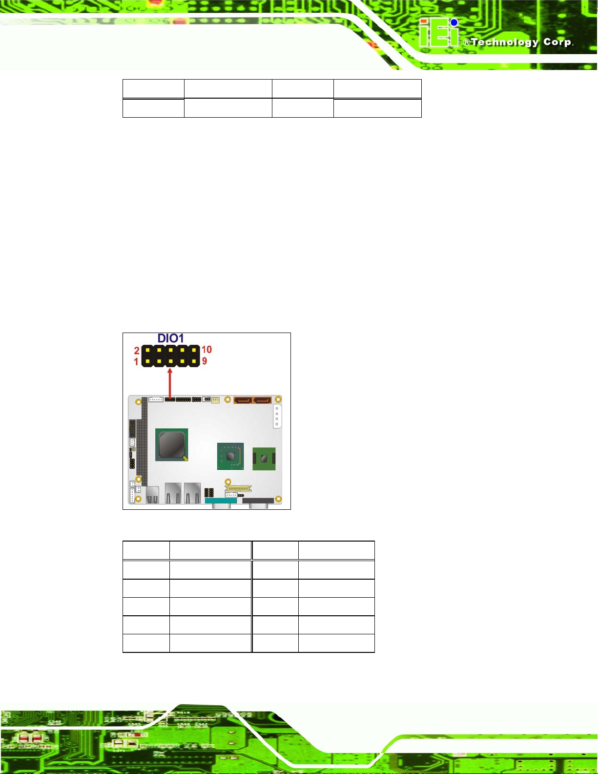
4.3.6 Digital Input/Output (DIO) Connector
CN Label: DIO1
CN Type:
CN Location:
CN Pinouts:
10-pin header (2x5)
Figure 4-8
See
Table 4-8
See
The digital input/output connector is managed through a Super I/O chip. The DIO
connector pins are user programmable.
Figure 4-8: DIO Connector Location
PIN NO. DESCRIPTION PIN NO. DESCRIPTION
1 GND 2 VCC
3 Output 3 4 Output 2
5 Output 1 6 Output 0
7 Input 3 8 Input 2
9 Input 1 10 Input 0
Table 4-8: DIO Connector Pinouts
Page 41
Page 59

4.3.7 Fan Connector (+12V, 3-pin)
WAFER-945GSE2 User Manual
CN Label:
CN Type:
CN Location:
CN Pinouts:
CPU_FAN1
3-pin header
7Figure 4-9
See
7Table 4-9
See
The cooling fan connector provides a 12V, 500mA current to the cooling fan. The
connector has a "rotation" pin to get rotation signals from fans and notify the system so the
system BIOS can recognize the fan speed. Please note that only specified fans can issue
the rotation signals.
Page 42
Figure 4-9: +12V Fan Connector Location
PIN NO. DESCRIPTION
1 GND
2 +12V
3 Fan Speed Detect
Table 4-9: +12V Fan Connector Pinouts
Page 60

WAFER-945GSE2 User Manual
4.3.8 Keyboard/Mouse Connector
CN Label: KB_MS1
CN Type:
CN Location:
CN Pinouts:
6-pin header (1x6)
Figure 4-10
See
Table 4-10
See
The keyboard and mouse connector can be connected to a standard PS/2 cable or PS/2
Y-cable to add keyboard and mouse functionality to the system.
Figure 4-10: Keyboard/Mouse Connector Location
PIN NO. DESCRIPTION
1 +5V KB DATA
2 MS DATA
3 MS CLK
4 KB DATA
5 KB CLK
6 GROUND
Table 4-10: Keyboard/Mouse Connector Pinouts
Page 43
Page 61

4.3.9 LED Connector
CN Label: LED_C1
WAFER-945GSE2 User Manual
CN Type:
CN Location:
CN Pinouts:
6-pin wafer (1x6)
Figure 4-11
See
Table 4-11
See
The LED connector connects to an HDD indicator LED and a power LED on the system
chassis to inform the user about HDD activity and the power on/off status of the system.
Figure 4-11: LED Connector Locations
PIN NO. DESCRIPTION
1 +5V
2 GND
3 Power LED+
4 Power LED5 HDD LED+
6 HDD LED-
Table 4-11: LED Connector Pinouts
4.3.10 LVDS LCD Connector
LVDS1
30-pin crimp (2x10)
See
Page 44
CN Label:
CN Type:
CN Location:
7Figure 4-12
Page 62

WAFER-945GSE2 User Manual
See
CN Pinouts:
7Table 4-12
The 30-pin LVDS LCD connector can be connected to single channel or dual channel,
24-bit or 36-bit LVDS panel.
Figure 4-12: LVDS LCD Connector Pinout Location
PIN NO. DESCRIPTION PIN NO. DESCRIPTION
1 GND1 2 GND2
3 A_Y0 4 A_Y0#
5 A_Y1 6 A_Y1#
7 A_Y2 8 A_Y2#
9 A_CK 10 A_CK#
11 NC 12 NC
13 GND3 14 GND4
15 B_Y0 16 B_Y0#
17 B_Y1 18 B_Y1#
19 B_Y2 20 B_Y2#
21 B_CK 22 B_CK#
23 NC 24 NC
25 GND5 26 GND6
27 VCC_LCD 28 VCC_LCD
29 VCC_LCD 30 VCC_LCD
Table 4-12: LVDS LCD Port Connector Pinouts
Page 45
Page 63

4.3.11 PC/104 Connector
WAFER-945GSE2 User Manual
CN Label:
CN Type:
CN Location:
CN Pinouts:
CN2
104-pin PC/104 slot
7Figure 4-13
See
Table 4-13 and Table 4-14
See
The PCIe mini card slot enables a PCIe mini card expansion module to be connected to
the board. Cards supported include among others wireless LAN (WLAN) cards.
Figure 4-13: PC/104 Connector
PIN Description PIN Description PIN Description PIN Description
A1 -IOCHK A17 SA14 B1 GND B17 -DACK1
A2 SD7 A18 SA13 B2 RSTDRV B18 DRQ1
A3 SD6 A19 SA12 B3 VCC B19 -REFRESH
A4 SD5 A20 SA11 B4 IRQ9 B20 BCLK
A5 SD4 A21 SA10 B5 NC B21 IRQ7
A6 SD3 A22 SA9 B6 DRQ2 B22 IRQ6
A7 SD2 A23 SA8 B7 NC B23 IRQ5
A8 SD1 A24 SA7 B8 -NOWS B24 IRQ4
A9 SD0 A25 SA6 B9 +12V B25 IRQ3
A10 IOCHRDY A26 SA5 B10 GND B26 -DACK2
A11 AEN A27 SA4 B11 -SMEMW B27 TC
Page 46
Page 64

WAFER-945GSE2 User Manual
PIN Description PIN Description PIN Description PIN Description
A12 SA19 A28 SA3 B12 -SMEMR B28 BALE
A13 SA18 A29 SA2 B13 -IOW B29 VCC
A14 SA17 A30 SA1 B14 -IOR B30 ISAOSC
A15 SA16 A31 SA0 B15 -DACK3 B31 GND
A16 SA15 A32 GND B16 DRQ3 B32 GND
Table 4-13: PC/104 Connector Pinouts (1 of 2)
PIN Description PIN Description PIN Description PIN Description
C1 GND C11 -MEMW D1 GND D11 -DACK5
C2 -SBHE C12 SD8 D2 -MEMCS16 D12 DRQ5
C3 SA23 C13 SD9 D3 -IOCS16 D13 -DACK6
C4 SA22 C14 SD10 D4 IRQ10 D14 DRQ6
C5 SA21 C15 SD11 D5 IRQ11 D15 -DACK7
C6 SA20 C16 SD12 D6 IRQ12 D16 DRQ7
C7 SA19 C17 SD13 D7 IRQ15 D17 VCC
C8 SA18 C18 SD14 D8 IRQ14 D18 -MASTER
C9 SA17 C19 SD15 D9 -DACK0 D19 GND
C10 -MEMR C20 NC D10 DRQ0 D20 GND
Table 4-14: PC/104 Connector Pinouts (2 of 2)
4.3.12 PC/104 Power Input Connector
CN Label: CN1
CN Type:
CN Location:
CN Pinouts:
The PC/104 power input connector provides power to the PC/104 expansion module
installed on the PC/104 slot.
3-pin wafer (1x3)
Figure 4-14
See
Table 4-15
See
Page 47
Page 65

Figure 4-14: PC/104 Power Input Connector Pinouts
WAFER-945GSE2 User Manual
PIN NO. DESCRIPTION
1 -5V
2 GND
3 -12V
Table 4-15: PC/104 Power Input Connector Pinouts
4.3.13 Power Button Connector
CN Label: PWRBTN1
CN Type:
CN Location:
CN Pinouts:
The power button connector is connected to a power switch on the system chassis to
enable users to turn the system on and off.
2-pin wafer (1x2)
Figure 4-15
See
Table 4-16
See
Figure 4-15: Power Button Connector Location
Page 48
Page 66

WAFER-945GSE2 User Manual
PIN NO. DESCRIPTION
1 Power Switch
2 GND
Table 4-16: Power Button Connector Pinouts
4.3.14 Reset Button Connector
CN Label: RESET1
CN Type:
CN Location:
CN Pinouts:
The reset button connector is connected to a reset switch o n the syst em chassi s to enabl e
users to reboot the system when the system is turned on.
Figure 4-16: Reset Button Connector Locations
2-pin wafer (1x2)
Figure 4-16
See
Table 4-17
See
PIN NO. DESCRIPTION
1 Reset Switch
2 GND
Table 4-17: Reset Button Connector Pinouts
Page 49
Page 67

4.3.15 SATA Drive Connect ors
WAFER-945GSE2 User Manual
CN Label:
CN Type:
CN Location:
CN Pinouts:
SATA1, SATA2
7-pin SATA drive connectors
8Figure 4-17
See
8Table 4-18
See
The four SATA drive connectors are each connected to a first generation SATA drive. First
generation SATA drives transfer data at speeds as high as 150Mb/s. The SATA drives can
be configured in a RAID configuration.
Page 50
Figure 4-17: SATA Drive Connector Locations
PIN NO. DESCRIPTION
1 GND
2 TX+
3 TX4 GND
5 RX6 RX+
7 GND
Table 4-18: SATA Drive Connector Pinouts
Page 68

WAFER-945GSE2 User Manual
4.3.16 Serial Port Connector (COM2 ) (RS-232, RS-422 or RS-485)
CN Label: COM2
CN Type:
CN Location:
CN Pinouts:
14-pin header (2x7)
Figure 4-18
See
Table 4-19
See
The 14-pin serial port connector connects to the COM2 serial communications channels.
COM2 is a multifunction channel. In default mode COM2 is an RS-232 serial
communication channel but, with the COM2 function select jumper, can be configured as
either an RS-422 or RS-485 serial communications channel.
Figure 4-18: COM2 Connector Pinout Locations
PIN NO. DESCRIPTION PIN NO. DESCRIPTION
1 DATA CARRIER DETECT (DCD) 2 DATA SET READY (DSR)
3 RECEIVE DATA (RXD) 4 REQUEST TO SEND (RTS)
5 TRANSMIT DATA (TXD) 6 CLEAR TO SEND (CTS)
7 DATA TERMINAL READY (DTR) 8 RING INDICATOR (RI)
9 GND 10 N/C
11 TXD485+ 12 TXD485#
13 RXD485+ 14 RXD485#
Table 4-19: COM2 Connector Pinouts
Page 51
Page 69

4.3.17 USB Connectors (Internal)
WAFER-945GSE2 User Manual
CN Label:
CN Type:
CN Location:
CN Pinouts:
USB01 and USB23
8-pin header (2x4)
8Figure 4-19
See
8Table 4-20
See
The 2x4 USB pin connectors each provide connectivity to two USB 1.1 or two USB 2.0
ports. Each USB connector can support two USB devices. Additional external USB ports
are found on the rear panel. The USB ports are used for I/O bus expansion.
Page 52
Figure 4-19: USB Connector Pinout Locations
PIN NO. DESCRIPTION PIN NO. DESCRIPTION
1 VCC 2 GND
3 DATA- 4 DATA+
5 DATA+ 6 DATA7 GND 8 VCC
Table 4-20: USB Port Connector Pinouts
Page 70

WAFER-945GSE2 User Manual
4.4 External Peripheral Interface Connector Panel
8Figure 4-20 shows the WAFER-945GSE2 external peripheral interface connector (EPIC)
panel. The WAFER-945GSE2 EPIC panel consists of the following:
2 x RJ-45 LAN connectors
1 x Serial port connectors
2 x USB connectors
1 x VGA connector
Figure 4-20: WAFER-945GSE2 External Peripheral Interface Connector
4.4.1 LAN Connectors
CN Label:
CN Type:
CN Location:
CN Pinouts:
The WAFER-945GSE2 is equipped with two built-in RJ-45 Ethernet controllers. The
controllers can connect to the LAN through two RJ-45 LAN connectors. There are two
LEDs on the connector indicating the status of LAN. The pin assignments are listed in the
following table:
PIN DESCRIPTION PIN
LAN1 and LAN2
RJ-45
8Figure 4-20
See
8Table 4-21
See
DESCRIPTION
1 MDIA3- 5 MDIA1+
2 MDIA3+ 6 MDIA2+
3 MDIA2- 7 MDIA0-
Page 53
Page 71

4 MDIA1- 8 MDIA0+
WAFER-945GSE2 User Manual
Table 4-21: LAN Pinouts
Figure 4-21: RJ-45 Ethernet Connector
The RJ-45 Ethernet connector has two status LEDs, one green and one yello w. The green
LED indicates activity on the port and the yellow LED indicates the port is linked. See
8Table 4-22.
STATUS
GREEN Activity YELLOW Linked
DESCRIPTION STATUS DESCRIPTION
Table 4-22: RJ-45 Ethernet Connector LEDs
4.4.2 Serial Port Connector (COM1)
CN Label:
CN Type:
CN Location:
CN Pinouts:
The 9-pin DB-9 serial port connectors are connected to RS-232 serial communications
devices.
PIN NO. DESCRIPTION PIN NO. DESCRIPTION
1 DCD 6 DSR
COM1
DB-9 connectors
8Figure 4-20 (see 2)
See
8Table 4-23 and 8Figure 4-22
See
2 RX 7 RTS
3 TX 8 CTS
4 DTR 9 RI
5 GND
Page 54
Page 72

WAFER-945GSE2 User Manual
Table 4-23: RS-232 Serial Port (COM 1) Pinouts
Figure 4-22: COM1 Pinout Locations
4.4.3 USB Connectors
CN Label:
CN T ype:
CN Location:
CN Pinouts:
USB
Dual USB port
8Figure 4-20
See
8Table 4-24
See
The WAFER-945GSE2 has two external USB 2.0 ports. The ports connect to both USB
2.0 and USB 1.1 devices.
PIN NO. DESCRIPTION PIN NO. DESCRIPTION
1 VCC 5 VCC
2 DATA- 6 DATA3 DATA+ 7 DATA+
4 GND 8 GND
Table 4-24: USB Port Pinouts
4.4.4 VGA Connector
CN Label:
CN Type:
CN Location:
CN Pinouts:
VGA1
15-pin Female
8Figure 4-20
See
8Figure 4-23 and 8Table 4-25
See
Page 55
Page 73

WAFER-945GSE2 User Manual
The WAFER-945GSE2 has a single 15-pin female connector for connectivity to standard
display devices.
Figure 4-23: VGA Connector
PIN DESCRIPTION PIN DESCRIPTION
1 RED 2 GREEN
3 BLUE 4 NC
5 GND 6 CRT_PLUG7 GND 8 GND
9 VCC 10 GND
11 NC 12 DDC DAT
13 HSYNC 14 VSYNC
15 DDCCLK
Table 4-25: VGA Connector Pinouts
Page 56
Page 74

WAFER-945GSE2 User Manual
Chapter
5
5 Installation
Page 57
Page 75

5.1 Anti-static Precautions
WARNING:
Failure to take ESD precautions during the installation of the
WAFER-945GSE2 may result in permanent damage to the
WAFER-945GSE2 and severe injury to the user.
Electrostatic discharge (ESD) can cause serious damage to electronic components,
including the WAFER-945GSE2. Dry climates are especially susceptible to ESD. It is
therefore critical to strictly adhere to the following anti-static precautions whenever the
WAFER-945GSE2, or any other electrical component, is handled.
Wear an anti-static wristband: Wearing a simple anti-static wristband can
WAFER-945GSE2 User Manual
help to prevent ESD from damaging the board.
Self-grounding: Before handling the board touch any grounded conducting
material. During the time the board is handled, frequently touch any
conducting materials that are connected to the ground.
Use an anti-static pad: When configuring the WAFER-945GSE2, place it on
an antic-static pad. This reduces the possibility of ESD damaging the
WAFER-945GSE2.
Only handle the edges of the PCB: When handling the PCB, hold the PCB
by the edges.
Installation Considerations
NOTE:
The following installation notices and installation considerations should
be read and understood before the WAFER-945GSE2 is installed. All
installation notices should be strictly adhered to. Failing to adhere to
these precautions may lead to severe damage of the
WAFER-945GSE2 and injury to the person installing the motherboard.
Page 58
Page 76

WAFER-945GSE2 User Manual
5.1.1 Installation Notices
WARNING:
The installation instructions described in this manual should be carefully
followed in order to prevent damage to the WAFER-945GSE2,
WAFER-945GSE2 components and injury to the user.
Before and during the installation please DO the following:
Read the user manual:
o The user manual provides a complete description of the
WAFER-945GSE2 installation instructions and configuration options.
Wear an electrostatic discharge cuff (ESD):
o Electronic components are easily damaged by ESD. Wearing an ESD cuff
removes ESD from the body and helps prevent ESD damage.
Place the WAFER-945GSE2 on an antistatic pad:
o When installing or configuring the motherboard, place it on an antistatic
pad. This helps to prevent potential ESD damage.
Turn all power to the WAFER-945GSE2 off:
o When working with the WAFER-945GSE2, make sure that it is
disconnected from all power supplies and that no electricity is being fed into
the system.
Before and during the installation of the WAFER-945GSE2 DO NOT:
Remove any of the stickers on the PCB board. These stickers are required for
warranty validation.
Use the product before verifying all the cables and power connectors are
properly connected.
Allow screws to come in contact with the PCB circuit, connector pins, or its
components.
Page 59
Page 77

5.1.2 Installation Checklist
The following checklist is provided to ensure the WAFER-945GSE2 is properly installed.
All the items in the packing list are present
A compatible memory module is properly inserted into the slot
The CF Type I or CF Type II card is properly installed into the CF socket
The jumpers have been properly configured
The WAFER-945GSE2 is inserted into a chassis with adequate ventilation
The correct power supply is being used
The following devices are properly connected
o SATA drives
o Power supply
o USB cable
o Serial port cable
WAFER-945GSE2 User Manual
o Keyboard and mouse cable
The following external peripheral devices are properly connected to the
chassis:
o RS-232 serial communications device
o VGA screen
o USB devices
5.2 Unpacking
When the WAFER-945GSE2 is unpacked, please check all the unpacking list items listed
in Chapter 3 are indeed present. If any of the unpacking list items are not available please
contact the WAFER-945GSE2 vendor reseller/vendor where the WAFER-945GSE2 was
purchased or contact an IEI sales representative.
5.3 CF Card Installation
5.3.1 CF Card Installation
NOTE:
The WAFER-945GSE2 can support both CF Type I cards and CF Type
Page 60
Page 78

WAFER-945GSE2 User Manual
II cards. For the complete specifications of the supported CF cards
please refer to Chapter 2.
To install a CF card (Type 1 or Type 2) onto the WAFER-945GSE2, please follow the
steps below:
Step 1: Locate the CF card socket. Place the WAFER-945GSE2 on an anti-static pad
with the solder side facing up. Locate the CF card.
Step 2: Align the CF card. Make sure the CF card is properly aligned with the CF
socket.
Step 3: Insert the CF card. Gently insert the CF card into the socket making sure the
socket pins are properly inserted into the socket. See
Figure 5-1. Step 0:
Figure 5-1: CF Card Installation
Page 61
Page 79

5.4 Jumper Settings
NOTE:
A jumper is a metal bridge used to close an
electrical circuit. It consists of two or three metal
pins and a small metal clip (often protected by a
plastic cover) that slides over the pins to connect
them. To CLOSE/SHORT a jumper means
connecting the pins of the jumper with the plastic
clip and to OPEN a jumper means removing the
WAFER-945GSE2 User Manual
plastic clip from a jumper.
Before the WAFER-945GSE2 is installed in the system, the jumpers must be set in
accordance with the desired configuration. The jumpers on the WAFER-945GSE2 are
listed in
Description Label Type
AT/ATX power mode setting ATXCTL1 3-pin header
CF card setting JCF1 2-pin header
Clear CMOS setup J_CMOS1 3-pin header
COM2 mode setting JP1 8-pin header
LVDS1 voltage select J_VLVDS1 3-pin header
Table 5-1: Jumpers
8Table 5-1.
Figure 5-2: Jumper Locations
5.4.1 AT/ATX Power Select Jumper Settings
NOTE:
The AT Power Select Jumper is the same as the ATX Enable
connector.
Page 62
Page 80

WAFER-945GSE2 User Manual
Jumper Label: ATXCTl1
Jumper Type:
Jumper Settings:
Jumper Location:
3-pin header
Table 5-2
See
Figure 5-3
See
The AT/ATX Power Select jumper specifies the systems power mode as AT or A TX. Use a
jumper cap to short pin 1 - pin 2 on the ATXCTL1 connector to enable the AT Power mode
on the system. In the ATX mode use the PS_ON- and 5VSB cable. AT/ATX Power Select
jumper settings are shown in
AT Power Select Description
Short 2 – 3 Use AT power Default
OFF Use ATX power
Table 5-2.
Table 5-2: AT/ATX Power Select Jumper Settings
The location of the AT Power Select jumper is shown in Figure 5-3 below.
Figure 5-3: AT/ATX Power Select Jumper Location
Page 63
Page 81

5.4.2 CF Card Setup
WAFER-945GSE2 User Manual
Jumper Label:
Jumper Type:
Jumper Settings:
Jumper Location:
JCF1
2-pin header
Table 5-3
See
Figure 5-4
See
The CF Card Setup jumper sets the CF Type I card or CF Type II cards as either the slave
device or the master device. CF Card Setup jumper settings are shown in
CF Card Setup Description
OFF Slave Default
Short 1-2 Master
Table 5-3.
Table 5-3: CF Card Setup Jumper Settings
The CF Card Setup jumper location is shown in Figure 5-4.
Figure 5-4: CF Card Setup Jumper Location
5.4.3 Clear CMOS Jumper
Jumper Label:
Jumper Type:
Jumper Settings:
Jumper Location:
Page 64
J_CMOS1
3-pin header
8Table 5-4
See
8Figure 5-5
See
Page 82

WAFER-945GSE2 User Manual
If the WAFER-945GSE2 fails to boot due to improper BIOS settings, the clear CMOS
jumper clears the CMOS data and resets the system BIOS information. To do this, use the
jumper cap to close pins 2 and 3 for a few seconds then reinstall the jumper clip back to
pins 1 and 2.
If the “CMOS Settings Wrong” message is displayed during the boot up process, the fault
may be corrected by pressing the F1 to enter the CMOS Setup menu. Do one of the
following:
Enter the correct CMOS setting
Load Optimal Defaults
Load Failsafe Defaults.
After having done one of the above, save the changes and exit the CMOS Setup menu.
The clear CMOS jumper settings are shown in
AT Power Select Description
Short 1 - 2 Keep CMOS Setup Default
Short 2 - 3 Clear CMOS Setup
8Table 5-4.
Table 5-4: Clear CMOS Jumper Settings
The location of the clear CMOS jumper is shown in 8Figure 5-5 below.
Page 65
Page 83

Figure 5-5: Clear CMOS Jumper
5.4.4 COM 2 Function Select Jumper
Jumper Label: JP1
WAFER-945GSE2 User Manual
Jumper Type:
Jumper Settings:
Jumper Location:
8-pin header
Table 5-5
See
Figure 5-6
See
The COM 2 Function Select jumper sets the communication protocol used by the second
serial communications port (COM 2) as RS-232, RS-422 or RS -485. The COM 2 Function
Select settings are shown in
COM 2 Function Select Description
Short 1-2 RS-232 Default
Short 3-4 RS-422
Short 5-6 RS-485
Short 5-6
Short 7-8
Table 5-5.
RS-485 with RTS control
Table 5-5: COM 2 Function Select Jumper Settings
The COM 2 Function Select jumper location is shown in Figure 5-6.
Page 66
Page 84

WAFER-945GSE2 User Manual
Figure 5-6: COM 2 Function Select Jumper Location
5.4.5 LVDS Voltage Selection
WARNING:
Permanent damage to the screen and WAFER-945GSE2 may occur if
the wrong voltage is selected with this jumper. Please refer to the user
guide that cam with the monitor to select the correct voltage.
Jumper Label: J_VLVDS1
Jumper Type:
Jumper Settings:
Jumper Location:
The LVDS Voltage Selection jumpers allow the LVDS screen voltages to be set.
J_VLVDS1 sets the voltage connected to LVDS1 and J_VLVDS2 sets the voltage for the
screen connected to LVDS2. The LVDS Voltage Selection jumper settings are shown in
Table 5-6.
3-pin header
Table 5-6
See
Figure 5-7
See
Page 67
Page 85

LCD Voltage Select Description
Short 1-2 +3.3V LVDS Default
Short 2-3 +5V LVDS
Table 5-6: LVDS Voltage Selection Jumper Settings
The LVDS Voltage Selection jumper location is shown in Figure 5-7.
WAFER-945GSE2 User Manual
Figure 5-7: LVDS Voltage Selection Jumper Pinout Locations
5.5 Chassis Installation
5.5.1 Airflow
WARNING:
Airflow is critical to the cooling of the CPU and other onboard
components. The chassis in which the WAFER-945GSE2 must have
air vents to allow cool air to move into the system and hot air to move
out.
The WAFER-945GSE2 must be installed in a chassis with ventilation holes on the sides
allowing airflow to travel through the heat sink surface. In a system with an individual
Page 68
Page 86

WAFER-945GSE2 User Manual
power supply unit, the cooling fan of a power supply can also help generate airflow
through the board surface.
NOTE:
IEI has a wide range of backplanes available. Please contact your
WAFER-945GSE2 vendor, reseller or an IEI sales representative at
3sales@iei.com.tw or visit the IEI website (3http://www.ieiworld.com.tw)
to find out more about the available chassis.
5.5.2 Motherboard Installation
To install the WAFER-945GSE2 motherboard into the chassis please refer to the
reference material that came with the chassis.
5.6 Internal Peripheral Device Connections
5.6.1 Peripheral Device Cables
The cables listed in 8Table 5-7 are shipped with the WAFER-945GSE2.
Quantity Type
1 Keyboard and Mouse cable
2 SATA drive cable
1 Audio cable
1 RS-232 cable
Table 5-7: IEI Provided Cables
Some optional items that can be purchased separately and installed on the
WAFER-945GSE2 include:
Dual port USB cable
RS-232/422/485 cable
ATX power cable
Page 69
Page 87

SATA power cable
5.6.2 SATA Drive Connection
The WAFER-945GSE2 is shipped with two SATA drive cables. To connect the SATA
drives to the connectors, please follow the steps below.
Step 1: Locate the connectors. The locations of the SATA drive connectors are shown
in Chapter 3.
Step 2: Insert the cable connector. Press the clip on the connector at the end of the
SATA cable and insert the cable connector into the onboard SATA drive
WAFER-945GSE2 User Manual
connector. See
8Figure 5-8.
Figure 5-8: SATA Drive Cable Connection
Step 3: Connect the cable to the SA TA disk. Connect the connector on the other end
of the cable to the connector at the back of the SATA drive. See
Page 70
8Figure 5-9.
Page 88

WAFER-945GSE2 User Manual
NOTE:
The SATA power cable described below is an optional item and must
be pre-ordered. The SATA power cable is not shipped with the system.
Step 4: Connect the SATA power cable. Connect the SATA power connector to the
back of the SATA drive. See
Figure 5-9: SATA Power Drive Connection
8Figure 5-9. Step 0:
5.6.3 Dual RS-232 Cable Connection (w/o bracket) (Optional)
The dual RS-232 cable consists of two connectors attached to two independent cables.
Each cable is then attached to a D-sub 9-pin male connector. To install the dual RS-232
cable, please follow the steps below.
Step 1: Locate the connectors. The locations of the RS-232 connectors are shown in
Chapter 3.
Step 2: Insert the cable connectors. Insert one connector into each serial port box
headers. See
Figure 5-10. A key on the front of the cable connectors ensures
Page 71
Page 89

the connector can only be installed in one direction.
Figure 5-10: Dual RS-232 Cable Installation
WAFER-945GSE2 User Manual
Step 3: Secure the connectors. Both single RS-232 connectors have two retention
screws that must be secured to a chassis or bracket.
Step 4: Connect the serial device. Once the single RS-232 connectors are connected
to a chassis or bracket, a serial communications device can be connecte d to the
system. Step 0:
Page 72
Page 90

WAFER-945GSE2 User Manual
Figure 5-11: Serial Device Connector
5.6.4 Keyboard/Mouse Y-cable Connector
The WAFER-945GSE2 is shipped with a keyboard/mouse Y-cable connector. The
keyboard/mouse Y-cable connector connects to a keyboard/mouse connector on the
WAFER-945GSE2 and branches into two cables that are each connected to a PS/2
connector, one for a mouse and one for a keyboard. To connect the keyboard/mouse
Y-cable connector, please follow the steps below.
Step 1: Locate the connector. The location of the keyboard/mouse Y-cable connector
is shown in Chapter 3.
Step 2: Align the connectors. Correctly align pin 1 on the cable connector with pin 1 on
the WAFER-945GSE2 keyboard/mouse connector. See
Step 3: Insert the cable connectors. Once the cable connector is properly aligned with
the keyboard/mouse connector on the WAFER-945GSE2, connect the cable
Figure 5-12.
connector to the on-board connectors. See
Figure 5-12.
Page 73
Page 91

WAFER-945GSE2 User Manual
Figure 5-12: Keyboard/mouse Y-cable Connection
Step 4: Attach PS/2 connectors to the chassis. The keyboard/mouse Y -cabl e
connector is connected to two PS/2 connectors. To secure the PS/2 connectors
to the chassis please refer to the installation instructions that came with the
chassis.
Step 5: Connect the keyboard and mouse. Once the PS/2 connectors are connected
to the chassis, a keyboard and mouse can each be connected to one of the
PS/2 connectors. The keyboard PS/2 connector and mouse PS/2 connector are
both marked. Please make sure the keyboard and mouse are connected to the
correct PS/2 connector. Step 0:
5.6.5 Audio Kit Installation
The Audio Kit that came with the WAFER-945GSE2 connects to the 10-pin audio
connector on the WAFER-945GSE2. The audio kit consists of three audio jacks. One
audio jack, Mic In, connects to a microphone. The remaining two audio jacks, Line-In and
Line-Out, connect to two speakers. To install the audio kit, please refer to the steps b elow:
Page 74
Page 92

WAFER-945GSE2 User Manual
Step 1: Locate the audio connector. The location of the 10-pin audio connector is
shown in Chapter 3.
Step 2: Align pin 1. Align pin 1 on the on-board connector with pin 1 on the audio kit
connector. Pin 1 on the audio kit connector is indicated with a white dot. See
Figure 5-13.
Figure 5-13: Audio Kit Cable Connection
Step 3: Connect the audio devices. Connect one speaker to the line-in audio jack, one
speaker to the line-out audio jack and a microphone to the mic-in audio jack.
5.6.6 PC/104 Module Installation
The WAFER-945GSE2 has a standard PC/104 connector. To install a PC/104 module
please refer to and follow the installation instructions and diagram below:
Page 75
Page 93

WAFER-945GSE2 User Manual
Figure 5-14: WAFER-945GSE2 PC/104 module installation
Step 1: Remove retention nuts. Remove the two nuts securing the heatsink and two
nuts securing the WAFER-945GSE2 to the chassis.
Step 2: Attach intermediate poles. Insert the two short plastic intermediate poles into
the bolts securing the heatsink. Insert the two tall plastic intermediate poles.
Step 3: Align the PC/104 connector. Align the PC/104 module connector with the
corresponding connector on the WAFER-945GSE2 (conne ctor CN2). Gently
push the module down to ensure the connectors are properly connected.
Step 4: Replace the retention nuts. Screw the four retention nuts onto the
intermediate poles to secure the PC/104 module.
5.6.7 USB Cable (Dual Port without Bracket) (Optional)
The WAFER-945GSE2 is shipped with a dual port USB 2.0 cable. To connect the USB
cable connector, please follow the steps below.
Step 5: Locate the connectors. The locations of the USB connectors are shown in
Page 76
Page 94

WAFER-945GSE2 User Manual
Chapter 3.
WARNING:
If the USB pins are not properly aligned, the USB device can burn out.
Step 6: Align the connectors. The cable has two connectors. Correctly align pin 1on
each cable connector with pin 1 on the WAFER-945GSE2 USB connector.
Step 7: Insert the cable connectors. Once the cable connectors are properly aligned
with the USB connectors on the WAFER-945GSE2, connect the cable
connectors to the on-board connectors. See
Figure 5-15: Dual USB Cable Connection
Step 8: Attach the USB connectors to the chassis. The USB 2.0 connectors each of
two retention screw holes. To secure the connectors to the chassis please refer
Figure 5-15.
to the installation instructions that came with the chassis.Step 0:
5.7 External Peripheral Interface Connection
The following external peripheral devices can be connected to the external peripheral
interface connectors.
Page 77
Page 95

RJ-45 Ethernet cable connectors
Serial port devices
USB devices
VGA monitors
To install these devices, connect the corresponding cable connector from the actual
device to the corresponding WAFER-945GSE2 external peripheral interface connector
making sure the pins are properly aligned.
5.7.1 LAN Connection (Single Connector)
There are two external RJ-45 LAN connectors. The RJ-45 connectors enable connection
to an external network. To connect a LAN cable with an RJ-45 connector, please follow
the instructions below.
Step 1: Locate the RJ-45 connectors. The locations of the USB connectors are shown
WAFER-945GSE2 User Manual
in Chapter 4.
Step 2: Align the connectors. Align the RJ-45 connector on the LAN cable with one of
the RJ-45 connectors on the WAFER-945GSE2. See
8Figure 5-16.
Figure 5-16: LAN Connection
Page 78
Page 96

WAFER-945GSE2 User Manual
Step 3: Insert the LAN cable RJ-45 connector. Once aligned, gently insert the LAN
cable RJ-45 connector into the onboard RJ-45 connector. Step 0:
5.7.2 Serial Device Connection
The WAFER-945GSE2 has a single female DB-9 connector on the external peripheral
interface panel for a serial device. Follow the steps below to connect a serial device to the
WAFER-945GSE2.
Step 1: Locate the DB-9 connector. The location of the DB-9 connector is shown in
Chapter 3.
Step 2: Insert the serial connector. Insert the DB-9 connector of a serial device into
the DB-9 connector on the external peripheral interface. See
Figure 5-17: Serial Device Connector
8Figure 5-17.
Step 3: Secure the connector. Secure the serial device connector to the external
interface by tightening the two retention screws on either side of the connector.
Step 0:
Page 79
Page 97

5.7.3 USB Connection (Dual Connector)
The external USB receptacle connectors provide easier and quicker access to external
USB devices. Follow the steps below to connect USB devices to the WAFER-945GSE2.
Step 1: Locate the USB receptacle connectors. The location of the USB receptacle
connectors are shown in Chapter 3.
Step 2: Insert a USB plug. Insert the USB plug of a device into the USB receptacle on
WAFER-945GSE2 User Manual
the external peripheral interface. See
Figure 5-18: USB Connector
8Figure 5-18.Step 0:
5.7.4 VGA Monitor Connection
The WAFER-945GSE2 has a single female DB-15 connector on the external peripheral
interface panel. The DB-15 connector is connected to a CRT or VGA monitor. To connect
a monitor to the WAFER-945GSE2, please follow the instructions below.
Step 1: Locate the female DB-15 connector. The location of the female DB-15
connector is shown in Chapter 3.
Page 80
Page 98

WAFER-945GSE2 User Manual
Step 2: Align the VGA connector. Align the male DB-15 conn ector on the VGA screen
cable with the female DB-15 connector on the external peripheral interface.
Step 3: Insert the VGA connector. Once the connectors are properly aligned with the
insert the male connector from the VGA screen into the female connector on the
WAFER-945GSE2. See
Figure 5-19: VGA Connector
8Figure 5-19.
Step 4: Secure the connector. Secure the DB-15 VGA connector from the VGA
monitor to the external interface by tightening the two retention screws on either
side of the connector. Step 0:
Page 81
Page 99

WAFER-945GSE2 User Manual
Chapter
6
6 BIOS Screens
Page 82
Page 100

WAFER-945GSE2 User Manual
6.1 Introduction
A licensed copy of AMI BIOS is preprogrammed into the ROM BIOS. The BIOS setup
program allows users to modify the basic system configuration. This chapter describes
how to access the BIOS setup program and the configuration options that may be
changed.
6.1.1 Starting Setup
The AMI BIOS is activated when the computer is turned on. The setup program can be
activated in one of two ways.
1. Press the D
2. Press the D
appears on the screen. 0.
If the message disappears before the D
again.
ELETE key as soon as the system is turned on or
ELETE key when the “Press Del to enter SETUP” message
ELETE key is pressed, restart the computer and try
6.1.2 Using Setup
Use the arrow keys to highlight items, press ENTER to select, use the PageUp and
PageDown keys to change entries, press F1 for help and press E
keys are shown below.
Key Function
Up arrow Move to previous item
Down arrow Move to next item
Left arrow Move to the item on the left hand side
SC to quit. Navigation
Right arrow Move to the item on the right hand side
Esc key Main Menu – Quit and not save changes into CMOS
Status Page Setup Menu and Option Page Setup Menu --
Exit current page and return to Main Menu
Page Up key Increase the numeric value or make changes
Page Dn key Decrease the numeric value or make changes
Page 83
 Loading...