Page 1

I
WAFER-6820
Low Power Transmeta TM3200 400MHZ
With CRT/LCD, Ethernet
Single Board Computer
Copyright Notice
©Copyright 2000 by ICP Electronics Inc. All Rights Reserved. Manual first edition
Nov.01, 2000.
The information in this document is subject to change without prior notice in order
to improve reliability, design and function and does not represent a commitment on
the part of the manufacturer.
In no event will the manufacturer be liable for direct, indirect, special, incidental, or
consequential damages arising out of the use or inability to use the product or
documentation, even if advised of the possibility of such damages.
This document contains proprietary information protected by copyright. All rights
are reserved. No part of this manual may be reproduced by any mechanical,
electronic, or other means in any form without prior written permission of the
manufacturer.
Trademarks
WAFER-6820 is a registered trademark of ICP Electronics Inc. IBM PC is a
registered trademark of International Business Machines Corporation. Intel is a
registered trademark of Intel Corporation. Other product names mentioned herein
are used for identification purposes only and may be trademarks and/or registered
trademarks of their respective companies.www.iei.com.tw
Page 2

II
Contents
Contents................................................................... II
1 Introduction................................................................1
1.1 Specifications: .................................................................................2
1.2 What You Have ...............................................................................4
2 Installation..................................................................5
2.1 WAFER-6820 Layout ......................................................................5
2.2 WAFER-6820 DIMENSION............................................................7
2.3 Unpacking.......................................................................................8
2.4 Clear CMOS Setup (J2) ...................................................................9
2.5 Fan Connector (J3) ..........................................................................9
2.6 LCD Voltage and Clock Setting (J4)................................................9
2.7 Buzzer Setting (J5-Pin 1,2)............................................................10
2.8 Compact Flash Setting (J5-Pin 3,4)................................................10
2.9 COM2 PIN8 Setting (J6)................................................................10
2.10 COM2 RS-232, RS-422 or RS-485 Setting (J7)............................11
2.11 Watchdog Timer Setting (J8).......................................................11
2.12 Reset Button (J9) .........................................................................11
3 Connection...............................................................12
Page 3

III
3.1 External Power Connector (CN1)...................................................12
3.2 PC/104 Connection Bus (CN2, CN3).............................................12
3.3 LAN RJ45 Connector (CN4)..........................................................14
3.4 LCD Interface Connector (CN5)....................................................15
3.5 IDE Disk Drive Connector (CN6)..................................................17
3.6 CompactFlash Connector -- TYPE II (CN7)...................................18
3.7 IrDA Infrared Interface Port (CN8)................................................19
3.8 Keyboard Connector (CN9)............................................................19
3.9 Floppy Disk Drive Connector (CN10)............................................20
3.10 USB Port Connector (CN12)........................................................20
3.11 Parallel Port (CN13)....................................................................21
3.12 Serial Ports (CN14, CN15) ..........................................................21
3.13 Audio Connector (CN16, CN17)..................................................22
3.14 VGA Connector (CN18) ..............................................................23
3.15 TV-OUTPUT Connector (CN19) (Optional) ................................24
4 AWARD BIOS Setup...............................................25
4.1 Introduction...................................................................................25
4.2 Starting Setup................................................................................25
4.3 Using Setup...................................................................................26
4.4 Main Menu....................................................................................27
4.5 Standard CMOS Setup...................................................................30
4.6 Advanced BIOS Features...............................................................35
Page 4

IV
4.7 Integrated Peripherals....................................................................39
4.8 Power Management Setup..............................................................43
4.9 PnP/PCI Configuration Setup.........................................................47
4.10 PC Health Status..........................................................................49
4.11 Defaults Menu .............................................................................50
4.12 Supervisor/User Password Setting................................................51
4.13 Exit Selecting ..............................................................................52
Appendix A. Watch-Dog Timer.................................53
Appendix B. I/O Address Map...................................55
B.1 System I/O Address Map...............................................................55
B.2 DMA channel assignments............................................................56
B.3 Interrupt assignments....................................................................57
B.4 1st MB memory map......................................................................57
Page 5

1
1
Introduction
WAFER-6820 is designed for limited space applications with only the
size of a 3½" hard drive. It supports the full functions of an AT-compatible
industrial computer on a single board. The WAFER-6820 is equipped with a
low-power consumption and high performance Transmeta TM3200
processor on board. It also contains an SDRAM SODIMM socket that can
support up to 128MB memory.
The WAFER-6820 provides an Ethernet interface, audio interface,
Compact Flash Type II, EIDE interface, one parallel port, one serial port
RS-232, one serial port RS-232/422/485 with auto-direction, and a mini-DIN
PS/2 keyboard/mouse interface. The built-in SVGA/LCD display controller
supports both the CRT and LCD display simultaneously. It offers the
resolutions of LCD screen up to 1024 x 768 and CRT resolutions up to 1280
x 1024 @ 16 colors. The display type is configured by software utility. The
Flash ROM contains both the system BIOS and the VGA BIOS.
Reprogramming the Flash ROM could do the modification, in case of
necessary.
The RS485 has an outstanding characteristic of intelligent directing
control, which eliminates the extra control signal like RTS. With this feature
you can develop your program as you are using a normal RS232 without
special control routine. This is especially important in WINDOWS
programming which do not allow the program to catch the control pin at
Page 6

2
your wish.
Finally, one PC/104 connector is included for the future application you
will need.
Notes:
The Transmeta Crusoe™ TM3200 will occupy 16MB memory space to
save its CMS code temporally. So we must indicate the memory type for
Tramsmeta Crusoe™ TM3200. Because this point, we will attaché one
128MB SDRAM module that we approved in the package.
1.1 Specifications:
The WAFER-6820 TM3200 with VGA Computer provides the
following specification:
•
CPU: Low power Transmeta Crusoe ™TM3200 400 MHz
•
Bus
: ISA bus
•
DMA channels: 7
•
Interrupt levels: 15
•
Chipset: TM3200 + VIA VT82C686A
•
PCI VGA: C&T 69000 with 2MB SDRAM built-in Chipset
Resolution: 1280x1024, 256 color, 60Hz
1024x768, 64K color, 85Hz
800x600,full color, 85Hz
•
Ethernet Interface:
Chipset: Realtek 8139C 100Base-TX Fast Ethernet Controller
Ethernet Interface: Onboard 100Base-TX RJ-45+LED Connector
•
H/W status Monitoring: VT82C686A H/W status monitoring
IC supports power supply voltages and temperatures monitoring
•
Real-Time Clock/Calendar: built-in VT82C686A chipset, backup by
industrial Li-battery, 3V/300mAH. .
•
DRAM: supports to 128MB,SDRAM.
Page 7

3
•
Ultra DMA/33 IDE Interface: supports up to two PCI Enhance IDE hard
drives. The Ultra DMA/33 IDE can handle data transfer up to 33MB/s.
The best of all is that it is compatible with existing ATA-2 IDE
specifications. So there is no need to do any change for customer’s
current accessory.
•
Floppy disk drive interface: two 2.88 MB, 1.44MB, 1.2MB, 720KB, or
360KB floppy disk drives.
•
Two high-speed Serial ports: NS16C550 compatible UARTs, and one
RS422/485 port with auto-direction function.
•
Bi-directional Parallel Port: IEEE 1284 compatible
•
IrDA port: Support serial Infrared (SIR).
•
USB port: Support two USB ports for future expansion, USB 1.1
compliant.
• Watchdog timer
•
CompactFlash disk: The CompactFlash Storage Card also runs in
True IDE Mode that is compatible with an IDE disk drive. It can be used
with a passive adapter in a Type II socket.
•
Keyboard connector
•
Mouse: PS/2 Mouse Port on-board.
•
Power Consumption: +5V @ 1.8A
(Transmeta TM3200, 128MB SDRAM)
•
Operating Temperature
: 0° ~ 60°C (CPU needs heat sink)
Page 8

4
1.2 What You Have
Before you install the product, please check the following materials are
included in the package:
• 1 WAFER-6820 All-in-one single board computer
• 1 CD disk for utility and drivers
• 1 3.5" IDE flat cable (44-pin 2.0mm pitch to 40-pin 2.54mm pitch)
• 1 one to two 6pin mini Din connector for keyboard and mouse
• 1 combo serial port cable (RS-232/422/485)
• 1 standard D25 connector for parallel cable
• 1 floppy cable (for 3.5" FDD only)
If any of these items are missing or damaged, contact your distributor
or sales representative immediately.
Page 9

5
2
Installation
This chapter describes how to install the WAFER-6820. At first, the
layout of WAFER-6820 is shown, and the unpacking information
that you should be careful is described. The jumpers and switches
setting for the WAFER-6820's configuration, such as watchdog
timer, are also included.
2.1 WAFER-6820 Layout
(Please refer to next page)
Page 10

6
Page 11

7
2.2 WAFER-6820 DIMENSION
Page 12

8
2.3 Unpacking
Your WAFER-6820 Single Board Computer contains sensitive
electronic components that can be easily damaged by static
electricity.
In this section, we describe the precautions you should take while
unpacking, as well as during installation. It is very important that the
instructions be followed correctly, to avoid static damage, and to
successfully install the board.
The system board should be done on a grounded anti-static mat.
The operator should be wearing an anti-static wristband, grounded
at the same point as the anti-static mat.
Inspect the cardboard carton for obvious damage. Shipping and
handling may cause damage to your board. Be sure there are no
shipping and handing damages on the board before processing.
After opening the cardboard carton, exact the system board and
place it only on a grounded anti-static surface component side up.
Again inspect the board for damage. Press down on all the
docketed IC's to make sure that they are properly seated.
Do this only with the board place on a firm flat surface.
Note: DO NOT APPLY POWER TO THE BOARD IF IT HAS BEEN
DAMAGED.
You are now ready to install your WAFER-6820 Single Board
Computer.
Page 13

9
2.4 Clear CMOS Setup (J2)
If want to clear the CMOS Setup (for example forgot the password you
should clear the setup and then set the password again.), you should
close the J2 pin 2-3 about 3 seconds, then open again. Set back to
normal operation mode, close pin 1-2.
J2 DESCRIPTION
1-2 Normal Operation
2-3
Clear CMOS Setup
2.5 Fan Connector (J3)
The WAFER-6820 provides a CPU cooling fan connector. This
connector can supply 5V/500mA to the cooling fan.
PIN NO. DESCRIPTION
1 +5V
2 GND
2.6 LCD Voltage and Clock Setting (J4)
The LCD interface connector CN5 can provide 5V or 3.3V power
supply by selecting the J4 (2,4,6) to meet the different LCD
requirement. And the JP4 (1,3,5) can provide normal or inverted Shift
CLOCK for LCD.
J4 (2,4,6) DESCRIPTION
2-4 5V
4-6 3.3V
JP4 (1,3,5) DESCRIPTION
1-3 Shift Clock Invert
3-5 Shift Clock (Normal)
Page 14

10
2.7 Buzzer Setting (J5-Pin 1,2)
Set the operating mode of Buzzer.
Address
J5-1, 2
Buzzer ON
CLOSE
Buzzer OFF
OPEN
2.8 Compact Flash Setting (J5-Pin 3,4)
Set the operating mode of CompactFlash disk. This is similar to the
operation of hard disk.
Address
J5-3, 4
MASTER
CLOSE
SLAVE
OPEN
2.9 COM2 PIN8 Setting (J6)
In the RS232 mode
, the COM2 (CN15) can supply +5V or +12V
power to the serial devices via RI pin (Pin 8) of the COM port
connector. The maximal current is 1A with fuse protection, from these
two connector’s 5V/12V output. If the output is set to 12V, make sure
that you have 12V supply to the board.
CN9 Pin 8 J6 (1,3,5)
J6 (2,4,6)
J7
RI Signal 3-5 Don’t care
1-2
+5V
1-3 4-6 1-2
+12V
1-3 2-4 1-2
Page 15

11
2.10 COM2 RS-232, RS-422 or RS-485 Setting (J7)
The COM2 (CN15) can be set to RS-232 or RS-422/485 for industrial
field site application. Moreover when this port was set to the RS-485
mode, the board equipped with auto-direction IC will automatically
sense the data direction to eliminate the data collision. This is
especially important in WINDOWS programming which do not allow
the program to catch the control pin at your wish.
J7 DESCRIPTION
1-2 RS232
3-4 RS422/RS485
2.11 Watchdog Timer Setting (J8)
R reading port 443H enables the Watch-Dog Timer. It should be retriggered before the time-out period ends, otherwise it will assume the
program operation is abnormal and will issue a reset signal to start
again, or activate NMI to CPU. Reading port 043/843H disables the
watchdog Timer. Refer to Appendix A for more detailed information on
Watchdog Timer
J8
DESCRIPTION
1-2
ACTIVATE NMI TO CPU WHEN WDT TIME-OUT
2-3
RESET WHEN WDT TIME-OUT
OPEN
DISABLE WDT
2.12 Reset Button (J9)
You can press Reset Button (J9) to reset your computer easily.
PIN NO. DISCRPTION
1 Reset _In
2 GND
Page 16

12
3
Connection
This chapter describes how to connect peripherals, switches and
indicators to the WAFER-6820 board.
3.1 External Power Connector (CN1)
The WAFER-6820 has an on-board external power connector CN1.
You can apply power directly to the CPU board.
•CN1: External Power Connector
PIN NO. DESCRIPTION
1 +12V
2 GROUND
3 GROUND
4 +5V
3.2 PC/104 Connection Bus (CN2, CN3)
The WAFER-6820 PC/104 expansion bus let you attach any kind of
PC/104 modules. The PC/104 bus has already become the industrial
embedded PC bus standard, so you can easily install over thousands
of PC/104 modules from hundreds of vendors in the world. There are
two PC/104 connectors on this board: PC/104-64 and PC/104-40.
Page 17

13
•CN2: PC/104-64 Connector
PIN NO.
Description PIN NO.
Description
1 IOCHCK# 2 GND
3 SD7 4 IRSTDRV
5 SD6 6 VCC
7 SD5 8 IRQ9
9 SD4 10 -5V
11 SD3 12 N/C
13 SD2 14 -12V
15 SD1 16 ZWS
17 SD0 18 +12V
19 IOCHRDY 20 GND
21 AEN 22 SMEMW#
23 SA19 24 SMEMR#
25 SA18 26 IOW#
27 SA17 28 IOR#
29 SA16 30 DACK3#
31 SA15 32 DRQ3
33 SA14 34 DACK1#
35 SA13 36 DRQ1
37 SA12 38 REFRESH#
39 SA11 40 SYSCLK
41 SA10 42 IRQ7
43 SA9 44 N/C
45 SA8 46 IRQ5
47 SA7 48 IRQ4
49 SA6 50 IRQ3
51 SA5 52 N/C
53 SA4 54 TC
55 SA3 56 BALE
57 SA2 58 VCC
59 SA1 60 OSC
61 SA0 62 GND
63 GND 64 GND
Page 18

14
•
CN3: PC/104-40 Connector
PIN NO.
Description PIN NO
Description
1 GND 2 GND
3 SBHE# 4 MCS16#
5 LA23 6 IOCS16#
7 LA22 8 IRQ10
9 LA21 10 IRQ11
11 LA20 12 IRQ12
13 LA19 14 IRQ15
15 LA18 16 IRQ14
17 LA17 18 DACK0#
19 MEMR# 20 DRQ0
21 MEMW# 22 DACK5#
23 SD8 24 DRQ5
25 SD9 26 DACK6#
27 SD10 28 DRQ6
29 SD11 30 DACK7#
31 SD12 32 DRQ7
33 SD13 34 VCC
35 SD14 36 MASTER#
37 SD15 38 GND
39 GND 40 GND
3.3 LAN RJ45 Connector (CN4)
The WAFER-6820 builds in RJ45 LAN connector. It’s for 10/100Mbps
Ethernet (RTL8139C).
•CN4: LAN RJ45 Connector
1 TX+ 5 NC
2 TX- 6 RX3 RX+ 7 NC
4 NC 8 NC
Page 19

15
3.4 LCD Interface Connector (CN5)
The WAFER-6820 provides a 2x25-pin connector for the LCD flat
panel interface.
The WAFER-6820 comes to support TFT/DSTN LCD panels at
following display options: (This is a reference table only, may support
more type of panels)
Display type Resolution Example
TFT VGA
640X480, 64K Color
12 bits
TFT VGA
640X480, 64K Color,
18bits
P64CV1
TFT SVGA
800X600, 64K Color,
18bits
IMES M121-533DR
TFT XGA
1024X768, 64K Color,
36bits
Sharp LQ150X1DG11
The display options need to be setup from BIOS. The BIOS “Standard
CMOS” Setup allow you to choose display resolution either 640X480,
800X600 or 1024X768.
Page 20

16
• CN5: LCD Interface Connector – supports up to 36-bit LCD. For
better display quality, the length of LCD cable should be shorter
than 45 cm.
PIN NO. Description PIN NO. Description
1 NC 2 P33
3 P34 4 P31
5 P35 6 P32
7 P30 8 P28
9 P29 10 P27
11 P25 12 P26
13 P24 14 P21
15 P23 16 P22
17 P16 18 P20
19 P17 20 P18
21 P19 22 P14
23 P13 24 P12
25 P15 26 P11
27 P7 28 P10
29 FPVCC 30 FPVCC
31 P9 32 P8
33 P4 34 P6
35 P3 36 P5
37 P2 38 P1
39 M 40 P0
41 SHIFT CLOCK
42 ENABKL
43 FPVDD
44 FLM
45 ENAVEE 46 LP
47 GND 48 GND
49 +12V 50 +12V
Page 21

17
3.5 IDE Disk Drive Connector (CN6)
You can attach two IDE (Integrated Device Electronics) hard disk
drives to the WAFER-6820 IDE controller (Primary). The IDE
supports Ultra DMA/33 interface.
PIN NO. DESCRIPTION PIN NO. DESCRIPTION
1 RESET# 2 GROUND
3 DATA 7 4 DATA 8
5 DATA 6 6 DATA 9
7 DATA 5 8 DATA 10
9 DATA 4 10 DATA 11
11 DATA 3 12 DATA 12
13 DATA 2 14 DATA 13
15 DATA 1 16 DATA 14
17 DATA 0 18 DATA 15
19 GROUND 20 N/C
21 N/C 22 GROUND
23 IOW# 24 GROUND
25 IOR# 26 GROUND
27 N/C 28 BALE – DEFAULT
29 N/C 30 GROUND –DEFAULT
31 INTERRUPT 32 IOCS16#-DEFAULT
33 SA1 34 N/C
35 SA0 36 SA2
37 HDC CS0# 38 HDC CS1#
39 HDD ACTIVE# 40 GROUND
41 VCC 42 VCC
43 GROUND 44 N/C
Page 22

18
3.6 CompactFlash Connector -- TYPE II (CN7)
You can attach one Compact Flash Disk to CN7 that occupy the
Secondary IDE channel. The CN7 supports both the TYPE II and
TYPE I module.
• CN7: CompactFlash Connector (Secondary IDE)
PIN NO.
DESCRIPTION PIN NO. DESCRIPTION
1 GROUND 26 VCC-IN CHECK1
2 DATA 3 27 DATA 11
3 DATA 4 28 DATA 12
4 DATA 5 29 DATA 13
5 DATA 6 30 DATA 14
6 DATA 7 31 DATA 15
7 HDC_CS0# 32 HDC_CS1
8 N/C 33 N/C
9 GROUND 34 IOR#
10 N/C 35 IOW#
11 N/C 36 N/C
12 N/C 37 INTERRUPT
13 VCC_COM 38 VCC_COM
14 N/C 39 CSEL
15 N/C 40 N/C
16 N/C 41 HDD_RESET
17 N/C 42 IORDY
18 SA2 43 N/C
19 SA1 44 VCC_COM
20 SA0 45 HDD_ACTIVE#
21 DATA 0 46 N/C
22 DATA 1 47 DATA 8
23 DATA 2 48 DAYA 9
24 N/C 49 DATA 10
25 VCC-IN CHECK2
50 GROUND
Page 23

19
3.7 IrDA Infrared Interface Port (CN8)
The WAFER-6820 builds in an IrDA port, which supports Serial Infrared
(SIR). Using the IrDA port has to set the mode of COM2 as SIR (in the
BIOS’s Peripheral Setup’s). Then the RS-232mode of COM2 will be
disabled.
•
CN8: IrDA connector
PIN NO. DISCRPTION
1 VCC
2 N/C
3 IRRX
4 Ground
5 IRTX
3.8 Keyboard Connector (CN9)
The WAFER-6820 provides one external keyboard and one PS/2
Keyboard and mouse connectors.
•
CN9: 6-pin Mini-DIN Keyboard and Mouse Connector
PIN NO. DESCRIPTION
1 KB DATA
2 MS DATA
3 GND
4 +5V
5 KB CLOCK
6 MS CLOCK
Page 24
20
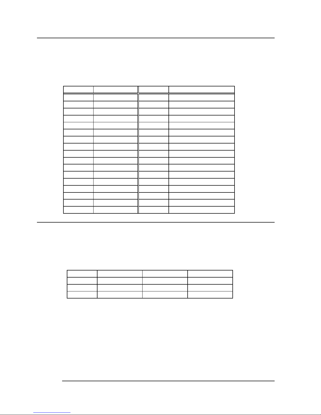
3.9 Floppy Disk Drive Connector (CN10)
The WAFER-6820 board is equipped with a 34-pin daisy-chain
driver connector cable.
•
CN10: FDC CONNECTOR (2.0MM)
PIN NO. DESCRIPTION
PIN NO. DESCRIPTION
1 GROUND 2 REDUCE WRITE
3 GROUND 4 N/C
5 N/C 6 DRVDEN1
7 GROUND 8 INDEX#
9 GROUND 10 MOTOR ENABLE A#
11 GROUND 12 DRIVE SELECT B#
13 GROUND 14 DRIVE SELECT A#
15 GROUND 16 MOTOR ENABLE B#
17 GROUND 18 DIRECTION#
19 GROUND 20 STEP#
21 GROUND 22 WRITE DATA#
23 GROUND 24 WRITE GATE#
25 GROUND 26 TRACK 0#
27 GROUND 28 WRITE PROTECT#
29 GROUND 30 READ DATA#
31 GROUND 32 SIDE 1 SELECT#
33 GROUND 34 DISK CHANGE#
3.10 USB Port Connector (CN12)
The WAFER-6820 builds in two USB ports for the future new I/O
bus expansion. It is USB 1.1 compliant
•CN12: USB 0 & USB 1
1 VCC 5 GROUND
2 DATA0- 6 DATA1+
3 DATA0+ 7 DATA14 GROUND 8 VCC
Page 25
21
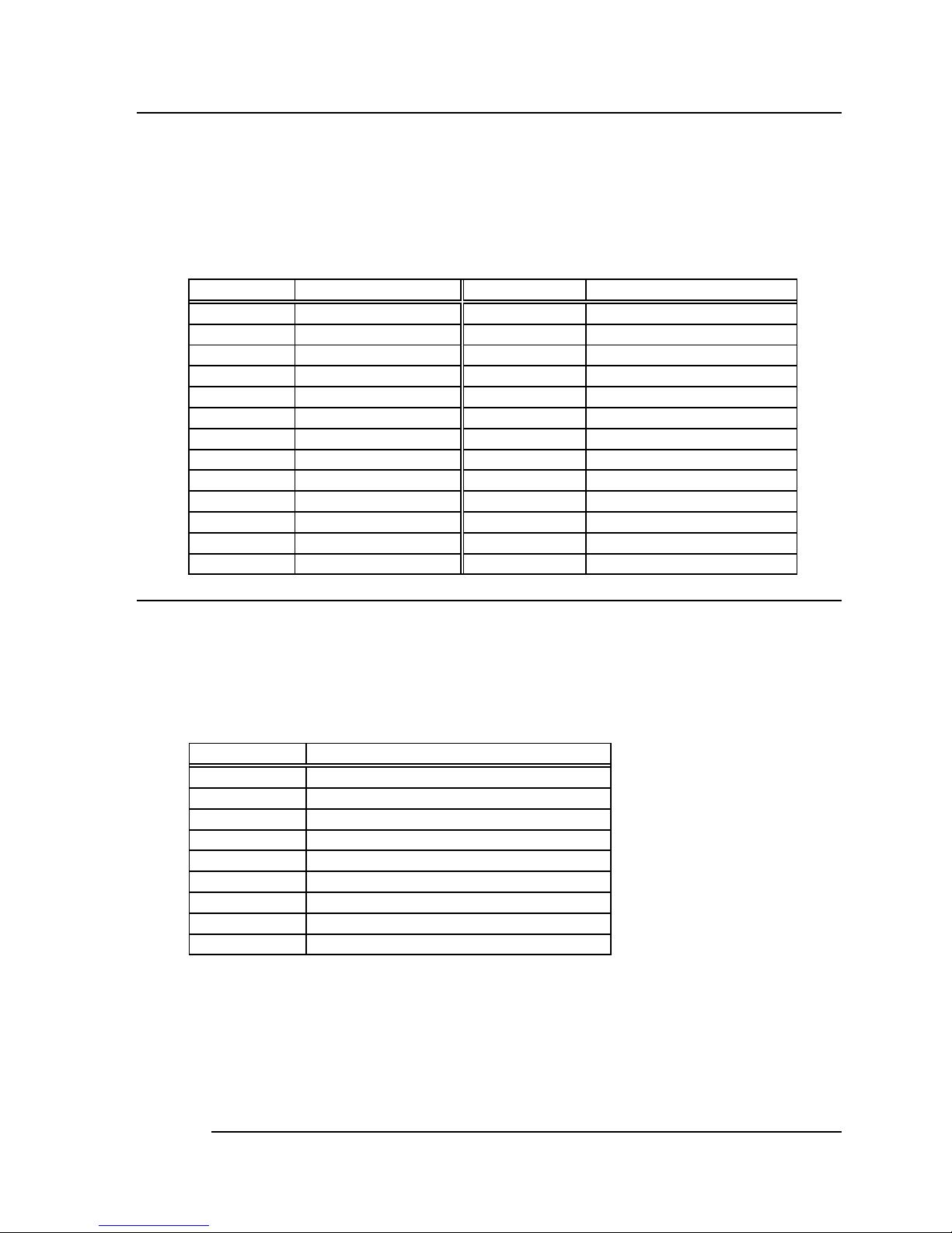
3.11 Parallel Port (CN13)
This port is usually connected to a printer; The WAFER-6820 includes
an on-board parallel port, accessed through a 26-pin flat-cable
connector CN13.
•CN13: Parallel Port Connector (2.0MM)
PIN NO. DESCRIPTION PIN NO. DESCRIPTION
1 STROBE# 14 AUTO FORM FEED#
2 DATA 0 15 ERROR#
3 DATA 1 16 INITIALIZE
4 DATA 2 17 PRINTER SELECT LN#
5 DATA 3 18 GROUND
6 DATA 4 19 GROUND
7 DATA 5 20 GROUND
8 DATA 6 21 GROUND
9 DATA 7 22 GROUND
10 ACKNOWLEDGE 23 GROUND
11 BUSY 24 GROUND
12 PAPER EMPTY 25 GROUND
13 PRINTER SELECT
26 NC
3.12 Serial Ports (CN14, CN15)
The WAFER-6820 offers two high speeds NS16C550 compatible
UARTs with Read/Receive 16 byte FIFO.
•CN14: Serial Port DB-9 Connector (COM1)
PIN NO. DESCRIPTION
1 DATA CARRIER DETECT (DCD)
2 RECEIVE DATA (RXD)
3 TRANSMIT DATA (TXD)
4 DATA TERMINAL READY (DTR)
5 GROUND (GND)
6 DATA SET READY (DSR)
7 REQUEST TO SEND (RTS)
8 CLEAR TO SEND (CTS)
9 RING INDICATOR (RI)
Page 26

22
•CN15: Serial Port 14-pin Header (COM2)
Pin No. Description Pin No.
Description
1 DCD 2 DSR
3 RXD 4 RTS
5 TXD 6 CTS
7 DTR 8 RI
9 GND 10 NC
11 RS422/RS485 TX2+ 12 RS422/RS485 TX2 13 RS422 RX2+ 14 RS422 RX2-
Notes: If you want to use the RS485, just connect to TX2-, TX2+. If you
want to use the RS422, please connect to TX2-, TX2+, RX2+, and RX2-.
3.13 Audio Connector (CN16, CN17)
VT82C686A companions and AD1881A CODEC organize the audio
function, which is compliant with AC97. You can use CD-IN as the
input port (e.g.: connected to the output of CD player), depending on
the type of connector that you have.
Page 27

23
• CN16: Audio Connector
This is the output port of your Sound System.
PIN NO.
DESCRIPTION PIN NO. DESCRIPTION
1 LINE OUT L 2 GND
3 LINE OUT R 4 GND
5 LINE OUT R 6 LINE OUT L
7 GND 8 GND
9 LINE IN L 10 LINE IN R
11 GND 12 GND
13 MICPWR 14 N/C
15 MIC IN 16 GND
• CN17: CD_AUDIO INPUT Connector
PIN NO. DESCRIPTION
1 CDIN_R
2 CDGND
3 CDGND
4 CDIN_L
3.14 VGA Connector (CN18)
The WAFER-6820 builds in a 15-pin VGA connector that accepts the
CRT monitor.
• CN18: 15-pin Female Connector
1 RED 2 GREEN
3 BLUE 4 NC
5 GROUND 6 GROUND
7 GROUND 8 GROUND
9 VCC 10 GROUND
11 NC 12 DDC DATA
13 HSYNC 14 VSYNC
15 DDC CLOCK
Page 28

24
3.15 TV-OUTPUT Connector (CN19) (Optional)
The WAFER-6820 provides a TV-Output connector.
The format of NTSC or PAL are supported. You can use composite or
S-video connection for TV.
• CN19: TV-OUTPUT Connector
1 GROUND 2 LUMI-OUT
3 GROUND 4 CHRO-OUT
5 GROUND 6 COMP-VIDEO
2,4 -- S-video output
6 -- Composite output
Page 29

25
4
AWARD BIOS Setup
The WAFER-6820 uses the AWARD PCI/ISA BIOS for system
configuration. The AWARD BIOS setup program is designed to provide
maximum flexibility in configuring the system by offering various options,
which may be selected for end-user requirements. This chapter is written to
assist you in the proper usage of these features.
4.1 Introduction
This chapter discusses the Setup program built into the BIOS. The Setup
program allows users to configure the system. This configuration is then
stored in battery-backed CMOS RAM so that it retains the Setup
information while the power is off.
4.2 Starting Setup
The BIOS is immediately active when you turn on the computer. While the
BIOS is in control, the Setup program can be activated in one of two ways:
1. By pressing <Del> immediately after switching the system on, or
2. By pressing the <Del> key when the following message appears briefly
at the bottom of the screen during the POST (Power On Self-Test).
Press DEL to enter SETUP.
Page 30

26
If the message disappears before you respond and you still wish to enter
Setup, restart the system to try again by turning it OFF then ON or pressing
the "RESET" button on the system case. You may also restart by
simultaneously pressing <Ctrl>, <Alt>, and <Delete> keys. If you do not
press the keys at the correct time and the system does not boot, an error
message will be displayed and you will again be asked to...
PRESS F1 TO CONTINUE, DEL TO ENTER SETUP
4.3 Using Setup
In general, you can use the arrow keys to highlight items, press <Enter> to
select, use the PageUp and PageDown keys to change entries, press <F1>
for help and press <Esc> to quit. The following table provides more details
about how to navigate in the Setup program using the keyboard.
Key Function
Up Arrow Move to the previous item
Down Arrow Move to the next item
Left Arrow Move to the item on the left (menu bar)
Right Arrow Move to the item on the right (menu bar)
Esc Main Menu: Quit without saving changes
Submenus: Exit Current page to the next higher level
menu
Move Enter Move to the item you desired
PgUp key Increase the numeric value or make changes
PgDn key Decrease the numeric value or make changes
+ key Increase the numeric value or make changes
- key Decrease the numeric value or make changes
Esc key Main Menu -- Quit and not save changes into CMOS
Status Page Setup Menu and Option Page Setup
Menu -- Exit current page and return to Main Menu
F1 key General help on Setup navigation keys
F5 key Load previous values from CMOS
F6 key Load the fail-safe defaults from BIOS default table
F7 key Load the optimized defaults
F10 key Save all the CMOS changes and exit
Page 31

27
4.4 Main Menu
Once you enter the AwardBIOS™ CMOS Setup Utility, the Main Menu will
appear on the screen. The Main Menu allows you to select from several
setup functions and two exit choices. Use the arrow keys to select among
the items and press <Enter> to accept and enter the sub-menu.
CMOS Setup Utility - Copyright (C) 1984-2000 Award Software
Standard CMOS Features
Advanced BIOS Features
Integrated Peripherals
Power Management Setup
PnP/PCI Configurations
PC Health Status
Load Fail-Safe Defaults
Load Optimized Defaults
Set Supervisor Password
Set User Password
Save & Exit Setup
Exit Without Saving
Esc: Quit ↑ ↓ ← →: Select Item
F10: Save & Exit Setup
Time, Date, Hard Disk Type….
Note that a brief description of each highlighted selection appears at the
bottom of the screen.
Page 32

28
4.4.1 Setup Items
The main menu includes the following main setup categories. Recall that
some systems may not include all entries.
Standard CMOS Features
Use this menu for basic system configuration. See Section 4.5 for the
details.
Advanced BIOS Features
Use this menu to set the Advanced Features available on your system.
See Section 4.6 for the details.
Advanced Chipset Features
Use this menu to change the values in the chipset registers and optimize
your system's performance. See section 4.7 for the details.
Integrated Peripherals
Use this menu to specify your settings for integrated peripherals. See
section 4.8 for the details.
Power Management Setup
Use this menu to specify your settings for power management. See section
4.9 for the details.
PnP / PCI Configuration
This entry appears if your system supports PnP / PCI. See section 4.10 for
the details.
Page 33

29
PC Health Status
Use this menu to monitor your hardware.
Frequency/Voltage Control
Use this menu to specify your settings for frequency/voltage control. See
section 4.12 for the details.
Load Fail-Safe Defaults
Use this menu to load the BIOS default values for the minimal/stable
performance for your system to operate. See section 4.13 for the details.
Load Optimized Defaults
Use this menu to load the BIOS default values that are factory settings for
optimal performance system operations. While Award has designed the
custom BIOS to maximize performance, the factory has the right to change
these defaults to meet their needs. See section 4.13 for the details.
Supervisor / User Password
Use this menu to set User and Supervisor Passwords. See section 4.14 for
the details.
Save & Exit Setup
Save CMOS value changes to CMOS and exit setup. See section 4.15 for
the details.
Exit Without Save
Abandon all CMOS value changes and exit setup. See section 4.15 for the
details.
Page 34

30
4.5 Standard CMOS Setup
The items in Standard CMOS Setup Menu are divided into 10 categories.
Each category includes no, one or more than one setup items. Use the
arrow keys to highlight the item and then use the <PgUp> or <PgDn> keys
to select the value you want in each item.
CMOS Setup Utility – Copyright (C) 1984-2000 Award Software
Standard CMOS Features
Date: Wed, Nov 1 2000
Time: 16:19:20
Ø IDE Primary Master Press Enter ST310211A
Ø
IDE Primary Slave Press Enter None
Ø IDE Secondary Master Press Enter None
Ø IDE Secondary Slave Press Enter
None
Drive A 1.44M, 3.5 in.
Drive B None
LCD&CRT Both
Panel Type 640X480 18BIT TFT
TV Mode Disabled
Halt On All, But Keyboard
Based Memory 640K
Extended Memory 113664K
Total Memory 114688K
Item Help
Menu Level Ø
Change the day,
month, year and
century
↑↓←→Move Enter: Select +/-/PU/PD: Value F10: Save ESC: Exit F1:
General Help
F5: Previous Values F6: Fail-safe defaults F7:Optimized Defaults
Figure 1: The Main Menu
Page 35

31
Main Menu Selections
Item Options Description
Date MM DD YYYY Set the system date.
Time HH: MM: SS Set the system time
IDE
Primary Master
Options are in its sub menu
(Described in Table 3)
Press <Enter> to enter the
sub menu of detailed options
IDE
Primary Slave
Options are in its sub menu
(Described in Table 3)
Press <Enter> to enter the
sub menu of detailed options
IDE
Secondary
Options are in its sub menu
(Described in Table 3)
Press <Enter> to enter the
sub menu of detailed options
IDE
Secondary
Options are in its sub menu
(Described in Table 3)
Press <Enter> to enter the
sub menu of detailed options
Drive A
Drive B
None
360K, 5.25 in
1.2M, 5.25 in
720K, 3.5 in
1.44M, 3.5 in
2.88M, 3.5 in
Select the type of floppy disk
drive installed in your system
Video
EGA/VGA
CGA 40
CGA 80
MONO
Select the default video
device
Halt On
All Errors
No Errors
All, but Keyboard
All, but Diskette
All, but Disk/Key
Select the situation in which
you want the BIOS to stop
the POST process and notify
you
Base Memory N/A
Displays the amount of
conventional memory
detected during boot up
Extended
Memory
N/A
Displays the amount of
extended memory detected
during boot up
Total Memory N/A
Displays the total memory
available in the system
Table 2 Main Menu Selections
Page 36
32
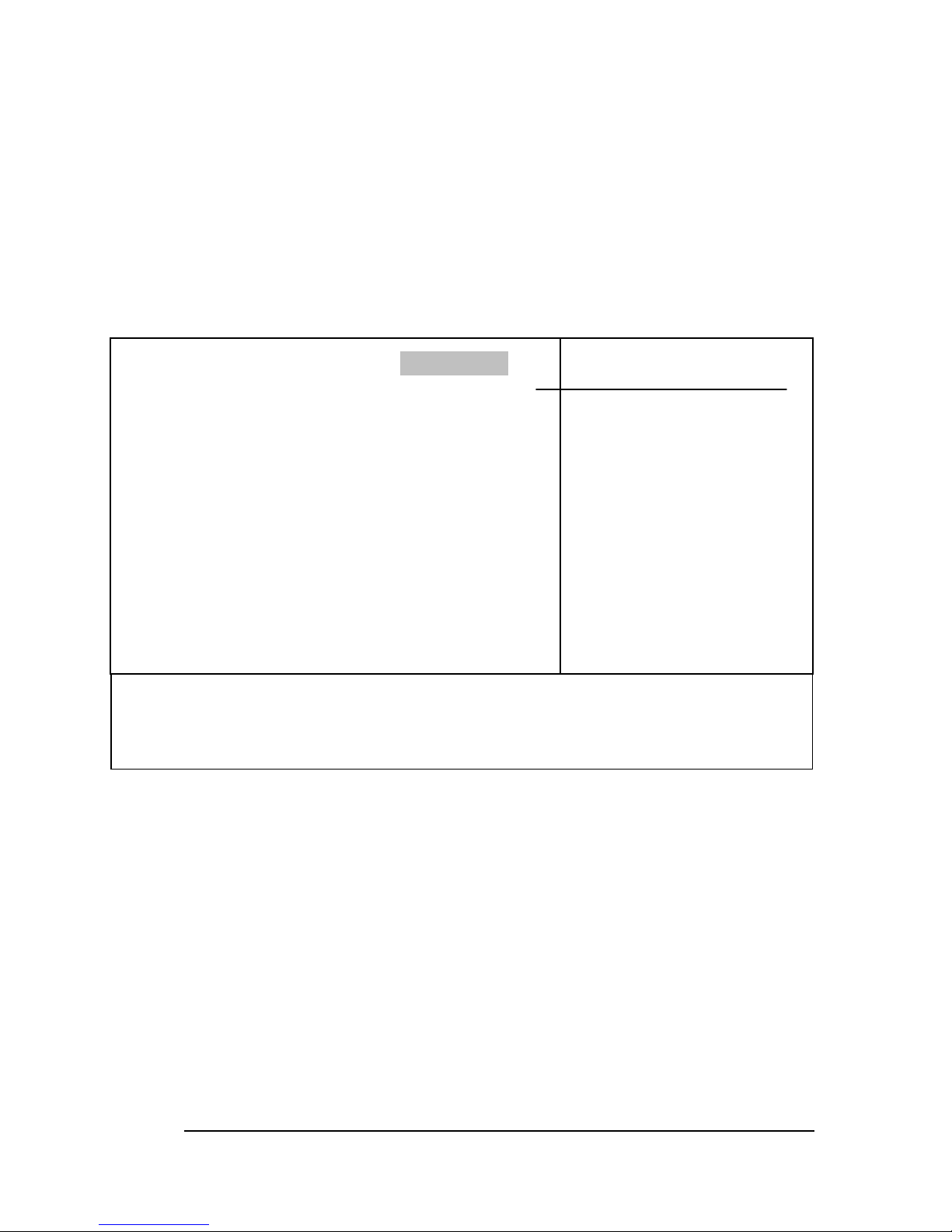
IDE Adapters
The IDE adapters control the hard disk drive. Use a separate sub menu to
configure each hard disk drive.
Figure 2 shows the IDE primary master sub menu.
CMOS Setup Utility – Copyright © 1984-2000 Award Software
IDE Primary Master
IDE HDD Auto-Detection Press Enter
IDE Primary Master Auto
Access Mode Auto
Capacity 10243 MB
Cylinder 19846
Head 16
Precomp 0
Landing Zone 19845
Sector 63
Item Help
Menu Level ØØ
To auto-detect the HDD’s
size, head... on this
channel
↑↓←→Move Enter: Select +/-
/PU/PD: Value F10: Save ESC: Exit
F1: General Help
F5: Previous Values F6: Fail-safe defaults F7:Optimized Defaults
Figure 2 IDE Primary Master sub menu
Page 37

33
Use the legend keys to navigate through this menu and exit to the
main menu. Use Table 3 to configure the hard disk.
Item Options Description
IDE HDD Auto-detection Press Enter Press Enter to auto-detect the
HDD on this channel. If
detection is successful, it fills
the remaining fields on this
menu.
IDE Primary Master None
Auto
Manual
Selecting ‘manual’ lets you set
the remaining fields on this
screen. Selects the type of
fixed disk. "User Type" will let
you select the number of
cylinders, heads, etc. Note:
PRECOMP=65535 means
NONE!
Capacity Auto Display your
disk drive size
Disk drive capacity
(Approximated). Note that this
size is usually slightly greater
than the size of a formatted
disk given by a disk-checking
program.
Access Mode CHS
LBA
Large
Auto
Choose the access mode for
this hard disk
The following options are selectable only if the ‘IDE Primary Master’ item is set to
‘Manual’
Cylinder Min = 0
Max = 65535
Set the number of cylinders for
this hard disk.
Head Min = 0
Max = 255
Set the number of read/write
heads
Precomp Min = 0
Max = 65535
**** Warning: Setting a value of
65535 means no hard disk
Landing zone Min = 0
Max = 65535
****
Sector Min = 0
Max = 255
Number of sectors per track
Table 3 Hard disk selections
Page 38

34
LCD&CRT: This field may appear as an alternative to the video
Field. Select your video display device.
LCD: Liquid Crystal Display
CRT: Auxiliary monitor. When you want to use CRT only, please
select this option. The CRT will have good screen.
Both: Display on both device. When you want to use both display,
please select this option.
Panel: This field have eight option that have
1024x768 DSTN,
640X480 MONO,
640X480 DSTN ,
800X600 DSTN ,
640X480 TFT(12bits),
640X480 TFT(18bits),
1024X768 TFT,
800X600 TFT.
Please refer to page 14 .
Page 39

35
4.6 Advanced BIOS Features
This section allows you to configure your system for basic operation. You
have the opportunity to select the system’s default speed, boot-up
sequence, keyboard operation, shadowing and security.
CMOS Setup Utility – Copyright © 1984 – 2000 Award Software
Advanced BIOS Features
Virus Warning Disabled
Enabled
CPU Internal Cache Enabled
Quick Power On Self Test Enabled
First Boot Device Floppy
Second Boot device HDD-0
Third Boot device LS120
Boot other device Enabled
Swap Floppy Drive Disabled
Boot Up Floppy Seek Enabled
Boot Up NumLock Status On
Typematic Rate Setting Disabled
Typematic Rate (Chars/Sec) 6
Typematic Delay (Msec) 250
Security Option Setup
OS Select For DRAM > 64MB Non-
OS2
Report NO FDD For Win 95 No
Video BIOS Shadow Enabled
C8000-CBFFF Shadow Disabled
CC000-CFFFF Shadow Disabled
Item Help
_______________________
Menu Level Ø
Allow you to choose the
VIRUS warning feature for
IDE Hard Disk boot sector
protection. If this function is
enabled and someone
attempt to write data into
this area, BIOS will show a
warning message on screen
and alarm beep
↑↓←→Move Enter: Select +/-/PU/PD: Value F10: Save ESC: Exit
F1: General Help
F5: Previous Values F6: Fail-safe defaults F7:Optimized Defaults
Page 40
36
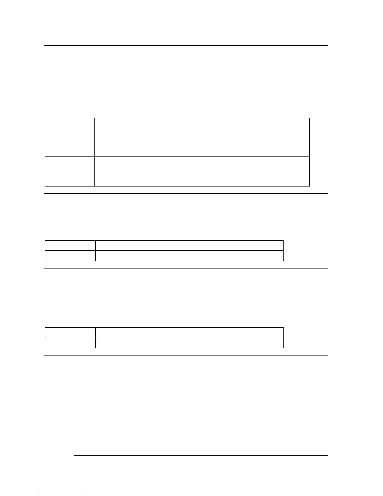
Virus Warning
Allow you to choose the VIRUS Warning feature for IDE Hard Disk boot
sector protection. If this function is enabled and someone attempt to write
data into this area, BIOS will show a warning message on screen and alarm
beep.
Enabled Activates automatically when the system boots up
causing a warning message to appear when anything
attempts to access the boot sector or hard disk partition
table.
Disabled No warning message will appear when anything
attempts to access the boot sector or hard disk partition
table.
CPU Internal Cache/External Cache
These two categories speed up memory access. However, it depends on
CPU/chipset design.
Enabled Enable cache
Disabled Disable cache
Quick Power On Self Test
This category speeds up Power On Self Test (POST) after you power up the
computer. If it is set to Enable, BIOS will shorten or skip some check items
during POST.
Enabled Enable quick POST
Disabled Normal POST
First/Second/Third/Other Boot Device
The BIOS attempts to load the operating system from the devices in the
specified sequence.
The Choice: Floppy, LS120, HDD0-3, SCSI, CDROM, ZIP 100, LAN, and
Disabled.
Page 41

37
Swap Floppy Drive
If the system has two floppy drives, you can swap the logical drive name
assignments.
The choice: Enabled/Disabled.
Boot Up Floppy Seek
Seeks disk drives during boot up. Disabling speeds boot up.
The choice: Enabled/Disabled.
Boot Up NumLock Status
Select power on state for NumLock.
The choice: On/Off.
Typematic Rate Setting
Keystrokes repeat at a rate determined by the keyboard controller. When
enabled, the typematic rate and typematic delay can be selected.
The choice: Enabled/Disabled.
Typematic Rate (Chars/Sec)
Sets the number of times a second to repeat a keystroke when you hold the
key down.
The choice: 6, 8, 10, 12, 15, 20, 24, and 30.
Typematic Delay (Msec)
Sets the delay time after the key is held down before it begins to repeat the
keystroke.
The choice: 250, 500, 750, 1000.
Page 42

38
Security Option
Select whether the password is required every time the system boots or
only when you enter setup.
System The system will not boot and access to Setup will be
denied if the correct password is not entered at the
prompt.
Setup The system will boot, but access to Setup will be denied if
the correct password is not entered at the prompt.
Note: To disable security, select PASSWORD SETTING at Main Menu and
then you will be asked to enter password. Do not type anything and just
press <Enter>, it will disable security. Once the security is disabled, the
system will boot and you can enter Setup freely.
OS Select For DRAM > 64MB
Select the operating system that is running with greater than 64MB of RAM
on the system.
The choice: Non-OS2, OS2.
Report No FDD For Win 95
Whether report no FDD for Win 95 or not.
The choice: Yes, No.
Page 43

39
4.7 Integrated Peripherals
CMOS Setup Utility – Copyright © 1984 – 2000 Award Software
Integrated Peripherals
On-Chip IDE Channel0 Enabled
On-Chip IDE Channel1 Enabled
IDE Prefetch Mode Enabled
IDE Primary Master PIO Auto
IDE Primary Slave PIO Auto
IDE Secondary Master PIO Auto
IDE Secondary Slave PIO Auto
IDE Primary Master UDMA Auto
IDE Primary Slave UDMA Auto
IDE Secondary Master UDMA Auto
IDE Secondary Slave UDMA Auto
On Chip USB Enabled
AC97 Audio Auto
IDE HDD Block Mode Enabled
Onboard FDD Controller Enabled
Onboard Serial Port 1 3F8/IRQ4
Onboard Serial Port 2 2F8/IRQ3
UART 2 Mode Standard
X IR Function Duplex Half
X TX, RX inverting enable No, Yes
Onboard Parallel Port 378/IRQ7
Onboard Parallel Mode Normal
X ECP Mode Use DMA 3
X Parallel Port EPP Type EPP1, 9
Item Help
________________
Menu Level Ø
If your IDE hard
drive supports block
mode select Enabled
for automatic
detection of the
optimal number of
block read/write per
sector the drive can
support
↑↓←→ Move Enter: Select +/-/PU/PD: Value F10: Save ESC: Exit F1:
General Help
F5: Previous Values F6: Fail-safe defaults F7:Optimized Defaults
There is some item in bottom of scroll.
On-Chip Primary/Secondary PCI IDE
The integrated peripheral controller contains an IDE interface with support
for two IDE channels. Select Enabled to activate each channel separately.
The choice: Enabled, Disabled.
Page 44

40
IDE Primary/Secondary Master/Slave PIO
The four IDE PIO (Programmed Input/Output) fields let you set a PIO mode
(0-4) for each of the four IDE devices that the onboard IDE interface
supports. Modes 0 through 4 provide successively increased performance.
In Auto mode, the system automatically determines the best mode for each
device.
The choice: Auto, Mode 0, Mode 1, Mode 2, Mode 3, Mode 4.
IDE Primary/Secondary Master/Slave UDMA
Ultra DMA-33/66 implementation is possible only if your IDE hard drive
supports it and the operating environment includes a DMA driver (Windows
95 OSR2 or a third-party IDE bus master driver). If your hard drive and your
system software both support Ultra DMA-33/66, select Auto to enable BIOS
support.
The Choice: Auto, Disabled.
OnChip USB
Select Enabled if your system contains a Universal Serial Bus (USB)
controller and you have USB peripherals.
The Choice: Enabled, Disabled.
USB Keyboard Support
Select Enabled if your system contains a Universal Serial Bus (USB)
controller and you have a USB keyboard.
The Choice: Enabled, Disabled.
Page 45

41
AC’97 Audio
This item allows you to decide to enable/disable the VT82C686A chipset
family to support AC97 Audio.
The choice: Auto, Disabled.
IDE HDD Block Mode
Block mode is also called block transfer, multiple commands, or multiple
sector read/write. If your IDE hard drive supports block mode (most new
drives do), select Enabled for automatic detection of the optimal number of
block read/writes per sector the drive can support.
The choice: Enabled, Disabled
Onboard FDD Controller
Select Enabled if your system has a floppy disk controller (FDC) installed
on the system board and you wish to use it. If you install and-in FDC or the
system has no floppy drive, select Disabled in this field.
The choice: Enabled, Disabled
Onboard Serial Port 1/Port 2
Select an address and corresponding interrupt for the first and second serial
ports.
The choice: 3F8/IRQ4, 2E8/IRQ3, 3E8/IRQ4, 2F8/IRQ3, Disabled,
Auto
UART Mode Select
Select a serial port 2 operation mode.
The choice: Normal, IrDA, ASKIR
Page 46

42
Onboard Parallel Port
Select an address and corresponding interrupt for the parallel ports.
The choice: 378/IRQ7, 278/IRQ5, 3BC/IRQ7, Disabled,
Parallel Port Mode
Select a parallel operation mode.
The choice: SPP, EPP, ECP,ECP+EPP
Page 47

43
4.8 Power Management Setup
The Power Management Setup allows you to configure you system to most
effectively save energy while operating in a manner consistent with your
own style of computer use.
CMOS Setup Utility – Copyright © 1984 – 2000 Award Software
Power Management Setup
ACPI function Enabled
Power Management User Define
Video Off Method Blank Screen
Standby Mode Disabled
Suspend Mode Disabled
HDD Power Down Disabled
Soft-Off by PWR-BTN Instant-Off
Power On by Ring Disabled
Resume by Alarm Disabled
x Date(of month)Alarm 5
x Time(hh:mm:ss)Alarm 0 0 0
** Reload Global Timer Events **
Primary IDE 0 Disabled
Primary IDE 1 Disabled
Secondary IDE 0 Disabled
Item Help
_______________________
Menu Level Ø
↑↓←→Move Enter: Select +/-/PU/PD: Value F10: Save ESC: Exit F1:
General Help
F5: Previous Values F6: Fail-safe defaults F7:Optimized
Defaults
Page 48

44
ACPI Function
This item allows you to enable/disable the Advanced Configuration and
Power Management (ACPI).
The choice: Enabled, Disabled.
Power Management
This category allows you to select the type (or degree) of power saving and
is directly related to the following modes:
1. HDD Power Down
2. Doze Mode
3. Suspend Mode
There are four selections for Power Management, three of which have fixed
mode settings.
Disable (default) No power management. Disables all four modes
Min. Power Saving Minimum power management. Doze Mode = 1 hr.
Standby Mode = 1 hr., Suspend Mode = 1 hr., and
HDD Power Down = 15 min.
Max. Power Saving
Maximum power management -- ONLY AVAILABLE
FOR SL CPU’s. Doze Mode = 1 min., Standby
Mode = 1 min., Suspend Mode = 1 min., and HDD
Power Down = 1 min.
User Defined Allow you to set each mode individually. When not
disabled, each of the ranges is from 1 min. to 1 hr.
except for HDD Power Down, which ranges from 1
min. to 15 min. and disable.
Page 49

45
Video Off Method
This determines the manner in which the monitor is blanked.
V/H SYNC+Blank This selection will cause the system to turn
off the vertical and horizontal
synchronization ports and write blanks to the
video buffer.
Blank Screen This option only writes blanks to the video
buffer.
DPMS Initial display power management signaling.
Video Off In Suspend
This determines the manner in which the monitor is blanked.
The choice: Yes, No.
Suspend Type
Select the Suspend Type.
The choice: PWRON Suspend, Stop Grant.
MODEM Use IRQ
This determines the IRQ in which the MODEM can use.
The choice: 3, 4, 5, 7, 9, 10, and 11, NA.
Suspend Mode
When enabled and after the set time of system inactivity, all devices except
the CPU will be shut off.
The choice: 1Min, 2Min, 4Min, 8Min, 12Min, 20Min, 30Min, 40Min, 1Hour,
Disabled.
Page 50

46
HDD Power Down
When enabled and after the set time of system inactivity, the hard disk
drive will be powered down while all other devices remain active.
The choice: 1Min, 2Min, 3Min, 4Min, 5Min, 6Min, 7Min, 8Min, 9Min, 10Min,
11Min, 12Min, 13Min, 14Min, 15Min, Disabled.
Soft-Off by PWR-BTN
Pressing the power button for more than 4 seconds forces the system to
enter the Soft-Off state when the system has “hung.”
The choice: Delay 4 Sec, Instant-Off.
Power On by Ring
This item is Disabled or Enabled. This function can power on by ring.
The choice: Enabled, Disabled.
Resume by Alarm
This item is Disabled or Enabled. This function can wake-up system by date
or time.
PM Events
PM events are I/O events whose occurrence can prevent the system from
entering a power saving mode or can awaken the system from such a mode.
In effect, the system remains alert for anything, which occurs to a device,
which is configured as Enabled, even when the system is in a power down
mode.
Primary IDE 0
Primary IDE 1
Secondary IDE 0
Secondary IDE 1
FDD, COM, LPT Port
PCI PIRQ [A-D] #
Page 51
47
4.9 PnP/PCI Configuration Setup
This section describes configuring the PCI bus system. PCI, or Personal
Computer Interconnect, is a system which allows I/O devices to operate at
speeds nearing the speed the CPU itself uses when communicating with its
own special components. This section covers some very technical items
and it is strongly recommended that only experienced users should make
any changes to the default settings.
CMOS Setup Utility – Copyright © 1984-2000 Award Software
PnP/PCI Configurations
PNP OS Installed No
Reset Configuration Data Disabled
Resources Controlled By Auto
(ESCD)
X IRQ Resources Press
Enter
X DMA Resources Press
Enter
PCI/VGA Palette Snoop Disabled
Item Help
------------------------Menu Level Ø
Default is Disabled.
Select Enabled to reset
Extended System
Configuration Data
(ESCD) when you exit
Setup if you have
installed a new add-on
and the system
reconfiguration has
caused such a serious
conflict that the OS
cannot boot
↑↓←→Move Enter: Select +/-/PU/PD: Value F10: Save ESC: Exit
F1: General Help
F5: Previous Values F6: Fail-safe defaults F7:Optimized
Defaults
Page 52

48
Reset Configuration Data
Normally, you leave this field Disabled. Select Enabled to reset Extended
System Configuration Data (ESCD) when you exit Setup if you have
installed a new add-on and the system reconfiguration has caused such a
serious conflict that the operating system cannot boot.
The choice: Enabled, Disabled.
Resource controlled by
The Award Plug and Play BIOS has the capacity to automatically configure
all of the boot and Plug and Play compatible devices. However, this
capability means absolutely nothing unless you are using a Plug and Play
operating system such as Windows95. If you set this field to “manual”
choose specific resources by going into each of the sub menu that follows
this field (a sub menu is preceded by a “Ø”).
The choice: Auto (ESCD), Manual.
IRQ Resources
When resources are controlled manually, assign each system interrupt a
type, depending on the type of device using the interrupt.
IRQ3/4/5/7/9/10/11/12/14/15 assigned to
This item allows you to determine the IRQ assigned to the ISA bus and is
not available to any PCI slot. Legacy ISA for devices compliant with the
original PC AT bus specification, PCI/ISA PnP for devices compliant with
the Plug and Play standard whether designed for PCI or ISA bus
architecture.
The Choice: PCI Device, Reserved.
Page 53

49
PCI/VGA Palette Snoop
Leave this field at Disabled.
Choices are Enabled, Disabled.
4.10 PC Health Status
CMOS Setup Utility – Copyright © 1984-2000 Award Software
PC Health Status
Current System Temp 46¢XC/114
¢XF
Vcore 1.48 V
2.5V 2.47 V
3.3V 3.28 V
5V 5.01 V
Item Help
------------------------Menu Level Ø
↑↓←→ Move Enter: Select +/-/PU/PD: Value F10: Save ESC: Exit F1:
General Help
F5: Previous Values F6: Fail-safe defaults F7:Optimized
Defaults
Page 54

50
4.11 Defaults Menu
Selecting “Defaults” from the main menu shows you two options,
which are described below
Load Fail-Safe Defaults
When you press <Enter> on this item you get a confirmation dialog
box with a message similar to:
Load Fail-Safe Defaults (Y/N)? N
Pressing ‘Y’ loads the BIOS default values for the most stable,
minimal-performance system operations.
Load Optimized Defaults
When you press <Enter> on this item you get a confirmation dialog
box with a message similar to:
Load Optimized Defaults (Y/N)? N
Pressing ‘Y’ loads the default values that are factory settings for
optimal performance system operations.
Page 55

51
4.12 Supervisor/User Password Setting
You can set either supervisor or user password, or both of then. The
differences between are:
Supervisor password:
Can enter and change the options of the setup menus.
User password:
Just can only enter but do not have the right to change the options of the
setup menus. When you select this function, the following message will
appear at the center of the screen to assist you in creating a password.
ENTER PASSWORD:
Type the password, up to eight characters in length, and press <Enter>.
The password typed now will clear any previously entered password from
CMOS memory. You will be asked to confirm the password. Type the
password again and press <Enter>. You may also press <Esc> to abort the
selection and not enter a password.
To disable a password, just press <Enter> when you are prompted to enter
the password. A message will confirm the password will be disabled. Once
the password is disabled, the system will boot and you can enter Setup
freely.
PASSWORD DISABLED.
When a password has been enabled, you will be prompted to enter it every
time you try to enter Setup. This prevents an unauthorized person from
changing any part of your system configuration.
Additionally, when a password is enabled, you can also require the BIOS to
request a password every time your system is rebooted. This would
prevent unauthorized use of your computer.
You determine when the password is required within the BIOS Features
Setup Menu and its Security option (see Section 3). If the Security option is
set to password will be required both at boot and at entry to Setup. If set to
“Setup”, prompting only occurs when trying to enter Setup.
Page 56

52
4.13 Exit Selecting
Save & Exit Setup
Pressing <Enter> on this item asks for confirmation:
Save to CMOS and EXIT (Y/N)? Y
Pressing “Y” stores the selections made in the menus in CMOS – a
special section of memory that stays on after you turn your system
off. The next time you boot your computer, the BIOS configures
your system according to the Setup selections stored in CMOS.
After saving the values the system is restarted again.
Exit Without Saving
Pressing <Enter> on this item asks for confirmation:
Quit without saving (Y/N)? Y
This allows you to exit Setup without storing in CMOS any change.
The previous selections remain in effect. This exits the Setup utility
and restarts your computer.
Page 57

53
Appendix A. Watch-Dog Timer
The Watchdog Timer is a device to ensure that standalone systems can
always recover from abnormal conditions that cause the system to crash.
These conditions may result from an external EMI or a software bug. When
the system stops working, hardware on the board will perform hardware
reset (cold boot) to bring the system back to a known state.
Three I/O ports control the operation of Watchdog Timer.
443 (hex) Write Set Watchdog Time period
443 (hex) Read Enable the refresh the Watchdog Timer.
043/843 (hex) Read Disable the Watchdog Timer.
Prior to enable the Watchdog Timer, user has to set the time-out period.
The resolution of the timer is 1 second and the range of the timer is from 1
sec to 255 sec. You need to send the time-out value to the I/O port – 443H,
and then enable it by reading data from the same I/O port – 443H. This will
activate the timer that will eventually time out and reset the CPU board. To
ensure that this reset condition won’t occur, the Watchdog Timer must be
periodically refreshed by reading the same I/O port 443H. This must be
done within the time-out period that is set by the software, please refer to
the example program. Finally, we have to disable the Watchdog timer by
reading the I/O port -- 843H or 043H. Otherwise the system could reset
unconditionally.
A tolerance of at least 5% must be maintained to avoid unknown routines in the
operating system (DOS), such as disk I/O that can be very time-consuming.
Therefore if the time-out period has been set to 10 seconds, the I/O port 443H
must be read within 7 seconds.
Page 58

54
Example assembly program:
TIMER_PORT = 443H
TIMER_START = 443H
TIMER_STOP = 843H
;;INITIAL TIMER COUNTER
MOV DX, TIMER_PORT
MOV AL, 8 ;;8 seconds
OUT DX, AL
MOV DX, TIMER_START
IN AL, DX. ;;START COUNTER
W_LOOP:
MOV DX, TIMER_STOP
IN AL, DX
MOV DX, TIMER_START
IN AL, DX ;;RESTART COUNTER
;;ADD YOUR APPLICATION HERE
CMP EXIT_AP, 0
JNE W_LOOP
MOV DX, TIMER_STOP
IN AL, DX
;;EXIT AP
Page 59

55
Appendix B. I/O Address Map
B.1 System I/O Address Map
I/O Address Map
Description
000-01F DMA Controller #1
020-021 Interrupt Controller # 1, Master
022-023 Chipset address
040-05F System Timer
060-06F Standard 101/102 keyboard Controller
070-07F Real time Clock, NMI Controller
080-0BF DMA Page Register
0A0-0BF Interrupt Controller # 2
0C0-0DF DMA Controller # 2
0F0-0F0 Clear Math Coprocessor Busy
0F1-0F1 Reset Math Coprocessor
0F8-OFF Math Coprocessor
1F0-1F8 VIR BUS Master PCI IDE Controller
200-207 Game I/O
278-27F Reserved
2F8-2FF Serial Port 2
378-37F Parallel Printer Port 1
3B0-3DF Cyrix Graphic Adapter
3F0-3F7 Floppy Disk Controller
3F8-3FF Serial Port 1
443 Watch dog timer enable
043/843 Watch dog timer disable
Page 60

56
B.2 DMA channel assignments
Channel
Function
0
Available
1
Audio*
2
Floppy disk (8-bit transfer)
3
Parallel**
4
Cascade for DMA controller 1
5
Audio*
6
Available
7
Available
**parallel port DMA default setting: DMA 3
parallel port DMA select: DMA 1.3
Page 61

57
B.3 Interrupt assignments
Interrupt #
Interrupt source
NMI Parity error detected
IRQ 0 System timer
IRQ 1 Keyboard
IRQ 2 Interrupt from controller 2 (cascade)
IRQ 8 Real-time clock
IRQ 9 Available
IRQ 10 Available
IRQ 11 Available
IRQ 12 PS/2 mouse
IRQ 13 Numeric data processor
IRQ 14 Fixed disk controller
IRQ 15 USB controller
IRQ 3 Available
IRQ 4 Serial communication port 1
IRQ 5 Audio*
IRQ 6 Diskette controller (FDC)
IRQ 7 Parallel port 1 (print port)
* Audio default setting: IRQ5
Ethernet IRQ is automatic set by the system
B.4 1st MB memory map
Address Description
F000h-FFFFh System ROM
D800h-EFFFh Unused
D000h-D7FFh Unused
C000h-C9FFh Expansion ROM*
B800h-BFFFh CGA/EGA/VGA text
B000h-B7FFh Unused
A000h-AFFFh EGA/VGA graphics
0000h-9FFFh Base memory
* Default setting
 Loading...