

Page 1

PCIE-9152 PCIMG 1.3 CPU Card
MODEL:
PCIE-9152
PICMG 1.3 CPU Card
Socket 479 for Intel® Pentium® M, Celeron® M CPU
VGA, Dual GbE, SATA and USB 2.0
User Manual
Rev. 1.10 – 17 February, 2009
Page i
Page 2

Date Version Changes
17 February, 2009 1.10 Southbridge changed to Intel® 915GME
Minor edits
23 March, 2007 1.00 Initial release
PCIE-9152 PCIMG 1.3 CPU Card
Revision
Page ii
Page 3

PCIE-9152 PCIMG 1.3 CPU Card
COPYRIGHT NOTICE
The information in this document is subject to change without prior notice in order to
improve reliability, design and function and does not represent a commitment on the part
of the manufacturer.
In no event will the manufacturer be liable for direct, indirect, special, incidental, or
consequential damages arising out of the use or inability to use the product or
documentation, even if advised of the possibility of such damages.
This document contains proprietary information protected by copyright. All rights are
Copyright
reserved. No part of this manual may be reproduced by any mechanical, electronic, or
other means in any form without prior written permission of the manufacturer.
TRADEMARKS
All registered trademarks and product names mentioned herein are used for identification
purposes only and may be trademarks and/or registered trademarks of their respective
owners.
Page iii
Page 4

PCIE-9152 PCIMG 1.3 CPU Card
Packing List
NOTE:
If any of the components listed in the checklist below are missing,
please do not proceed with the installation. Contact the IEI reseller or
vendor you purchased the PCIE-9152 from or contact an IEI sales
representative directly. To contact an IEI sales representative, please
send an email to
The items listed below should all be included in the PCIE-9152 package.
1 x PCIE-9152
1 x IDE cable
1 x SATA power cable
2 x SATA cables
1 x Dual RS-232 cable
1 x Mini jumper pack
1 x Utility CD
1 x QIG (quick installation guide)
Images of the above items are shown in Chapter 3.
sales@iei.com.tw.
Page iv
Page 5

PCIE-9152 PCIMG 1.3 CPU Card
Table of Contents
1 INTRODUCTION.......................................................................................................... 1
1.1 INTRODUCTION........................................................................................................... 2
1.2 BENEFITS ................................................................................................................... 2
1.3 FEATURES................................................................................................................... 2
1.4 OVERVIEW PHOTO...................................................................................................... 3
1.5 PERIPHERAL CONNECTORS AND JUMPERS .................................................................. 3
1.6 TECHNICAL SPECIFICATIONS ...................................................................................... 4
2 DETAILED SPECIFICATIONS.................................................................................. 6
2.1 OVERVIEW.................................................................................................................. 7
2.2 DIMENSIONS............................................................................................................... 7
2.2.1 Board Dimensions.............................................................................................. 7
2.2.2 External Interface Panel Dimensions................................................................ 8
2.3 DATA FLOW................................................................................................................ 9
2.4 CPU........................................................................................................................... 9
2.5 INTEL 915GME NORTHBRIDGE CHIPSET.................................................................. 10
2.5.1 Memory Support................................................................................................11
2.5.2 PCIe x16............................................................................................................11
2.5.3 Analog CRT.......................................................................................................11
2.5.4 LVDS................................................................................................................ 12
2.5.5 SDVO ............................................................................................................... 12
2.5.6 Direct Media Interface (DMI).......................................................................... 12
2.6 INTEL ICH6M SOUTHBRIDGE CHIPSET .................................................................... 12
2.6.1 Audio Codec ’97 Controller............................................................................. 12
2.6.2 IDE Interface ................................................................................................... 13
2.6.3 Low Pin Count (LPC) Interface....................................................................... 13
2.6.4 PCI Interface.................................................................................................... 14
2.6.4.1 PCI GbE Ethernet ..................................................................................... 14
2.6.5 Real Time Clock ............................................................................................... 14
2.6.6 SATA Controller............................................................................................... 14
2.6.7 USB Controller ................................................................................................ 15
Page v
Page 6

2.6.8 PCIe Bus .......................................................................................................... 15
2.7 LPC BUS COMPONENTS ........................................................................................... 15
2.7.1 BIOS Chipset.................................................................................................... 15
2.7.2 Super I/O chipset.............................................................................................. 15
2.7.2.1 LPC Interface............................................................................................ 16
2.7.2.2 16C550 UARTs......................................................................................... 16
2.7.2.3 Enhanced Hardware Monitor.................................................................... 16
2.7.2.4 Fan Speed Controller ................................................................................ 17
2.7.2.5 Parallel Port............................................................................................... 17
2.7.2.6 Keyboard Controller ................................................................................. 17
2.7.3 TPM Connector................................................................................................ 17
2.8 ENVIRONMENTAL AND POWER SPECIFICATIONS ....................................................... 18
2.8.1 System Monitoring........................................................................................... 18
2.8.2 Operating Temperature and Temperature Control........................................... 19
PCIE-9152 PCIMG 1.3 CPU Card
2.8.3 Power Consumption......................................................................................... 19
2.9 EXPANSION OPTIONS................................................................................................ 19
2.9.1 Expansion Options Overview........................................................................... 19
2.9.2 IEI Expansion PICMG 1.3 Backplanes ........................................................... 19
2.9.3 IEI Chassis....................................................................................................... 20
3 UNPACKING............................................................................................................... 22
3.1 ANTI-STATIC PRECAUTIONS...................................................................................... 23
3.2 UNPACKING.............................................................................................................. 23
3.2.1 Unpacking Precautions.................................................................................... 23
3.3 UNPACKING CHECKLIST........................................................................................... 24
3.3.1 Package Contents............................................................................................. 24
3.3.2 Optional Items.................................................................................................. 25
4 CONNECTOR PINOUTS........................................................................................... 27
4.1 PERIPHERAL INTERFACE CONNECTORS..................................................................... 28
4.1.1 PCIE-9152 Layout........................................................................................... 28
4.1.2 Peripheral Interface Connectors ..................................................................... 28
4.1.3 External Interface Panel Connectors............................................................... 29
4.2 INTERNAL PERIPHERAL CONNECTORS...................................................................... 30
4.2.1 Audio Connector .............................................................................................. 30
Page vi
Page 7

PCIE-9152 PCIMG 1.3 CPU Card
4.2.2 Backlight Inverter Connector .......................................................................... 31
4.2.3 Compact Flash Socket...................................................................................... 32
4.2.4 Fan Connector................................................................................................. 33
4.2.5 Floppy Disk Connector.................................................................................... 34
4.2.6 GPIO Connector.............................................................................................. 36
4.2.7 Front Panel Connector.................................................................................... 36
4.2.8 IDE Connector................................................................................................. 38
4.2.9 Infrared Interface Connector........................................................................... 39
4.2.10 Keyboard and Mouse Connector................................................................... 40
4.2.11 LVDS LCD Connector.................................................................................... 41
4.2.12 Parallel Port Connector ................................................................................ 43
4.2.13 SATA Drive Connectors ................................................................................. 44
4.2.14 SDVO Connector............................................................................................ 45
4.2.15 Serial Port Connector (COM1 & COM2) ..................................................... 46
4.2.16 TPM Connector.............................................................................................. 47
4.3 EXTERNAL PERIPHERAL INTERFACE CONNECTOR PANEL ......................................... 48
4.3.1 LAN Connectors............................................................................................... 48
4.3.2 USB Connector ................................................................................................ 49
4.3.3 VGA Connector................................................................................................ 50
5 INSTALLATION ......................................................................................................... 51
5.1 ANTI-STATIC PRECAUTIONS...................................................................................... 52
5.2 INSTALLATION CONSIDERATIONS.............................................................................. 52
5.2.1 Installation Notices.......................................................................................... 53
5.2.2 Installation Checklist....................................................................................... 53
5.3 CPU, CPU COOLING KIT AND DIMM INSTALLATION.............................................. 54
5.3.1 Socket 479 CPU Installation............................................................................ 55
5.3.2 Cooling Kit Installation ................................................................................... 57
5.3.3 DIMM Installation........................................................................................... 59
5.3.4 CF Card Installation........................................................................................ 61
5.4 JUMPER SETTINGS .................................................................................................... 62
5.4.1 CF Card Setup ................................................................................................. 62
5.4.2 Clear CMOS Jumper........................................................................................ 63
5.4.3 FSB Setup Jumper............................................................................................ 65
5.4.4 LVDS Voltage Selection.................................................................................... 66
Page vii
Page 8

5.5 CHASSIS INSTALLATION............................................................................................ 67
5.5.1 Airflow.............................................................................................................. 67
5.5.2 Backplane Installation..................................................................................... 68
5.5.3 CPU Card Installation..................................................................................... 68
5.6 INTERNAL PERIPHERAL DEVICE CONNECTIONS........................................................ 69
5.6.1 Peripheral Device Cables................................................................................ 69
5.6.2 IDE Cable Connection..................................................................................... 69
5.6.3 5.1 Channel Audio Kit Installation.................................................................. 70
5.6.4 7.1 Channel Audio Kit Installation.................................................................. 72
5.6.5 FDD Cable Connection ................................................................................... 73
5.6.6 Parallel Port Cable.......................................................................................... 74
5.6.7 Dual RS-232 Cable Connection....................................................................... 76
5.6.8 SATA Drive Connection ................................................................................... 77
5.6.9 Dual PS/2 Cable .............................................................................................. 79
PCIE-9152 PCIMG 1.3 CPU Card
5.7 EXTERNAL PERIPHERAL INTERFACE CONNECTION ................................................... 80
5.7.1 LAN Connection (Single Connector)............................................................... 81
5.7.2 USB Device Connection (Single Connector)................................................... 82
5.7.3 VGA Monitor Connection ................................................................................ 83
6 BIOS..............................................................................................................................84
6.1 INTRODUCTION......................................................................................................... 85
6.1.1 Starting Setup................................................................................................... 85
6.1.2 Using Setup...................................................................................................... 85
6.1.3 Getting Help..................................................................................................... 86
6.1.4 Unable to Reboot After Configuration Changes.............................................. 86
6.1.5 BIOS Menu Bar................................................................................................ 86
6.2 MAIN........................................................................................................................ 87
6.3 ADVANCED............................................................................................................... 88
6.3.1 CPU Configuration.......................................................................................... 90
6.3.2 IDE Configuration........................................................................................... 91
6.3.2.1 IDE Master, IDE Slave............................................................................. 93
6.3.3 Floppy Configuration....................................................................................... 98
6.3.4 Super IO Configuration ................................................................................... 99
6.3.5 Hardware Health Configuration.................................................................... 102
6.3.6 ACPI Configuration....................................................................................... 103
Page viii
Page 9
PCIE-9152 PCIMG 1.3 CPU Card
6.3.7 Remote Access Configuration........................................................................ 104
6.3.8 T rusted Computing......................................................................................... 108
6.3.9 USB Configuration......................................................................................... 109
6.4 PCI/PNP..................................................................................................................110
6.5 BOOT.......................................................................................................................113
6.5.1 Boot Settings Configuration............................................................................114
6.5.2 Boot Device Priority.......................................................................................116
6.5.3 Hard Disk Drives............................................................................................116
6.5.4 Removable Drives...........................................................................................117
6.5.5 CD/DVD Drives..............................................................................................118
6.6 SECURITY............................................................................................................... 120
6.7 CHIPSET ................................................................................................................. 121
6.7.1 Northbridge Configuration............................................................................ 122
6.7.2 Southbridge Chipset Configuration............................................................... 124
6.8 POWER ................................................................................................................... 126
6.9 EXIT....................................................................................................................... 128
7 SOFTWARE INSTALLATION................................................................................ 130
7.1 AVAILABLE SOFTWARE DRIVERS ............................................................................ 131
7.2 DRIVER CD AUTO-RUN.......................................................................................... 131
7.3 CHIPSET DRIVER INSTALLATION............................................................................. 132
7.4 GRAPHICS DRIVER INSTALLATION.......................................................................... 136
7.5 LAN DRIVER INSTALLATION.................................................................................. 141
7.6 AUDIO DRIVER INSTALLATION ............................................................................... 145
7.6.1 BIOS Setup..................................................................................................... 145
7.6.2 Driver Installation ......................................................................................... 146
A BIOS OPTIONS ........................................................................................................ 150
B TERMINOLOGY...................................................................................................... 154
C DIGITAL I/O INTERFACE..................................................................................... 158
C.1 INTRODUCTION...................................................................................................... 159
C.2 DIO CONNECTOR PINOUTS.................................................................................... 159
C.3 ASSEMBLY LANGUAGE SAMPLES........................................................................... 160
C.3.1 Enable the DIO Input Function..................................................................... 160
C.3.2 Enable the DIO Output Function.................................................................. 160
Page ix
Page 10

D WA TCHDOG TIMER .............................................................................................. 161
E ADDRESS MAPPING .............................................................................................. 164
E.1 DIRECT MEMORY ACCESS (DMA)......................................................................... 165
E.2 INPUT/OUTPUT (IO)............................................................................................... 165
E.3 INTERRUPT REQUEST (IRQ)................................................................................... 167
E.4 MEMORY................................................................................................................ 168
F HAZARDOUS MATERIALS DISCLOSURE........................................................ 169
F.1 HAZARDOUS MATERIALS DISCLOSURE TABLE FOR IPB PRODUCTS CERTIFIED AS
ROHS COMPLIANT UNDER 2002/95/EC WITHOUT MERCURY..................................... 170
PCIE-9152 PCIMG 1.3 CPU Card
Page x
Page 11

PCIE-9152 PCIMG 1.3 CPU Card
List of Figures
Figure 1-1: PCIE-9152 Overview [Front View]..............................................................................3
Figure 2-1: PCIE-9152 Dimensions (mm) .....................................................................................7
Figure 2-2: External Interface Panel Dimensions (mm)..............................................................8
Figure 2-3: Data Flow Block Diagram...........................................................................................9
Figure 2-4: Northbridge................................................................................................................11
Figure 2-5: Southbridge...............................................................................................................12
Figure 2-6: Super I/O Chipset......................................................................................................16
Figure 4-1: Connector and Jumper Locations...........................................................................28
Figure 4-2: Audio Connector Pinouts (10-pin)...........................................................................30
Figure 4-3: Panel Backlight Connector Pinout Locations........................................................31
Figure 4-4: CF Card Socket Location .........................................................................................32
Figure 4-5: +12 V Fan Connector Location................................................................................34
Figure 4-6: 34-pin FDD Connector Location..............................................................................35
Figure 4-7: GPIO Connector Pinout Locations..........................................................................36
Figure 4-8: Front Panel Connector Pinout Locations...............................................................37
Figure 4-9: Secondary IDE Device Connector Locations.........................................................38
Figure 4-10: Infrared Connector Pinout Locations ...................................................................40
Figure 4-11: Keyboard and Mouse Connector Location...........................................................41
Figure 4-12: LVDS LCD Connector Pinout Locations...............................................................42
Figure 4-13: Parallel Port Connector Location..........................................................................43
Figure 4-14: SATA Drive Connector Locations.........................................................................44
Figure 4-15: SDVO Connector Pinout Locations.......................................................................45
Figure 4-16: COM1 and COM2 Connector Pinout Locations ...................................................46
Figure 4-17: TPM Connector Pinout Locations .........................................................................47
Figure 4-18: PCIE-9152 External Peripheral Interface Connector ...........................................48
Figure 4-19: RJ-45 Ethernet Connector......................................................................................49
Figure 4-20: VGA Connector .......................................................................................................50
Figure 5-1: Make sure the CPU socket retention screw is unlocked ......................................56
Figure 5-2: Lock the CPU Socket Retention Screw...................................................................57
Figure 5-3: Cooling Kit.................................................................................................................57
Page xi
Page 12

Figure 5-4: Cooling Kit Support Bracket....................................................................................58
Figure 5-5: Connect the cooling fan cable.................................................................................59
Figure 5-6: Installing a DIMM.......................................................................................................60
Figure 5-7: CF Card Installation..................................................................................................61
Figure 5-8: CF Card Setup Jumper Location.............................................................................63
Figure 5-9: Clear CMOS Jumper .................................................................................................65
Figure 5-10: FSB Setup Jumper Jumper....................................................................................66
Figure 5-11: LVDS Voltage Selection Jumper Pinout Locations.............................................67
Figure 5-12: IDE Cable Connection.............................................................................................70
Figure 5-13: 5.1 Channel Audio Kit.............................................................................................71
Figure 5-14: 5.1 Channel Audio Kit.............................................................................................73
Figure 5-15: FDD Cable Connection...........................................................................................74
Figure 5-16: LPT Cable Connection............................................................................................75
Figure 5-17: Connect the LPT Device.........................................................................................76
PCIE-9152 PCIMG 1.3 CPU Card
Figure 5-18: Dual RS-232 Cable Installation..............................................................................77
Figure 5-19: SATA Drive Cable Connection...............................................................................78
Figure 5-20: SATA Power Drive Connection..............................................................................79
Figure 5-21: Keyboard/Mouse Cable Connection .....................................................................80
Figure 5-22: LAN Connection......................................................................................................81
Figure 5-23: USB Device Connection.........................................................................................82
Figure 5-24: VGA Connector .......................................................................................................83
Figure 7-1: Introduction Screen............................................................................................... 132
Figure 7-2: Available Drivers.................................................................................................... 132
Figure 7-3: Chipset Driver Installation Program..................................................................... 133
Figure 7-4: Chipset Driver Installation Welcome Screen....................................................... 133
Figure 7-5: Chipset Driver Installation License Agreement.................................................. 134
Figure 7-6: Chipset Driver Readme File Information ............................................................. 134
Figure 7-7: Chipset Driver Readme File Information ............................................................. 135
Figure 7-8: Chipset Driver Installation Complete................................................................... 135
Figure 7-9: Select the Operating System ................................................................................ 136
Figure 7-10: VGA Driver............................................................................................................ 137
Figure 7-11: GMA Driver Readme File..................................................................................... 138
Figure 7-12: GMA Driver File Extraction ................................................................................. 138
Figure 7-13: GMA Driver Installation Welcome Screen ......................................................... 139
Figure 7-14: GMA Driver License Agreement......................................................................... 140
Page xii
Page 13

PCIE-9152 PCIMG 1.3 CPU Card
Figure 7-15: GMA Driver Installing Notice .............................................................................. 140
Figure 7-16: GMA Driver Installation Complete...................................................................... 141
Figure 7-17: LAN Driver Setup File.......................................................................................... 142
Figure 7-18: RTL8110SC InstallShield Wizard........................................................................ 142
Figure 7-19: LAN Driver InstallShield Wizard Continues....................................................... 143
Figure 7-20: LAN Driver InstallShield Wizard Welcome Screen........................................... 143
Figure 7-21: LAN Driver Ready Screen ................................................................................... 144
Figure 7-22: LAN Drivers Installing.......................................................................................... 144
Figure 7-23: LAN Driver InstallShield Wizard ......................................................................... 145
Figure 7-24: LAN Driver Installation Complete....................................................................... 145
Figure 7-25: 4-AUDIO\AC-KIT883HD\Windows Folder........................................................... 146
Figure 7-26: HD Audio Driver Setup Extracting Files ............................................................ 147
Figure 7-27: HD Audio Driver Setup Welcome Screen .......................................................... 148
Figure 7-28: HD Audio Driver Installation Complete.............................................................. 149
Page xiii
Page 14

PCIE-9152 PCIMG 1.3 CPU Card
List of Tables
Table 1-1: Technical Specifications..............................................................................................5
Table 2-1: Supported Processors...............................................................................................10
Table 2-2: Supported HDD Specifications..................................................................................13
Table 2-3: Power Consumption...................................................................................................19
Table 2-4: Compatible IEI PICMG 1.3 Backplanes.....................................................................20
Table 2-5: Compatible IEI Chassis..............................................................................................21
Table 3-1: Package List Contents...............................................................................................25
Table 3-2: Optional Items.............................................................................................................26
Table 4-1: Peripheral Interface Connectors...............................................................................29
Table 4-2: Rear Panel Connectors..............................................................................................30
Table 4-3: Audio Connector Pinouts (10-pin)............................................................................31
Table 4-4: Panel Backlight Connector Pinouts..........................................................................32
Table 4-5: CF Card Socket Pinouts.............................................................................................33
Table 4-6: +12 V Fan Connector Pinouts....................................................................................34
Table 4-7: 34-pin FDD Connector Pinouts .................................................................................35
Table 4-8: GPIO Connector Pinouts............................................................................................36
Table 4-9: Front Panel Connector Pinouts.................................................................................37
Table 4-10: Secondary IDE Connector Pinouts.........................................................................39
Table 4-11: Infrared Connector Pinouts.....................................................................................40
Table 4-12: Keyboard and Mouse Connector Pinouts..............................................................41
Table 4-13: LVDS LCD Port Connector Pinouts........................................................................42
Table 4-14: Parallel Port Connector Pinouts .............................................................................44
Table 4-15: SATA Drive Connector Pinouts...............................................................................45
Table 4-16: SDVO Pinouts ...........................................................................................................46
Table 4-17: COM1 and COM2.......................................................................................................47
Table 4-18: TPM Connector Pinouts...........................................................................................48
Table 4-19: LAN Pinouts ..............................................................................................................49
Table 4-20: RJ-45 Ethernet Connector LEDs.............................................................................49
Table 4-21: USB Port Pinouts......................................................................................................50
Table 4-22: VGA Connector Pinouts...........................................................................................50
Page xiv
Page 15

PCIE-9152 PCIMG 1.3 CPU Card
Table 5-1: Jumpers.......................................................................................................................62
Table 5-2: CF Card Setup Jumper Settings ...............................................................................63
Table 5-3: Clear CMOS Jumper Settings....................................................................................64
Table 5-4: FSB Setup Jumper Settings ......................................................................................65
Table 5-5: LVDS Voltage Selection Jumper Settings................................................................67
Table 5-6: IEI Provided Cables....................................................................................................69
Table 6-1: BIOS Navigation Keys................................................................................................86
Page xv
Page 16

PCIE-9152 PCIMG 1.3 CPU Card
BIOS Menus
BIOS Menu 1: Main.......................................................................................................................87
BIOS Menu 2: Advanced.............................................................................................................. 89
BIOS Menu 3: CPU Configuration...............................................................................................90
BIOS Menu 4: IDE Configuration.................................................................................................91
BIOS Menu 5: IDE Master and IDE Slave Configuration...........................................................93
BIOS Menu 6: Floppy Configuration...........................................................................................98
BIOS Menu 7: Super IO Configuration........................................................................................99
BIOS Menu 8: Hardware Health Configuration....................................................................... 102
BIOS Menu 9: ACPI Configuration........................................................................................... 103
BIOS Menu 10: Remote Access Configuration [Advanced].................................................. 104
BIOS Menu 11: Trusted Computing......................................................................................... 108
BIOS Menu 12: USB Configuration.......................................................................................... 109
BIOS Menu 13: PCI/PnP Configuration.................................................................................... 111
BIOS Menu 14: Boot.................................................................................................................. 113
BIOS Menu 15: Boot Settings Configuration.......................................................................... 114
BIOS Menu 16: Boot Device Priority Settings ........................................................................ 116
BIOS Menu 17: Hard Disk Drives ............................................................................................. 117
BIOS Menu 18: Removable Drives........................................................................................... 118
BIOS Menu 19: CD/DVD Drives ................................................................................................ 119
BIOS Menu 20: Security............................................................................................................ 120
BIOS Menu 21: Chipset............................................................................................................. 121
BIOS Menu 22:Northbridge Chipset Configuration................................................................ 122
BIOS Menu 23: Southbridge Chipset Configuration.............................................................. 124
BIOS Menu 24:Power................................................................................................................. 126
BIOS Menu 25:Exit..................................................................................................................... 128
Page xvi
Page 17

PCIE-9152 PCIMG 1.3 CPU Card
Chapter
1
1 Introduction
Page 1
Page 18

1.1 Introduction
The PCIE-9152 PICMG 1.3 CPU card is a Socket 479 Intel® Pentium® M or Intel®
Celeron® M CPU platform. The PCIE-9152 has a maximum front side bus (FSB)
frequency of 533 MHz and supports two 533 MHz 1 GB dual channel DDR2 memory
modules. The PCIE-9152 also comes with dual PCI Gigabit Ethernet and has flexible
storage options including support for two serial ATA (SATA) hard disk drives (HDD), two
IDE HDD, a CompactFlash® Type II (CF Type II) disk, and a floppy disk drive (FDD).
Optional v1.2 Trusted Platform Modules (TPM) are available as plug-in devices to further
ensure system security.
A PCIE-9152 CPU card with a preinstalled 600 MHz Intel® Celeron® M CPU with a 512K
L2 cache is also available.
1.2 Benefits
PCIE-9152 PCIMG 1.3 CPU Card
Some of the PCIE-9152 benefits are listed below:
Multiple display output options
Storage flexibility with support for SATA drives, IDE drives and CF Type II
DDR2 support enables faster data transfers
Multiple I/O interfaces provide connectivity to a broad range of external
Optional TPMs for secure system bootup
1.3 Features
Some of the PCIE-9152 features are listed below.
Support for the following Socket 479 processors:
Maximum FSB of 533 MHz
disks
peripheral devices
o Intel® Pentium® M
o Intel® Celeron® M
Page 2
Maximum of 2 GB dual-channel memory supported with two 240-pin dual
channel 400 MHz or 533 MHz 1 GB DDR2 DIMMs
Two SATA drives with transfer rates of 1.5 Gb/s supported
Page 19
PCIE-9152 PCIMG 1.3 CPU Card
High performance PCIe GbE Ethernet controllers
Six USB 2.0 devices supported
Multiple display options including CRT, 24-bit dual-channel LVDS
PICMG 1.3 form factor
RoHS compliant
1.4 Overview Photo
The PCIE-9152 has a wide variety of internal and external peripheral connectors. A
labeled photo of the peripheral connectors on the front of the PCIE-9152 is shown in
Figure 1-1.
Figure 1-1: PCIE-9152 Overview [Front View]
1.5 Peripheral Connectors and Jumpers
The PCIE-9152 has the following connectors on-board:
1 x Audio connector
1 x Compact flash connector
2 x Fan connectors
1 x Floppy disk drive (FDD) connector
1 x Front panel connector
1 x 8-bit general purpose Input/output (GPIO) connector
Page 3
Page 20

1 x IDE disk drive connector
1 x Infrared interface connector
1 x Inverter connector
1 x Keyboard and mouse connector
1 x LVDS connector
2 x Serial port connectors (internal COM 1 and COM 2 RS-232)
2 x Serial ATA (SATA) drive connectors
1 x Serial digital video out (SDVO) connector
1 x TPM connector
The PCIE-9152 has the following external peripheral interface connectors on the board
rear panel
2 x Ethernet connectors
2 x USB port connectors
PCIE-9152 PCIMG 1.3 CPU Card
1 x VGA connector
The PCIE-9152 has the following on-board jumpers:
Clear CMOS
FSB select
LCD voltage selector
CF card setting
1.6 Technical Specifications
PCIE-9152 technical specifications are listed in Table 1-1. See Chapter 2 for details.
Specification PCIE-9152
Form Factor
System CPU
PICMG 1.3
Socket 479 Intel® Pentium® M
Socket 479 Intel® Celeron® M
Page 4
Front Side Bus
System Chipset
400 MHz or 533 MHz
Northbridge: Intel 915GME
Southbridge: Intel ICH6M
Page 21

PCIE-9152 PCIMG 1.3 CPU Card
Specification PCIE-9152
Memory
Display
BIOS
Audio
LAN
COM
USB2.0
IDE
Floppy Disk Drive
SATA
Two 240-pin DIMM sockets support two dual-channel
400 MHz or 533 MHz DDR2 DIMMs with a maximum
capacity of 1 GB each
CRT: Integrated in the Intel 915GME to support CRT
LVDS: Dual channel 24-bit LVDS LCD panel
AMI Flash BIOS
7.1 channel or 5.1 channel audio with an optional AC-KIT
Dual PCI GbE Realtek RTL8110SC chipsets
Two RS-232 seri al ports
Six USB 2.0 devices supported
One 40-pin IDE connects to two Ultra ATA33/66/100
devices
One FDD connector connects to a single FDD
Two 1.5 Gb/s SATA drives supported
Keyboard/mouse
Super I/O
Digital I/O
Infrared
SSD
Watchdog Timer
Power Supply
Temperature
Humidity (operating)
Dimensions (LxW)
Weight (GW/NW)
Table 1-1: Technical Specifications
6-pin box header
ITE IT8712F
One 8-bit digital I/O connector (4-bit input / 4-bit output)
One Infrared connector
CF Type II
Software programmable 1-255 sec. by super I/O
ATX supported
0ºC – 60ºC (32ºF - 140ºF)
5%~95% non-condensing
338.58 mm x 126.39 mm
1100g/ 380g
Page 5
Page 22

PCIE-9152 PCIMG 1.3 CPU Card
Chapter
2
2 Detailed Specifications
Page 6
Page 23
PCIE-9152 PCIMG 1.3 CPU Card
2.1 Overview
This chapter describes the specifications and on-board features of the PCIE-9152 in
detail.
2.2 Dimensions
2.2.1 Board Dimensions
The dimensions of the board are listed below:
Length: 338.58 mm
Width: 126.39 mm
Figure 2-1: PCIE-9152 Dimensions (mm)
Page 7
Page 24
2.2.2 External Interface Panel Dimensions
External peripheral interface connector panel dimensions are shown in Figure 2-2.
Figure 2-2: External Interface Panel Dimensions (mm)
PCIE-9152 PCIMG 1.3 CPU Card
Page 8
Page 25
PCIE-9152 PCIMG 1.3 CPU Card
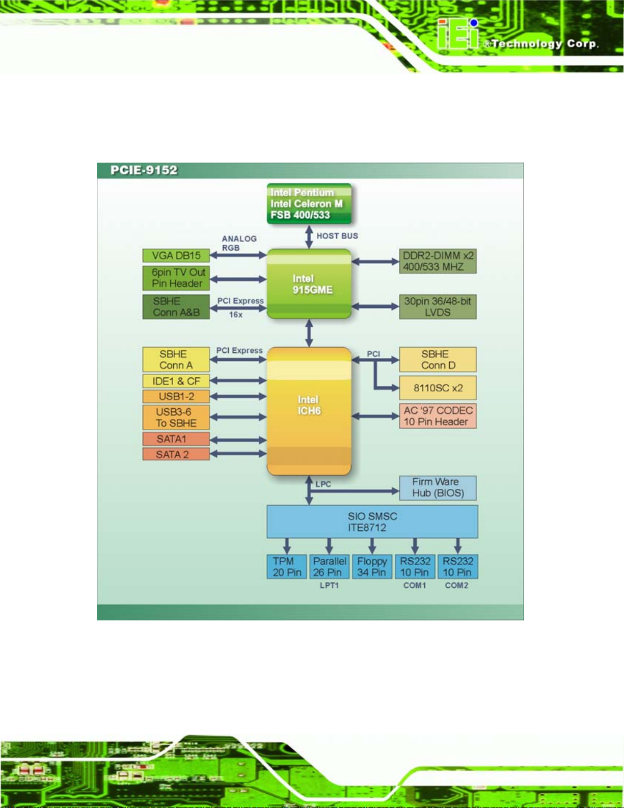
2.3 Data Flow
Figure 2-3 shows the data flow between the two on-board chipsets and other components
installed on the motherboard and described in the following sections of this chapter.
Figure 2-3: Data Flow Block Diagram
2.4 CPU
The PCIE-9152 supports the following socket 479 processors:
Page 9
Page 26

PCIE-9152 PCIMG 1.3 CPU Card
Intel® Pentium® M processors
Intel® Celeron® M processors
All the above processors communicate with the Intel 915GME Northbridge chipset through
a 533 MHz or 400 MHz front side bus (FSB). Compatible processors are listed in
Table 2-1.
Family CPU
Speed
Pentium® M
Celeron® M
2.13 GHz 770 533 MHz 90 nm C0 2 MB
2.10 GHz N/A 400 MHz 90 nm B1 2 MB
2 GHz 760 533 MHz 90 nm C0 2 MB
1.86 GHz 750 533 MHz 90 nm C0 2 MB
1.73 GHz 740 533 MHz 90 nm C0 2 MB
1.60 GHz 778 400 MHz 90 nm C0 2 MB
1.60 GHz 730 533 MHz 90 nm C0 2 MB
1.40 GHz N/A 400 MHz 90 nm B0 2 MB
1.10 GHz N/A 400 MHz 90 nm B1 2 MB
1.40 GHz 360 400 MHz 90 nm B1 1 MB
1.30 GHz 350 400 MHz 90 nm B1 1 MB
1.30 GHz 320 400 MHz 130 nm B1 512 KB
Processor #
Bus
Speed
Mfg Tech Stepping
Cache
Size
1.30 GHz 350 400 MHz 90 nm B1 1 MB
1.20 GHz 310 400 MHz 130 nm B1 512 KB
1 GHz N/A 400 MHz 90 nm C0 1 MB
900 MHz 353 400 MHz 90 nm B1 512 KB
Table 2-1: Supported Processors
2.5 Intel 915GME Northbridge Chipset
The Northbridge connects to the CPU through the FSB and the Southbridge through the
DMI. The Northbridge also connects to the system memory and graphics interfaces.
Page 10
Page 27

PCIE-9152 PCIMG 1.3 CPU Card
Figure 2-4: Northbridge
The integrated graphics and memory controller hub (GMCH) facilitates the flow of
information primarily between the following four interfaces:
Front Side Bus (FSB)
System Memory Interface
Graphics Interface
Direct Media Interface (DMI)
2.5.1 Memory Support
The PCIE-9152 supports two 400/533 MHz DDR2 240-pin DIMMs of up to 1.0 GB each.
The memory socket is shown in
Figure 2-4.
2.5.2 PCIe x16
The PCIe x16 bus interfaces to the backplane through the edge connector. The PCIe x16
interface supports a single PCIe x16 graphics card, or multiple cards PCIe x8, PCIe x4 or
PCIe x1 cards.
2.5.3 Analog CRT
A DB-15 VGA connector on the external peripheral interface connector panel is interfaced
to the Intel 915GME graphics engine. The Analog CRT port supports traditional VGA
monitors with a resolution up to 2048 x 1536.
Page 11
Page 28

2.5.4 LVDS
A 30-pin LVDS crimp connector is interfaced to the Intel 915GME graphics engine. The
LVDS port support dual-channel 24-bit graphics output.
2.5.5 SDVO
The SDVO port connects to an SDVO graphics device. Several SDVO converters are
available, including a SDVO-to-VGA, SDVO-to-DVI and SDVO-to-LVDS.
2.5.6 Direct Media Interface (DMI)
The DMI is a data transport connection between the Northbridge and Southbrid ge.
2.6 Intel ICH6M Southbridge Chipset
The Southbridge connects to most of the I/O interfaces on the motherboard. The
PCIE-9152 PCIMG 1.3 CPU Card
connections are shown below.
Figure 2-5: Southbridge
2.6.1 Audio Codec ’97 Controller
The Audio Codec ’97 (AC’97) controller integrated into the Intel ICH6M complies with
Page 12
AC’97 Component Specification, Version 2.3. The AC’97 controller is connected to the
onboard audio connector. The audio connector is connected to an optional 5.1 channel or
7.1 channel audio kit with an embedded AC’97 audio codec. The AC’97 controller
Page 29

PCIE-9152 PCIMG 1.3 CPU Card
supports up to six PCM audio output channels. Complete surround sound requires
six-channel audio consisting of:
Front left
Front right
Back left
Back right
Center
Subwoofer
2.6.2 IDE Interface
The integrated IDE interface on the Intel ICH6M Southbridge supports two IDE hard disks
and ATAPI devices. PIO IDE transfers up to 16 MB/s and Ultra ATA transfers of 100 MB/s.
The integrated IDE interface is able to support the following IDE HDDs:
Ultra A T A/1 00, with data transfer rates up to 100 MB/s
Ultra A T A/6 6, with data transfer rates up to 66 MB/s
Ultra A T A/3 3, with data transfer rates up to 33 MB/s
Specification Ultra ATA/100 Ultra ATA/66 Ultra ATA/33
IDE devices
PIO Mode
PIO Max Transfer Rate
DMA/UDMA designation
DMA/UDMA Max Transfer
Controller Interface
Table 2-2: Supported HDD Specifications
2 2 2
0 – 4 0 – 4 0 – 4
16.6 MB/s 16.6 MB/s 16.6 MB/s
UDMA 3 - 4 UDMA 3 – 4 UDMA 2
100 MB/s 66 MB/s 33 MB/s
5 V 5 V 5 V
2.6.3 Low Pin Count (LPC) Interface
The Intel ICH6M LPC interface complies with the LPC 1.1 specifications. The LPC bus
from the Intel ICH6M is connected to the following components:
BIOS chipset
Super I/O chipset
Page 13
Page 30

2.6.4 PCI Interface
The PCI interface on the Intel ICH6M is compliant with the PCI Revision 2.3
implementation. Some of the features of the PCI interface are listed below.
PCI Revision 2.3 compliant
33 MHz
5 V tolerant PCI signals (except PME#)
Integrated PCI arbiter supports up to seven PCI bus masters
The PCI bus is connected to an interface gold finger on the bottom of the CPU card and
supports four expansion PCI cards on the backplane.
2.6.4.1 PCI GbE Ethernet
Two PCI lanes are connected to two Realtek RTL8110SC GbE controllers.
PCIE-9152 PCIMG 1.3 CPU Card
The Realtek RTL8110SC PCI GbE controllers combine a triple-speed IEEE 802.3
compliant Media Access Controller (MAC) with a triple-speed Ethernet transceiver, 32-bit
PCI bus controller, and embedded memory. With state-of-the-art DSP technology and
mixed-mode signal technology, they offer high-speed transmission over CAT 5 UTP cable
or CAT 3 UTP (10 Mb/s only) cable. Functions such as Crossover Detection &
Auto-Correction, polarity correction, adaptive equalization, cross-talk cancellation, echo
cancellation, timing recovery, and error correction are implemented to provide robust
transmission and reception capability at high speeds.
2.6.5 Real Time Clock
256 bytes of battery backed RAM is provided by the Motorola MC146818 A real time clock
(RTC) integrated into the Intel ICH6M. The RTC operates on a 3 V battery and
32.768 KHz crystal. The RTC keeps track of the time and stores system data even when
the system is turned off.
2.6.6 SATA Controller
Page 14
The integrated SATA controller on the Intel ICH6M southbridge supports two SATA drives
on the PCIE-9152 with independent DMA operations. SATA controller specifications are
listed below.
Page 31

PCIE-9152 PCIMG 1.3 CPU Card
Supports two SATA drives
Supports 1.5 Gb/s data transfer speeds
Supports Serial ATA Specification, Revision 1.0a
2.6.7 USB Controller
Up to six USB ports are supported on the PCIE-9152. Some USB ports are on the rear I/O
interface, the rest are implemented through the edge connector to the backplane.
2.6.8 PCIe Bus
The Southbridge supports four PCIe x1 channels. The PCIe x1 channels are interfaced to
the backplane through the edge connector.
2.7 LPC Bus Components
The LPC bus is connected to components listed below:
BIOS chipset
Super I/O chipset
TPM connector
2.7.1 BIOS Chipset
The BIOS chipset has a licensed copy of AMI BIOS installed on the chipset. Some of the
BIOS features are listed below:
AMI Flash BIOS
SMIBIOS (DMI) compliant
Console redirection function support
PXE (Pre-boot Execution Environment) support
USB booting support
2.7.2 Super I/O chipset
The iTE IT8712F Super I/O chipset is connected to the Intel ICH6M southbridge through
the LPC bus. The iTE IT8712F is an LPC interface-based Super I/O device that comes
with Environment Controller integration.
Page 15
Page 32

Figure 2-6: Super I/O Chipset
2.7.2.1 LPC Interface
PCIE-9152 PCIMG 1.3 CPU Card
The LPC interface on the Super I/O complies with the Intel® Low Pin Count Specification
Rev. 1.0. The LPC interface supports both LDRQ# and SERIRQ protocols as well as PCI
PME# interfaces.
2.7.2.2 16C550 UARTs
The onboard Super I/O has two integrated 16C550 UARTs that can support the following:
Two standard serial ports (COM1 and COM2)
IrDa 1.0 and ASKIR protocols
Another two chipsets connected to the LPC bus provided connectivity to another two serial
port connectors (COM3 and COM4).
2.7.2.3 Enhanced Hardware Monitor
The Super I/O Enhanced Hardware Monitor monitors three thermal inputs, VBAT
internally, and eight voltage monitor inputs. These hardware parameters are reported in
the BIOS and can be read from the BIOS Hardware Health Configuration menu.
Page 16
Page 33

PCIE-9152 PCIMG 1.3 CPU Card
2.7.2.4 Fan Speed Controller
The Super I/O fan speed controller enables the system to monitor the speed of the fan.
One of the pins on the fan connector is reserved for fan speed detection and interfaced to
the fan speed controller on the Super I/O. The fan speed is then reported in the BIOS.
2.7.2.5 Parallel Port
The Super I/O parallel port (LPT) supports standard mode, enhanced mode and
high-speed mode parallel port devices. The LPT is compliant with the following LPT
modes.
Standard mode
o Bi-directional SPP compliant
Enhanced mode
o EPP v1.7 compliant
o EPP v1.9 compliant
High-speed mode
o ECP, IEEE 1284 compliant
2.7.2.6 Keyboard Controller
The Super I/O keyboard controller can execute the 8042 instruction set. Some of the
keyboard controller features are listed below:
The 8042 instruction is compatible with a PS/2 keyboard and PS/2 mouse
Gate A20 and Keyboard reset output
Supports multiple keyboard power on events
Supports mouse double-click and/or mouse move power on events
2.7.3 TPM Connector
The LPC bus is routed to a 20-pin TPM connector. The TPM connector facilitates the
installation of a TPM. Three IEI TPM are compatible with this connector and are listed
below.
TPM-WI01-R10: 20-pin Winbond TPM
TPM-IN01-R10: 20-pin Infineon TPM
Page 17
Page 34

For more details about the above listed IEI TPM, please contact the IEI reseller or vendor
PCIE-9152 PCIMG 1.3 CPU Card
the PCIE-9152 was purchased from or an IEI sales representative at
2.8 Environmental and Power Specifications
2.8.1 System Monitoring
Three thermal inputs on the PCIE-9152 Super I/O Enhanced Hardware Monitor monitor
the following temperatures:
System temperature
Power temperature
CPU temperature
Eight voltage inputs on the PCIE-9152 Super I/O Enhanced Hardware Monitor monitor the
following voltages:
Vcore
+2.5 V
+3.3 V
sales@iei.com.tw.
+5.0 V
+12.0 V
DDR Vtt
+1.5 V
5 VSB
The PCIE-9152 Super I/O Enhanced Hardware Monitor also monitors the following
voltages internally:
VBAT
The PCIE-9152 Super I/O Enhanced Hardware Monitor also monitors the following fan
speeds:
CPU Fan speed
The values for the above environmental parameters are all recorded in the BIOS
Hardware Health Configuration menu.
Page 18
Page 35

PCIE-9152 PCIMG 1.3 CPU Card
2.8.2 Operating Temperature and Temperature Control
The maximum and minimum operating temperatures for the PCIE-9152 are listed below.
Minimum Operating Temperature: 0ºC (32°F)
Maximum Operating Temperature: 60°C (140°F)
A cooling fan and heat sink must be installed on the CPU. Thermal paste must be
smeared on the lower side of the heat sink before it is mounted on the CPU. Heat sinks
are also mounted on the northbridge and southbridge chipsets to ensure the operating
temperature of these chips remain low.
2.8.3 Power Consumption
Table 2-3 shows the power consumption parameters for the PCIE-9152 running with a
1.2 GHz Intel® Pentium® M processor and with a 512 MB PC4300 CL4 DDR2 DIMM.
Voltage Current
+3.3 V 3.64A
+5 V 1.89A
+12 V 1.75A
Table 2-3: Power Consumption
2.9 Expansion Options
2.9.1 Expansion Options Overview
A number of compatible IEI Technology Corp. PICMG 1.3 backplanes and chassis can be
used to develop and expanded system. These backplanes and chassi s are listed below.
2.9.2 IEI Expansion PICMG 1.3 Backplanes
The backplanes listed in Table 2-4 are compatible with the PCIE-9152 and can be used to
develop highly integrated industrial applications. All of the backplanes listed below have
24-pin ATX connector and a 4-pin ATX connector. For more information about these
backplanes please consult the IEI catalog or contact your vendor, reseller or the IEI sales
team at
sales@iei.com.tw.
Page 19
Page 36
PCIE-9152 PCIMG 1.3 CPU Card
Model Total
Slots
System
Expansion Slots
PCIe
PCI
System
Type
x16 x4 x1
PE-4S 4 One 1 1 - 1 Single
PE-4S2 4 One 1 - - 2 Single
PE-4S3 4 One 1 - 2 - Single
PE-5S 5 One 1 1 - 2 Single
PE-5S2 5 One 1 - 3 - Single
PE-6S-R20 6 One 1 - - 3 Single
PE-6S2 6 One 1 1 - 3 Single
PE-6S3 6 One 1 - 3 1 Single
PE-6SD 5 One 1 - 3 - Single
PE-6SD2 5 One 1 - 2 1 Single
PE-7S 7 One 1 - 2 3 Single
PE-7S2 7 One 1 - 4 1 Single
PE-8S 8 One 1 - 3 3 Single
PE-9S 9 One 1 - 4 3 Single
PE-10S-R20 10 One 1 - 4 4 Single
PE-10S2 10 One 1 - 4 4 Single
One 1 1 - 2 PE-13SD 13
Two 1 - 4 2
PXE-13S 13 One 1 - 3 8 Single
PXE-19S 19 One 1 - 1 16 Single
Dual
Table 2-4: Compatible IEI PICMG 1.3 Backplanes
2.9.3 IEI Chassis
IEI chassis available for PCIE-9152 system development are listed in Table 2-5.
For more information about these chassis please consult the IEI catalog or contact your
vendor, reseller or the IEI sales team at
Model Slot SBC Mounting Max Slots Backplanes
sales@iei.com.tw.
PAC-42GF-R20 Full-size Wall 4 PE-4S, PE-4S2, PE-4S3
Page 20
Page 37
PCIE-9152 PCIMG 1.3 CPU Card
Model Slot SBC Mounting Max Slots Backplanes
PACO-504F Full-size Wall 4 PE-4S, PE-4S2, PE-4S3
PAC-106G-R20 Full-size Wall 6 PE-5S, PE-5S2, PE-6S2, PE-6S3
PAC-107G-R20 Full-size Wall 6 PE-5S, PE-5S2, PE-6S2, PE-6S3
RACK-500G-R20 Full-size (4U) Rack 5 PE-5S, PE-5S2
RACK-305G-R20 Full-size (4U) Rack 14 PE-6S-R20, PE-10S-R20,
PE-10S2, PE-13SD, PXE-13S,
PXE-19S
RACK-360G-R20 Full-size (4U) Rack 14 PE-6S-R20, PE-10S-R20,
PE-10S2, PE-13SD, PXE-13S
RACK-814G-R20 Full-size (4U) Rack 14 PE-6S-R20, PE-10S-R20,
PE-10S2, PE-13SD, PXE-13S
RACK-3000G-R20 Full-size (4U) Rack 14 PE-6S-R20, PE-10S-R20,
PE-10S2, PE-13SD, PXE-13S,
PXE-19S
PAC-1700G-R20 Full-size Wall 7 PE-6S-R20, PE-7S, PE-7S
PAC-125G-R20 Full-size Wall 10 PE-6S-R20, PE-8S
PAC-1000G-R20 Full-size Wall 6 PE-6S2, PE-6S3
PACO-506F Full-size Wall 6 PE-6S2, PE-6S3
RACK-221G Full-size (2U) Rack 6 PE-6SD, PE-6SD2
RACK-2100G Full-size (2U) Rack 6 PE-6SD, PE-6SD2
Table 2-5: Compatible IEI Chassis
Page 21
Page 38
PCIE-9152 PCIMG 1.3 CPU Card
Chapter
3
3 Unpacking
Page 22
Page 39

PCIE-9152 PCIMG 1.3 CPU Card
3.1 Anti-static Precautions
WARNING:
Failure to take ESD precautions during the installation of the
PCIE-9152 may result in permanent damage to the PCIE-9152 and
severe injury to the user.
Electrostatic discharge (ESD) can cause serious damage to electronic components,
including the PCIE-9152. Dry climates are especially susceptible to ESD. It is therefore
critical that whenever the PCIE-9152, or any other electrical component is handled, the
following anti-static precautions are strictly adhered to.
Wear an anti-static wristband: - Wearing a simple anti-static wristband can
help to prevent ESD from damaging the board.
Self-grounding:- Before handling the board touch any grounded conducting
material. During the time the board is handled, frequently touch any
conducting materials that are connected to the ground.
Use an anti-static pad: When configuring the PCIE-9152, place it on an
antic-static pad. This reduces the possibility of ESD damaging the PCIE-91 52.
Only handle the edges of the PCB:- When handling the PCB, hold the PCB
by the edges.
3.2 Unpacking
3.2.1 Unpacking Precautions
When the PCIE-9152 is unpacked, please do the following:
Follow the anti-static precautions outlined in Section
Make sure the packing box is facing upwards so the PCIE-9152 does not fall
out of the box.
3.1.
Make sure all the components shown in Section
3.3 are present.
Page 23
Page 40

3.3 Unpacking Checklist
Note:
If some of the components listed in the checklist below are missing,
please do not proceed with the installation. Contact the IEI reseller or
vendor you purchased the PCIE-9152 from or contact an IEI sales
representative directly. To contact an IEI sales representative, please
PCIE-9152 PCIMG 1.3 CPU Card
send an email to
sales@iei.com.tw.
3.3.1 Package Contents
The PCIE-9152 is shipped with the following components:
Quantity Item and Part Number Image
1 PCIE-9152
1 ATA 66/100 flat cable
(P/N: 32200-000052-RS)
2 SATA cable
(P/N: 32000-062800-RS)
Page 24
1 SATA power cable
(P/N: 32100-088600-RS)
1 Dual RS-232 cable
(P/N: 19800-000051-RS)
Page 41

PCIE-9152 PCIMG 1.3 CPU Card
Quantity Item and Part Number Image
1 Mini jumper pack
1 Quick installation guide
1 Utility CD
Table 3-1: Package List Contents
3.3.2 Optional Items
NOTE:
The items listed in this section are optional items that must be ordered
separately. Please contact your PCIE-9152 vendor, distributor or
reseller for more information or, contact iEi directly by sending an email
to
sales@iei.com.tw.
The following optional items are available for the PCIE-9152.
Quantity Item and Part Number Image
1 Audio kit_ 5.1 Channel
(P/N: AC-KIT08R-R10)
1 Audio kit_ 7.1 Channel
(P/N: AC-KIT-883HD-R10)
Page 25
Page 42

Quantity Item and Part Number Image
1 Cooling Kit
(P/N: CF-479B-RS)
1 VGA output SDVO card
(P/N: SDVO-100 VGA-R10)
1 DVI output SDVO card
(P/N: SDVO-100DVI-R10)
1 LPT cable
(P/N:19800-000049-RS)
PCIE-9152 PCIMG 1.3 CPU Card
1 FDD cable
(P/N:32200-000017-RS)
1 PS2 cable for KB and MS
(P/N: 19800-000075-RS)
1 TPM (Winbond)
(P/N:TPM-WI01-R10)
1 TPM (Infineon)
(P/N:TPM-IN01-R10)
Table 3-2: Optional Items
Page 26
Page 43

PCIE-9152 PCIMG 1.3 CPU Card
4 Connector Pinouts
Chapter
4
Page 27
Page 44

4.1 Peripheral Interface Connectors
Section 4.1.2 shows peripheral interface connector locations. Section 4.1.2 lists all the
PCIE-9152 PCIMG 1.3 CPU Card
peripheral interface connectors seen in Section
4.1.2.
4.1.1 PCIE-9152 Layout
Figure 4-1 shows the on-board peripheral connectors, rear panel peripheral connectors
and on-board jumpers.
Figure 4-1: Connector and Jumper Locations
4.1.2 Peripheral Interface Connectors
Table 4-1 shows a list of the peripheral interface connectors on the PCIE-9152. Detailed
descriptions of these connectors can be found below.
Connector Type Label
Audio connector 10-pin header AUDIO1
Compact Flash (CF) connector CompactFlash® CF1
Fan connector (CPU) 3-pin wafer CPU_FAN1
Fan connector (system) 3-pin wafer SYS_FAN1
Page 28
Page 45

PCIE-9152 PCIMG 1.3 CPU Card
Connector Type Label
Front panel connector 12-pin header CN1
Floppy disk connector 34-pin box header FDD1
GPIO connector 10-pin header DIO1
IDE Interface connector 40-pin box header IDE1
Infrared connector 5-pin header IR1
Inverter power connector 5-pin header INVERTER1
Keyboard and mouse connector 6-pin box header KB_MS1
LVDS connector 30-pin crimp LVDS1
Parallel port connector 26-pin header LPT1
SDVO connector 3-pin header SDVO1
Serial ATA (SATA) connector 7-pin SATA connector SATA1
Serial ATA (SATA) connector 7-pin SATA connector SATA3
Serial port connector (COM 1) 10-pin header COM1
Serial port connector (COM 2) 10-pin header COM2
TPM connector 20-pin header TPM1
Table 4-1: Peripheral Interface Connectors
4.1.3 External Interface Panel Connectors
Table 4-2 lists the rear panel connectors on the PCIE-9152. Detailed descriptions of these
connectors can be found in Section
Connector Type Label
Ethernet connector RJ-45 LAN1
Ethernet connector RJ-45 LAN2
USB port USB port USB1
4.3 on page 48
USB port USB port USB2
Page 29
Page 46

Connector Type Label
VGA port connector Female DB-15 VGA1
Table 4-2: Rear Panel Connectors
4.2 Internal Peripheral Connectors
Internal peripheral connectors are found on the motherboard and are only accessible
when the motherboard is outside of the chassis. T his se ction h as complet e d esc ription s of
all the internal, peripheral connectors on the PCIE-9152.
4.2.1 Audio Connector
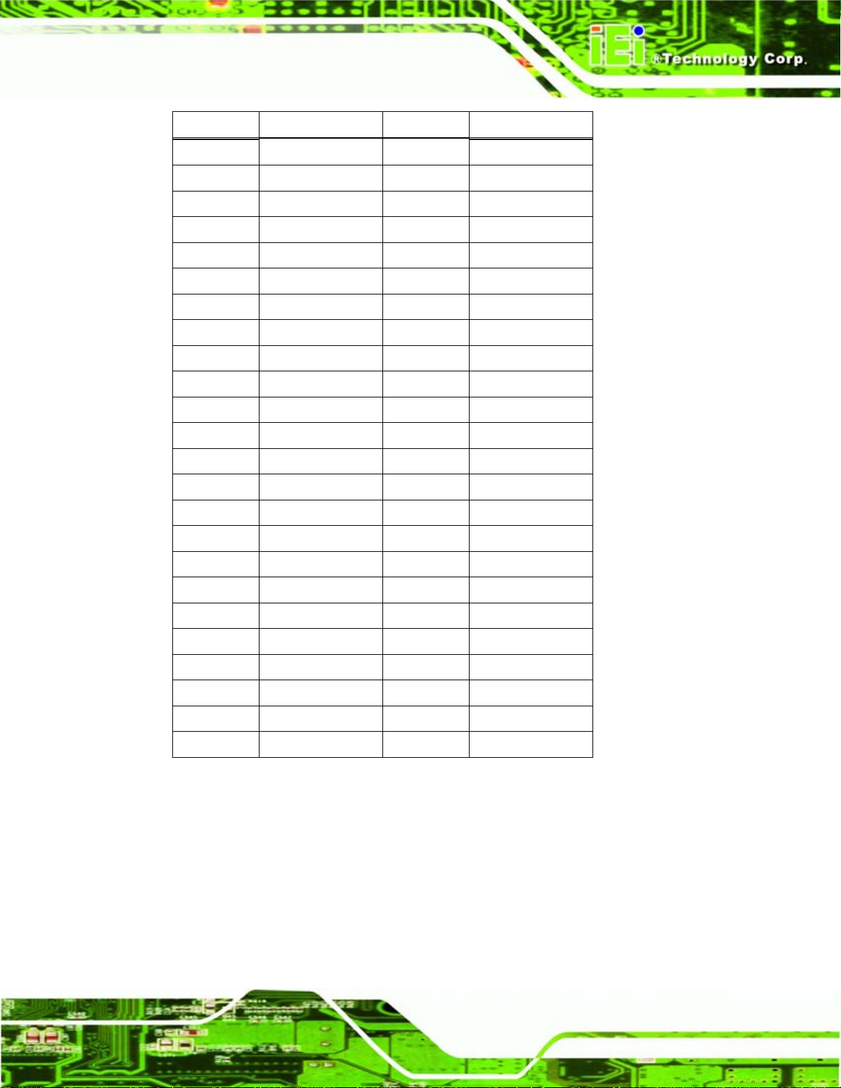
CN Label: AUDIO1
PCIE-9152 PCIMG 1.3 CPU Card
CN Type:
CN Location:
CN Pinouts:
An optional module can be connected to the 10-pin audio connector to provide the system
with a high quality AC’97 or Azalia compatible codec that provides a complete integrated
audio solution.
10-pin header
Figure 4-2
See
Table 4-3
See
Page 30
Figure 4-2: Audio Connector Pinouts (10-pin)
Page 47

PCIE-9152 PCIMG 1.3 CPU Card
PIN NO. DESCRIPTION PIN NO. DESCRIPTION
1 AC97_SYNC 2 AC97_BITCLK
3 AC97_SDOUT 4 AC97_PCBEEP
5 AC97_SDIN 6 AC97_RST#
7 AC97_VCC 8 AC97_GND
9 AC97_12 V 10 AC97_GND
Table 4-3: Audio Connector Pinouts (10-pin)
4.2.2 Backlight Inverter Connector
CN Label: INVERTER1
CN Type:
CN Location:
CN Pinouts:
6-pin wafer (1x6)
Figure 4-3
See
Table 4-4
See
The backlight inverter connector provides the backlight on the LCD display connected to
the PCIE-9152 with +12 V of power.
Figure 4-3: Panel Backlight Connector Pinout Locations
PIN NO. DESCRIPTION
1 +12 V
Page 31
Page 48

PIN NO. DESCRIPTION
2 +12 V
3 BACKLIGHT ENABLE
4 BACKLIGHT ADJUST
5 GROUND
6 GROUND
Table 4-4: Panel Backlight Connector Pinouts
4.2.3 Compact Flash Socket
CN Label: CF1 (solder side)
PCIE-9152 PCIMG 1.3 CPU Card
CN Type:
CN Location:
CN Pinouts:
50-pin header (2x25)
Figure 4-4
See
Table 4-5
See
A CF Type I or Type II memory card is inserted to the CF socket on the solder side of the
PCIE-9152.
Page 32
Figure 4-4: CF Card Socket Location
PIN NO. DESCRIPTION PIN NO. DESCRIPTION
1 GROUND 26 VCC-IN CHECK1
Page 49
PCIE-9152 PCIMG 1.3 CPU Card
PIN NO. DESCRIPTION PIN NO. DESCRIPTION
2 DATA 3 27 DATA 11
3 DATA 4 28 DATA 12
4 DATA 5 29 DATA 13
5 DATA 6 30 DATA 14
6 DATA 7 31 DATA 15
7 HDC_CS0# 32 HDC_CS1
8 N/C 33 N/C
9 GROUND 34 IOR#
10 N/C 35 IOW#
11 N/C 36 VCC_COM
12 N/C 37 IRQ15
13 VCC_COM 38 VCC_COM
14 N/C 39 CSEL
15 N/C 40 N/C
16 N/C 41 HDD_RESET
17 N/C 42 IORDY
18 SA2 43 SDREQ
19 SA1 44 SDACK#
20 SA0 45 HDD_ACTIVE#
21 DATA 0 46 66DET
22 DATA 1 47 DATA 8
23 DATA 2 48 DATA 9
24 N/C 49 DATA 10
25 VCC-IN CHECK2 50 GROUND
Table 4-5: CF Card Socket Pinouts
4.2.4 Fan Connector
CN Label: CPU_FAN1, SYS_FAN1
CN Type:
CN Location:
3-pin header
Figure 4-5
See
Page 33
Page 50

See
CN Pinouts:
Two cooling fan connectors provide a 12 V, 500mA current to a system cooling fan and a
CPU cooling fan. The connector has a "rotation" pin to get rotation signals from fans and
notify the system so the system BIOS can recognize the fan speed. Please note that only
specified fans can issue the rotation signals.
Table 4-6
PCIE-9152 PCIMG 1.3 CPU Card
Figure 4-5: +12 V Fan Connector Location
PIN NO. DESCRIPTION
1 GND
2 +12 V
3 Speed Detect
Table 4-6: +12 V Fan Connector Pinouts
4.2.5 Floppy Disk Connector
CN Label: FDD1
CN Type:
CN Location:
CN Pinouts:
34-pin box header (2x17)
Figure 4-6
See
Table 4-7
See
Page 34
The floppy disk connector is connected to a floppy disk drive.
Page 51
PCIE-9152 PCIMG 1.3 CPU Card
Figure 4-6: 34-pin FDD Connector Location
PIN NO. DESCRIPTION PIN NO. DESCRIPTION
1 GND 2 REDUCE WRITE
3 GND 4 N/C
5 N/C 6 N/C
7 GND 8 INDEX#
9 GND 10 MOTOR ENABLE A#
11 GND 12 DRIVE SELECT B#
13 GND 14 DRIVE SELECT A#
15 GND 16 MOTOR ENABLE B#
17 GND 18 DIRECTION#
19 GND 20 STEP#
21 GND 22 WRITE DATA#
23 GND 24 WRITE GATE#
25 GND 26 TRACK 0#
27 GND 28 WRITE PROTECT#
29 GND 30 READ DATA#
31 GND 32 SIDE 1 SELECT#
33 GND 34 DISK CHANGE#
Table 4-7: 34-pin FDD Connector Pinouts
Page 35
Page 52

4.2.6 GPIO Connector
CN Label: DIO1
PCIE-9152 PCIMG 1.3 CPU Card
CN Type:
CN Location:
CN Pinouts:
The GPIO connector can be connected to external I/O control devices including sensors,
lights, alarms and switches.
10-pin header (2x5)
Figure 4-7
See
Table 4-8
See
Figure 4-7: GPIO Connector Pinout Locations
PIN NO. DESCRIPTION PIN NO. DESCRIPTION
1 GND 2 +5 V
3 GP0 4 GP1
5 GP2 6 GP3
7 GP4 8 GP5
9 GP6 10 GP7
Table 4-8: GPIO Connector Pinouts
4.2.7 Front Panel Connector
CN Label: CN1
CN Type:
12-pin header (2x6)
Page 36
Page 53

PCIE-9152 PCIMG 1.3 CPU Card
See
CN Location:
CN Pinouts:
Figure 4-8
Table 4-9
See
The front panel connector connects to external switches and indicators to monitor and
controls the motherboard. These indicators and switches include:
Power button
Reset button
Power LED
HDD LED
Figure 4-8: Front Panel Connector Pinout Locations
FUNCTION PIN DESCRIPTION FUNCTION PIN DESCRIPTION
Power LED 1 LED+ Buzzer 2 BUZZER 3 LED- 4 NC
Power 5 Power+ 6 NC
Button 7 Power- 8 VCC
HDD LED 9 HDD LED+ Reset 10 RESET
11 HDD LED- 12 GND
Table 4-9: Front Panel Connector Pinouts
Page 37
Page 54
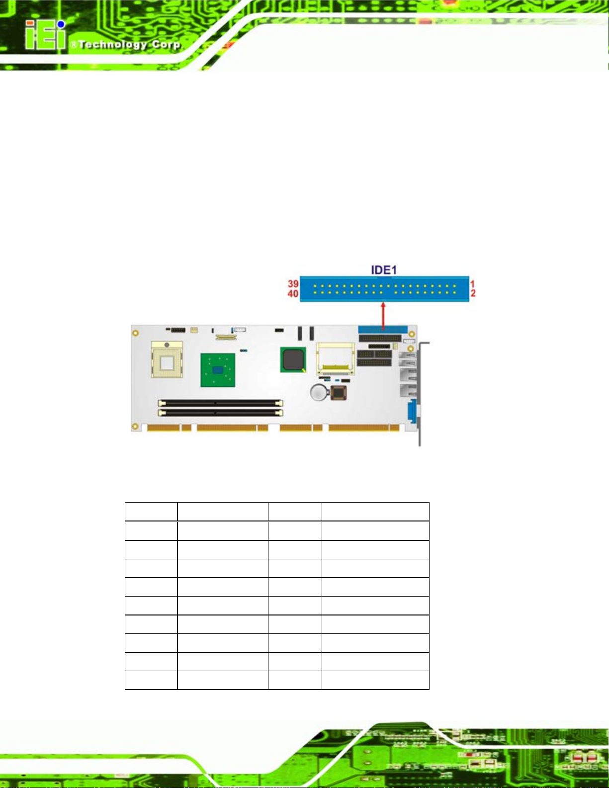
4.2.8 IDE Connector
CN Label: IDE1
PCIE-9152 PCIMG 1.3 CPU Card
CN Type:
CN Location:
CN Pinouts:
40-pin box header (2x20)
Figure 4-9
See
Table 4-10
See
One 40-pin IDE device connector on the PCIE-9152 supports connectivity to two hard disk
drives.
Figure 4-9: Secondary IDE Device Connector Locations
PIN NO. DESCRIPTION PIN NO. DESCRIPTION
1 RESET# 2 GROUND
3 DATA 7 4 DATA 8
5 DATA 6 6 DATA 9
7 DATA 5 8 DATA 10
9 DATA 4 10 DATA 11
11 DATA 3 12 DATA 12
13 DATA 2 14 DATA 13
15 DATA 1 16 DATA 14
17 DATA 0 18 DATA 15
Page 38
Page 55

PCIE-9152 PCIMG 1.3 CPU Card
PIN NO. DESCRIPTION PIN NO. DESCRIPTION
19 GROUND 20 N/C
21 IDE DRQ 22 GROUND
23 IOW# 24 GROUND
25 IOR# 26 GROUND
27 IDE CHRDY 28 GROUND
29 IDE DACK 30 GROUND–DEFAULT
31 INTERRUPT 32 N/C
33 SA1 34 N/C
35 SA0 36 SA2
37 HDC CS0# 38 HDC CS1#
39 HDD ACTIVE# 40 GROUND
Table 4-10: Secondary IDE Connector Pinouts
4.2.9 Infrared Interface Connector
CN Label: IR1
CN Type:
CN Location:
CN Pinouts:
The infrared interface connector supports both Serial Infrared (SIR) and Amplitude Shift
Key Infrared (ASKIR) interfaces.
5-pin header (1x5)
Figure 4-10
See
Table 4-11
See
Page 39
Page 56
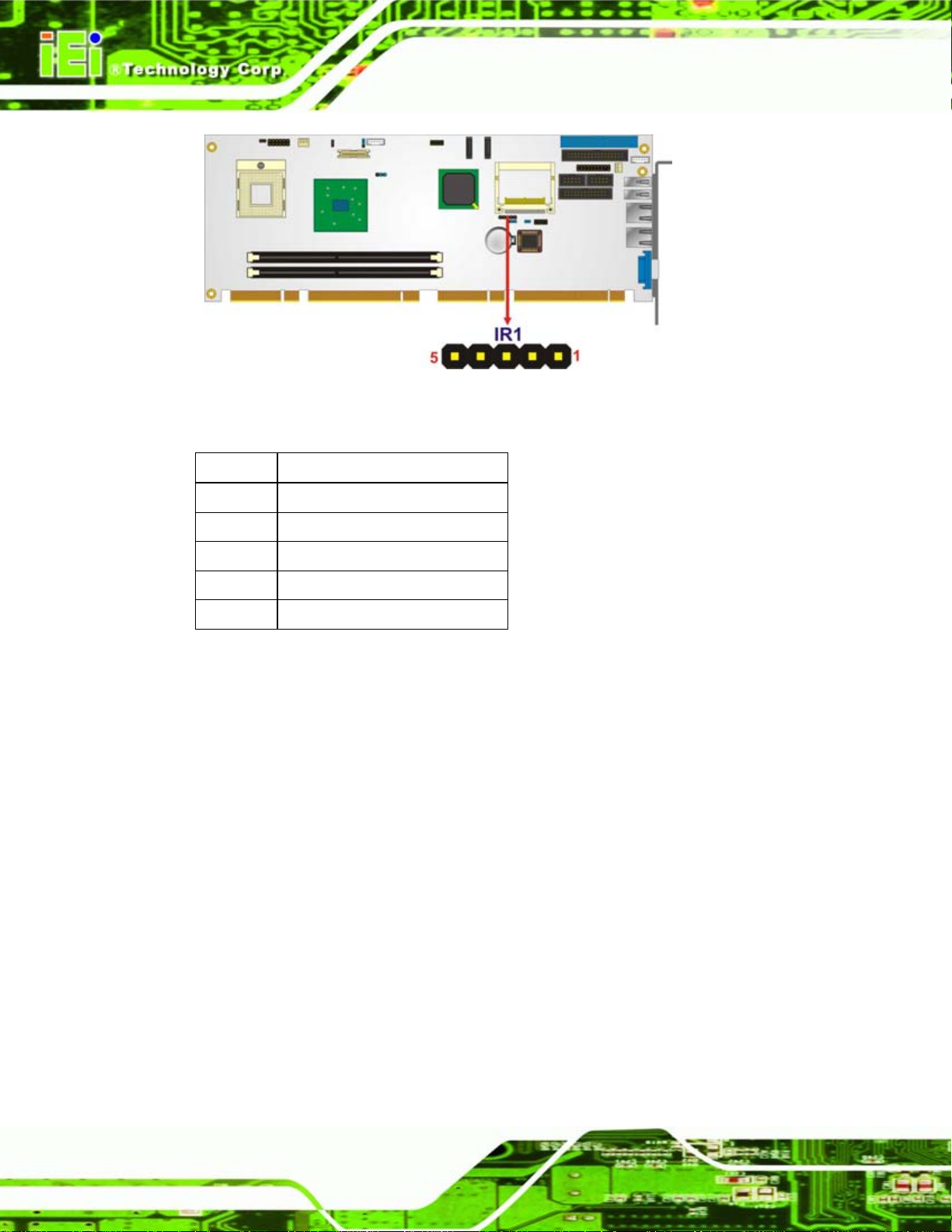
PCIE-9152 PCIMG 1.3 CPU Card
Figure 4-10: Infrared Connector Pinout Locations
PIN NO. DESCRIPTION
1 VCC
2 NC
3 IR-RX
4 GND
5 IR-TX
Table 4-11: Infrared Connector Pinouts
4.2.10 Keyboard and Mouse Connector
CN Label: KB_MS1
CN Type:
CN Location:
CN Pinouts:
The keyboard and mouse connector is for a PS/2 keyboard and mouse.
6-pin header (1x5)
Figure 4-11
See
Table 4-12
See
Page 40
Page 57
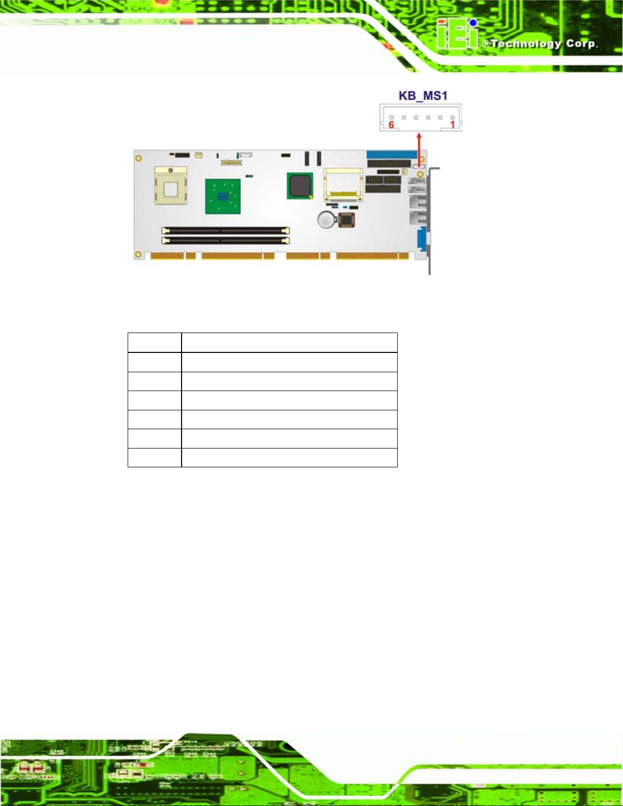
PCIE-9152 PCIMG 1.3 CPU Card
Figure 4-11: Keyboard and Mouse Connector Location
PIN NO. DESCRIPTION
1 5 V
2 Mouse data
3 Mouse clock
4 Keyboard data
5 Keyboard clock
6 Ground
Table 4-12: Keyboard and Mouse Connector Pinouts
4.2.11 LVDS LCD Connector
CN Label: LVDS1
CN Type:
CN Location:
CN Pinouts:
The 30-pin LVDS LCD connector can be connected to single channel or dual channel,
30-pin crimp (2x10)
Figure 4-12
See
Table 4-13
See
24-bit LVDS panel.
Page 41
Page 58

PCIE-9152 PCIMG 1.3 CPU Card
Figure 4-12: LVDS LCD Connector Pinout Locations
PIN NO. DESCRIPTION PIN NO. DESCRIPTION
1 GROUND 2 GROUND
3 LVDSA_Y0+ 4 LVDSA_Y05 LVDSA_Y1+ 6 LVDSA_Y17 LVDSA_Y2+ 8 LVDSA_Y29 LVDSA_CLK+ 10 LVDSA_CLK11 NC 12 NC
13 GROUND 14 GROUND
15 LVDSB_Y0+ 16 LVDSB_Y017 LVDSB_Y1+ 18 LVDSB_Y119 LVDSB_Y2+ 20 LVDSB_Y221 LVDSB_CLK+ 22 LVDSB_CLK23 NC 24 NC
25 GROUND 26 GROUND
27 VCC_LVDS 28 VCC_LVDS
29 VCC_LVDS 30 VCC_LVDS
Table 4-13: LVDS LCD Port Connector Pinouts
Page 42
Page 59

PCIE-9152 PCIMG 1.3 CPU Card
4.2.12 Parallel Port Connector
CN Label: LPT1
CN Type:
CN Location:
CN Pinouts:
26-pin box header
Figure 4-13
See
Table 4-14
See
The 26-pin parallel port connector connects to a parallel port connector interface or some
other parallel port device such as a printer.
Figure 4-13: Parallel Port Connector Location
PIN NO. DESCRIPTION PIN NO. DESCRIPTION
1 STROBE# 2 DATA 0
3 DATA 1 4 DATA 2
5 DATA 3 6 DATA 4
7 DATA 5 8 DATA 6
9 DATA 7 10 ACKNOWLEDGE
11 BUSY 12 PAPER EMPTY
13 PRINTER SELECT 14 AUTO FORM FEED #
15 ERROR# 16 INITIALIZE
17 PRINTER SELECT LN# 18 GROUND
Page 43
Page 60

PIN NO. DESCRIPTION PIN NO. DESCRIPTION
19 GROUND 20 GROUND
21 GROUND 22 GROUND
23 GROUND 24 GROUND
25 GROUND 26 NC
Table 4-14: Parallel Port Connector Pinouts
4.2.13 SATA Drive Connectors
CN Label: SATA1 and SATA3
PCIE-9152 PCIMG 1.3 CPU Card
CN Type:
CN Location:
CN Pinouts:
7-pin SATA drive connectors
Figure 4-14
See
Table 4-15
See
The two SATA drive connectors are each connected to a SATA drive. SATA drives
transfer data at speeds as high as 150 Mb/s.
Page 44
Figure 4-14: SATA Drive Connector Locations
PIN NO. DESCRIPTION
1 GND
2 TX+
Page 61

PCIE-9152 PCIMG 1.3 CPU Card
PIN NO. DESCRIPTION
3 TX4 GND
5 RX6 RX+
7 GND
Table 4-15: SATA Drive Connector Pinouts
4.2.14 SDVO Connector
CN Label: SDVO1
CN Type:
CN Location:
CN Pinouts:
3-pin header (1x3)
Figure 4-15
See
Table 4-16
See
The SDVO connector is connected to and SDVO graphics card inst alled on the backplane.
Figure 4-15: SDVO Connector Pinout Locations
PIN NO. DESCRIPTION
1 NC
Page 45
Page 62

PIN NO. DESCRIPTION
2 SDVO CLK
3 SDVO DATA
Table 4-16: SDVO Pinouts
4.2.15 Serial Port Connector (COM1 & COM2)
CN Label: COM1 & COM2
PCIE-9152 PCIMG 1.3 CPU Card
CN Type:
CN Location:
CN Pinouts:
10-pin header (2x5)
Figure 4-16
See
Table 4-17
See
The 10-pin serial port connector provides a second RS-232 serial communications
channel. The serial port connectors can be connected to external RS-232 serial port
devices.
Page 46
Figure 4-16: COM1 and COM2 Connector Pinout Locations
PIN NO. DESCRIPTION PIN NO. DESCRIPTION
1 Data Carrier Detect (DCD) 6 Data Set to Ready (DSR)
2 Receive Data (RXD ) 7 Request to Send (RTS)
3 Transmit Data (TXD) 8 Clear to Sent (CTS)
4 Data Terminal Ready (DTR) 9 Ring Ind icator (RI)
Page 63

PCIE-9152 PCIMG 1.3 CPU Card
PIN NO. DESCRIPTION PIN NO. DESCRIPTION
5 Ground (GND) 10 5 V
Table 4-17: COM1 and COM2
4.2.16 TPM Connector
CN Label: TPM1
CN Type:
CN Location:
CN Pinouts:
20-pin header (2x10)
See Error! Reference source not found.
See Error! Reference source not found.
The Trusted Platform Module (TPM) connector secures the system on bootup.
Figure 4-17: TPM Connector Pinout Locations
PIN NO. DESCRIPTION PIN NO. DESCRIPTION
1 LCLK 2 GND2
3 LFRAME# 4 KEY
5 LRESET# 6 +5 V
7 LAD3 8 LAD2
9 +3 V 10 LAD1
11 LAD0 12 GND3
13 SCL 14 SDA
Page 47
Page 64

PIN NO. DESCRIPTION PIN NO. DESCRIPTION
15 SB3 V 16 SERIRQ
17 GND1 18 GLKRUN#
19 LPCPD# 20 LDRQ#
PCIE-9152 PCIMG 1.3 CPU Card
Table 4-18: TPM Connector Pinouts
4.3 External Peripheral Interface Connector Panel
Figure 4-18 shows the PCIE-9152 rear panel. The PCIE-9152 rear panel consists of two
RJ-45 Ethernet connectors, a PS/2 keyboard connector a USB port and a VGA connector.
These connectors are accessible when the PCIE-9152 is installed in a chassis.
Figure 4-18: PCIE-9152 External Peripheral Interface Connector
4.3.1 LAN Connectors
CN Label: LAN1 and LAN2
CN Type:
CN Location:
CN Pinouts:
The PCIE-9152 is equipped with two built-in GbE Ethernet controllers. The controllers can
connect to the LAN through two RJ-45 LAN connectors. There are two LEDs on the
connector indicating the status of LAN. The pin assignments are listed in the following
table:
PIN DESCRIPTION PIN DESCRIPTION
1 TXA+ 5 TXC-
RJ-45
Figure 4-18
See
Table 4-19
See
Page 48
2 TXA- 9 TXB3 TXB+ 10 TXD+
Page 65
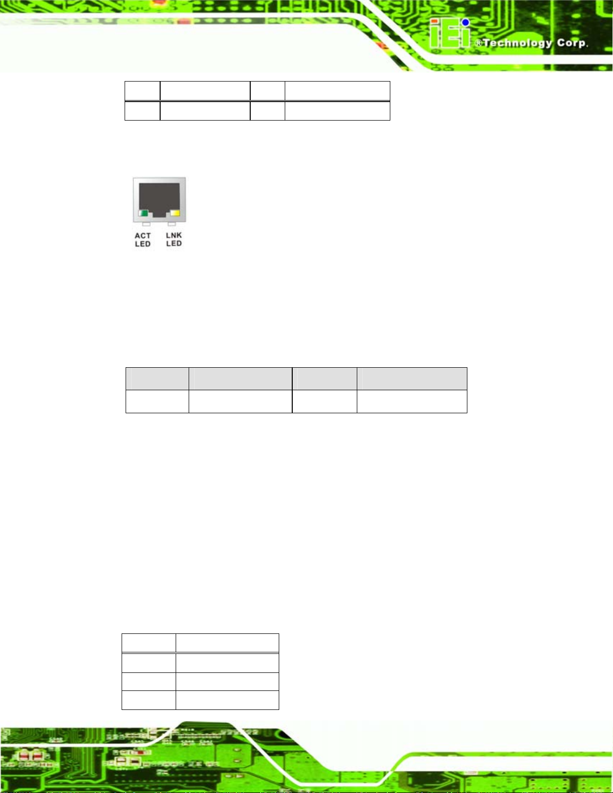
PCIE-9152 PCIMG 1.3 CPU Card
PIN DESCRIPTION PIN DESCRIPTION
4 TXC+ 11 TXD-
Table 4-19: LAN Pinouts
Figure 4-19: RJ-45 Ethernet Connector
The RJ-45 Ethernet connector has two status LEDs, one green and one yello w. The green
LED indicates activity on the port and the yellow LED indicates the port is linked. See
Table 4-20.
Status Description Status Description
Green Activity Yellow Linked
Table 4-20: RJ-45 Ethernet Connector LEDs
4.3.2 USB Connector
CN Label: USB1 and USB2
CN Type:
CN Location:
CN Pinouts:
The PCIE-9152 has a one external USB 2.0 port. The port connects to both USB 2.0 and
USB 1.1 devices.
USB port
Figure 4-18
See
Table 4-21
See
PIN NO. DESCRIPTION
1 VCC
2 DATA3 DATA+
Page 49
Page 66

PIN NO. DESCRIPTION
4 GND
Table 4-21: USB Port Pinouts
4.3.3 VGA Connector
CN Label: VGA1
PCIE-9152 PCIMG 1.3 CPU Card
CN Type:
CN Location:
CN Pinouts:
15-pin Female
Figure 4-18
See
Figure 4-20 and Table 4-22
See
The PCIE-9152 has a single 15-pin female connector for connectivity to standard display
devices.
Figure 4-20: VGA Connector
PIN DESCRIPTION PIN DESCRIPTION
1 RED 2 GREEN
Page 50
3 BLUE 4 NC
5 GND 6 GND
7 GND 8 GND
9 VCC / NC 10 GND
11 NC 12 DDC DAT
13 HSYNC 14 VSYNC
15 DDCCLK
Table 4-22: VGA Connector Pinouts
Page 67

PCIE-9152 PCIMG 1.3 CPU Card
Chapter
5
5 Installation
Page 51
Page 68
5.1 Anti-static Precautions
WARNING:
Failure to take ESD precautions during the installation of the
PCIE-9152 may result in permanent damage to the PCIE-9152 and
severe injury to the user.
Electrostatic discharge (ESD) can cause serious damage to electronic components,
including the PCIE-9152. Dry climates are especially susceptible to ESD. It is therefore
critical that whenever the PCIE-9152, or any other electrical component is handled, the
following anti-static precautions are strictly adhered to.
Wear an anti-static wristband: - Wearing a simple anti-static wristband can
PCIE-9152 PCIMG 1.3 CPU Card
help to prevent ESD from damaging the board.
Self-grounding:- Before handling the board touch any grounded conducting
material. During the time the board is handled, frequently touch any
conducting materials that are connected to the ground.
Use an anti-static pad: When configuring the PCIE-9152, place it on an
antic-static pad. This reduces the possibility of ESD damaging the PCIE-91 52.
Only handle the edges of the PCB:-: When handling the PCB, hold the PCB
by the edges.
5.2 Installation Considerations
NOTE:
The following installation notices and installation considerations should
be read and understood before the PCIE-9152 is installed. All
installation notices pertaining to the installation of the PCIE-9152
Page 52
should be strictly adhered to. Failing to adhere to these precautions
may lead to severe damage of the PCIE-9152 and injury to the person
installing the motherboard.
Page 69
PCIE-9152 PCIMG 1.3 CPU Card
5.2.1 Installation Notices
WARNING:
The installation instructions described in this manual should be
carefully followed in order to prevent damage to the PCIE-9152,
PCIE-9152 components and injury to the user.
Before and during the installation please DO the following:
Read the user manual:
o The user manual provides a complete description of the PCIE-9152
installation instructions and configuration options.
Wear an electrostatic discharge cuff (ESD):
o Electronic components are easily damaged by ESD. Wearing an ESD cuff
removes ESD from the body and helps prevent ESD damage.
Place the PCIE-9152 on an antistatic pad:
o When installing or configuring the motherboard, place it on an antistatic
pad. This helps to prevent potential ESD damage.
Turn all power to the PCIE-9152 off:
o When working with the PCIE-9152, make sure that it is disconnected from
all power supplies and that no electricity is being fed into the system.
Before and during the installation of the PCIE-9152 DO NOT:
Do Not: Remove any of the stickers on the PCB board. These stickers are
required for warranty validation.
Do Not: Use the product before verifying all the cables and power connectors
are properly connected.
Do Not: Allow screws to come in contact with the PCB circuit, connector pins,
or its components.
5.2.2 Installation Checklist
The following checklist is provided to ensure the PCIE-9152 is properly installed.
Page 53
Page 70

All the items in the packing list are present
The CPU is installed
The CPU cooling kit is properly installed
A compatible memory module is properly inserted into the slot
The CF Type I or CF Type II card is properly installed into the CF socket
The jumpers have been properly configured
The PCIE-9152 is inserted into a chassis with adequate ventilation
The correct power supply is being used
The following devices are properly connected
PCIE-9152 PCIMG 1.3 CPU Card
o IDE device
o SATA drives
o Keyboard and mouse cable
o Audio kit
o Power supply
o USB cable
o Serial port cable
o Parallel port cable
The following external peripheral devices are properly connected to the
chassis:
o VGA screen
o USB device
o LAN connection
5.3 CPU, CPU Cooling Kit and DIMM Installation
WARNING:
A CPU should never be turned on without the specified cooling kit
being installed. If the cooling kit (heat sink and fan) is not properly
installed and the system turned on, permanent damage to the CPU,
PCIE-9152 and other electronic components attached to the system
Page 54
may be incurred. Running a CPU without a cooling kit may also result
in injury to the user.
Page 71
PCIE-9152 PCIMG 1.3 CPU Card
The CPU, CPU cooling kit and DIMM are the most critical components of the PCIE-9152.
If one of these component is not installed the PCIE-9152 cannot run.
5.3.1 Socket 479 CPU Installation
The CPU installation only applies to models that have a Socket 479 CPU socket. Skip the
CPU installation for models that have the CPU preinstalled.
If a CPU is not preinstalled on the PCIE-9152, please follow the installation instructions
below.
WARNING:
CPUs are expensive and sensitive components. When installing the
CPU please be careful not to damage it in anyway. Make sure the CPU
is installed properly and ensure the correct cooling kit is properly
installed.
To install a socket 479 CPU onto the PCIE-9152, follow the steps below:
WARNING:
When handling the CPU, only hold it on the sides. DO NOT touch the
pins at the bottom of the CPU.
Step 1: Unlock the CPU retention screw. When shipped, the retention screw of the
CPU socket should be in the unlocked position. If it is not in the unlocked
position, use a screwdriver to unlock the screw. See
Figure 5-1.
Page 55
Page 72
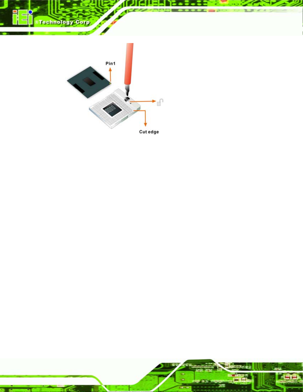
Figure 5-1: Make sure the CPU socket retention screw is unlocked
Step 2: Inspect the CPU socket. Make sure there are no bent pins an d make sure the
PCIE-9152 PCIMG 1.3 CPU Card
socket contacts are free of foreign material. If any debris is found, remove it with
compressed air.
Step 3: Correctly Orientate the CPU. Make sure the IHS (integrated heat sink) side is
facing upwards.
Step 4: Correctly position the CPU. Match the Pin 1 mark with the cut edge on the
CPU socket. See
Step 5: Align the CPU pins. Carefully align the CPU pins with the holes in the CPU
socket.
Step 6: Insert the CPU. Gently insert the CPU into the socket. If the CPU pins are
properly aligned, the CPU should slide into the CPU socket smoothly.
Step 7: Lock the retention screw. Rotate the retention screw into the locked position.
Figure 5-2. Step 7:
See
Figure 5-1.
Page 56
Page 73
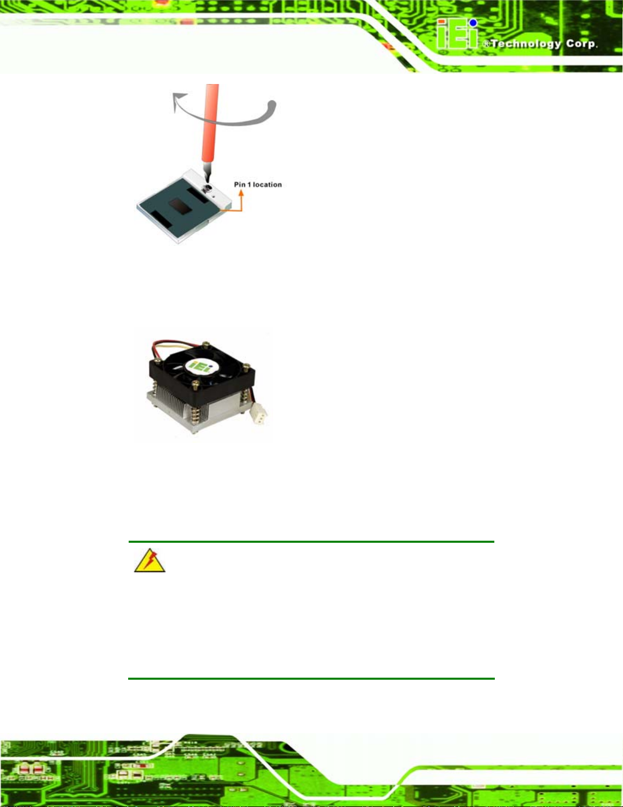
PCIE-9152 PCIMG 1.3 CPU Card
Figure 5-2: Lock the CPU Socket Retention Screw
5.3.2 Cooling Kit Installation
Figure 5-3: Cooling Kit
An IEI Socket 479 CPU cooling kit can be purchased separately. The cooling kit
comprises a CPU heat sink and a cooling fan.
WARNING:
Do not wipe off (accidentally or otherwise) the pre-sprayed layer of
thermal paste on the bottom of the heat sink. The thermal paste
between the CPU and the heat sink is important for optimum heat
dissipation.
To install the cooling kit, please follow the steps below.
Page 57
Page 74

Step 8: Place the cooling kit onto the CPU. Make sure the CPU cooling fan cable
can be properly routed when the cooling kit is install ed.
Step 9: Properly align the cooling kit. Make sure its four spring screw fasteners can
pass through the pre-drilled holes on the PCB.
Step 10: Secure the cooling kit. From the solder side of the PCB, align the support
bracket to the screw threads on heat sink that were inserted through the PCB
PCIE-9152 PCIMG 1.3 CPU Card
holes. (See
Figure 5-4: Cooling Kit Support Bracket
Step 11: Tighten the screws. Use a screwdriver to tighten the four screws. Tighten each
nut a few turns at a time and do not over-tighten the screws.
Figure 5-4)
Page 58
Step 12: Connect the fan cable. Connect the cooling kit fan cable to the fan connector
on the motherboard. Carefully route the cable and avoid heat generating chips
and fan blades. See
Figure 5-5. Step 12:
Page 75

PCIE-9152 PCIMG 1.3 CPU Card
Figure 5-5: Connect the cooling fan cable
5.3.3 DIMM Installation
WARNING:
Using incorrectly specified DIMM may cause permanently damage the
PCIE-9152. Please make sure the purchased DIMM complies with the
memory specifications of the PCIE-9152. DIMM specifications
compliant with the PCIE-9152 are listed in Chapter 2.
To install a DIMM into a DIMM socket, please follow the steps below and refer to
Figure 5-6.
Page 59
Page 76

Figure 5-6: Installing a DIMM
PCIE-9152 PCIMG 1.3 CPU Card
Step 13: Open the DIMM socket handles. The DIMM socket has two handles that
secure the DIMM into the socket. Before the DIMM can be inserted into the
socket, the handles must be opened. See
Step 14: Align the DIMM with the socket. The DIMM must be oriented in such a way
that the notch in the middle of the DIMM must be aligned with the plastic bridge
in the socket. See
Step 15: Insert the DIMM. Once properly aligne d, the DIMM can be inserted into the
socket. As the DIMM is inserted, the white handles on the side of the socket will
close automatically and secure the DIMM to the socket. See
Step 16: Removing a DIMM. To remove a DIMM, push both handles outward. The
memory module is ejected by a mechanism in the socket.Step 0:
Figure 5-6.
Figure 5-6.
Figure 5-6.
Page 60
Page 77

PCIE-9152 PCIMG 1.3 CPU Card
5.3.4 CF Card Installation
NOTE:
The PCIE-9152 can support both CF Type I cards and CF Type II
cards. For the complete specifications of the supported CF cards
please refer to Chapter 2.
To install the a CF card (Type 1 or Type 2) onto the PCIE-9152, please follow the steps
below:
Step 1: Locate the CF card socket. Place the PCIE-9152 on an anti-static pad with the
solder side facing up. Locate the CF card.
Step 2: Align the CF card. Make sure the CF card is properly aligned with the CF
socket.
Step 3: Insert the CF card. Gently insert the CF card into the socket making sure the
socket pins are properly inserted into the socket. See
Figure 5-7. Step 3:
Figure 5-7: CF Card Installation
Page 61
Page 78

5.4 Jumper Settings
NOTE:
A jumper is a metal bridge used to close
an electrical circuit. It consists of two or
three metal pins and a small metal clip
(often protected by a plastic cover) that
slides over the pins to connect them. To
CLOSE/SHORT a jumper means
connecting the pins of the jumper with
the plastic clip and to OPEN a jumper means removing the plastic clip
from a jumper.
PCIE-9152 PCIMG 1.3 CPU Card
Before the PCIE-9152 is installed in the system, the jumpers must be set in accordance
with the desired configuration. The jumpers on the PCIE-9152 are listed in
Description Label Type
CF card setup JP5 2-pin header
Clear CMOS JP1 3-pin header
FSB Selection JP3 3-pin header
LVDS voltage selection JP2 3-pin header
Table 5-1: Jumpers
Table 5-1.
5.4.1 CF Card Setup
Jumper Label: JP5
Jumper Type:
Jumper Settings:
2-pin header
Table 5-2
See
Page 62
Jumper Location:
Figure 5-8
See
Page 79

PCIE-9152 PCIMG 1.3 CPU Card
The CF Card Setup jumper sets the CF Type I card or CF Type II cards as either the slave
device or the master device. CF Card Setup jumper settings are shown in
AT Power Select Description
Open Slave Default
Close Master
Table 5-2: CF Card Setup Jumper Settings
The CF Card Setup jumper location is shown in Figure 5-8.
Table 5-2.
Figure 5-8: CF Card Setup Jumper Location
5.4.2 Clear CMOS Jumper
Jumper Label: JP1
Jumper Type:
Jumper Settings:
Jumper Location:
3-pin header
Table 5-3
See
Figure 5-9
See
Page 63
Page 80
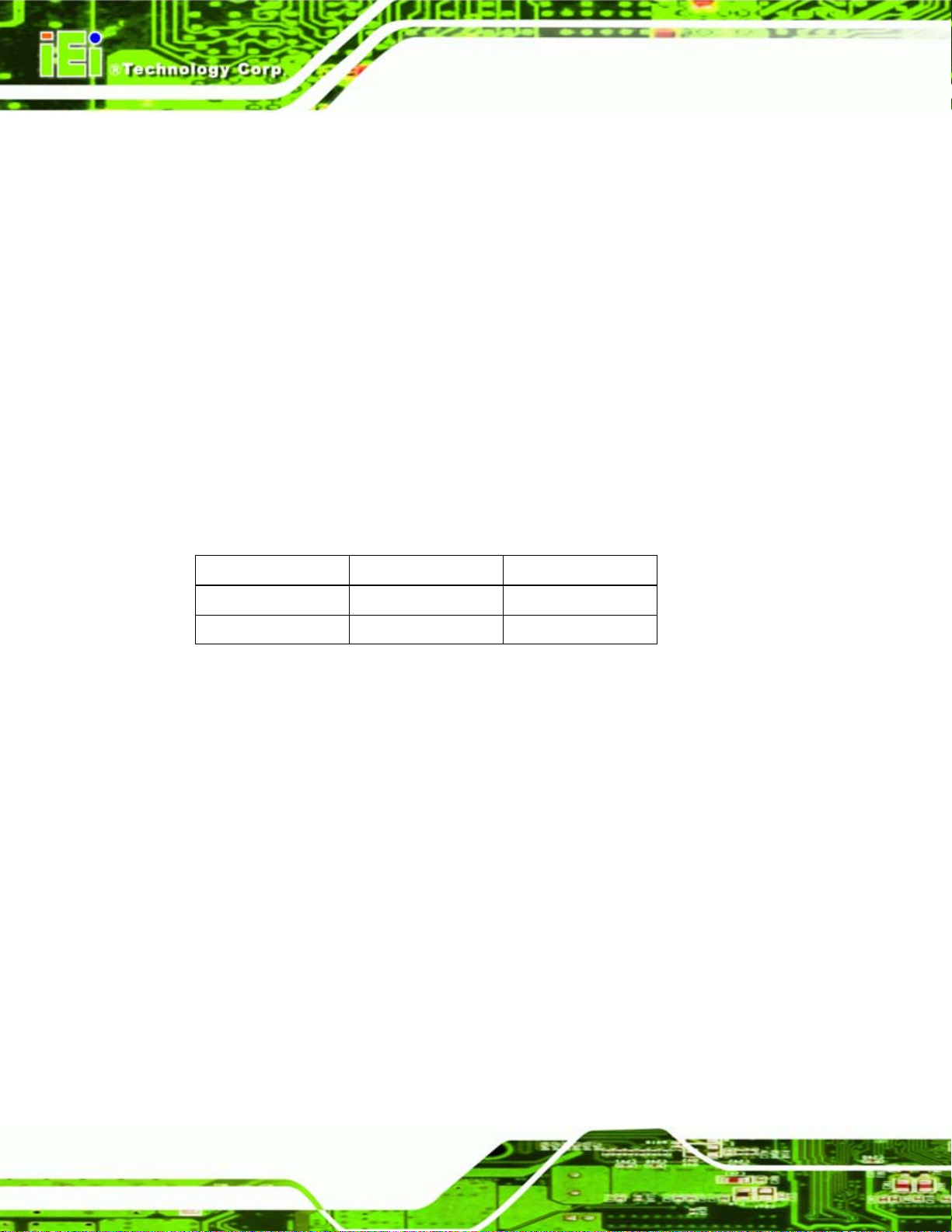
If the PCIE-9152 fails to boot due to improper BIOS settings, the clear CMOS jumper
clears the CMOS data and resets the system BIOS information. To do this, use the jumper
cap to close pins 2 and 3 for a few seconds then reinstall the jumper clip back to pins 1
and 2.
If the “CMOS Settings Wrong” message is displayed during the boot up process, the fault
may be corrected by pressing the F1 to enter the CMOS Setup menu. Do one of the
following:
Enter the correct CMOS setting
Load Optimal Defaults
Load Failsafe Defaults.
After having done one of the above, save the changes and exit the CMOS Setup menu.
PCIE-9152 PCIMG 1.3 CPU Card
The clear CMOS jumper settings are shown in
AT Power Select Description
Short 1 - 2 Keep CMOS Setup Default
Short 2 – 3 Clear CMOS Setup
Table 5-3: Clear CMOS Jumper Settings
The location of the clear CMOS jumper is shown in Figure 5-9 below.
Table 5-3.
Page 64
Page 81

PCIE-9152 PCIMG 1.3 CPU Card
Figure 5-9: Clear CMOS Jumper
5.4.3 FSB Setup Jumper
Jumper Label: JP3
Jumper Type:
Jumper Settings:
Jumper Location:
The clear FSB setup jumper enables a user to select the FSB speed on the PCIE-9152.
The FSB Setup jumper settings are shown in
FSB Setup Description
Short 1 – 2 100 MHz Default
Short 2 – 3 133 MHz
3-pin header
Table 5-4
See
Figure 5-10
See
Table 5-3.
Table 5-4: FSB Setup Jumper Settings
The location of the FSB Setup jumper is shown in Figure 5-9 below.
Page 65
Page 82
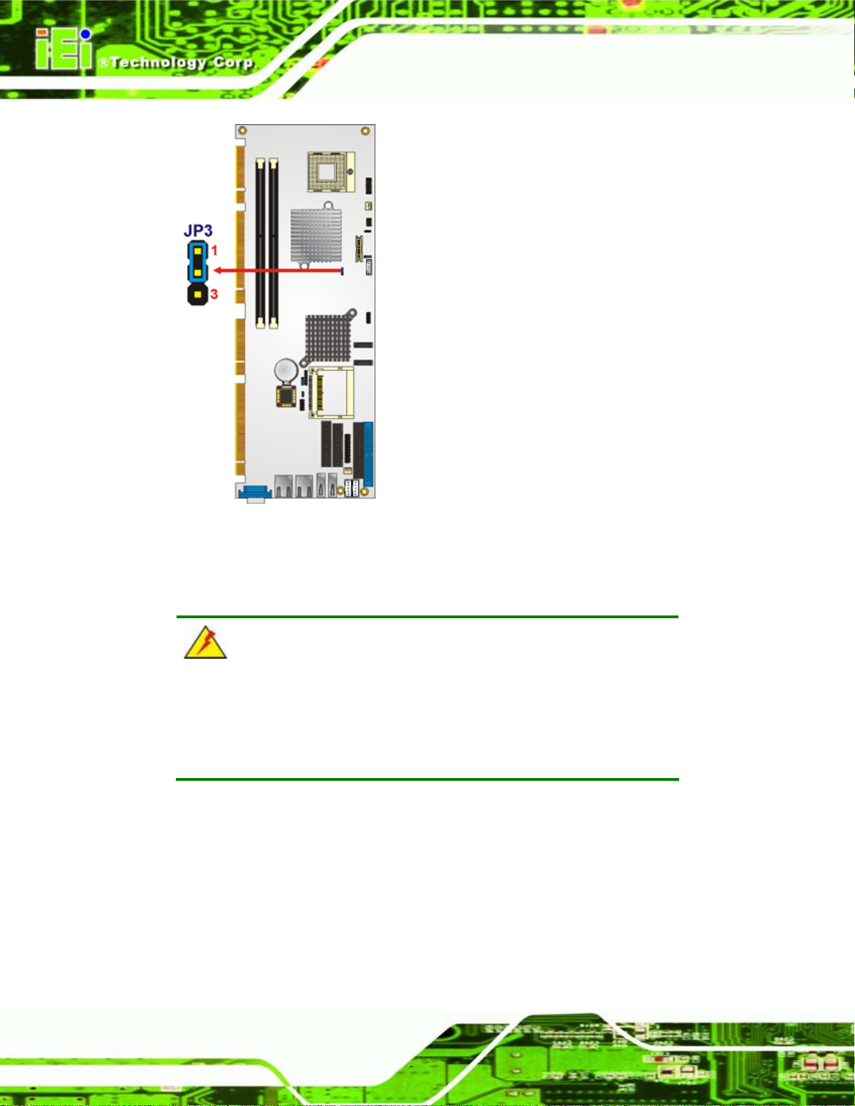
PCIE-9152 PCIMG 1.3 CPU Card
Figure 5-10: FSB Setup Jumper Jumper
5.4.4 LVDS Voltage Selection
WARNING:
Permanent damage to the screen and PCIE-9152 may occur if the
wrong voltage is selected with this jumper. Please refer to the user
guide that cam with the monitor to select the correct voltage.
Jumper Label: JP2
Jumper Type:
Jumper Settings:
3-pin header
Table 5-5
See
Page 66
Figure 5-11
Jumper Location:
The LVDS Voltage Selection jumper allows the LVDS screen voltage to be set. The
LVDS Voltage Selection jumper settings are shown in
See
Table 5-5.
Page 83

PCIE-9152 PCIMG 1.3 CPU Card
AT Power Select Description
Short 1-2 +3.3 V LVDS Default
Short 2-3 +5 V LVDS
Table 5-5: LVDS Voltage Selection Jumper Settings
The LVDS Voltage Selection jumper location. is shown in Figure 5-11.
Figure 5-11: LVDS Voltage Selection Jumper Pinout Locations
5.5 Chassis Installation
5.5.1 Airflow
WARNING:
Airflow is critical to the cooling of the CPU and other onboard
components. The chassis in which the PCIE-9152 must have air vents
to allow cool air to move into the system and hot air to move out.
Page 67
Page 84
The PCIE-9152 must be installed in a chassis with ventilation holes on the sides allowing
airflow to travel through the heat sink surface. In a system with an individual power supply
unit, the cooling fan of a power supply can also help generate airflow through the board
surface.
NOTE:
IEI has a wide range of backplanes available. Please contact your
PCIE-9152 vendor, reseller or an IEI sales representative at
sales@iei.com.tw or visit the IEI website (http://www.ieiworld.com.tw)
to find out more about the available chassis.
5.5.2 Backplane Installation
PCIE-9152 PCIMG 1.3 CPU Card
Before the PCIE-9152 can be installed into the chassis, a backplane must first be
installed. Please refer to the installation instructions that came with the backplane and the
chassis to see how to install the backplane into the chassis.
NOTE:
IEI has a wide range of backplanes available. Please contact your
PCIE-9152 vendor, reseller or an IEI sales representative at
sales@iei.com.tw or visit the IEI website (http://www.ieiworld.com.tw)
to find out more about the available chassis.
5.5.3 CPU Card Installation
To install the PCIE-9152 CPU card onto the backplane, carefully align the CPU card
interface connectors with the corresponding socket on the backplane. To do this, please
refer to the reference material that came with the backplane. Next, secure the CPU card to
Page 68
the chassis. To do this, please refer to the reference material that came with the chassis.
Page 85
PCIE-9152 PCIMG 1.3 CPU Card
5.6 Internal Peripheral Device Connections
5.6.1 Peripheral Device Cables
The cables listed in Table 5-6 are shipped with the PCIE-9152.
Quantity Type
1 IDE Cable
1 KB/MS cable
2 SATA drive cables
1 SATA drive power cable
Table 5-6: IEI Provided Cables
Optional cables are listed below:
LPT cable
FDD cable
5-pin wafer-to-PS/2 cable for mouse or keyboard
7.1 channel audio kit
5.1 channel audio kit
5.6.2 IDE Cable Connection
The IDE flat cable connects to the PCIE-9152 to one or two IDE devices. To connect an
IDE HDD to the PCIE-9152 please follow the instructions below.
Step 4: Locate the IDE connector. The location/s of the IDE device connector/s is/are
shown in Chapter 3..
Step 5: Insert the connector. Connect the IDE cable connector to the onboard
connector. See
can only be inserted in one direction.
Figure 5-12. A key on the front of the cable connector ensures it
Page 69
Page 86

Figure 5-12: IDE Cable Connection
PCIE-9152 PCIMG 1.3 CPU Card
Step 6: Connect the cable to an IDE device. Connect the two connectors on the other
side of the cable to one or two IDE devices. Make sure that pin 1 on the cable
corresponds to pin 1 on the connectorStep 0:
5.6.3 5.1 Channel Audio Kit Installation
NOTE:
This is an optional item that must be ordered separately. For further
information please contact the nearest PCIE-9152 distributor, reseller
or vendor or contact an iEi sales representative directly. Send any
queries to
The optional 5.1 channel audio kit connects to the 10-pin audio connector on the
PCIE-9152. The audio kit consists of three audio jacks. One audio jack, Mic In, connects
to a microphone. The remaining two audio jacks, Line-In and Line-Out, connect to two
sales@iei.com.tw.
Page 70
speakers. To install the audio kit, please refer to the steps below:
Step 1: Connect the audio kit cable. The audio kit is shipped with a cable that
connects the audio kit to the PCIE-9152. Connect the cable to the connector on
Page 87
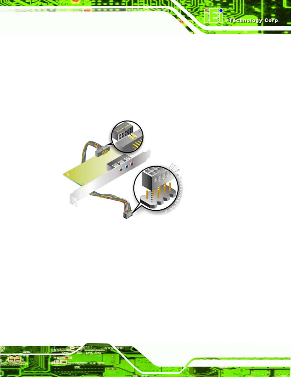
PCIE-9152 PCIMG 1.3 CPU Card
the back of the audio kit. Make sure the pins are properly aligned (i.e. pin 1
connects to pin 1).
Step 2: Locate the audio connector. The location of the 10-pin audi o connector is
shown in Chapter 3.
Step 3: Align pin 1. Align pin 1 on the onboard connector with pin 1 on the audio kit
cable connector. Pin 1 on the audio kit cable connector is indicated with a white
dot. See
Figure 5-13: 5.1 Channel Audio Kit
Step 4: Mount the audio kit onto the chassis. Once the audio kit is connected to the
Figure 5-13.
PCIE-9152, secure the audio kit bracket to the system chassis.
Step 5: Connect the audio devices. Connect one speaker to the line-in audio jack, one
speaker to the line-out audio jack and a microphone to the mic-in audio jack.
Step 6: Install the driver. If the 5.1 channel audio kit is used, the ALC655 Realtek
codec driver must be installed. Refe r t o Chapter 7 for driver installation
instructions.Step 0:
Page 71
Page 88
5.6.4 7.1 Channel Audio Kit Installation
NOTE:
This is an optional item that must be ordered separately. For further
information please contact the nearest PCIE-9152 distributor, reseller
or vendor or contact an iEi sales representative directly. Send any
PCIE-9152 PCIMG 1.3 CPU Card
queries to
The optional 7.1 channel audio kit connects to the 10-pin audio connector on the
PCIE-9152. The audio kit consists of five audio jacks. One audio jack, Mic In, connects to
a microphone. The remaining four audio jacks, Line-In, Front-Out, Rear-Out, and Center
Subwoofer, connect to speakers. To install the audio kit, please refer to the steps below:
Step 1: Connect the audio kit cable. The audio kit is shipped with a cable that
connects the audio kit to the PCIE-9152. Connect the cable to the connector on
the back of the audio kit. Make sure the pins are properly aligned (i.e. pin 1
connects to pin 1).
Step 2: Locate the audio connector. The location of the 10-pin audi o connector is
shown in Chapter 3.
Step 3: Align pin 1. Align pin 1 on the onboard connector with pin 1 on the audio kit
sales@iei.com.tw.
Page 72
cable connector. Pin 1 on the audio kit cable connector is indicated with a white
dot. See
Figure 5-13.
Page 89

PCIE-9152 PCIMG 1.3 CPU Card
Figure 5-14: 5.1 Channel Audio Kit
Step 4: Mount the audio kit onto the chassis. Once the audio kit is connected to the
PCIE-9152, secure the audio kit bracket to the system chassis.
Step 5: Connect the audio devices. Connect one speaker to the line-in audio jack, one
speaker to the line-out audio jack and a microphone to the mic-in audio jack.
Step 6: Install the driver. If the 5.1 channel audio kit is used, the ALC655 Realtek
codec driver must be installed. Refe r t o Chapter 7 for driver installation
instructions.Step 0: Step 0:
5.6.5 FDD Cable Connection
The FDD flat cable connects to the PCIE-9152 to one FDD device. To connect an FDD to
the PCIE-9152 please follow the instructions below.
Step 1: Locate the FDD connector. The location of the FDD device connector i s shown
in Chapter 3.
Page 73
Page 90

Step 2: Insert the connector. Connect the FDD cable connector to the on-board
PCIE-9152 PCIMG 1.3 CPU Card
connector. See
can only be inserted in one direction.
Figure 5-15: FDD Cable Connection
Figure 5-15. A key on the front of the cable connector ensures it
Step 3: Connect the cable to an FDD device. Connect the connector at the other end
of the cable to an FDD device. Make sure that pin 1 on the cable corresponds to
pin 1 on the connector. Step 0:
5.6.6 Parallel Port Cable
The optional parallel port (LPT) cable respectively connects the onboard LPT 26-pin box
header to an external LPT device (like a printer). The cable comprises a 26-pin female
header, to be connected to the onboard LPT box-header, on one side and on the other
side a standard external LPT connector. To connect the LPT cable, please follow the
steps below.
Step 1: Locate the connector. The LPT con nector location is shown in Chapter 4.
Step 2: Align the connectors. Correctly align pin 1 on the cable connector with pin 1 on
the PCIE-9152 LPT box-header connector. See
Figure 5-16.
Page 74
Page 91

PCIE-9152 PCIMG 1.3 CPU Card
Step 3: Insert the cable connectors. Once the cable connector is p rope rly aligne d wit h
the 26-pin box-header connector on the PCIE-9152, connect the cable
connector to the onboard connector. See
Figure 5-16: LPT Cable Connection
Step 4: Attach the LPT connector brack et to the chassis. The LPT cabl e connector is
connected to a standard external LPT interface connector. To secure the LPT
Figure 5-16.
interface connector to the chassis please refer to the installation instructions that
came with the chassis.
Step 5: Connect LPT device. Once the LPT interface connector is co nnected to the
chassis, the LPT device can be connected to the LPT interface connector. See
Figure 5-17Step 5:\
Page 75
Page 92

Figure 5-17: Connect the LPT Device
5.6.7 Dual RS-232 Cable Connection
PCIE-9152 PCIMG 1.3 CPU Card
The dual RS-232 cable consists of two connectors attached to two independent cables.
Each cable is then attached to a D-sub 9 male connector that is mounted onto a bracket.
To install the dual RS-232 cable, please follow the steps below.
Step 6: Locate the connectors. The locations of the RS-232 connectors are sho wn in
Chapter 3.
Step 7: Insert the cable connectors. Insert one connector into each serial port box
headers. See
the connector can only be installed in one direction.
Figure 5-18. A key on the front of the cable connectors ensures
Page 76
Page 93

PCIE-9152 PCIMG 1.3 CPU Card
Figure 5-18: Dual RS-232 Cable Installation
Step 8: Secure the bracket. The dual RS-232 connector has two D-sub 9 male
connectors secured on a bracket. To secure the bracket to the chassis please
refer to the reference material that came with the chassisStep 0:
5.6.8 SATA Drive Connection
The PCIE-9152 is shipped with two SATA drive cables and one SATA drive power cable.
To connect the SATA drives to the connectors, please follow the steps below.
Step 1: Locate the connectors. The locations of the SATA drive connectors are shown
in Chapter 3.
Step 2: Insert the cable connector. Press the clip on the connector at the end of the
SATA cable and insert the cabl e connector into the onboard SATA drive
connector. See
Figure 5-19.
Page 77
Page 94

PCIE-9152 PCIMG 1.3 CPU Card
Figure 5-19: SATA Drive Cable Connection
Step 3: Connect the cable to the SATA disk. Connect the connector on the other end
of the cable to the connector at the back of the SATA drive. See
Step 4: Connect the SATA power cable. Connect the SATA power connector to the
back of the SATA drive. See
Figure 5-20. Step 4:
Figure 5-20.
Page 78
Page 95

PCIE-9152 PCIMG 1.3 CPU Card
Figure 5-20: SATA Power Drive Connection
5.6.9 Dual PS/2 Cable
The dual PS/2 cable connects the keyboard and mouse connector to two PS/2 ports.
Step 5: Locate the connector. The location of the keyboard/mouse conne ctor is shown
in Chapter 4.
Step 6: Align the connector. The plug can only be inserted one way, align pin 1
correctly. See
Step 7: Insert the cable connectors. Push the plug down to engage and secure. See
Figure 5-21.
Figure 5-21.
Page 79
Page 96
PCIE-9152 PCIMG 1.3 CPU Card
Figure 5-21: Keyboard/Mouse Cable Connection
Step 8: Attach PS/2 connector to the chassis. Secure the PS/2 connector at the end
of the cable to the chassis of the computer. The plugs should face outward for
easy installation of a keyboard and mouse.
Step 9: Connect the keyboard or mouse. Once secured to the chassis and keyboard
and mouse can be attached to their respective plugs. Step 0:
5.7 External Peripheral Interface Connection
The following external peripheral devices can be connected to the external peripheral
interface connectors.
VGA monitors
RJ-45 Ethernet cable connectors
Page 80
USB devices
Page 97
PCIE-9152 PCIMG 1.3 CPU Card
To install these devices, connect the corresponding cable connector from the actual
device to the corresponding PCIE-9152 external peripheral interface connector making
sure the pins are properly aligned.
5.7.1 LAN Connection (Single Connector)
There are two external RJ-45 LAN connectors. The RJ-45 connectors enable connection
to an external network. To connect a LAN cable with an RJ-45 connector, please follow
the instructions below.
Step 1: Locate the RJ-45 connectors. The locations of the USB connecto rs are shown
in Chapter 4.
Step 2: Align the connectors. Align the RJ-45 connector on the LAN cable with one of
the RJ-45 connectors on the PCIE-9152. See
Figure 5-22: LAN Connection
Figure 5-22.
Step 3: Insert the LAN cable RJ-45 connector. Once aligned, gently insert the LAN
cable RJ-45 connector into the onboard RJ-45 connector. Step 0:
Page 81
Page 98

PCIE-9152 PCIMG 1.3 CPU Card
5.7.2 USB Device Connection (Single Connector)
There are two external USB 2.0 connectors. Both connectors are perpendicular to the
PCIE-9152. To connect a USB 2.0 or USB 1.1 device, please follow the instructions
below.
Step 1: Located the USB connectors. The locations of the USB connectors are shown
in Chapter 4.
Step 2: Align the connectors. Align the USB device connector with one of the
connectors on the PCIE-9152. See
Figure 5-22.
Page 82
Figure 5-23: USB Device Connection
Step 3: Insert the device connector. Once aligned, gently insert the USB device
connector into the onboard connector. Step 0:
Page 99
PCIE-9152 PCIMG 1.3 CPU Card
5.7.3 VGA Monitor Connection
The PCIE-9152 has a single female DB-15 connector on the external peripheral interface
panel. The DB-15 connector is connected to a CRT or VGA monitor. To connect a monitor
to the PCIE-9152, please follow the instructions below.
Step 1: Locate the female DB-15 connector. The location of the female DB-15
connector is shown in Chapter 3.
Step 2: Align the VGA connector. Align the male DB-15 connector on the VGA screen
cable with the female DB-15 connector on the external peripheral interface.
Step 3: Insert the VGA connector. Once the conne ctors are prop erly aligned with the
insert the male connector from the VGA screen into the female connector on the
PCIE-9152. See
Figure 5-24: VGA Connector
Step 4: Secure the connector. Secure the DB-15 VGA connector from the VGA
Figure 5-24.
monitor to the external interface by tightening the two retention screws on either
side of the connector. Step 0:
Page 83
Page 100

PCIE-9152 PCIMG 1.3 CPU Card
Chapter
6
6 BIOS
Page 84
 Loading...