

Page 1

ECW-281BB6 Embedded System
ECW-281BB6 Embedded System
Page 1
Page 2

ECW-281BB6 Embedded System
Date Version Changes
June 2007 1.00 Initial release
ECW-281BB6 Embedded System
Revision
Page 2
Page 3

ECW-281BB6 Embedded System
COPYRIGHT NOTICE
The information in this document is subject to change without prior notice in order to
improve reliability, design and function and does not represent a commitment on the part
of the manufacturer.
In no event will the manufacturer be liable for direct, indirect, special, incidental, or
consequential damages arising out of the use or inability to use the product or
documentation, even if advised of the possibility of such damages.
Copyright
This document contains proprietary information protected by copyright. All rights are
reserved. No part of this manual may be reproduced by any mechanical, electronic, or
other means in any form without prior written permission of the manufacturer.
TRADEMARKS
IBM PC is a registered trademark of International Business Machines Corporation.
INTEL® is a registered trademark of INTEL® Corporation. Other product names
mentioned herein are used for identification purposes only and may be trademarks and/or
registered trademarks of their respective owners.
Page 3
Page 4

ECW-281BB6 Embedded System
Packing List
NOTE:
If any of the components listed in the checklist below are missing, please do not
proceed with the installation. Contact the IEI reseller or vendor you purchased
the ECW-281BB6 from or contact an IEI sales representative directly. To
contact an IEI sales representative, please send an email to
The items listed below should all be included in the ECW-281BB6 package.
1 x ECW-281BB6 embedded system
1 x Power cord
2 x Mounting brackets
1 x DIN mount kit
1 x Screw set
1 x Thermal pad for HDD
1 x Mini jumper set
4 x Foot pads
1 x QIG
1 x Driver and manual CD
1 x Power Adaptor (for WD models only)
1 x Wall mount kit (optional)
sales@iei.com.tw.
Page 4
Page 5

ECW-281BB6 Embedded System
SAFETY PRECAUTIONS
1. Prior to installing, moving and modifying the embedded system, make sure
that the unit’s power is turned off and the power cord is disconnected.
2. Do not apply voltage levels that exceed the specified voltage range. Doing so
may cause fire or an electrical shock.
3. Electric shock can occur if the embedded system is opened. Do not drop or
insert any objects into any openings of the embedded system.
4. Only qualified engineers from certified system integrators or VARs are
allowed to make necessary modifications to the embedded system.
5. If considerable amounts of dust, water, or fluids enter the embedded system,
Precautions
turn off the power supply immediately, unplug the power cord, and contact the
vendor.
6. Explosions may occur with installations in environments where flammable
gases are present.
7. Fault-tolerant and failsafe designs should be implemented with the use of the
embedded system on transportation vehicles, ships, safety/security devices,
or medical devices not related to life-support functions. Users/integrators
should take responsibility for adequate levels of reliability and safety.
8. Preventive designs should be implemented so as to avoid communications
faults between the embedded system and the devices it controls.0.
HANDLING PRECAUTIONS
1. Do not drop the embedded system against a hard surface.
2. Do not strike or exert excessive force onto the embedded system.
3. Avoid exposing the embedded system to direct sunlight, dust, or chemical
vapors.
4. Condensation might form inside the embedded system chassis if exposed to
sudden changes in temperature.
5. Carefully route the power cord so that people cannot step on it. Do not place
anything over the power cord.
Page 5
Page 6
6. If the equipment should be left unused for an extended period of time,
disconnect it from the power source to avoid damage by transient
over-voltage.
7. If any of the following situations arises, get the equipment checked by service
personnel:0.
ECW-281BB6 Embedded System
o The power cord or plug is damaged.
o Liquid has penetrated into the equipment.
o The equipment has been exposed to moisture.
o The equipment does not work properly, or the user cannot get it to work
according to the user manual.
o The equipment has been dropped and damaged.
o The equipment shows obvious signs of breakage.
WARNING!
Any changes or modifications made to the equipment that are not
expressly approved by the relevant standards could void the authority
to operate the equipment.
MAINTENANCE AND CLEANING
Note the following precautions before beginning to clean the embedded system.
When cleaning any single part or component of the computer, please read and
understand the details below fully.
Never spray or squirt liquids directly onto any computer component. To clean
the device, please rub it with a piece of dry and soft cloth or a slightly
moistened cloth.
Page 6
The interior of the embedded system does not require cleaning. Keep fluids
away from the embedded system and the interior of it.
Turn the system off before cleaning the embedded system.
Never drop any objects through the openings of the embedded system or get
the circuit board damp or wet.
Page 7

ECW-281BB6 Embedded System
Be cautious of any cleaning solvents or chemicals used when cleaning the
embedded system as some individuals may be allergic to the ingredients.
Avoid any eating, drinking or smoking near the embedded system.
CLEANING TOOLS
Below is a list of items to use while cleaning the computer or computer peripherals. Please
keep in mind that some components in the computer may only be cleaned using a product
designed for cleaning that component, if this is the case it will be mentioned in the
cleaning tips.
Cloth - A piece of cloth is the best tool to use when rubbing up a component.
Although paper towels or tissues can be used on most hardware as well, it is
recommended to rub it with a piece of cloth.
Water or rubbing alcohol – Moisten a piece of cloth a bit with some water or
rubbing alcohol and rub it on the computer. Unknown solvents may be harmful
to the plastics parts.
Vacuum cleaner - Removing the dust, dirt, hair, cigarette particles, and other
particles out of a computer can be one of the best methods of cleaning a
computer. Over time these items can restrict the airflow in a computer and
cause circuitry to corrode.
Cotton swabs - Cotton swabs moistened with rubbing alcohol or water are
excellent tools for wiping hard to reach areas in the keyboard, mouse, and
other locations.
Foam swabs - Whenever possible it is better to use lint free swabs such as
foam swabs.
ESD PRECAUTIONS
Observe all conventional anti-ESD methods while handling the components contained
within the embedded system should the need arise to remove any of the chassis panels.
The use of a grounded wrist strap and an anti-static work pad is recommended. Avoid dust
and debris or other static-accumulating materials in the work area.
Page 7
Page 8

ECW-281BB6 Embedded System
Table of Contents
1 INTRODUCTION................................................................................................... 19
1.1 ECW-281BB6 EMBEDDED SYSTEM OVERVIEW ...................................................... 20
1.1.1 ECW-281BB6 Benefits..................................................................................... 20
1.1.2 ECW-281BB6 Features.................................................................................... 20
1.2 ECW-281BB6 MODEL VARIATIONS......................................................................... 21
1.3 TECHNICAL SPECIFICATIONS .................................................................................... 21
1.4 POWER MODULE SPECIFICATIONS............................................................................ 23
1.4.1 Power Module Options.................................................................................... 23
1.4.2 Power Module Specifications .......................................................................... 24
1.5 POWER ADAPTER..................................................................................................... 25
2 MECHANICAL DESCRIPTION.......................................................................... 27
2.1 ECW-281BB6 MECHANICAL OVERVIEW ................................................................ 28
2.2 PHYSICAL DIMENSIONS............................................................................................ 28
2.2.1 ECW-281BB6 Dimensions............................................................................... 28
2.2.2 Motherboard Dimensions ................................................................................ 29
2.2.3 Power Module Dimensions.............................................................................. 30
2.3 EXTERNAL OVERVIEW ............................................................................................. 31
2.3.1 Front Panel...................................................................................................... 31
2.3.2 Rear Panel ....................................................................................................... 31
2.3.3 Bottom Surface................................................................................................. 32
2.4 INTERNAL OVERVIEW............................................................................................... 33
3 SYSTEM COMPONENTS .................................................................................... 35
3.1 ECW-281BB6 EMBEDDED SYSTEM MOTHERBOARD .............................................. 36
3.1.1 ECW-281BB6 Embedded System Motherboard............................................... 36
3.1.2 WAFER-8522 Motherboard Overview............................................................. 36
3.1.3 CPU Support.................................................................................................... 37
3.1.4 Intel® Celeron® M............................................................................................ 37
3.2 PERIPHERAL INTERFACE CONNECTORS .................................................................... 38
3.2.1 Peripheral Interface Connectors ..................................................................... 38
Page 8
Page 9

ECW-281BB6 Embedded System
3.2.2 External Interface Panel Connectors............................................................... 38
3.3 INTERNAL PERIPHERAL CONNECTORS...................................................................... 39
3.3.1 AT Power Connector........................................................................................ 39
3.3.2 ATX Power Connector ..................................................................................... 40
3.3.3 Audio Connector .............................................................................................. 41
3.3.4 IDE Connector................................................................................................. 42
3.3.5 LED Connector................................................................................................ 44
3.3.6 Power Button Connector.................................................................................. 45
3.3.7 Reset Button Connector ................................................................................... 46
3.3.8 Serial Port Connector (RS-232/422/485) ........................................................ 47
3.3.9 Serial Port Connector (COM 3, COM 4, COM 5 and COM 6)....................... 48
3.3.10 Internal USB Connectors............................................................................... 49
3.4 EXTERNAL PERIPHERAL INTERFACE CONNECTORS .................................................. 50
3.4.1 External Peripheral Interface Connector Overview........................................ 50
3.4.2 RJ-45 Ethernet Connector ............................................................................... 51
3.4.3 Serial Port Connector (COM1) ....................................................................... 52
3.4.4 USB Combo Ports............................................................................................ 53
3.4.5 VGA Connector................................................................................................ 53
3.5 WAFER-8522 MOTHERBOARD ON-BOARD JUMPERS.............................................. 55
3.5.1 Clear CMOS Jumper........................................................................................ 55
3.5.2 COM Port Setting Jumper ............................................................................... 57
3.5.3 LCD Voltage Selection ..................................................................................... 58
3.5.4 LCD Resolution Selection................................................................................ 59
3.6 CONNECTOR MAPPINGS ........................................................................................... 60
3.6.1 Power Connector............................................................................................. 61
3.6.2 ATX Mode Connector....................................................................................... 61
4 INSTALLATION .................................................................................................... 63
4.1 ANTI-STATIC PRECAUTIONS...................................................................................... 64
4.2 INSTALLATION PROCEDURE...................................................................................... 64
4.2.1 Installation Procedure Overview..................................................................... 64
4.2.2 Unpacking........................................................................................................ 65
4.2.3 Bottom Surface Removal.................................................................................. 67
4.2.4 Configure the Jumper Settings......................................................................... 67
4.2.5 IDE Hard Drive Installation............................................................................ 68
Page 9
Page 10

4.2.6 Mounting the System with Mounting Brackets................................................. 70
4.2.7 Mounting the System with Wall Mount Kit....................................................... 71
4.2.8 DIN Mounting.................................................................................................. 73
4.2.9 Cable Connections........................................................................................... 75
4.3 POWER-ON PROCEDURE .......................................................................................... 76
4.3.1 Installation Checklist....................................................................................... 76
4.3.2 Terminal Block Pinouts.................................................................................... 76
4.3.3 Power-on Procedure........................................................................................ 77
5 BIOS SETTINGS.................................................................................................... 79
5.1 INTRODUCTION ........................................................................................................ 80
5.1.1 Starting Setup................................................................................................... 80
5.1.2 Using Setup...................................................................................................... 80
5.1.3 Getting Help..................................................................................................... 81
5.1.4 Unable to Reboot After Configuration Changes.............................................. 81
ECW-281BB6 Embedded System
5.1.5 BIOS Menu Bar................................................................................................ 81
5.2 MAIN ....................................................................................................................... 82
5.3 ADVANCED............................................................................................................... 83
5.3.1 CPU Configuration.......................................................................................... 84
5.3.2 IDE Configuration........................................................................................... 86
5.3.2.1 IDE Master, IDE Slave............................................................................. 89
5.3.3 Super IO Configuration.................................................................................... 93
5.3.4 Hardware Health Configuration...................................................................... 99
5.3.5 MPS Configuration ........................................................................................ 100
5.3.6 T rusted Computing......................................................................................... 101
5.3.7 USB Configuration......................................................................................... 102
5.3.7.1 USB Mass Storage Device Configuration............................................... 104
5.4 BOOT ..................................................................................................................... 106
5.4.1 Boot Settings Configuration........................................................................... 106
5.4.2 Boot Device Priority...................................................................................... 108
5.4.3 Removable Drives.......................................................................................... 109
5.5 SECURITY................................................................................................................110
5.6 CHIPSET ..................................................................................................................112
5.6.1 NorthBridge Configuration.............................................................................112
5.6.2 SouthBridge Configuration.............................................................................117
Page 10
Page 11

ECW-281BB6 Embedded System
5.7 POWER KEY ............................................................................................................118
5.8 EXIT....................................................................................................................... 120
6 DRIVER INSTALLATION.................................................................................. 123
6.1 AVAILABLE SOFTWARE DRIVERS............................................................................ 124
6.2 CHIPSET DRIVER INSTALLATION............................................................................. 124
6.3 REALTEK AUDIO DRIVER INSTALLATION ............................................................... 127
6.4 INTEL GRAPHICS MEDIA ACCELERATOR DRIVER ................................................... 130
6.5 LAN DRIVER INSTALLATION ................................................................................. 132
7 TROUBLESHOOTING AND MAINTENANCE .............................................. 135
7.1 ECW-281BB6 SYSTEM MAINTENANCE OVERVIEW .............................................. 136
7.2 SYSTEM TROUBLESHOOTING.................................................................................. 136
7.2.1 The System Doesn’t Turn On.......................................................................... 136
7.2.2 The System Doesn’t Boot Up.......................................................................... 137
7.2.3 More Troubleshooting.................................................................................... 138
7.3 COMPONENT REPLACEMENT PROCEDURE.............................................................. 138
7.3.1 SO-DIMM Replacement................................................................................. 139
A IEI EMBEDDED SYSTEM SERIES.................................................................. 143
A.1 IEI EMBEDDED SYSTEM SERIES............................................................................ 144
A.1.1 Overview........................................................................................................ 144
A.1.2 IEI Embedded System Series......................................................................... 144
A.1.3 IEI Embedded System Series Variations........................................................ 145
A.2 EMBEDDED SYSTEM SOLUTIONS........................................................................... 145
A.2.1 AMD® Geode® LX800 500MHz Solutions..................................................... 145
A.2.2 AMD® Geode® GX466 333MHz Solutions.................................................... 146
A.2.3 VIA® LUKE® 1GHz Solutions ....................................................................... 146
A.2.4 VIA® MARK® 800MHz Solutions.................................................................. 147
A.2.5 Intel® Celeron® M 1.5GHz Solutions ............................................................ 147
A.2.6 Intel® Pentium® M 1.6GHz Solutions............................................................ 148
A.2.7 Intel® Socket 479 Pentium®/Celeron® M 2GHz Solutions ............................ 149
A.2.8 LGA 775 Intel® Pentium® 4/ Pentium® D Solutions ..................................... 149
A.2.9 Intel® Socket 479 Core Duo/Solo Solutions.................................................. 149
B BIOS MENU OPTIONS....................................................................................... 151
Page 11
Page 12

B.1 BIOS CONFIGURATION OPTIONS........................................................................... 152
C WATCHDOG TIMER.......................................................................................... 155
D ADDRESS MAPPING.......................................................................................... 159
D.1 IO ADDRESS MAP ................................................................................................. 160
D.2 1ST MB MEMORY ADDRESS MAP ......................................................................... 161
D.3 IRQ MAPPING TABLE............................................................................................ 161
D.4 DMA CHANNEL ASSIGNMENTS............................................................................. 161
INDEX............................................................................................................................ 163
ECW-281BB6 Embedded System
Page 12
Page 13

ECW-281BB6 Embedded System
Figure 1-1: ECW-281BB6 WAFER Series Embedded System ................................20
Figure 1-2: Power Adapter .........................................................................................25
Figure 2-1: ECW-281BB6 Dimensions (mm).............................................................29
Figure 2-2: WAFER SBC Dimensions (mm)..............................................................30
Figure 2-3: Power Module Dimensions (mm)...........................................................30
Figure 2-4: ECW-281BB6 Front Panel.......................................................................31
Figure 2-5: ECW-281BB6 Rear Panel ........................................................................32
Figure 2-6: Bottom Surface........................................................................................33
Figure 2-7: Internal Overview.....................................................................................34
List of Figures
Figure 3-1: WAFER-8522 Jumper and Connector Locations..................................36
Figure 3-2: AT Power Connector Location...............................................................40
Figure 3-3: ATX Power Connector Location.............................................................41
Figure 3-4: Audio Connector Pinouts .......................................................................42
Figure 3-5: IDE Device Connector Location.............................................................43
Figure 3-6: LED Connector Locations.......................................................................45
Figure 3-7: Power Button Connector Location........................................................46
Figure 3-8: Reset Button Connector Locations.......................................................46
Figure 3-9: Serial Port Connector Location..............................................................47
Figure 3-10: RS-232 Serial Port Connector Location ..............................................48
Figure 3-11: Internal USB Connector Location........................................................50
Figure 3-12: WAFER-8522 On-board External Interface Connectors.....................51
Figure 3-13: LAN Connector ......................................................................................51
Figure 3-14: Serial Port Pinout Locations.................................................................53
Figure 3-15: VGA Connector......................................................................................54
Figure 3-16: Jumpers..................................................................................................55
Figure 3-18: JP2 Clear CMOS Jumper.......................................................................57
Figure 3-19: COM Port Setting Jumper Location.....................................................58
Figure 3-20: LCD Voltage Selection Jumper Location............................................59
Page 13
Page 14

Figure 3-21: LCD Resolution Jumper Location........................................................60
Figure 4-1: Bottom Surface Retention Screws.........................................................67
Figure 4-2: Hard Drive Bracket ..................................................................................68
Figure 4-3:HDD Bracket Retention Screws ..............................................................68
Figure 4-4: HDD Retention Screws............................................................................69
Figure 4-5: HDD Thermal Pad ....................................................................................70
Figure 4-6: Mounting Bracket Retention Screws.....................................................71
Figure 4-7: Wall-mounting Bracket............................................................................72
Figure 4-8: Mount the Embedded System................................................................73
Figure 4-9: DIN Rail Mounting Bracket......................................................................74
Figure 4-10: Screw Locations ....................................................................................74
Figure 4-11: Mounting the DIN RAIL..........................................................................75
Figure 4-12: Secure the Assembly to the DIN Rail...................................................75
ECW-281BB6 Embedded System
Figure 4-13: Terminal Block Pinouts.........................................................................76
Figure 4-14: Power Button .........................................................................................77
Figure 6-1: InstallShield Wizard Preparation Screen............................................ 124
Figure 6-2: Welcome Screen................................................................................... 125
Figure 6-3: License Agreement............................................................................... 125
Figure 6-4: Readme Information............................................................................. 126
Figure 6-5: Restart the Computer........................................................................... 126
Figure 6-6: Audio Driver Install Shield Wizard Starting ....................................... 127
Figure 6-7: Audio Driver Setup Preparation.......................................................... 127
Figure 6-8: Audio Driver Welcome Screen............................................................ 128
Figure 6-9: Audio Driver Software Configuration................................................. 128
Figure 6-10: Audio Driver Digital Signal ................................................................ 129
Figure 6-11: Audio Driver Installation Begins....................................................... 129
Figure 6-12: Audio Driver Installation Complete................................................... 130
Figure 6-13: GMA Driver Installation Welcome Screen........................................ 131
Page 14
Figure 6-14: GMA Driver License Agreement........................................................ 131
Figure 6-15: GMA Driver Installing Notice............................................................. 132
Figure 6-16: GMA Driver Installation Complete .................................................... 132
Figure 6-17: LAN License Agreement.................................................................... 133
Page 15

ECW-281BB6 Embedded System
Figure 6-18: Select the Driver Directory ................................................................ 133
Figure 6-19: LAN Driver Configuration .................................................................. 134
Figure 7-1: SO-DIMM Cover Plate........................................................................... 139
Figure 7-2: SO-DIMM Removal................................................................................ 140
Figure 7-3: SO-DIMM Thermal Bracket Retention Screws................................... 140
Figure 7-4: SO-DIMM Installation............................................................................ 141
Page 15
Page 16

ECW-281BB6 Embedded System
List of Tables
Table 1-1: Model Variations........................................................................................21
Table 1-2: Technical Specifications ..........................................................................22
Table 1-3: ECW-281BB6 Power Module Options .....................................................23
Table 1-4: DC-to-DC Power Module Specifications.................................................24
Table 1-5: Power Adapter Specifications..................................................................26
Table 3-1: Supported Processor................................................................................37
Table 3-2: Peripheral Interface Connectors..............................................................38
Table 3-3: Rear Panel Connectors.............................................................................39
Table 3-4: AT Power Connector Pinouts ..................................................................40
Table 3-5: ATX Power Connector Pinouts................................................................41
Table 3-6: Audio Connector Pinouts.........................................................................42
Table 3-7: IDE Connector Pinouts.............................................................................44
Table 3-8: LED Connector Pinouts............................................................................45
Table 3-9: Power Button Connector Pinouts............................................................46
Table 3-10: Reset Button Connector Pinouts...........................................................47
Table 3-11: RS-232/422/485 Serial Port Connector Pinouts....................................48
Table 3-12: RS-232 Serial Port Connector Pinouts..................................................49
Table 3-13: Internal USB Connector Pinouts ...........................................................50
Table 3-14: RJ-45 Ethernet Connector Pinouts........................................................51
Table 3-15: RJ-45 Ethernet Connector LEDs............................................................52
Table 3-16: RS-232 Serial Port (COM 1) Pinouts......................................................52
Table 3-17: USB Connector Pinouts..........................................................................53
Table 3-18: VGA Connector Pinouts .........................................................................54
Table 3-19: Jumpers....................................................................................................55
Page 16
Table 3-21: JP2 Clear CMOS Jumper Settings.........................................................56
Table 3-22: COM Port Setting Jumper Settings.......................................................57
Table 3-23: LCD Voltage Selection Jumper Settings...............................................58
Table 3-24: LCD Resolution Jumper Settings..........................................................60
Page 17

ECW-281BB6 Embedded System
Table 3-25: Motherboard Power Connector Mapping..............................................61
Table 3-26: Motherboard Power Connector Mapping..............................................61
Table 4-1: Package List Contents..............................................................................66
Table 5-1: BIOS Navigation Keys...............................................................................81
Page 17
Page 18

ECW-281BB6 Embedded System
List of BIOS Menus
Menu 1: Main ....................................................................................................82
Menu 2: Advanced ....................................................................................................84
Menu 3: CPU Configuration .......................................................................................85
Menu 4: IDE Configuration.........................................................................................86
Menu 5: IDE Master and IDE Slave Configuration ...................................................90
Menu 6: Super IO Configuration................................................................................94
Menu 7: Hardware Health Configuration ..................................................................99
Menu 8: MPS Configuration.................................................................................... 100
Menu 9: Trusted Computing ................................................................................... 101
Menu 10: USB Configuration .................................................................................. 102
Menu 11: USB Mass Storage Device Configuration.............................................. 104
Menu 12: Boot ................................................................................................. 106
BIOS Menu 13: Boot Settings Configuration......................................................... 107
Menu 14: Boot Device Priority Settings................................................................. 109
Menu 15: Removable Drives ................................................................................... 110
Menu 16: Security ................................................................................................. 111
Menu 17: Chipset ................................................................................................. 112
Menu 18:NorthBridge Chipset Configuration........................................................ 113
Menu 19:SouthBridge Chipset Configuration....................................................... 117
Menu 20:Power ................................................................................................. 119
Menu 21:Exit ................................................................................................. 120
Page 18
Page 19

ECW-281BB6 Embedded System
Chapter
1
1 Introduction
Page 19
Page 20

ECW-281BB6 Embedded System
1.1 ECW-281BB6 Embedded System Overview
Figure 1-1: ECW-281BB6 WAFER Series Embedded System
There are four WAFER-8522 Intel® Celeron® M based embedded solutions in the
ECW-281BB6 series. All fanless motherboards have been optimized
applications that require minimum installation space. The WAFER series boards support a full
range of functions for an AT/ATX-compatible industrial computer.
subsystems are all capable of supporting one 2.5” hard disk drive.
ECW-281BB6 embedded
for multimedia
1.1.1 ECW-281BB6 Benefits
The ECW-281BB6 embedded system has the following benefits:
Easy installation saves installation time
Complete integration saves solution development time and cost
Secure storage with one IDE hard drive supported
Compact size saves space
Powerful preinstalled Intel® Celeron M CPU and motherboard ensures
rigorous processing needs can be met
1.1.2 ECW-281BB6 Features
Page 20
The ECW-281BB6 has the following features
RoHS compliant design
Fanless system
Built-in DC-to-DC power converter
Page 21

ECW-281BB6 Embedded System
Intel® Celeron M 1GHz Zero Cache CPU supported
Dual GbE LAN for high speed network applications
One IDE hard drive supported
Wall mount and DIN mount supported.
1.2 ECW-281BB6 Model Variations
There are four models in the ECW-281BB6 embedded system series. Two models have a
preinstalled 512MB DDR memory module and the other two models have a 1GB DDR
memory module preinstalled. Another distinctive is that two models support a DC 12V
input and the other two models supports 9V ~ 36V DC input. The four models are listed in
Table 1-1 below.
ECW-281BB6 CPU Memory Power
/512MB
/1GB
-WD/512MB
-WD/1GB
Table 1-1: Model Variations
Intel® Celeron M 1GHz zero cache 512MB DDR 12V DC input
Intel® Celeron M 1GHz zero cache 1GB DDR 12V DC input
Intel® Celeron M 1GHz zero cache 512MB DDR 9V~36V DC input
Intel® Celeron M 1GHz zero cache 1GB DDR 9V~36V DC input
1.3 Technical Specifications
The specifications for the Intel based embedded systems are listed below.
ECW-281BB6
CPU
System Chipset
System Memory
Intel® ULV Celeron® M 1GHz zero cache CPU
Intel® 852GM + ICH4
512MB/1GB 200-pin SO-DIMM DDR 266MHz SDRAM
Ethernet
Display
Dual 10/100/1000Base-T RTL8110SC
CRT integrated in Intel® 852GM
Page 21
Page 22

ECW-281BB6 Embedded System
USB
Serial Port
Audio
Storage
Chassis Construction
Power Supply
Operating Shock
Operating Vibration
4 x USB 2.0 supported (two in front panel, two in rear panel)
5 x RS-232
1 x RS-232/422/485 (selectable)
1 x Audio out
One 2.5” IDE hard drive supported
Aluminum Alloy
Internal DC-to-DC power converter, input voltage:
12V DC or 9V – 36V (WD)
External power adapter, input voltage:
90V AC ~ 264V AC @ 47Hz ~ 63Hz, 55W
1G, 5Hz~500Hz, random operation (HDD)
MIL-STD-810F 514.5C-1
Operating temperature
Color
Weight (Net/Gross)
Dimensions (D x W x H)
EMC
Table 1-2: Technical Specifications
0ºC ~ 50ºC
Black
2.1kg/3.9kg
132mm x 229mm x 64mm
FCC Class A, CE
Page 22
Page 23

ECW-281BB6 Embedded System
1.4 Power Module Specifications
1.4.1 Power Module Options
The ECW-281BB6 embedded system supports either a 12V DC input or a 9V~36V DC
input. The input support depends on the power module installed in the system. The two
power modules are listed in
Embedded System Power Module DC Input
ECW-281BB6/512MB
ECW-281BB6/1GB
ECW-281BB6-WD/512MB
ECW-281BB6-WD/1GB
Table 1-3: ECW-281BB6 Power Module Options
Table 1-3:
IDD-12250A 12V DC input
IDD-12250A 12V DC input
IDD-936260A 9V~36V DC input
IDD-936260A 9V~36V DC input
Page 23
Page 24

1.4.2 Power Module Specifications
The specifications for the IDD-12250A and IDD-936260A are shown in Table 1-4.
Model Name: IDD-12250A IDD-936260A
ECW-281BB6 Embedded System
Input
Output:
12V
5V
5VSB
Max. Total Output:
Performance Characteristics:
Noise & Ripple:
Line Regulation:
Load Regulation
Efficiency:
Dimensions:
12VDC 9VDC~36VDC
5A (pass thru.) 3A (Max.)
10A (Max.) 10A (Max.)
0.5A (Max.) 0.5A (Max.)
50W+60W (12V pass thru.) 60W
< 240mV < 240mV
< 20mV < 20mV
<60mV <60mV
Up to 90% Up to 90%
40mm x 100mm 40mm x 100mm
Page 24
Weight:
Operating Temperature:
Table 1-4: DC-to-DC Power Module Specifications
46g 58g
-40°C~85°C -40°C~85°C
Page 25

ECW-281BB6 Embedded System
1.5 Power Adapter
The ECW-281BB6 series models are shipped with a 55W power adapter.
Figure 1-2: Power Adapter
The specifications for the adapter are listed in
Nominal
Regulation
Output
Protection
Time Hold Up
Ripple/Noise
Min.
Max.
Short Circuit
Over-Voltage
12.0V
11.52V – 12.48V
120mV
0A
4.58A
Output can be shorted without damage and
auto-recovery
Upper Trip Limit: 15V+/-1.5V
10ms
Table 1-5:
Input
Min.
Nominal
90V
115V ~ 230V
Page 25
Page 26

ECW-281BB6 Embedded System
Environment
Max.
Frequency
Inrush Current
Steady Current
Efficiency
Temperature
Relative Humidity
264V
47Hz ~ 63Hz
80A Max. (cold start at 25ºC)
1.3Arms Max.
80% (typical)
Operating 0ºC ~ 40ºC
Storage -25ºC ~ 65ºC
Operating
(non-condensing)
Storage
(non-condensing)
Operating: 1G, 5Hz~500Hz, random vibration,
0% ~ 95%
0% ~ 95%
Vibration
Shock
MTBF
Reliability
Leakage Current
Table 1-5: Power Adapter Specifications
30mins/axis, 3 direction
Storage: 2G, 5Hz~500Hz, random vibration,
30mins/axis, 3 direction
Operating: 10G, 11ms, Half-sine wave
Storage: 20G, 11ms, Half-sine wave
100,000 hours of continuous operation at 25ºC
0.5mA max @264V
Page 26
Page 27

ECW-281BB6 Embedded System
Chapter
2
2 Mechanical
Description
Page 27
Page 28

ECW-281BB6 Embedded System
2.1 ECW-281BB6 Mechanical Overview
The ECW-281BB6 RoHS compliant, Intel® Celeron® M fanless embedded system
features industrial grade components that offer longer operating life, high shock/vibration
resistance and endurance over a wide temperature range. The ECW-281BB6 combines
these features in an aluminum enclosure designed for space critical applications that
require low power consumption. Featuring two LAN, four USB, six serial communication
ports, as well as audio, and VGA, the ECW-281BB6 offers system integrators and
developers the best selection of robust and high performance computing system platforms.
An internal bracket supports one 2.5” IDE hard drives.
2.2 Physical Dimensions
The physical dimensions of the ECW-281BB6 embedded systems are listed below.
2.2.1 ECW-281BB6 Dimensions
The dimensions of the ECW-281BB6 are listed below and shown in Figure 2-1.
Height: 64.00mm
Width: 229.00mm
Length: 132.00mm
Page 28
Page 29

ECW-281BB6 Embedded System
Figure 2-1: ECW-281BB6 Dimensions (mm)
2.2.2 Motherboard Dimensions
The WAFER series dimension are listed below and shown in Figure 2-2.
Length: 145.00mm
Width: 102.00mm
Page 29
Page 30

ECW-281BB6 Embedded System
Figure 2-2: WAFER SBC Dimensions (mm)
2.2.3 Power Module Dimensions
The power module dimensions are listed below and shown in Figure 2-3.
Length: 100.00mm
Width: 40.00mm
Figure 2-3: Power Module Dimensions (mm)
Page 30
Page 31

ECW-281BB6 Embedded System
2.3 External Overview
2.3.1 Front Panel
The ECW-281BB6 front panel contains:
2 x USB port connectors
1 x HDD LED indicator
1 x Power button
An overview of the front panel is shown in
Figure 2-4 below.
Figure 2-4: ECW-281BB6 Front Panel
2.3.2 Rear Panel
The rear panel of the ECW-281BB6 provides access to the following external I/O
connectors.
2 x USB port connectors
2 x RJ-45 Ethernet connector
1 x VGA connector
1 x RS-232/422/485 serial port
5 x RS-232 serial ports
1 x Speaker out
1 x 3-pin terminal block
1 x 12V DC power jack
Page 31
Page 32

An overview of the rear panel is shown in Figure 2-5.
ECW-281BB6 Embedded System
Figure 2-5: ECW-281BB6 Rear Panel
2.3.3 Bottom Surface
WARNING:
Never remove the bottom access panel from the chassis while power is still
being fed into the system. Before removing the bottom access panel, make
sure the system has been turned off and all power connectors unplugged.
The bottom surface of the ECW-281BB6 contains the retention screw holes for the VESA
MIS-D 100 wall-mount kit, two-side mounting brackets and DIN mount bracket.
Page 32
Page 33

ECW-281BB6 Embedded System
Figure 2-6: Bottom Surface
2.4 Internal Overview
The ECW-281BB6 internal components are listed below:
1 x IEI WAFER motherboard (preinstalled)
1 x IEI power module (preinstalled)
1 x SO-DIMM module (preinstalled)
1 x Hard drive bracket and IDE cable support one IDE hard disk
All the components are accessed by removing the bottom surface.
Page 33
Page 34

ECW-281BB6 Embedded System
Figure 2-7: Internal Overview
Page 34
Page 35

ECW-281BB6 Embedded System
Chapter
3
3 System Components
Page 35
Page 36

ECW-281BB6 Embedded System
3.1 ECW-281BB6 Embedded System Motherboard
3.1.1 ECW-281BB6 Embedded System Motherboard
NOTE:
The jumpers and connectors shown in the section below are those jumpers
and connectors that are relevant to the configuration and installation of the
embedded system. For a complete list of jumpers and connectors on the
WAFER-8522 motherboard, please refer to the WAF E R-8522 user manual.
The ECW-281BB6 models have a WAFER-8522 motherboard installed in the system. The
following sections describe the relevant connectors and jumpers on the motherboard.
3.1.2 WAFER-8522 Motherboard Overview
The locations of the WAFER-8522 jumpers and connectors used on the ECW-281BB6 are
shown in
Figure 3-1 below.
Page 36
Figure 3-1: WAFER-8522 Jumper and Connector Locations
Page 37

ECW-281BB6 Embedded System
3.1.3 CPU Support
NOTE:
The ECW-281BB6 has a preinstalled 1GHz Celeron M CPU on-board. If
the CPU fails, the motherboard has to be replaced. Please contact the
IEI reseller or vendor you purchased the ECW-281BB6 from or contact
an IEI sales representative directly. To contact an IEI sales
representative, please send an email to
The ULV Intel® Celeron® M processor is installed on the WAFER-8522 motherboard.
Specifications for the processors are listed in
Family Architecture Cache Clock Speed FSB
ULV Intel® Celeron® M 90 nm 512 KB L2 1.0 GHz 400 MHz
Table 3-1: Supported Processor
sales@iei.com.tw.
Table 3-1 below:
3.1.4 Intel® Celeron® M
The (ULV) Intel® Celeron® M processor comes with the following features:
Intel® Streaming SIMD Extensions accelerates 3D graphics performance,
video decoding/encoding, and speech recognition.
Advanced power management features
Compatible with IA-32 software.
Advanced branch prediction and data prefetch logic
Page 37
Page 38

3.2 Peripheral Interface Connectors
Section 3.2.1 lists all the peripheral interface connectors seen in Section 3.1.2.
3.2.1 Peripheral Interface Connectors
Table 3-2 shows a list of the peripheral interface connectors on the WAFER-8522.
ECW-281BB6 Embedded System
Detailed descriptions of these connectors can be found in Section
Connector Type Label
AT power connector 4-pin wafer connector CN5
ATX power connector 3-pin wafer connector CN8
Audio connector 10-pin box header CN4
IDE Interface connector 44-pin box header IDE1
LED connector 6-pin header CN3
Power button connector 2-pin wafer connector CN7
Reset button connector 2-pin wafer connector CN6
RS-232/422/485 serial port connector 14-pin header COM2
RS-232 serial port connector
40-pin header CN9
3.3.
(COM3~COM6)
USB connector 8-pin header USB1
Table 3-2: Peripheral Interface Connectors
3.2.2 External Interface Panel Connectors
Table 3-3 lists the rear panel connectors on the WAFER-8522. Detailed descriptions of
these connectors can be found in Section
Page 38
3.4.
Page 39

ECW-281BB6 Embedded System
Connector Type Label
Ethernet connectors RJ-45 connector LAN1, LAN2
RS-232 serial port connector DB-9 connector COM1
USB ports USB port J2
VGA port connector 15-pin female VGA1
Table 3-3: Rear Panel Connectors
3.3 Internal Peripheral Connectors
Internal peripheral connectors are found on the motherboard and are only accessible
when the motherboard is outside of the chassis. This section has complete descriptions of
all the internal, peripheral connectors on the WAFER-8522.
3.3.1 AT Power Connector
CN Label: CN5
CN Type:
CN Location: See
CN Pinouts: See Table 3-4
The 4-pin AT power connector is connected to an AT power supply.
4-pin wafer connector (1x4)
Figure 3-2
Page 39
Page 40
ECW-281BB6 Embedded System
Figure 3-2: AT Power Connector Location
PIN NO. DESCRIPTION
1 +12V
2 GROUND
3 GROUND
4 +5V
Table 3-4: AT Power Connector Pinouts
3.3.2 ATX Power Connector
CN Label: CN8
CN Type:
CN Location: See
CN Pinouts: See Table 3-5
The 3-pin ATX power connector is connected to an ATX power supply.
3-pin wafer connector (1x3)
Figure 3-3
Page 40
Page 41

ECW-281BB6 Embedded System
Figure 3-3: ATX Power Connector Location
PIN NO. DESCRIPTION
1 +5V_SB
2 GROUND
3 PS_ON
Table 3-5: ATX Power Connector Pinout s
3.3.3 Audio Connector
CN Label: CN4
CN Type:
CN Location: See
CN Pinouts: See Table 3-6
The 10-pin audio connector is connected to speakers the output of audio signals from the
system.
10-pin box header (2x5)
Figure 3-4
Page 41
Page 42

ECW-281BB6 Embedded System
Figure 3-4: Audio Connector Pinouts
PIN NO. DESCRIPTION PIN NO. DESCRIPTION
1 LINEOUT_R 2 LINEIN_R
3 GROUND 4 GROUND
5 LINEOUT_L 6 LINEIN_L
7 GROUND 8 GROUND
9 MIC1IN 10 MIC2IN
Table 3-6: Audio Connector Pinouts
3.3.4 IDE Connector
CN Label: IDE1
CN Type:
CN Location: See
CN Pinouts: See Table 3-7
One 44-pin IDE device connector on the WAFER-8522 supports connectivity to two hard
disk drives.
44-pin box header (2x22)
Figure 3-5
Page 42
Page 43

ECW-281BB6 Embedded System
Figure 3-5: IDE Device Connector Location
PIN NO. DESCRIPTION PIN NO. DESCRIPTION
1 RESET# 2 GROUND
3 DATA 7 4 DATA 8
5 DATA 6 6 DATA 9
7 DATA 5 8 DATA 10
9 DATA 4 10 DATA 11
11 DATA 3 12 DATA 12
13 DATA 2 14 DATA 13
15 DATA 1 16 DATA 14
Page 43
Page 44

17 DATA 0 18 DATA 15
19 GROUND 20 N/C
21 DMARQ 22 GROUND
23 IOW# 24 GROUND
25 IOR# 26 GROUND
27 IORDY 28 BALE
29 DMACK# 30 GROUND
31 INTERRUPT 32 N/C
33 SA1 34 PDIAG
35 SA0 36 SA2
37 HDC CS0# 38 HDC CS1#
39 HDD ACTIVE# 40 GROUND
41 +5V 42 +5V
43 GROUND 44 N/C
ECW-281BB6 Embedded System
Table 3-7: IDE Connector Pinouts
3.3.5 LED Connector
CN Label: CN3
CN Type:
CN Location: See
CN Pinouts: See Table 3-8
The LED connector connects to an HDD indicator LED and a power LED on the system
chassis to inform the user about HDD activity and the power on/off status of the system.
6-pin header (1x6)
Figure 3-6
Page 44
Page 45

ECW-281BB6 Embedded System
Figure 3-6: LED Connector Locations
PIN NO. DESCRIPTION
1 +5V
2 GROUND
3 +5V
4 GROUND
5 HDLED+
6 HDLED-
Table 3-8: LED Connector Pinouts
3.3.6 Power Button Connector
CN Label: CN7
CN Type:
CN Location: See
CN Pinouts: See Table 3-9
The power button connector is connected to a power switch on the system chassis to
2-pin wafer connector (1x2)
Figure 3-7
enable users to turn the system on and off.
Page 45
Page 46

ECW-281BB6 Embedded System
Figure 3-7: Power Button Connector Location
PIN NO. DESCRIPTION
1 Button+
2 Button-
Table 3-9: Power Button Connector Pinouts
3.3.7 Reset Button Connector
CN Label: CN6
CN Type:
CN Location: See
2-pin wafer connector (1x2)
Figure 3-8
CN Pinouts: See Table 3-10
The reset button connector is connected to a reset switch on the system chassis to enable
users to reboot the system when the system is turned on.
Page 46
Figure 3-8: Reset Button Connector Locations
Page 47

ECW-281BB6 Embedded System
PIN NO. DESCRIPTION
1 RESET#
2 GROUND
Table 3-10: Reset Button Connector Pinouts
3.3.8 Serial Port Connector (RS-232/422/485)
CN Label: COM2
CN T ype:
CN Location: See
14-pin header (2x7)
Figure 3-9
CN Pinouts: See Table 3-11
The serial port connectors connect to RS-232, RS-422 or RS-485 serial port device.
Figure 3-9: Serial Port Connector Location
PIN NO. DESCRIPTION PIN NO. DESCRIPTION
1 DCD 2 DSR
3 RXD 4 RTS
5 TXD 6 CTS
7 DTR 8 RI
9 GND 10 GND
11 (RS422/485) TX+ 12 (RS422/485) TX13 (RS422) RX+ 14 (RS422) RX-
Page 47
Page 48

ECW-281BB6 Embedded System
Table 3-11: RS-232/422/485 Serial Port Connector Pinouts
3.3.9 Serial Port Connector (COM 3, COM 4, COM 5 and COM 6)
CN Label: CN9
CN T ype:
CN Location: See
40-pin header (2x20)
Figure 3-10
CN Pinouts: See Table 3-12
The 40-pin serial port connector contains the following four serial ports, COM 3, COM 4,
COM 5 and COM 6. All four serial ports are RS-232 serial communications channels. The
serial port locations are specified below.
COM 3 is located on pin 1 to pin 10
COM 4 is located on pin 11 to pin 20
COM 5 is located on pin 21 to pin 30
COM 6 is located on pin 31 to pin 40
Page 48
Figure 3-10: RS-232 Serial Port Connector Location
Page 49

ECW-281BB6 Embedded System
PIN NO. DESCRIPTION
1 DCD_COM3 2 DSR_COM3
3 RXD_COM3 4 RTS_COM3
5 TXD_COM3 6 CTS_COM3
7 DTR_COM3 8 RI_COM3
9 GND 10 GND
11 DCD_COM4 12 DSR_COM4
13 RXD_COM4 14 RTS_COM4
15 TXD_COM4 16 CTS_COM4
17 DTR_COM4 18 RI_COM4
19 GND 20 GND
21 DCD_COM5 22 DSR_COM5
23 RXD_COM5 24 RTS_COM5
25 TXD_COM5 26 CTS_COM5
27 DTR_COM5 28 RI_COM5
29 GND 30 GND
IN NO.DESCRIPTION
31 DCD_COM6 32 DSR_COM6
33 RXD_COM6 34 RTS_COM6
35 TXD_COM6 36 CTS_COM6
37 DTR_COM6 38 RI_COM6
39 GND 40 GND
Table 3-12: RS-232 Serial Port Connector Pinouts
3.3.10 Internal USB Connectors
CN Label: USB1
CN T ype:
CN Location: See
CN Pinouts: See Table 3-13
8-pin header (2x4)
Figure 3-11
Page 49
Page 50

ECW-281BB6 Embedded System
One 2x4 pin connector provides connectivity to two USB 2.0 ports. The USB ports are
used for I/O bus expansion.
Figure 3-11: Internal USB Connector Location
PIN NO. DESCRIPTION PIN NO. DESCRIPTION
1 VCC 2 GROUND
3 DATA0- 4 DATA0+
5 DATA0+ 6 DATA07 GROUND 8 VCC
Table 3-13: Internal USB Connector Pinouts
3.4 External Peripheral Interface Connectors
3.4.1 External Peripheral Interface Connector Overview
The WAFER-8522 external peripheral interface connectors are listed below and shown in
Figure 3-12:
2 x RJ-45 Ethernet connector
1 x Serial communications port
2 x USB combo ports
Page 50
1 x VGA port
Page 51

ECW-281BB6 Embedded System
Figure 3-12: WAFER-8522 On-board External Interface Connectors
3.4.2 RJ-45 Ethernet Connector
CN Label: LAN1 and LAN2
CN Type:
CN Location: See
RJ-45
Figure 3-12
CN Pinouts: See Table 3-14
The RJ-45 Ethernet connector on the WAFER-8522 provides connectivity to a GbE
Ethernet connection between the WAFER-8522 and a Local Area Network (LAN) through
a network hub.
PIN NO. DESCRIPTION PIN NO. DESCRIPTION
1 TX0+ 5 TX2-
2 TX0- 6 TX13 TX1+ 7 TX3+
4 TX2+ 8 TX3-
Table 3-14: RJ-45 Ethernet Connector Pinouts
Figure 3-13: LAN Connector
Page 51
Page 52

The RJ-45 Ethernet connector has two status LEDs, one green and one yellow. The green
LED indicates activity on the port and the yellow LED indicates the port is linked. See
Table 3-15.
SPEED LED ACT/LINK LED
STATUS DESCRIPTION STATUS DESCRIPTION
OFF 10Mbps connection OFF No link
ORANGE 100Mbps connection YELLOW Linked
GREEN 1Gbps connection BLINKING Data Activity
Table 3-15: RJ-45 Ethernet Connector LEDs
3.4.3 Serial Port Connector (COM1)
CN Label: COM1
ECW-281BB6 Embedded System
CN Type:
CN Location: See
DB-9 connector
Figure 3-12
CN Pinouts: See Table 3-16 and Figure 3-14
The 9-pin DB-9 COM 1 serial port connector is connected to RS-232 serial
communications devices.
PIN NO. DESCRIPTION PIN NO. DESCRIPTION
1 DCD 6 DSR
2 RXD 7 RTS
3 TXD 8 CTX
4 DTR 9 RI
5 GND
Table 3-16: RS-232 Serial Port (COM 1) Pinouts
Page 52
Page 53

ECW-281BB6 Embedded System
Figure 3-14: Serial Port Pinout Locations
3.4.4 USB Combo Ports
CN Label: J2
CN Type:
CN Location: See
CN Pinouts: See Table 3-17
The two USB combo ports provide connectivity to USB devices. The USB port support
both USB 1.1 and USB 2.0.
PIN NO. DESCRIPTION PIN NO. DESCRIPTION
1 USBVCC0 5 USBVCC1
2 USBP0- 6 USBP13 USBP0+ 7 USBP1+
4 USBGND0 8 USBGND1
Table 3-17: USB Connector Pinouts
USB Combo port
Figure 3-12
3.4.5 VGA Connector
CN Label: VGA1
CN Type:
CN Location: See
CN Pinouts: See Figure 3-15 and Table 3-18
DB15
Figure 3-12
Page 53
Page 54

ECW-281BB6 Embedded System
The standard 15-pin female DB15 VGA connector connects to a CRT or LCD monitor
directly.
PIN DESCRIPTION PIN DESCRIPTION
1 RED 9 +5V
2 GREEN 10
3 BLUE 11
4 NC 12
5 GROUND 13
6 +5V 14
7 GROUND 15
8 GROUND
GROUND
NC
DDCDAT
HSYNC
VSYNC
DDCCLK
Table 3-18: VGA Connector Pinouts
Page 54
Figure 3-15: VGA Connector
Page 55

A
ECW-281BB6 Embedded System
3.5 WAFER-8522 Motherboard On-board Jumpers
NOTE:
jumper is a metal bridge used to close
an electrical circuit. It consists of two or
three metal pins and a small metal clip
(often protected by a plastic cover) that
slides over the pins to connect them. To
CLOSE/SHORT a jumper means
connecting the pins of the jumper with
the plastic clip and to OPEN a jumper
means removing the plastic clip from a
jumper.
The WAFER-8522 motherboard has several onboard jumpers (Table 3-19).
Description Label Type
Clear CMOS JP2 2-pin header
COM port select JP4 3-pin header
LCD voltage select JP5 3-pin header
LCD panel resolution select JP1 8-pin header
Figure 3-16: Jumpers
Table 3-19: Jumpers
3.5.1 Clear CMOS Jumper
Jumper Label: JP2
Jumper Type:
Jumper Settings: See
Jumper Location: See Figure 3-17
2-pin header
Table 3-20
Page 55
Page 56

ECW-281BB6 Embedded System
If the WAFER-8522 fails to boot due to improper BIOS settings, the CMOS can be cleared
using the battery connector. Disconnect the battery from the connector for a few seconds
then reconnect the battery. The CMOS should be cleared.
If the “CMOS Settings Wrong” message is displayed during the boot up process, the fault
may be corrected by pressing the F1 to enter the CMOS Setup menu. Do one of the
following:
Enter the correct CMOS setting
Load Optimal Defaults
Load Failsafe Defaults.
After having done one of the above, save the changes and exit the CMOS Setup menu.
The clear CMOS jumper settings are shown in
Clear CMOS Description
Open Keep CMOS Setup Default
Short Clear CMOS Setup
Table 3-20.
Table 3-20: JP2 Clear CMOS Jumper Settings
The location of the clear CMOS jumper is shown in Figure 3-17 below.
Page 56
Page 57

ECW-281BB6 Embedded System
Figure 3-17: JP2 Clear CMOS Jumper
3.5.2 COM Port Setting Jumper
Jumper Label: JP4
Jumper Type:
Jumper Settings: See
Jumper Location: See Figure 3-18
The JP4 jumper sets the communication protocol used by the second serial
communications port (COM 2) as RS-232, RS-422 or RS-485. The COM Port Setting
jumper selection options are shown in
JP4 Description
Short 1-2 RS-232 Default
Short 2-3 RS-422/485
Table 3-21: COM Port Setting Jumper Settings
The COM Port Setting jumper location is shown in Figure 3-18 below.
3-pin header
Table 3-21
Table 3-21.
Page 57
Page 58

Figure 3-18: COM Port Setting Jumper Location
3.5.3 LCD Voltage Selection
ECW-281BB6 Embedded System
WARNING:
Permanent damage to the screen and WAFER-8522 may occur if the
wrong voltage is selected with this jumper. Please refer to the user
guide that came with the monitor to select the correct voltage.
Jumper Label: JP5
Jumper Type:
Jumper Settings: See
Jumper Location: See Figure 3-19
The LCD Voltage Selection jumper allows the LCD screen voltage to be set. The LCD
Voltage Selection jumper settings are shown in
3-pin header
Table 3-22
Table 3-22.
Page 58
AT Power Select Description
Short 1-2 +5V LVDS
Short 2-3 +3.3V LVDS Default
Table 3-22: LCD Voltage Selection Jumper Settings
Page 59
ECW-281BB6 Embedded System
The LCD Voltage Selection jumper location is shown in Figure 3-19.
Figure 3-19: LCD Voltage Selection Jumper Location
3.5.4 LCD Resolution Selection
Jumper Label: JP1
Jumper Type:
Jumper Settings: See
8-pin header
Table 3-23
Jumper Location: See Figure 3-20
Use the LCD Resolution jumper to select the resolution of the LCD. The LCD Resolution
settings are shown in
7-8 5-6 3-4 1-2
Open Open Open Open For BIOS Setting
Open Open Open Short Type 0: 640x480 18-bit
Open Open Short Open Type 1: 800x600 18-bit
Open Open Short Short Type 2: 1024x768 18-bit
Open Short Open Open Type 3: 1280x1024 48-bit
Table 3-23.
PIN NO.
Description
Open Short Open Short Type 4: 1400x1050 48-bit
Open Short Short Open Type 5: 1400x1050 36-bit
Open Short Short Short Type 6: 1600x1200 48-bit
Page 59
Page 60

Short Open Open Open Type 7: 1280x768 18-bit
Short Open Open Short Type 8: 1600x1050 48-bit
Short Open Short Open Type 9: 1920x1200 36-bit
Short Open Short Short Type 10: 1024x768 24-bit
Short Short Open Open Type 11: Reserved
Short Short Open Short Type 12: Reserved
Short Short Short Open Type 13: Reserved
Short Short Short Short Type 14: Reserved
ECW-281BB6 Embedded System
Table 3-23: LCD Resolution Jumper Settings
The LCD resolution jumper location is shown in Figure 3-20.
Figure 3-20: LCD Resolution Jumper Location
3.6 Connector Mappings
This section describes how the connectors on the motherboard and power module are
connected to different components within the system. When performing maintenance
operations on the system it is imperative that the correct connections are made.
Page 60
Page 61

ECW-281BB6 Embedded System
3.6.1 Power Connector
The connector mapping for the power module output power connector and the
motherboard input power connector are shown in
Table 3-24.
WAFER-8522 Power Module
CN5: Power CN4: Output Power
Pin 1 Pin 4
Pin 2 Pin 3
Pin 3 Pin 2
Pin 4 Pin 1
Table 3-24: Motherboard Power Connector Mapping
3.6.2 ATX Mode Connector
The connector mapping for the ATX mode connector on the motherboard and power
module are shown in
WAFER-8522 Power Module
Table 3-25.
CN8: PS-ON CN7: ATX Mode
Pin 1 Pin 1
Pin 2 Pin 2
Pin 3 Pin 3
Table 3-25: Motherboard Power Connector Mapping
Page 61
Page 62

ECW-281BB6 Embedded System
THIS PAGE IS INTENTIONALLY LEFT BLANK
Page 62
Page 63

ECW-281BB6 Embedded System
Chapter
4
4 Installation
Page 63
Page 64

4.1 Anti-static Precautions
WARNING:
If the following anti-static precautions are not followed, a user may be
injured and the system irreparably damaged.
Electrostatic discharge (ESD) can cause serious damage to electronic components,
including the WAFER series motherboard and the power module. (Dry climates are
especially susceptible to ESD.) It is therefore critical that whenever the ECW-281BB6 is
opened and any electrical component handled, the following anti-static precautions are
strictly adhered to.
ECW-281BB6 Embedded System
Wear an anti-static wristband: - Wearing a simple anti-static wristband can
help to prevent ESD from damaging the board.
Self-grounding:- Before handling the board, touch any grounded conducting
material. During the time the board is handled, frequently touch any
conducting materials that are connected to the ground.
4.2 Installation Procedure
4.2.1 Installation Procedure Overview
To properly install the ECW-281BB6, the following steps must be followed. Detailed
descriptions of these instructions are listed in the sections that follow.
Step 1: Unpacking
Step 2: Configure the jumper settings
Step 3: Install the IDE hard disk drive (HDD)
Page 64
Step 4: Mount the ECW-281BB6
Step 5: Connect the front panel peripheral connectors
Page 65

ECW-281BB6 Embedded System
Step 6: Power the system upStep 0:
4.2.2 Unpacking
After the ECW-281BB6 is received make sure the following components are included in
the package. If any of these components are missing, please contact the ECW-281BB6
reseller or vendor where it was purchased or contact an IEI sales representative
immediately.
Quantity Item Image
1 ECW-281BB6 embedded system
1 Power cord
2 Mounting brackets
1 DIN mount kit
1 Screw set
4 Foot pad
1 Thermal pad for HDD
Page 65
Page 66

1 Mini jumper pack
ECW-281BB6 Embedded System
1 Quick installation guide
1 Driver and manual CD
1 Power Adaptor (for WD models only)
1 Wall mount kit (optional)
Table 4-1: Package List Contents
Page 66
Page 67

ECW-281BB6 Embedded System
4.2.3 Bottom Surface Removal
Before the jumper settings can be configured and the hard disk drive can be installed, the
bottom surface must be removed. To remove the bottom surface, please follow the steps
below:
Step 1: Remove the bottom surface retention screws. The bottom surface is secured to
the chassis with six retention screws (
removed.
Figure 4-1). All six screws must be
Figure 4-1: Bottom Surface Retention Screws
Step 2: Gently remove the bottom surface from the ECW-281BB6. Step 0:
4.2.4 Configure the Jumper Settings
To configure the jumper settings, please follow the steps below.
Step 1: Remove the bottom surface. See Section
Step 2: Locate the jumper settings on the embedded motherboard. See Chapter
Step 3: Make the jumper settings in accordance with the settings described and defined
in Chapter
3.Step 0:
4.2.3.
3.
Page 67
Page 68
4.2.5 IDE Hard Drive Installation
One 2.5” IDE hard drive supported. The IDE drive is installed into a hard drive bracket
ECW-281BB6 Embedded System
attached on the inside of the bottom panel (
Figure 4-2).
Figure 4-2: Hard Drive Bracket
To install the hard drive into the system, please follow the steps below.
Step 1: Remove the bottom surface See Section
4.2.3.
Step 2: Remove the hard drive bracket from the bottom surface by removing the four
retention screws that secure the bracket to the bottom surface. (
Figure 4-3)
Figure 4-3:HDD Bracket Retention Screws
Page 68
Page 69

ECW-281BB6 Embedded System
Step 3: Place the HDD into the bracket.
Step 4: Align the retention screw holes in the HDD with those in the bottom of the
bracket.
Step 5: Secure the HDD with the bracket by inserting four retention screws into the
bottom of the bracket (
Figure 4-4).
Figure 4-4: HDD Retention Screws
Step 6: Locate the breather hole of the HDD. Cut off the corresponding area of the
breather hole from the thermal pad.
Step 7: Adhere the thermal pad to the HDD. Make sure there is no obstacle covering the
breather hole (
CAUTION:
Make sure the breather hole of the HDD is not covered. Covering the breather
hole may cause damage to the HDD.
Figure 4-5).
Page 69
Page 70

ECW-281BB6 Embedded System
Figure 4-5: HDD Thermal Pad
Step 8: Replace the HDD bracket onto the bottom surface by aligning the four retention
screw holes in the HDD bracket with those in the back of the bottom surface.
Step 9: Reinsert the four previously removed retention screws.
Step 10: Connect the IDE cable connector in the ECW-281BB6 to the HDD.
Step 11: Replace the bottom surface to the bottom panel by reinserting the six previously
removed retention screws. Step 0:
4.2.6 Mounting the System with Mounting Brackets
To mount the embedded system onto a wall or some other surface using the two mounting
brackets, please follow the steps below.
Step 1: Turn the embedded system over.
Step 2: Align the two retention screw holes in each bracket with the corresponding
retention screw holes on the sides of the bottom surface.
Page 70
Step 3: Secure the brackets to the system by inserting two retention screws into each
bracket.
Page 71

ECW-281BB6 Embedded System
Figure 4-6: Mounting Bracket Retention Screws
Step 4: Drill holes in the intended installation surface.
Step 5: Align the mounting holes in the sides of the mounting brackets with the predrilled
holes in the mounting surface.
Step 6: Insert four retention screws, two in each bracket, to secure the system to the
wall. Step 0:
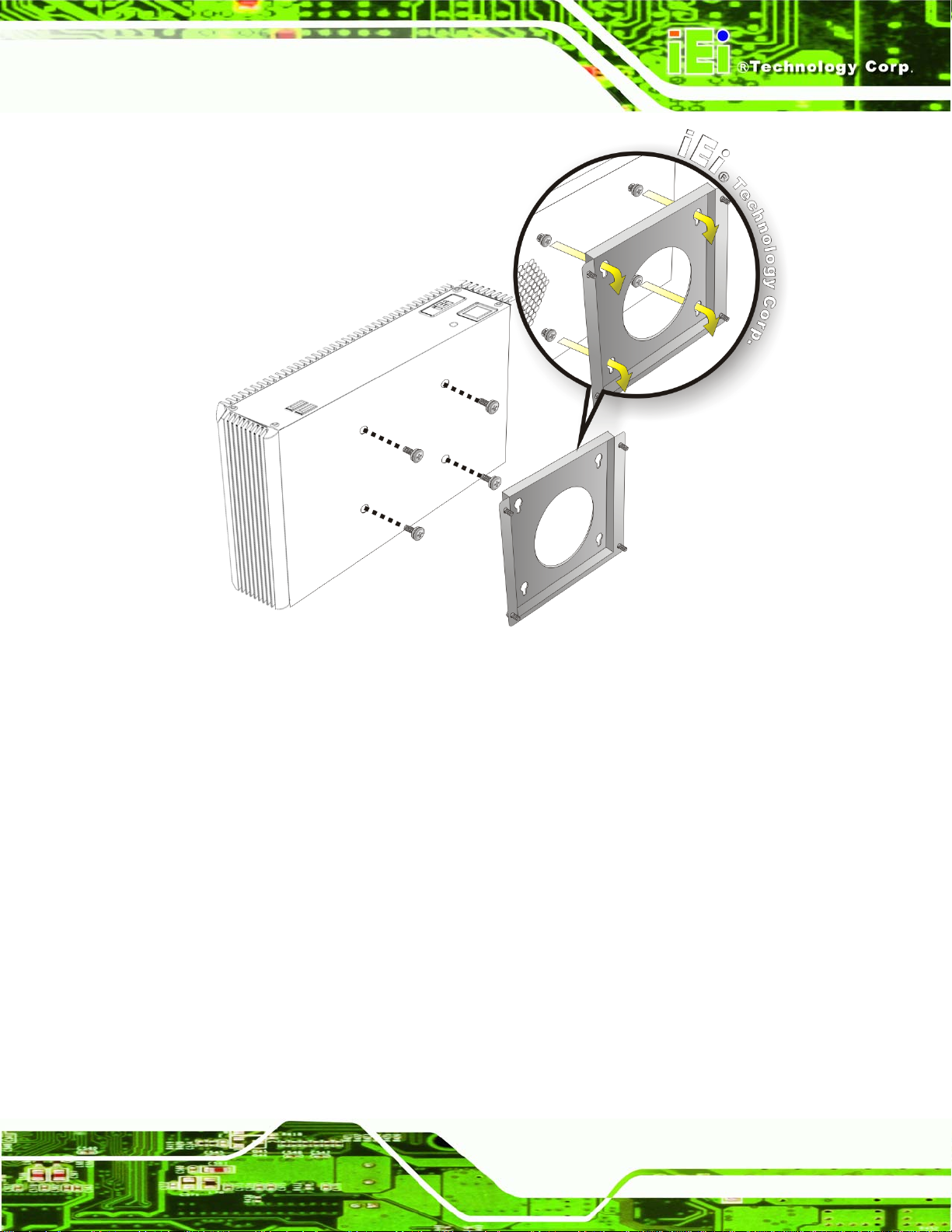
4.2.7 Mounting the System with Wall Mount Kit
To mount the embedded system onto a wall using the VESA MIS-D 100 wall mount kit,
please follow the steps below.
Step 1: Select the location on the wall for the wall-mounting bracket.
Step 2: Carefully mark the locations of the four bracket screw holes on the wall.
Step 3: Drill four pilot holes at the marked locations on the wall for the bracket retention
screws.
Step 4: Align the wall-mounting bracket screw holes with the pilot holes.
Step 5: Secure the mounting-bracket to the wall by inserting the retention screws into
the four pilot holes and tightening them (
Figure 4-7).
Page 71
Page 72

ECW-281BB6 Embedded System
Figure 4-7: Wall-mounting Bracket
Step 6: Insert the four monitor mounting screws provided in the wall mounting kit into the
four screw holes on the bottom panel of the system and tighten until the screw
shank is secured against the bottom panel (
Step 1: Align the mounting screws on the ECW-281BB6 bottom panel with the mounting
holes on the bracket.
Step 2: Carefully insert the screws through the holes and gently pull the monitor
downwards until the ECW-281BB6 rests securely in the slotted holes (
). Ensure that all four of the mounting screws fit snuggly into their respective
4-8
slotted holes.
Figure 4-8).
Figure
NOTE:
In the diagram below the bracket is already installed on the wall.
Page 72
Page 73
ECW-281BB6 Embedded System
Figure 4-8: Mount the Embedded System
4.2.8 DIN Mounting
To mount the ECW-281BB6 embedded system onto a DIN rail, please follow the steps
below.
Step 3: Attach the DIN rail mounting bracket to the bottom panel of the embedded
system. Secure the bracket to the embedded system with the supplied retention
screws (
Figure 4-9).
Page 73
Page 74

ECW-281BB6 Embedded System
Figure 4-9: DIN Rail Mounting Bracket
Step 4: Make sure the inserted screw in the center of the bracket is at the lowest
position of the elongated hole (
Figure 4-10).
Figure 4-10: Screw Locations
Step 5: Place the DIN rail flush against the back of the mounting bracket making sure
the edges of the rail are between the upper and lower clamps (
Figure 4-11).
Page 74
Page 75
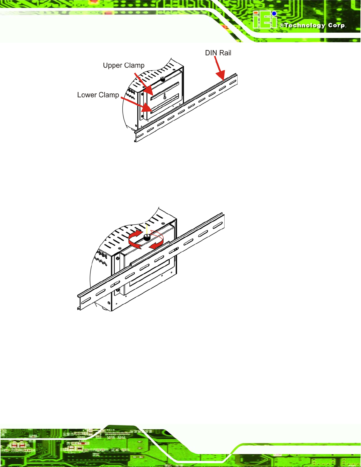
ECW-281BB6 Embedded System
Figure 4-11: Mounting the DIN RAIL
Step 6: Secure the DIN rail to the mounting bracket by turning the top screw clockwise.
This draws the lower clamp up and secures the embedded system to the DIN
Figure 4-12).Step 0:
rail (
Figure 4-12: Secure the Assembly to the DIN Rail
4.2.9 Cable Connections
Once the system has been mounted on the wall, the following connectors can be
connected to the system.
VGA cable connector
Serial port connectors
RJ-45 connectors
Page 75
Page 76

USB devices can be connected to the system.
ECW-281BB6 Embedded System
The cable connection locations are shown in
4.3 Power-On Procedure
4.3.1 Installation Checklist
WARNING:
Make sure a power supply with the correct input voltage is being fed into
the system. Incorrect voltages applied to the system may cause damage to
the internal electronic components and may also cause injury to the user.
To power on the embedded system please make sure of the following:
The bottom surface panel is installed
All peripheral devices (VGA monitor, serial communications devices etc.) are
Figure 2-5.
connected
The power cables are plugged in
The system is securely mounted
4.3.2 Terminal Block Pinouts
The terminal block pinouts are shown in Figure 4-13.
Figure 4-13: Terminal Block Pinouts
Page 76
Page 77

ECW-281BB6 Embedded System
The chassis ground is connected to the ECW chassis internally. The cable ground is
connected to the ground pin on the input power connector of the power module.
4.3.3 Power-on Procedure
To power-on the ECW-281BB6 please follow the steps below:
Step 1: Push the power button.
Step 2: Once turned on, the power button should turns to blue. See
Step 0:
Figure 4-14.
Figure 4-14: Power Button
Page 77
Page 78

ECW-281BB6 Embedded System
THIS PAGE IS INTENTIONALLY LEFT BLANK
Page 78
Page 79

ECW-281BB6 Embedded System
Chapter
5
5 BIOS Settings
Page 79
Page 80

5.1 Introduction
A licensed copy of AMI BIOS is preprogrammed into the ROM BIOS. The BIOS setup
program allows users to modify the basic system configuration. This chapter describes
how to access the BIOS setup program and the configuration options that may be
changed.
5.1.1 Starting Setup
The AMI BIOS is activated when the computer is turned on. The setup program can be
activated in one of two ways.
ECW-281BB6 Embedded System
1. Press the D
2. Press the D
appears on the screen. 0.
If the message disappears before the D
again.
ELETE key as soon as the system is turned on or
ELETE key when the “Press Del to enter SETUP” message
ELETE key is pressed, restart the computer and try
5.1.2 Using Setup
Use the arrow keys to highlight items, press ENTER to select, use the PageUp and
PageDown keys to change entries, press F1 for help and press E
keys are shown in.
Key Function
Up arrow Move to previous item
Down arrow Move to next item
Left arrow Move to the item on the left hand side
SC to quit. Navigation
Page 80
Right arrow Move to the item on the right hand side
Esc key Main Menu – Quit and not save changes into CMOS
Status Page Setup Menu and Option Page Setup Menu --
Exit current page and return to Main Menu
“+” key Increase the numeric value or make changes
“-“ key Decrease the numeric value or make changes
Page 81

ECW-281BB6 Embedded System
F1 key General help, only for Status Page Setup Menu and Option
Page Setup Menu
F2 /F3 key Change color from total 16 colors. F2 to select color
forward.
F10 key Save all the CMOS changes, only for Main Menu
Table 5-1: BIOS Navigation Keys
5.1.3 Getting Help
When F1 is pressed a small help window describing the appropriate keys to use and the
possible selections for the highlighted item appears. To exit the Help Window press E
SC or
the F1 key again.
5.1.4 Unable to Reboot After Configuration Changes
If the computer cannot boot after changes to the system configuration is made, CMOS
defaults. Use the jumper described in Chapter Error! Reference source not found.,
Section
3.5.1.
5.1.5 BIOS Menu Bar
The menu bar on top of the BIOS screen has the following main items:
Main Changes the basic system configuration.
Advanced Changes the advanced system settings.
PCIPnP Changes the advanced PCI/PnP Settings
Boot Changes the system boot configuration.
Security Sets User and Supervisor Passwords.
Chipset Changes the chipset settings.
Power Changes power management settings.
Exit Selects exit options and loads default settings
The following sections completely describe the configuration options found in the menu
items at the top of the BIOS screen and listed above.
Page 81
Page 82

5.2 Main
The Main BIOS menu (BIOS Menu 1) appears when the BIOS Setup program is entered.
The Main menu gives an overview of the basic system information.
ECW-281BB6 Embedded System
BIOS Menu 1: Main
System Overview
The System Overvie w lists a brief summary of different system components. The fields in
System Overview cannot be changed. The items shown in the system overview include:
AMI BIOS: Displays auto-detected BIOS information
Processor: Displays auto-detected CPU specifications
Page 82
o Version: Current BIOS version
o Build Date: Date the current BIOS version was made
o ID: Installed BIOS ID
o Type: Names the currently installed processor
o Speed: Lists the processor speed
Page 83

ECW-281BB6 Embedded System
o Count: The number of CPUs on the motherboard
System Memory: Displays the auto-detected system memory.
o Size: Lists memory size
The System Overview field also has two user configurable fields:
System Time [xx:xx:xx]
Use the System Time option to set the system time. Manually enter the hours, minutes
and seconds.
System Date [xx/xx/xx]
Use the System Date option to set the system date. Manually enter the day, month and
year.
5.3 Advanced
Use the Advanced menu (BIOS Menu 2) to configure the CPU and peripheral devices
through the following sub-menus:
WARNING:
Setting the wrong values in the sections below may cause the system to
malfunction. Make sure that the settings made are compatible with the
hardware.
CPU Configuration (see Section 5.3.1)
IDE Configuration (see Section 5.3.2)
SuperIO Configuration (see Section 5.3.3)
Hardware Health Configuration (see Section 0)
MPS Configuration (see Section 5.3.5)
Trusted Computing (see Section 0)
USB Configuration (see Section 5.3.7)
Page 83
Page 84

ECW-281BB6 Embedded System
BIOS Menu 2: Advanced
5.3.1 CPU Configuration
Use the CPU Configuration menu (BIOS Menu 3) to view detailed CPU specifications and
configure the CPU.
Page 84
Page 85

ECW-281BB6 Embedded System
BIOS Menu 3: CPU Configuration
The CPU Configuration menu (
Manufacturer: Lists the name of the CPU manufacturer
Brand String: Lists the brand name of the CPU being used
Frequency: Lists the CPU processing speed
FSB Speed: Lists the FSB speed
Cache L1: Lists the CPU L1 cache size
Cache L2: Lists the CPU L2 cache size
BIOS Menu 3) lists the following CPU details:
The following CPU Configuration menu item can be configured.
Execute Disable Bit
Intel® SpeedStep™ tech
Page 85
Page 86

Execute Bit Disable [Enabled]
Use the Execute Bit Disable BIOS function to protect the system from buffer overflow
attacks.
ECW-281BB6 Embedded System
Disabled
Enabled D
Code can be executed in any memory area.
EFAULT
Code execution in data-only memory pages is
prohibited.
5.3.2 IDE Configuration
Use the IDE Configuration menu (BIOS Menu 4) to change and/or set the configuration
of the IDE devices installed in the system.
BIOS Menu 4: IDE Configuration
OnBoard PCI IDE Controller [Both]
Page 86
Page 87

ECW-281BB6 Embedded System
Use the OnBoard PCI IDE Controller BIOS option to specify the IDE channels used by
the onboard PCI IDE controller. The following configuration options are available.
Disabled
Primary
Secondary
Both DEFAULT
Prevents the system from using the onboard IDE
controller
Only allows the system to detect the Primary IDE
channel, including both the Primary Master and the
Primary Slave
Only allows the system to detect the Secondary IDE
channel, including both the Secondary Master and
Secondary Slave
Allows the system to detect both the Primary and
Secondary IDE channels including the Primary Master,
Primary Slave, Secondary Master and Secondary
Slave.
Onboard PCI IDE Operate Mode [Legacy Mode]
Use the Onboard PCI IDE Operate Mode BIOS option to set the running mode for the
PCI IDE.
Legacy Mode DEFAULT
Native Mode
Hard Disk Write Protect [Disabled]
The Hard Disk Write Protect BIOS option protects the hard disks from being overwritten.
This menu item is only effective if the device is accessed through the BIOS.
Disabled DEFAULT
The PCI IDE mode is the native mode
The PCI IDE mode is the same as the IDE mode
Allows hard disks to be overwritten
Page 87
Page 88

ECW-281BB6 Embedded System
Enabled
Prevents hard disks from being overwritten
IDE Detect Time Out (Sec) [35]
The IDE Detect Time Out (Sec) BIOS option specifies the maximum time (in seconds) the
AMI BIOS will search for IDE devices. This allows fine-tunes the settings to allow for faster
boot times. The following configuration options are available.
0 seconds
5 seconds
10 seconds
15 seconds
20 seconds
25 seconds
30 seconds
35 seconds (Default)
The best setting to use if the onboard IDE controllers are set to a specific IDE disk drive in
the AMI BIOS is “0 seconds” and a large majority of ultra ATA hard disk drives can be
detected well within “35 seconds” (the default setting).
ATA (PI) 80Pin Cable Detection [Host & Device]
When an Ultra ATA/66, an Ultra ATA/100 or an Ultra ATA/133 IDE hard disk drive is used,
an 80-conductor ATA cable must be used. The 80-conductor ATA cable is plug compatible
with the standard 40-conductor ATA cable. The system must detect the presence of
correct cable so that the AMIBIOS can instruct the drive to run at the correct speed for the
cable type detected.
The ATA (PI) 80Pin Cable Detection BIOS option determines how the IDE cable will be
detected.
Host & Device DEFAULT
Both the motherboard onboard IDE controller and
IDE disk drive are used to detect the type of IDE
Page 88
Page 89

ECW-281BB6 Embedded System
cable used.
Host
Device
IDE Master and IDE Slave
When entering setup, BIOS auto detects the presence of IDE devices. BIOS displays the
status of the auto detected IDE devices. The following IDE devices are detected and are
shown in the IDE Configuration menu:
Primary IDE Master
Primary IDE Slave
Secondary IDE Master
Secondary IDE Slave
The motherboard onboard IDE controller detects
the type of IDE cable used.
The IDE disk drive to detects the type of IDE cable
used.
The IDE Configuration menu (
IDE devices installed in the system. If an IDE device is detected, and one of the above
listed four BIOS configuration options are selected, the IDE configuration options shown in
Section
5.3.2.1 appear.
BIOS Menu 4) allows changes to the configurations for the
5.3.2.1 IDE Master, IDE Slave
Use the IDE Master and IDE Slave configuration menu to view both primary and
secondary IDE device details and configure the IDE devices connected to the system.
Page 89
Page 90

ECW-281BB6 Embedded System
BIOS Menu 5: IDE Master and IDE Slave Configuration
Auto-Detected Drive Parameters
The “grayed-out” items in the left frame are IDE disk drive parameters automatically
detected from the firmware of the selected IDE disk drive. The drive parameters are listed
as follows:
Type: Lists the device type (e.g. hard disk, CD-ROM etc.)
LBA Mode: Indicates whether the LBA (Logical Block Addressing) is a
method of addressing data on a disk drive is supported or not.
Block Mode: Block mode boosts IDE drive performance by increasing the
amount of data transferred. Only 512 bytes of data can be transferred per
interrupt if block mode is not used. Block mode allows transfers of up to 64 KB
per interrupt.
PIO Mode: Indicates the PIO mode of the installed device.
DMA Mode: Indicates the highest Asynchronous DMA Mode that is
Page 90
supported.
Page 91

ECW-281BB6 Embedded System
S.M.A.R.T.: Indicates whether or not the Self-Monitoring Analysis and
Reporting Technology protocol is supported.
Type [Auto]
Use the Type BIOS option select the type of device the AMIBIOS attempts to boot from
after the Power-On Self-Test (POST) is complete.
Not Installed
Auto DEFAULT
CD/DVD
ARMD
BIOS is prevented from searching for an IDE disk
drive on the specified channel.
The BIOS auto detects the IDE disk drive type
attached to the specified channel. This setting should
be used if an IDE hard disk drive is attached to the
specified channel.
The CD/DVD option specifies that an IDE CD-ROM
drive is attached to the specified IDE channel. The
BIOS does not attempt to search for other types of
IDE disk drives on the specified channel.
This option specifies an ATAPI Removable Media
Device. These include, but are not limited to:
LBA/Large Mode [Auto]
Use the LBA/Large Mode option to disable or enable BIOS to auto detects LBA (Logical
Block Addressing). LBA is a method of addressing data on a disk drive. In LBA mode, the
maximum drive capacity is 137 GB.
Disabled
ZIP
LS-120
BIOS is prevented from using the LBA mode control on
Page 91
Page 92

the specified channel.
ECW-281BB6 Embedded System
Auto DEFAULT
Block (Multi Sector Transfer) [Auto]
Use the Block (Multi Sector Transfer) to disable or enable BIOS to auto detect if the
device supports multi-sector transfers.
Disabled
Auto DEFAULT
BIOS is prevented from using Multi-Sector Transfer on the
BIOS auto detects the LBA mode control on the specified
channel.
specified channel. The data to and from the device occurs
one sector at a time.
BIOS auto detects Multi-Sector Transfer support on the
drive on the specified channel. If supported the data
transfer to and from the device occurs multiple sectors at
a time.
PIO Mode [Auto]
Use the PIO Mode option to select the IDE PIO (Programmable I/O) mode program timing
cycles between the IDE drive and the programmable IDE controller. As the PIO mode
increases, the cycle time decreases.
Auto DEFAULT
0
1
2
3
PIO mode 0 selected with a maximum transfer rate of 3.3MBps
PIO mode 1 selected with a maximum transfer rate of 5.2MBps
PIO mode 2 selected with a maximum transfer rate of 8.3MBps
PIO mode 3 selected with a maximum transfer rate of 11.1MBps
BIOS auto detects the PIO mode. Use this value if the IDE disk
drive support cannot be determined.
Page 92
Page 93

ECW-281BB6 Embedded System
4
DMA Mode [Auto]
Use the DMA Mode BIOS selection to adjust the DMA mode options.
Auto DEFAULT
S.M.A.R.T [Auto]
Use the S.M.A.R.T option to auto-detect, disable or enable Self-Monitoring Analysis and
Reporting Technology (SMART) on the drive on the specified channel. S.M.A.R.T predicts
PIO mode 4 selected with a maximum transfer rate of 16.6MBps
(This setting generally works with all hard disk drives
manufactured after 1999. For other disk drives, such as IDE
CD-ROM drives, check the specifications of the drive.)
BIOS auto detects the DMA mode. Use this value if the IDE
disk drive support cannot be determined.
impending drive failures. The S.M.A.R.T BIOS option enables or disables this function.
Auto DEFAULT
Disabled
Enabled
32Bit Data Transfer [Disabled]
Use the 32Bit Data Transfer BIOS option to enables or disable 32-bit data transfers.
Disabled DEFAULT
Enabled
Prevents BIOS from using the HDD SMART feature.
Allows BIOS to use the HDD SMART feature
BIOS auto detects HDD SMART support.
Prevents the BIOS from using 32-bit data transfers.
Allows BIOS to use 32-bit data transfers on supported
hard disk drives.
5.3.3 Super IO Configuration
Page 93
Page 94

Use the Super IO Configuration menu (BIOS Menu 6) to set or change the
configurations for the FDD controllers, parallel ports and serial ports.
ECW-281BB6 Embedded System
BIOS Menu 6: Super IO Configuration
Serial Port1 Address [3F8/IRQ4]
Use the Serial Port1 Address option to select the Serial Port 1 base address.
Disabled
3F8/IRQ4 DEFAULT
3E8/IRQ4
2E8/IRQ3
No base address is assigned to Serial Port 1
Serial Port 1 I/O port address is 3F8 and the interrupt
address is IRQ4
Serial Port 1 I/O port address is 3E8 and the interrupt
address is IRQ4
Serial Port 1 I/O port address is 2E8 and the interrupt
address is IRQ3
Page 94
Page 95

ECW-281BB6 Embedded System
Serial Port1 Mode [Normal]
Use the Serial Port1 Mode option to select the transmitting and receiving mode for the
first serial port.
Normal
IrDA
ASK IR
Serial Port2 Address [2F8/IRQ3]
Use the Serial Port2 Address option to select the Serial Port 2 base address.
Disabled
2F8/IRQ3 DEFAULT
3E8/IRQ4
2E8/IRQ3
(Default) Serial Port 1 mode is normal
Serial Port 1 mode is IrDA
Serial Port 1 mode is ASK IR
No base address is assigned to Serial Port 2
Serial Port 2 I/O port address is 3F8 and the interrupt
address is IRQ3
Serial Port 2 I/O port address is 3E8 and the interrupt
address is IRQ4
Serial Port 2 I/O port address is 2E8 and the interrupt
address is IRQ3
Serial Port2 Mode [Normal]
Use the Serial Port2 Mode option to select the Serial Port2 operational mode.
Normal DEFAULT
IrDA
ASK IR
Restore on AC Power Loss [Po wer On]
Serial Port 2 mode is IrDA
Serial Port 2 mode is ASK IR
Serial Port 2 mode is normal
Page 95
Page 96

The Restore on AC Power Loss BIOS option specifies what state the system returns to if
there is a sudden loss of power to the system.
ECW-281BB6 Embedded System
Power Off
Power On DEFAULT
Last State
Serial Port3 Address [3E8]
Use the Serial Port3 Address option to select the base addresses for serial port 3
Disabled
3E8 DEFAULT
2F8
3E8
2E8
The system remains turned off
The system turns on
The system returns to its previous state. If it was on, it
turns itself on. If it was off, it remains off.
No base address is assigned to serial port 3
Serial port 3 I/O port address is 3E8
Serial port 3 I/O port address is 2F8
Serial port 3 I/O port address is 3E8
Serial port 3 I/O port address is 2E8
2F0
2E0
Serial Port3 IRQ [11]
Use the Serial Port3 IRQ option to select the interrupt address for serial port 3.
4
9
10
11 DEFAULT
Page 96
Serial port 3 I/O port address is 2F0
Serial port 3 I/O port address is 2E0
Serial port 3 IRQ address is 4
Serial port 3 IRQ address is 9
Serial port 3 IRQ address is 10
Serial port 3 IRQ address is 11
Page 97

ECW-281BB6 Embedded System
Serial Port4 Address [2E8]
Use the Serial Port4 IRQ option to select the interrupt address for serial port 4.
Disabled
3F8
2F8
3E8
2E8 DEFAULT
2F0
2E0
Serial Port4 IRQ [10]
Use the Serial Port4 IRQ option to select the interrupt address for serial port 4.
3
No base address is assigned to serial port 3
Serial port 4 I/O port address is 3F8
Serial port 4 I/O port address is 2F8
Serial port 4 I/O port address is 3E8
Serial port 4 I/O port address is 2E8
Serial port 4 I/O port address is 2F0
Serial port 4 I/O port address is 2E0
Serial port 4 IRQ address is 3
9
10 DEFAULT
11
Serial Port5 Address [2F0]
Use the Serial Port5 IRQ option to select the interrupt address for serial port 5.
Disabled
3E8
2E8
2F0 DEFAULT
Serial port 4 IRQ address is 9
Serial port 4 IRQ address is 10
Serial port 4 IRQ address is 11
No base address is assigned to serial port 3
Serial port 5 I/O port address is 3E8
Serial port 5 I/O port address is 2E8
Serial port 5 I/O port address is 2F0
Page 97
Page 98

ECW-281BB6 Embedded System
2E0
2D8
2D0
Serial Port5 IRQ [11]
Use the Serial Port5 IRQ option to select the interrupt address for serial port 5.
3
9
10
11 DEFAULT
Serial Port6 Address [2E0]
Serial port 5 I/O port address is 2D8
Serial port 5 I/O port address is 2D0
Serial port 4 IRQ address is 3
Serial port 4 IRQ address is 9
Serial port 5 I/O port address is 2E0
Serial port 4 IRQ address is 10
Serial port 4 IRQ address is 11
Use the Serial Port6 IRQ option to select the interrupt address for serial port6.
Disabled
3E8
2E8
2F0
2E0 DEFAULT
2D8
2D0
Serial Port6 IRQ [10]
Use the Serial Port6 IRQ option to select the interrupt address for serial port 6.
No base address is assigned to serial port 3
Serial port 6 I/O port address is 3E8
Serial port 6 I/O port address is 2E8
Serial port 6 I/O port address is 2F0
Serial port 6 I/O port address is 2E0
Serial port 6 I/O port address is 2D8
Serial port 6 I/O port address is 2D0
Page 98
Page 99

ECW-281BB6 Embedded System
3
9
10 DEFAULT
11
Serial port 6 IRQ address is 3
Serial port 6 IRQ address is 9
Serial port 6 IRQ address is 10
Serial port 6 IRQ address is 11
5.3.4 Hardware Health Configuration
The Hardware Health Configuration menu (BIOS Menu 7) shows the operating
temperature, fan speeds and system voltages.
BIOS Menu 7: Hardware Health Configuration
The following system parameters and values are shown. The system parameters that are
monitored are:
Page 99
Page 100

System Temperatures: The following system temperatures are monitored
o Temperature Sensor #1
o Temperature Sensor #2
Voltages: The following system voltages are monitored
o CPU Core
o VCC
o +3.3V
o +5.0V
o +1.5V
o VBAT
5.3.5 MPS Configuration
Use the MPS Configuration menu (BIOS Menu 8) to select `he multi-processor table.
ECW-281BB6 Embedded System
BIOS Menu 8: MPS Configuration
MPS Revision [1.1]
Page 100
 Loading...