

Page 1
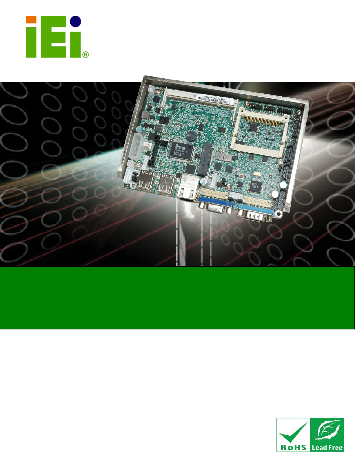
WAFER-945GSELVDS2
IEI Technology Corp.
MODEL:
WAFER-945GSELVDS2
3.5" SBC with 1.6 GHz Intel® ATOM™ N270
VGA, Dual LVDS, Gigabit Ethernet, CompactFlash®
Audio and SATA, RoHS Compliant
User Manual
Rev. 1.01 – 12 August, 2011
Page i
Page 2
Date Version Changes
WAFER-945GSELVDS2
Revision
12 August, 2011 1.01
24 September, 2009 1.00 Initial release
Modified SATA connector description
Page ii
Page 3
WAFER-945GSELVDS2
COPYRIGHT NOTICE
The information in this document is subject to change without prior notice in order to
improve reliability, design and function and does not represent a commitment on the part
of the manufacturer.
In no event will the manufacturer be liable for direct, indirect, special, incidental, or
consequential damages arising out of the use or inability to use the product or
documentation, even if advised of the possibility of such damages.
This document contains proprietary information protected by copyright. All rights are
Copyright
reserved. No part of this manual may be reproduced by any mechanical, electronic, or
other means in any form without prior written permission of the manufacturer.
TRADEMARKS
All registered trademarks and product names mentioned herein are used for identification
purposes only and may be trademarks and/or registered trademarks of their respective
owners.
Page iii
Page 4
WAFER-945GSELVDS2
Table of Contents
1 INTRODUCTION.......................................................................................................... 1
1.1 INTRODUCTION........................................................................................................... 2
1.2 OVERVIEW PHOTO...................................................................................................... 2
1.3 TECHNICAL SPECIFICATIONS ...................................................................................... 3
1.4 DIMENSIONS............................................................................................................... 5
1.5 DATA FLOW................................................................................................................ 7
2 UNPACKING................................................................................................................. 8
2.1 ANTI-STATIC PRECAUTIONS........................................................................................ 9
2.2 UNPACKING................................................................................................................ 9
2.2.1 Unpacking Precautions...................................................................................... 9
2.3 UNPACKING CHECKLIST........................................................................................... 10
2.3.1 Package Contents............................................................................................. 10
2.3.2 Optional Items...................................................................................................11
3 CONNECTORS ........................................................................................................... 12
3.1 PERIPHERAL INTERFACE CONNECTORS..................................................................... 13
3.2 PERIPHERAL INTERFACE CONNECTORS..................................................................... 13
3.2.1 Internal Peripheral Connectors....................................................................... 13
3.2.2 External Interface Panel Connectors............................................................... 14
3.3 INTERNAL PERIPHERAL CONNECTORS...................................................................... 15
3.3.1 ATX Power Connector ..................................................................................... 15
3.3.2 ATX Power Control Connector........................................................................ 15
3.3.3 Audio Connector .............................................................................................. 16
3.3.4 Battery Connector............................................................................................ 17
3.3.5 CompactFlash® Slot........................................................................................ 18
3.3.6 Digital I/O Connector...................................................................................... 20
3.3.7 CPU Fan Connector........................................................................................ 21
3.3.8 Keyboard/Mouse Connector............................................................................ 22
3.3.9 LED Connector................................................................................................ 23
3.3.10 LVDS1 LCD Connector ................................................................................. 24
Page iv
Page 5
WAFER-945GSELVDS2
3.3.11 LVDS1 Inverter Connector............................................................................. 26
3.3.12 LVDS2 LCD Connector ................................................................................. 26
3.3.13 LVDS2 Inverter Connector............................................................................ 28
3.3.14 PCIe Mini Card Slot ...................................................................................... 29
3.3.15 Power Button Connector................................................................................ 30
3.3.16 Reset Button Connector ................................................................................. 31
3.3.17 SATA Drive Connectors ................................................................................. 32
3.3.18 Serial Port Connector.................................................................................... 33
3.3.19 Serial Port Connector (RS-232/422/485) ...................................................... 34
3.3.20 USB Connector .............................................................................................. 35
3.4 EXTERNAL PERIPHERAL INTERFACE CONNECTOR PANEL ......................................... 36
3.4.1 LAN Connectors............................................................................................... 37
3.4.2 Serial Port Connector...................................................................................... 38
3.4.3 USB Connectors............................................................................................... 38
3.4.4 VGA Connector................................................................................................ 39
4 INSTALLATION ......................................................................................................... 40
4.1 ANTI-STATIC PRECAUTIONS...................................................................................... 41
4.2 INSTALLATION CONSIDERATIONS.............................................................................. 42
4.2.1 Installation Notices.......................................................................................... 42
4.2.2 Installation Checklist....................................................................................... 43
4.3 UNPACKING.............................................................................................................. 44
4.4 SO-DIMM INSTALLATION ....................................................................................... 44
4.5 CF CARD INSTALLATION .......................................................................................... 45
4.6 JUMPER SETTINGS .................................................................................................... 46
4.6.1 AT Power Select Jumper Settings..................................................................... 47
4.6.2 Audio Power Source......................................................................................... 48
4.6.3 CF Card Setup ................................................................................................. 49
4.6.4 Clear CMOS Jumper........................................................................................ 50
4.6.5 COM2 Mode Selection..................................................................................... 51
4.6.6 LVDS1 and LVDS2 Panel Resolution Jumper ................................................. 52
4.6.7 LVDS1 Voltage Selection.................................................................................. 53
4.6.8 LVDS2 Voltage Selection.................................................................................. 54
4.7 CHASSIS INSTALLATION............................................................................................ 55
4.7.1 Airflow.............................................................................................................. 55
Page v
Page 6

4.7.2 Motherboard Installation................................................................................. 56
4.8 INTERNAL PERIPHERAL DEVICE CONNECTIONS........................................................ 56
4.8.1 Audio Kit Installation....................................................................................... 56
4.8.2 SATA Drive Connection ................................................................................... 57
4.8.3 RS-232 Cable Connection................................................................................ 59
4.8.4 Keyboard/Mouse Y-cable Connector ............................................................... 60
4.8.5 USB Cable........................................................................................................ 62
4.9 EXTERNAL PERIPHERAL INTERFACE CONNECTION ................................................... 63
4.9.1 LAN Connection (Single Connector)............................................................... 63
4.9.2 Serial Device Connection ................................................................................ 64
4.9.3 USB Connection (Dual Connector)................................................................. 64
4.9.4 VGA Monitor Connection ................................................................................ 65
4.10 HEAT SINK ENCLOSURE.......................................................................................... 66
4.11 INSTALLING DRIVERS ............................................................................................. 67
WAFER-945GSELVDS2
5 BIOS.............................................................................................................................. 70
5.1 INTRODUCTION......................................................................................................... 71
5.1.1 Starting Setup................................................................................................... 71
5.1.2 Using Setup...................................................................................................... 71
5.1.3 Getting Help..................................................................................................... 72
5.1.4 Unable to Reboot After Configuration Changes.............................................. 72
5.1.5 BIOS Menu Bar................................................................................................ 72
5.2 MAIN........................................................................................................................ 73
5.3 ADVANCED ............................................................................................................... 74
5.3.1 CPU Configuration.......................................................................................... 75
5.3.2 IDE Configuration........................................................................................... 76
5.3.2.1 IDE Master, IDE Slave............................................................................. 77
5.3.3 Super IO Configuration ................................................................................... 82
5.3.4 Hardware Health Configuration...................................................................... 84
5.3.5 Power Configuration........................................................................................ 86
5.3.5.1 ACPI configuration ................................................................................... 87
5.3.5.2 APM Configuration................................................................................... 88
5.3.6 Remote Access Configuration.......................................................................... 90
5.3.7 USB Configuration........................................................................................... 93
5.3.7.1 USB Mass Storage Device Configuration................................................. 95
Page vi
Page 7

WAFER-945GSELVDS2
5.4 PCI/PNP................................................................................................................... 97
5.5 BOOT........................................................................................................................ 98
5.5.1 Boot Settings Configuration............................................................................. 99
5.5.2 Boot Device Priority...................................................................................... 101
5.5.3 Hard Disk Drives........................................................................................... 102
5.5.4 Removable Drives.......................................................................................... 102
5.5.5 CD/DVD Drives............................................................................................. 103
5.6 SECURITY............................................................................................................... 103
5.7 CHIPSET ................................................................................................................. 104
5.7.1 Northbridge Configuration............................................................................ 105
5.7.2 Southbridge Configuration ............................................................................ 108
5.8 EXIT....................................................................................................................... 109
A BIOS OPTIONS .........................................................................................................111
B TERMINOLOGY.......................................................................................................115
C DIGITAL I/O INTERFACE......................................................................................119
C.1 INTRODUCTION...................................................................................................... 120
C.2 DIO CONNECTOR PINOUTS.................................................................................... 120
C.3 ASSEMBLY LANGUAGE SAMPLES........................................................................... 121
C.3.1 Enable the DIO Input Function..................................................................... 121
C.3.2 Enable the DIO Output Function.................................................................. 121
D WA TCHDOG TIMER .............................................................................................. 122
E HAZARDOUS MATERIALS DISCLOSURE ....................................................... 125
E.1 HAZARDOUS MATERIALS DISCLOSURE TABLE FOR IPB PRODUCTS CER TIFIED AS
ROHS COMPLIANT UNDER 2002/95/EC WITHOUT MERCURY..................................... 126
Page vii
Page 8

WAFER-945GSELVDS2
List of Figures
Figure 1-1: WAFER-945GSELVDS2...............................................................................................2
Figure 1-2: WAFER-945GSELVDS2 Overview [Front View] .......................................................3
Figure 1-3: Main Dimensions (mm)...............................................................................................5
Figure 1-4: Bottom Dimensions (mm) ..........................................................................................6
Figure 1-5: External Interface Panel Dimensions (mm)..............................................................6
Figure 1-6: Data Flow Block Diagram...........................................................................................7
Figure 3-1: Connector and Jumper Locations [Front Side] .....................................................13
Figure 3-2: ATX Power Connector Location..............................................................................15
Figure 3-3: ATX Power Control Connector Location................................................................16
Figure 3-4: Audio Connector Pinouts.........................................................................................17
Figure 3-5: Battery Connector Location.....................................................................................18
Figure 3-6: CF Card Slot Location ..............................................................................................19
Figure 3-7: Digital I/O Connector Location ................................................................................21
Figure 3-8: CPU Fan Connector Location..................................................................................22
Figure 3-9: Keyboard/Mouse Connector Location....................................................................23
Figure 3-10: LED Connector Locations......................................................................................24
Figure 3-11: LVDS1 Location.......................................................................................................25
Figure 3-12: Backlight Connector Pinout Locations.................................................................26
Figure 3-13: LVDS2 Location.......................................................................................................27
Figure 3-14: Backlight Connector Pinout Locations.................................................................28
Figure 3-15: PCIe Mini Card Slot Location.................................................................................29
Figure 3-16: Power Button Connector Location........................................................................31
Figure 3-17: Reset Button Connector Locations.......................................................................32
Figure 3-18: SATA Drive Connector Locations.........................................................................33
Figure 3-19: Serial Port Connector Location.............................................................................34
Figure 3-20: RS-232/422/485 Serial Port Connector Location..................................................35
Figure 3-21: USB Connector Pinout Locations.........................................................................36
Figure 3-22: WAFER-945GSELVDS2 External Peripheral Interface Connector.....................36
Figure 3-23: RJ-45 Ethernet Connector......................................................................................37
Figure 3-24: Serial Port Pin Location..........................................................................................38
Page viii
Page 9

WAFER-945GSELVDS2
Figure 3-25: VGA Connector .......................................................................................................39
Figure 4-1: SO-DIMM Installation................................................................................................44
Figure 4-2: CF Card Installation..................................................................................................46
Figure 4-3: AT Power Select Jumper Location..........................................................................48
Figure 4-4: Audio Power Source.................................................................................................49
Figure 4-5: CF Card Setup Jumper Location.............................................................................50
Figure 4-6: Clear CMOS Jumper .................................................................................................51
Figure 4-7: COM 2 Function Select Jumper Location...............................................................52
Figure 4-8:LVDS Panel Resolution Jumper Pinout Locations.................................................53
Figure 4-9: LVDS1 Voltage Selection Jumper Pinout Locations.............................................54
Figure 4-10: LVDS Voltage Selection Jumper Pinout Locations.............................................55
Figure 4-11: Audio Kit Cable Connection ..................................................................................57
Figure 4-12: SATA Drive Cable Connection...............................................................................58
Figure 4-13: SATA Power Drive Connection..............................................................................59
Figure 4-14: Dual RS-232 Cable Installation..............................................................................60
Figure 4-15: Keyboard/mouse Y-cable Connection..................................................................61
Figure 4-16: Dual USB Cable Connection..................................................................................62
Figure 4-17: LAN Connection......................................................................................................63
Figure 4-18: Serial Device Connector.........................................................................................64
Figure 4-19: USB Connector........................................................................................................65
Figure 4-20: VGA Connector .......................................................................................................66
Figure 4-21: Heat Sink Retention Screws ..................................................................................67
Figure 4-22: Start Up Screen.......................................................................................................68
Figure 4-23: Select Operating System........................................................................................69
Figure 4-24: Drivers......................................................................................................................69
Page ix
Page 10

WAFER-945GSELVDS2
List of Tables
Table 1-1: Technical Specifications..............................................................................................4
Table 2-1: Packing List.................................................................................................................11
Table 2-2: Optional Items.............................................................................................................11
Table 3-1: Peripheral Interface Connectors...............................................................................14
Table 3-2: Rear Panel Connectors..............................................................................................14
Table 3-3: ATX Power Connector Pinouts .................................................................................15
Table 3-4: ATX Power Supply Enable Connector Pinouts .......................................................16
Table 3-5: Audio Connector Pinouts ..........................................................................................17
Table 3-6: Battery Connector Pinouts........................................................................................18
Table 3-7: CF Card Slot Pinouts..................................................................................................20
Table 3-8: Digital I/O Connector Location..................................................................................21
Table 3-9: CPU Fan Connector Pinouts......................................................................................22
Table 3-10: Keyboard/Mouse Connector Pinouts .....................................................................23
Table 3-11: LED Connector Pinouts ...........................................................................................24
Table 3-12: LVDS1 Pinouts..........................................................................................................25
Table 3-13: Backlight Connector Pinouts ..................................................................................26
Table 3-14: LVDS2 Pinouts..........................................................................................................28
Table 3-15: Backlight Connector Pinouts ..................................................................................29
Table 3-16: PCIe Mini Card Slot Pinouts ....................................................................................30
Table 3-17: Power Button Connector Pinouts...........................................................................31
Table 3-18: Reset Button Connector Pinouts............................................................................32
Table 3-19: SATA Drive Connector Pinouts...............................................................................33
Table 3-20: Serial Port Pinouts....................................................................................................34
Table 3-21: RS-232/RS-485 Serial Port Connector Pinouts......................................................35
Table 3-22: USB Port Connector Pinouts...................................................................................36
Table 3-23: LAN Pinouts ..............................................................................................................37
Table 3-24: RJ-45 Ethernet Connector LEDs.............................................................................37
Table 3-25: Serial Port Pinouts....................................................................................................38
Table 3-26: USB Port Pinouts......................................................................................................39
Table 3-27: VGA Connector Pinouts...........................................................................................39
Page x
Page 11

WAFER-945GSELVDS2
Table 4-1: Jumpers.......................................................................................................................47
Table 4-2: AT Power Select Jumper Settings ............................................................................48
Table 4-3: Audio Power Source...................................................................................................48
Table 4-4: CF Card Setup Jumper Settings ...............................................................................49
Table 4-5: Clear CMOS Jumper Settings....................................................................................51
Table 4-6: COM 2 Function Select Jumper Settings.................................................................51
Table 4-7: LVDS1 Panel Resolution............................................................................................52
Table 4-8: LVDS2 Panel Resolution............................................................................................52
Table 4-9: LVDS Voltage Selection Jumper Settings................................................................53
Table 4-10: LVDS2 Voltage Selection Jumper Settings............................................................54
Table 5-1: BIOS Navigation Keys................................................................................................72
Page xi
Page 12

WAFER-945GSELVDS2
BIOS Menus
BIOS Menu 1: Main.......................................................................................................................73
BIOS Menu 2: Advanced..............................................................................................................74
BIOS Menu 3: CPU Configuration...............................................................................................75
BIOS Menu 4: IDE Configuration.................................................................................................76
BIOS Menu 5: IDE Master and IDE Slave Configuration...........................................................77
BIOS Menu 6: Super IO Configuration........................................................................................82
BIOS Menu 7: Hardware Health Configuration..........................................................................84
BIOS Menu 8: Power Configuration............................................................................................86
BIOS Menu 9: ACPI Configuration..............................................................................................87
BIOS Menu 10: APM Configuration.............................................................................................88
BIOS Menu 11: Remote Access Configuration..........................................................................90
BIOS Menu 12: USB Configuration.............................................................................................93
BIOS Menu 13: USB Mass Storage Device Configuration........................................................95
BIOS Menu 14: PCI/PnP Configuration.......................................................................................97
BIOS Menu 15: Boot.....................................................................................................................98
BIOS Menu 16: Boot Settings Configuration.............................................................................99
BIOS Menu 17: Boot Device Priority Settings ........................................................................ 101
BIOS Menu 18: Hard Disk Drives ............................................................................................. 102
BIOS Menu 19: Removable Drives........................................................................................... 102
BIOS Menu 20: CD/DVD Drives ................................................................................................ 103
BIOS Menu 21: Security............................................................................................................ 103
BIOS Menu 22: Chipset............................................................................................................. 104
BIOS Menu 23:Northbridge Chipset Configuration................................................................ 105
BIOS Menu 24:Southbridge Chipset Configuration............................................................... 108
BIOS Menu 25:Exit..................................................................................................................... 109
WAFER-945GSELVDS2
Page xii
Page 13
WAFER-945GSELVDS2
Chapter
1
1 Introduction
Page 1
Page 14
1.1 Introduction
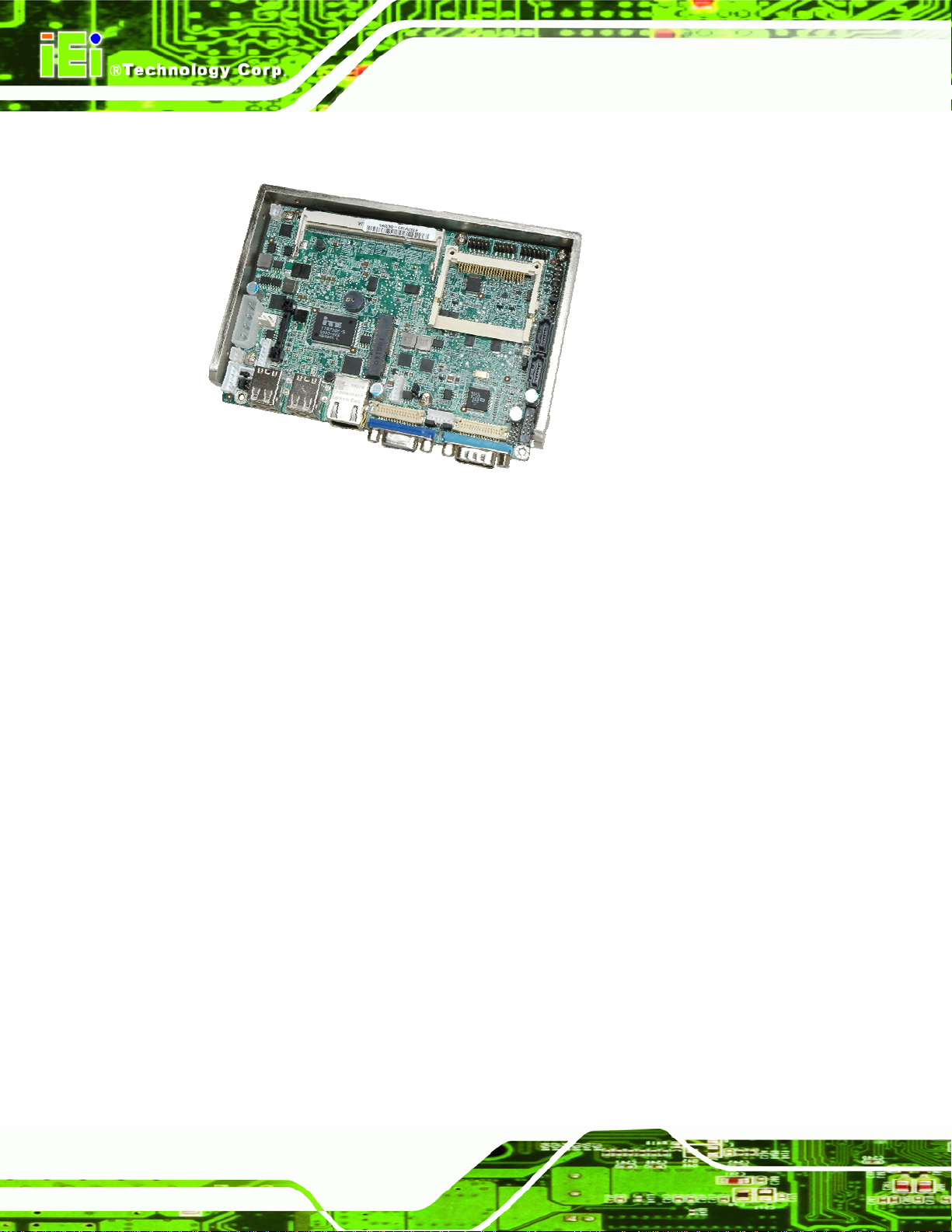
Figure 1-1: WAFER-945GSELVDS2
WAFER-945GSELVDS2
The WAFER-945GSELVDS2 is a 3.5" motherboard with a 1.6 GHz Intel® ATOM™ N270
processor with 512 KB L2 cache. Also supports one supports one 400 MHz or 533 MHz
DDR2 SO-DIMM up to 2.0 GB.
The WAFER-945GSELVDS2 has 18-bit and 24-bit dual-channel LVDS connectors, and a
single VGA video output.
External connectors include USB and Gigabit Ethernet connectors. Expansion options
include SATA slots, a PCIe Mini card slot, serial port connectors, CompactFlash® card
slot and audio connector.
1.2 Overview Photo
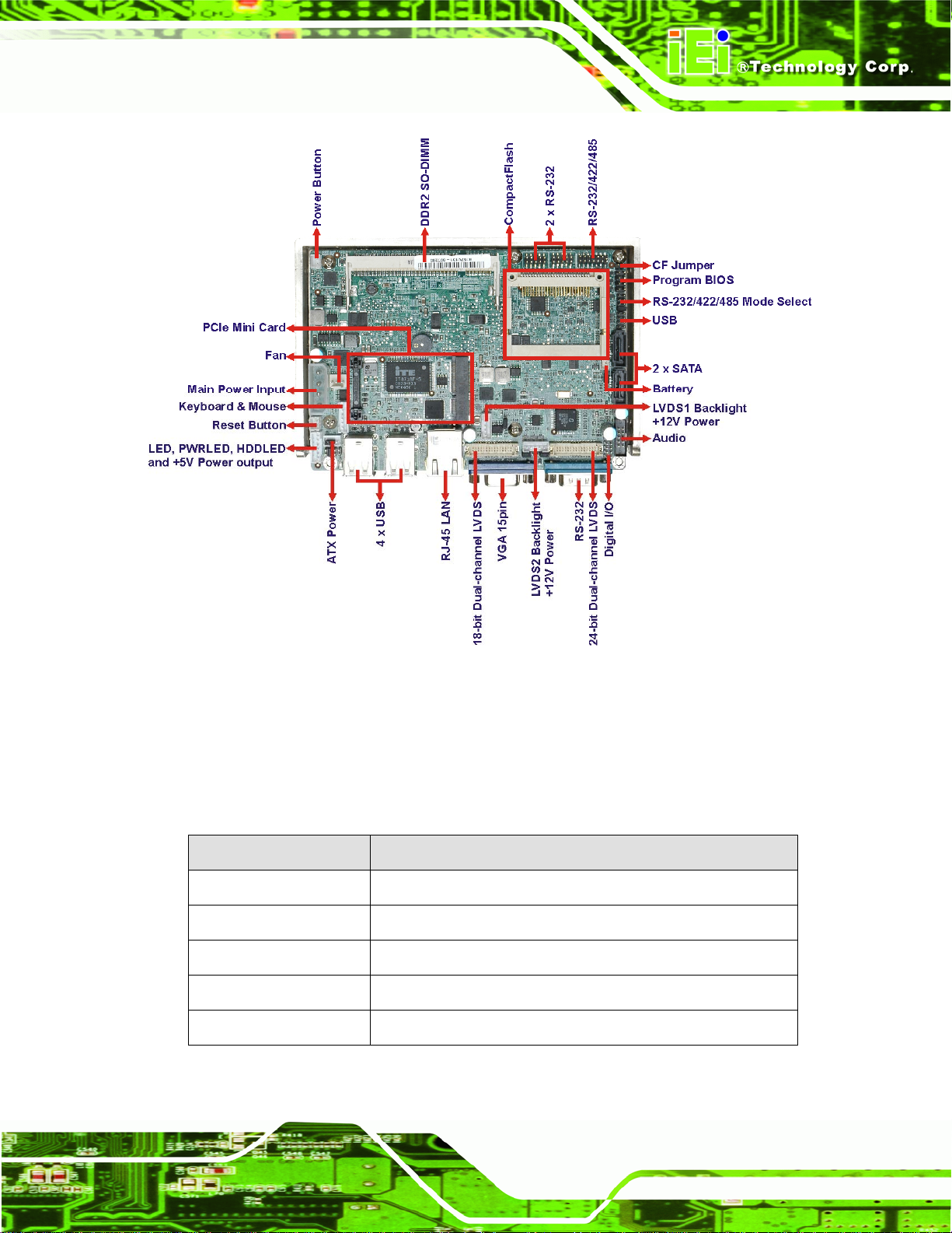
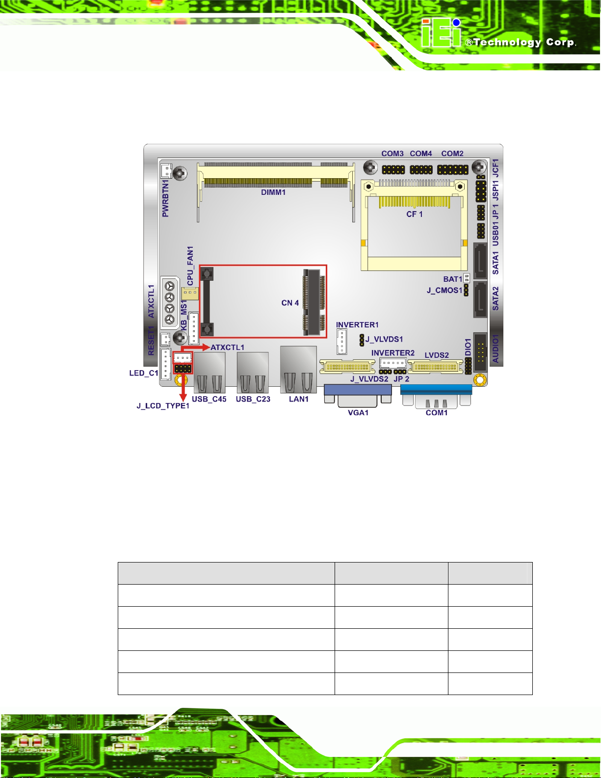
The WAFER-945GSELVDS2 has a wide variety of peripheral interface connectors. Figure
1-2 is a labeled photo of the peripheral interface connectors on the
WAFER-945GSELVDS2.
Page 2
Page 15
WAFER-945GSELVDS2
Figure 1-2: WAFER-945GSELVDS2 Overview [Front View]
1.3 Technical Specifications
WAFER-945GSELVDS2 technical specifications are listed in Table 1-1. See Chapter 2
for details.
Specification WAFER-945GSELVDS2
Form Factor
System CPU
Front Side Bus (FSB)
Northbridge
Southbridge
3.5"
1.6 GHz Intel® ATOM™ N270
533 MHz
Intel® 945GSE
Intel® ICH7M
Page 3
Page 16
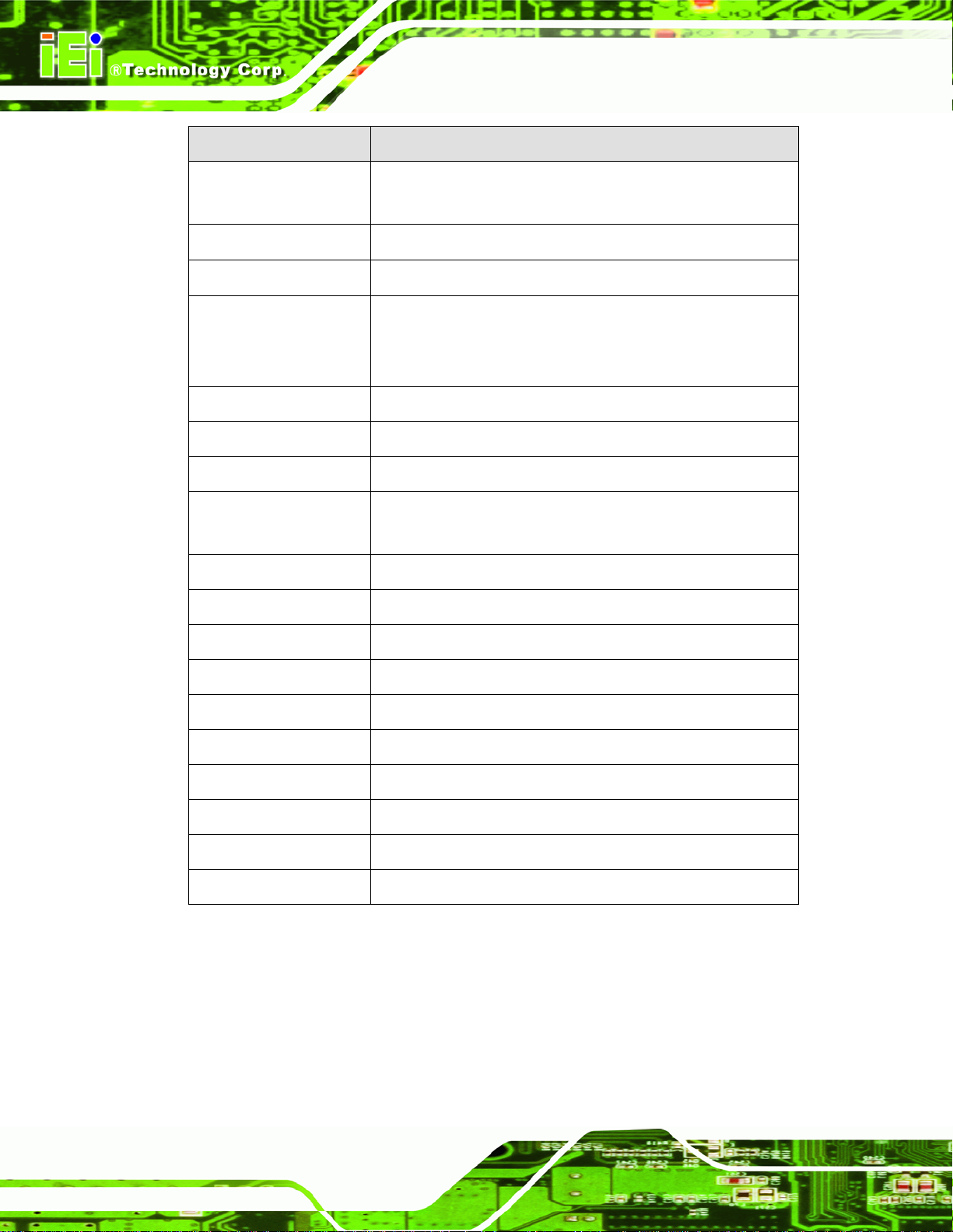
Specification WAFER-945GSELVDS2
WAFER-945GSELVDS2
Memory
CompactFlash®
Super I/O
Display
BIOS
Audio
LAN
COM
USB2.0
SATA
One 200-pin SO-DIMM socket supports one 400 MHz or
533 MHz 2.0 GB (max.) DDR2 SDRAM SO-DIMM
One CompactFlash® Type II socket
ITE IT8718
18-bit dual-channel LVDS
24-bit dual-channel LVDS
VGA
AMI
Realtek ALC655 AC'97 audio chip
1 x Realtek 8111CP PCIe GbE chi ps
3 x RS-232 serial ports (one external, two internal)
1 x RS-232/422/485 serial port (internal)
6 x USB (four external, two internal)
Two 3.0 Gb/s SATA drives supported
Keyboard/mouse
Expansion
Digital I/O
Power Consumption
Temperature
Humidity (operating)
Dimensions (LxW)
Weight (GW/NW)
Table 1-1: Technical Specifications
One internal pin-header connector
One PCIe mini card
8-bit (4-bit input, 4-bit output)
2.49 A @ 5 V (1.6 GHz Intel ATOM N270 with 2 GB DDR2)
0ºC – 60ºC (32ºF - 140ºF)
5%~95% non-condensing
102 mm x 146 mm
700 g / 350 g
Page 4
Page 17
WAFER-945GSELVDS2
1.4 Dimensions
The dimensions of the board are shown below:
Figure 1-3: Main Dimensions (mm)
Page 5
Page 18
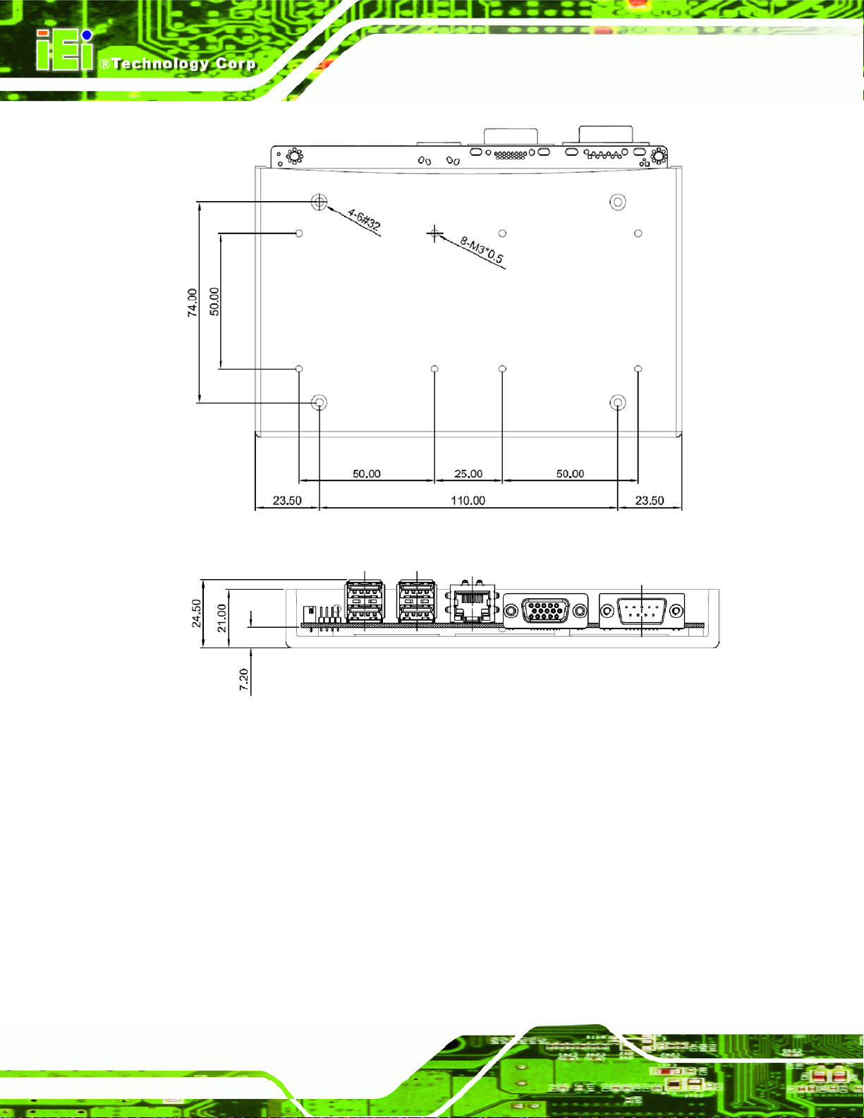
WAFER-945GSELVDS2
Figure 1-4: Bottom Dimensions (mm)
Figure 1-5: External Interface Panel Dimensions (mm)
Page 6
Page 19
WAFER-945GSELVDS2
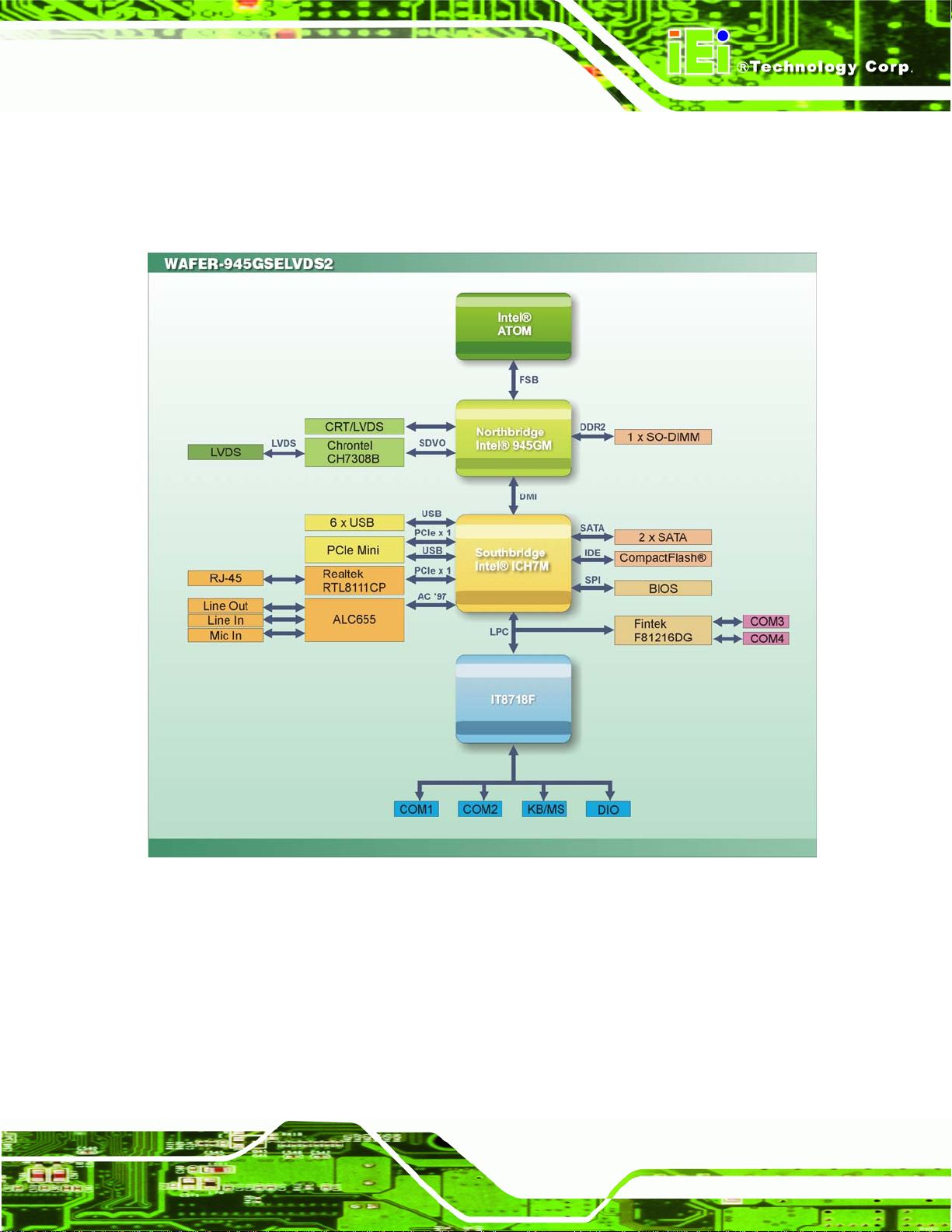
1.5 Data Flow
Figure 1-6 shows the data flow between the two on-board chipsets and other components
installed on the motherboard and described in the following sections of this chapter.
Figure 1-6: Data Flow Block Diagram
Page 7
Page 20
WAFER-945GSELVDS2
Chapter
2
2 Unpacking
Page 8
Page 21
WAFER-945GSELVDS2
2.1 Anti-static Precautions
WARNING!
Failure to take ESD precautions during the installation of the
WAFER-945GSELVDS2 may result in permanent damage to the
WAFER-945GSELVDS2 and severe injury to the user.
Electrostatic discharge (ESD) can cause serious damage to electronic components,
including the WAFER-945GSELVDS2. Dry climates are especially susceptible to ESD. It
is therefore critical that whenever the WAFER-945GSELVDS2, or any other electrical
component is handled, the following anti-static precautions are strictly adhered to.
Wear an anti-static wristband: - Wearing a simple anti-static wristband can
help to prevent ESD from damaging the board.
Self-grounding:- Before handling the board touch any grounded conducting
material. During the time the board is handled, frequently touch any
conducting materials that are connected to the ground.
Use an anti-static pad: When configuring the WAFE R-945GSELVDS2, place
it on an antic-static pad. This reduces the possibility of ESD damaging the
WAFER-945GSELVDS2.
Only handle the edges of the PCB:- When handling the PCB, hold the PCB
by the edges.
2.2 Unpacking
2.2.1 Unpacking Precautions
When the WAFER-945GSELVDS2 is unpacked, please do the following:
Follow the anti-static precautions outlined in Section
Make sure the packing box is facing upwards so the WAFER-945GSELVDS2
2.1.
does not fall out of the box.
Make sure all the components shown in Section
2.3 are present.
Page 9
Page 22
2.3 Unpacking Checklist
NOTE:
If any of the components listed in the checklist below are missing, do
not proceed with the installation. Contact the IEI reseller or vendor the
WAFER-945GSELVDS2 was purchased from or contact an IEI sales
WAFER-945GSELVDS2
representative directly by sending an email to
sales@iei.com.tw.
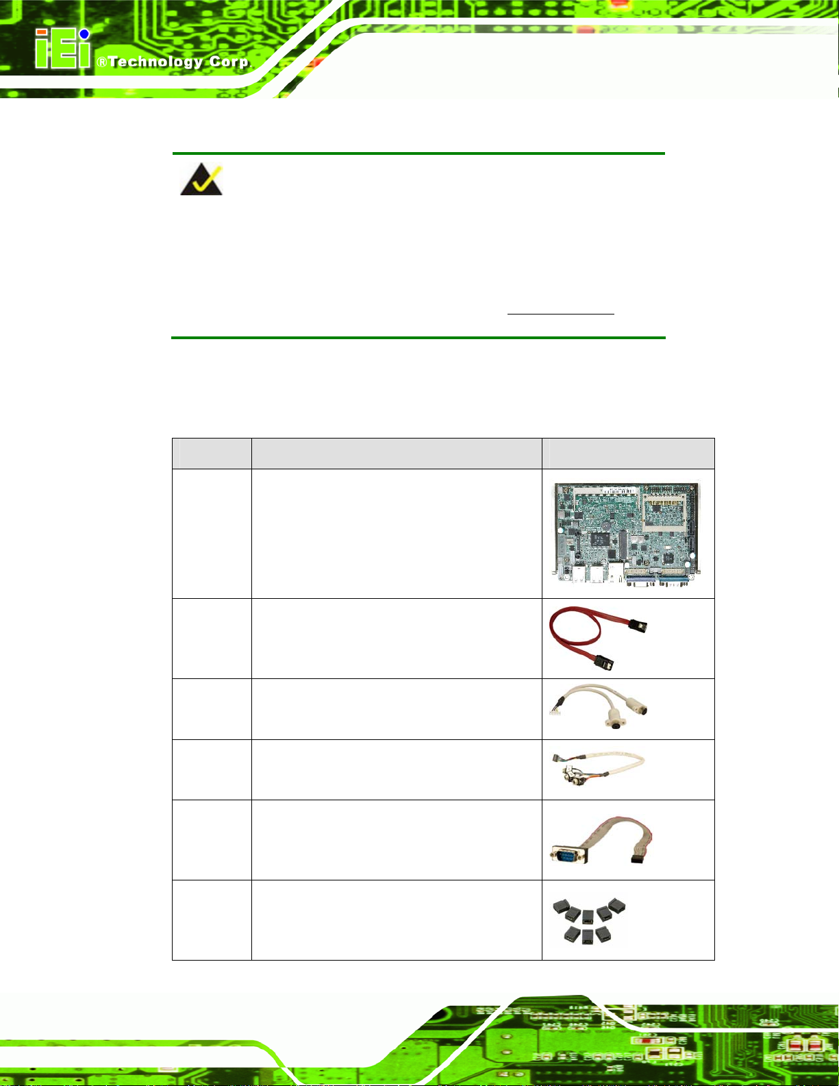
2.3.1 Package Contents
The WAFER-945GSELVDS2 is shipped with the following components:
Quantity Item and Part Number Image
1 WAFER-945GSELVDS2
2 SATA cable
(P/N: 32000-062800-RS)
1 KB/MS Cable
Page 10
(P/N: 32000-023800-RS)
1 Audio cable
(P/N: 32000-072100-RS)
1 Serial port cable
(P/N: 32200-000049-RS)
1 Mini jumper pack (2.0mm)
(P/N:33100-000033-RS)
Page 23
WAFER-945GSELVDS2
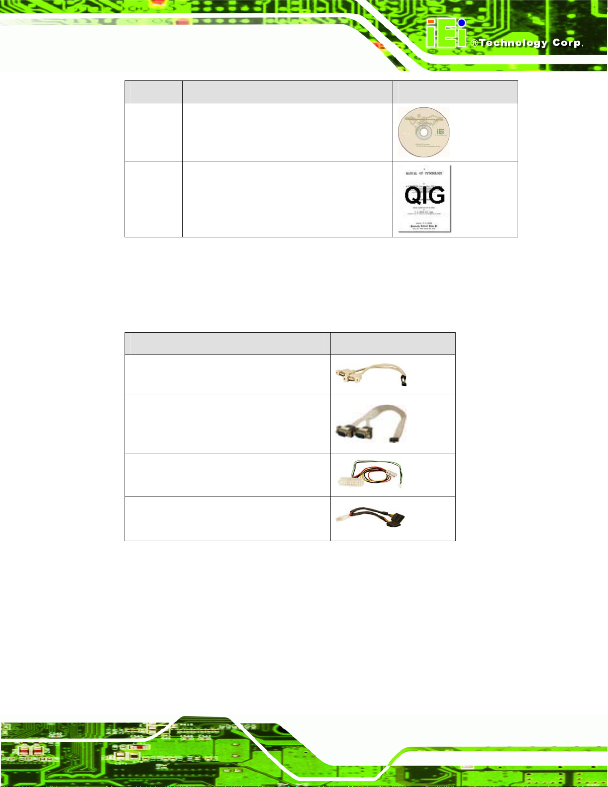
Quantity Item and Part Number Image
1 Utility CD
1 Quick Installation Guide
Table 2-1: Packing List
2.3.2 Optional Items
The WAFER-945GSELVDS2 is shipped with the following components:
Item and Part Number Image
Dual USB cable (wo bracket)
(P/N: 32000-070301-RS)
RS-232/422/485 cable
(P/N:32200-026500-RS)
ATX cable
(P/N: 32100-052100)
SATA power cable
(P/N: 32100-088600-RS)
Table 2-2: Optional Items
Page 11
Page 24

WAFER-945GSELVDS2
Chapter
3
3 Connectors
Page 12
Page 25
WAFER-945GSELVDS2
3.1 Peripheral Interface Connectors
The connectors on the WAFER-945GSELVDS2 are shown in the diagram below.
Figure 3-1: Connector and Jumper Locations [Front Side]
3.2 Peripheral Interface Connectors
Table 3-1 shows a list of the peripheral interface connectors on the
WAFER-945GSELVDS2. Detailed descriptions of these connectors can be found below.
3.2.1 Internal Peripheral Connectors
Connector Type Label
ATX enable connector 3-pin wafer ATXCTL1
ATX power connector 4-pin molex ATXPWR1
Audio connector 10-pin header AUDIO1
Battery connector 2-pin box header BT1
CompactFlash® slot CF slot CF1
Page 13
Page 26
Connector Type Label
Digital I/O connector 10-pin header DIO1
Fan connector 3-pin wafer CPU_FAN1
Keyboard and mouse connector 6-pin wafer KB_MS1
LED connector 6-pin header LED_C1
L V DS1 conne ctor 30-pin crimp L V DS1
LVDS1 inverter connector 5-pin wafer INVERTER1
L V DS2 conne ctor 30-pin crimp L V DS2
LVDS2 inverter connector 5-pin wafer INVERTER2
PCIe Mini Card slot PCIe Mini Slot CN4
Power Button 2-pin wafer PWRBTN1
Reset button connector 2-pin header RESET1
WAFER-945GSELVDS2
Serial ATA (SATA) drive connectors 7-pin SATA SATA1, SATA2
Serial port 10-pin header COM3, COM4
Serial port (RS-232/422/485) 14-pin header COM2
USB 2.0 connector 8-pin header USB01
Table 3-1: Peripheral Interface Connectors
3.2.2 External Interface Panel Connectors
Connector Type Label
Ethernet connector RJ-45 LAN1
RS-232 serial port connector Male DB-9 COM1
Dual USB port USB port USB_C23
USB_C45
VGA port connector 15-pin female VGA1
Table 3-2: Rear Panel Connectors
Page 14
Page 27
WAFER-945GSELVDS2
3.3 Internal Peripheral Connectors
Internal peripheral connectors are found on the motherboard and are only accessible
when the motherboard is outside of the chassis. T his se ction h as complet e d esc ription s of
all the internal, peripheral connectors on the WAFER-945GSELVDS2.
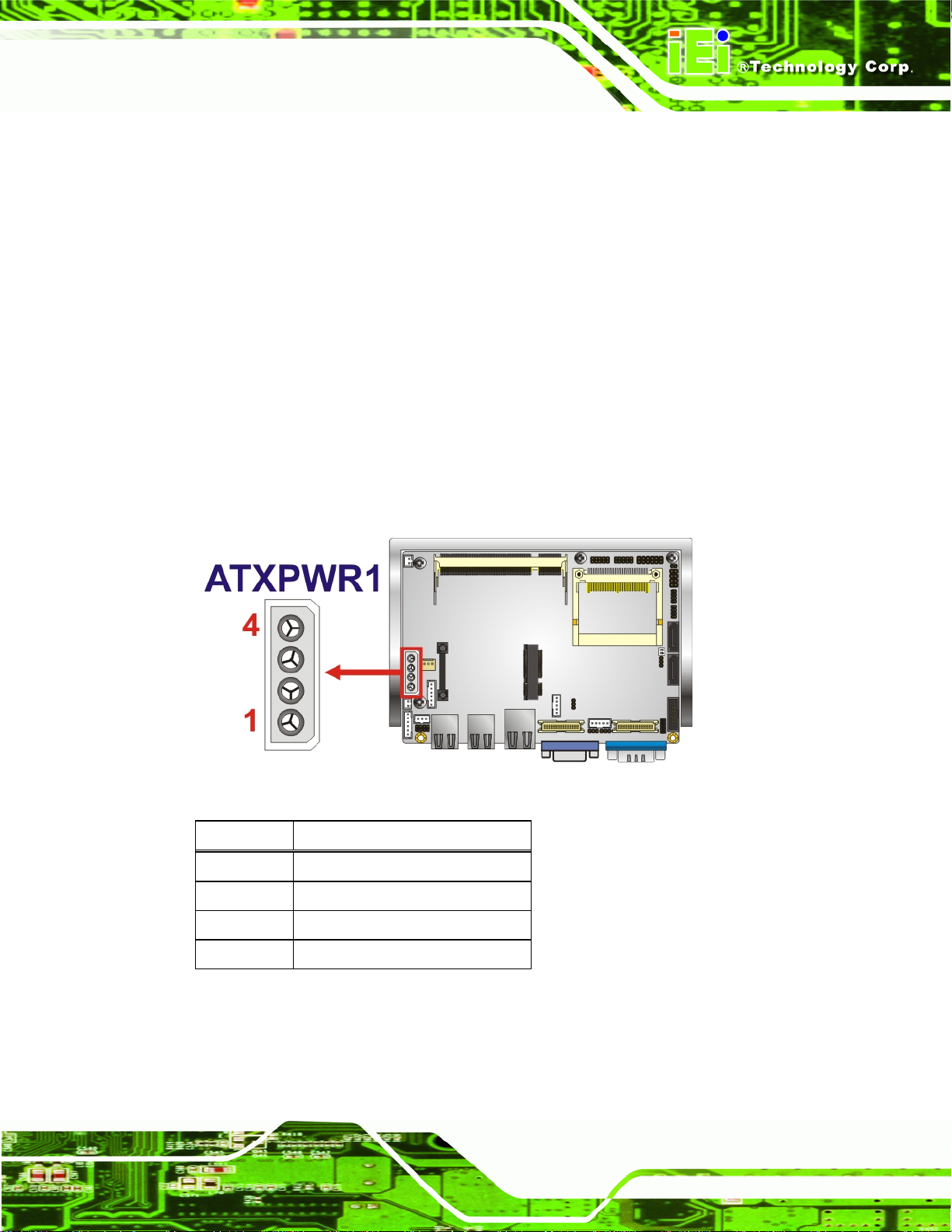
3.3.1 ATX Power Connector
CN Label: ATXPWR1
CN Type:
CN Location:
CN Pinouts:
The 4-pin ATX power connector is connected to an ATX power supply.
Figure 3-2: ATX Power Connector Location
4-pin AT power connector (1x4)
Figure 3-2
See
Table 3-3
See
Pin Description
1 +12V
2 GND
3 GND
4 +5V
Table 3-3: ATX Power Connector Pinouts
3.3.2 ATX Power Control Connector
CN Label: ATXCTL1
Page 15
Page 28
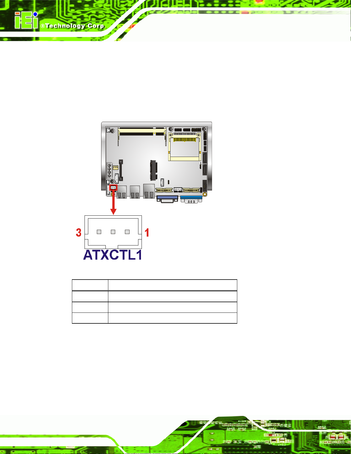
WAFER-945GSELVDS2
CN Type:
CN Location:
CN Pinouts:
Short pins 2-3 for AT power use, or connect to power control cable for ATX power control
use.
3-pin wafer (1x3)
Figure 3-3
See
Table 3-4
See
Figure 3-3: ATX Power Control Connector Location
Pin Description
1 +5V Standby
2 GND
3 PS_ON#
Table 3-4: ATX Power Supply Enable Connector Pinouts
3.3.3 Audio Connector
CN Label: AUDIO1
CN Type:
CN Location:
Page 16
10-pin header
Figure 3-4
See
Page 29
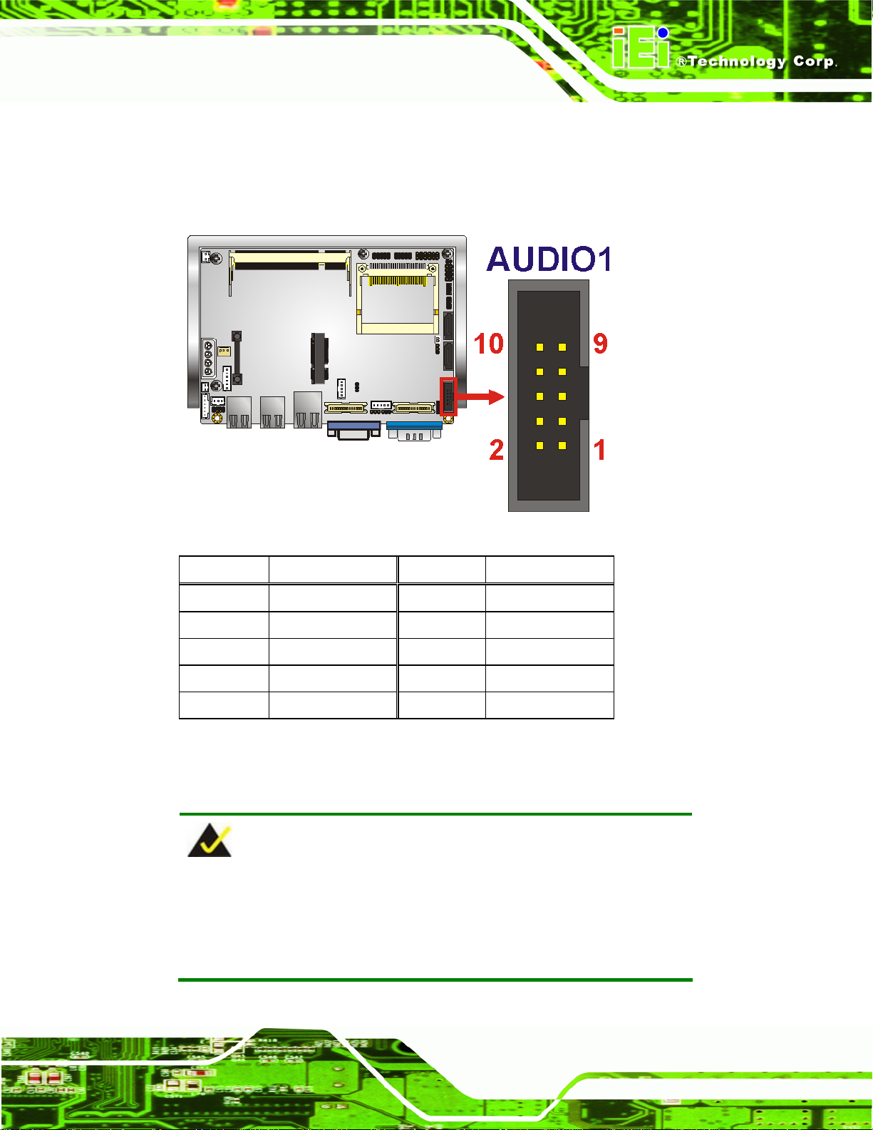
WAFER-945GSELVDS2
CN Pinouts:
The 10-pin audio connector is connected to external audio devices including speakers a nd
microphones for the input and output of audio signals to and from the system.
See
Table 3-5
Figure 3-4: Audio Connector Pinouts
Pin Description Pin Description
1 Line out R 2 Line in R
3 GND 4 GND
5 Line out L 6 Line in L
7 GND 8 GND
9 MIC in 10 Mic in
Table 3-5: Audio Connector Pinouts
3.3.4 Battery Connector
NOTE:
Attach the battery to the board or enclosure before use. Only the
battery cable is connected before shipping, but battery must also be
attached to a surface.
Page 17
Page 30
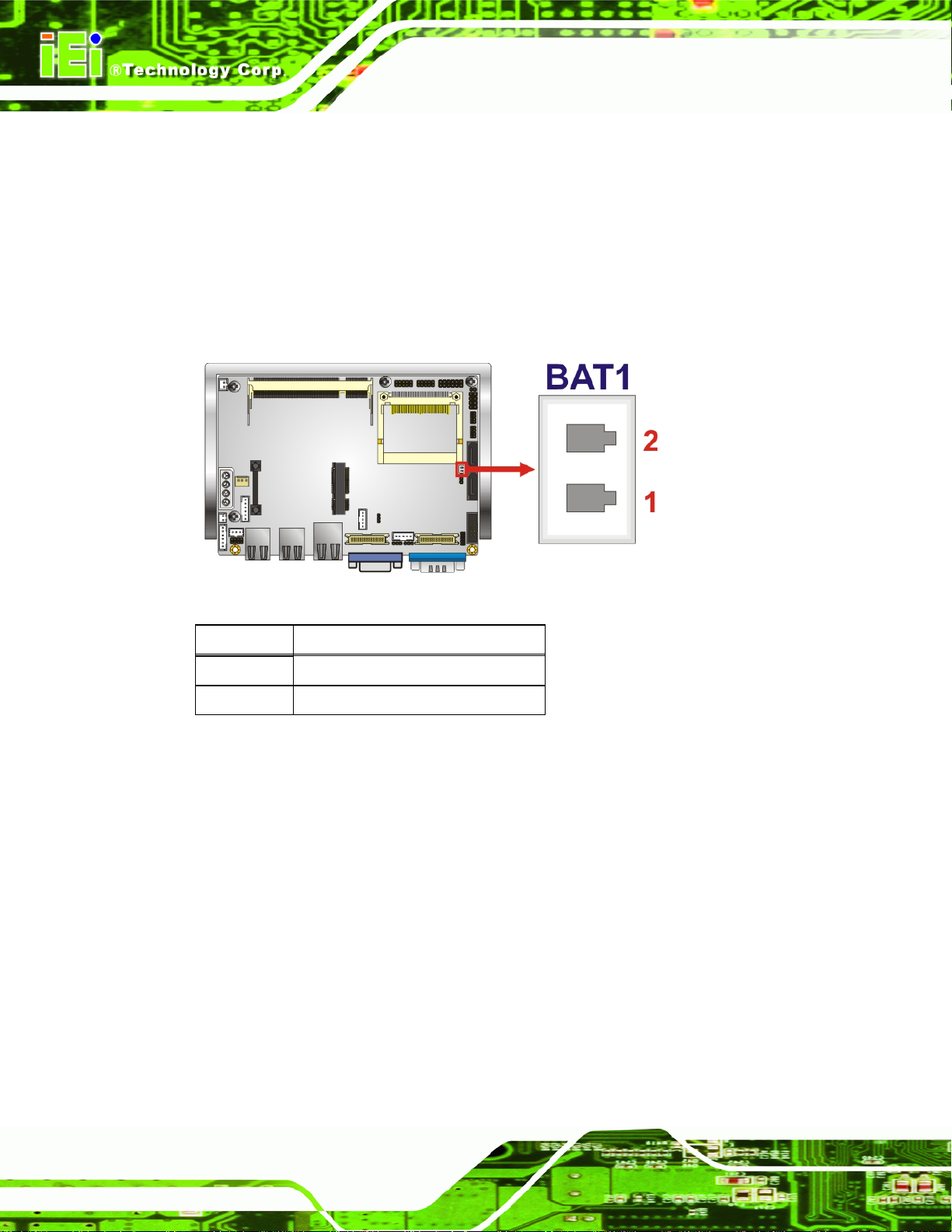
CN Label: BAT1
WAFER-945GSELVDS2
CN Type:
CN Location:
CN Pinouts:
This is connected to the system battery. The battery provides power to the system clock to
retain the time when power is turned off.
Figure 3-5: Battery Connector Location
2-pin wafer (1x2)
Figure 3-5
See
Table 3-6
See
Pin Description
1 Battery+
2 Ground
Table 3-6: Battery Connector Pinouts
3.3.5 CompactFlash® Slot
CN Label: CF1
CN Type:
CN Location:
CN Pinouts:
Used for installing a CompactFlash® card.
50-pin header (2x25)
Figure 3-6
See
Table 3-7
See
Page 18
Page 31

WAFER-945GSELVDS2
Figure 3-6: CF Card Slot Location
Pin Description Pin Description
1 GND 26 CD1#
2 D3 27 D11
3 D4 28 D12
4 D5 29 D13
5 D6 30 D14
6 D7 31 D15
7 CE# 32 CE2#
8 A10 33 VS1#
9 OE# 34 IOR#
10 A9 35 IOW#
11 A8 36 WE#
12 A7 37 IRQ
13 VCC 38 VCC
14 A6 39 CSEL#
15 A5 40 VS2#
Page 19
Page 32

Pin Description Pin Description
16 A4 41 RESET#
17 A3 42 WAIT#
18 A2 43 INPACK#
19 A1 44 REG#
20 A0 45 BVD2
21 D0 46 BVD1
22 D1 47 D8
23 D2 48 D9
24 IOCS16# 49 D10
25 CD2# 50 GND2
Table 3-7: CF Card Slot Pinouts
3.3.6 Digital I/O Connector
WAFER-945GSELVDS2
CN Label: DIO1
CN Type:
CN Location:
CN Pinouts:
10-pin header (2x5)
Figure 3-7
See
Table 3-8
See
The digital input/output connector is managed through a Super I/O chip. The DIO
connector pins are user programmable.
Page 20
Page 33

WAFER-945GSELVDS2
Figure 3-7: Digital I/O Connector Location
Pin Description Pin Description
1 GND 2 VCC
3 Output 3 4 Output 2
5 Output 1 6 Output 0
7 Input 3 8 Input 2
9 Input 1 10 Input 0
Table 3-8: Digital I/O Connector Location
3.3.7 CPU Fan Connector
CN Label: CPU_FAN1
CN Type:
CN Location:
CN Pinouts:
Connects to a CPU fan.
3-pin header
Figure 3-8
See
Table 3-9
See
Page 21
Page 34

Figure 3-8: CPU Fan Connector Location
WAFER-945GSELVDS2
Pin Description
1 GND
2 +12V
3 Fan Speed Detect
Table 3-9: CPU Fan Connector Pinouts
3.3.8 Keyboard/Mouse Connector
CN Label: KB_MS1
CN Type:
CN Location:
CN Pinouts:
The keyboard and mouse connector can be connected to a standard PS/2 cable or PS/2
Y-cable to add keyboard and mouse functionality to the system.
6-pin header (1x6)
Figure 3-9
See
Table 3-10
See
Page 22
Page 35

WAFER-945GSELVDS2
Figure 3-9: Keyboard/Mouse Connector Location
Pin Description
1 VCC (+5 V)
2 MS DATA
3 MS CLK
4 KB DATA
5 KB CLK
6 GROUND
Table 3-10: Keyboard/Mouse Connector Pinouts
3.3.9 LED Connector
CN Label: LED_C1
CN Type:
CN Location:
CN Pinouts:
The LED connector connects to an HDD indicator LED and a power LED on the system
chassis to inform the user about HDD activity and the power on/off status of the system.
6-pin wafer (1x6)
Figure 3-10
See
Table 3-11
See
Page 23
Page 36

WAFER-945GSELVDS2
Figure 3-10: LED Connector Locations
Pin Description
1 +5V
2 GND
3 Power LED+
4 Power LED5 HDD LED+
6 HDD LED-
Table 3-11: LED Connector Pinouts
3.3.10 LVDS1 LCD Connector
CN Label: LVDS1
CN Type:
CN Location:
CN Pinouts:
The 18-bit, dual-channel LVDS connector can be attached to any compatible LVDS
monitor.
30-pin crimp (2x15)
Figure 3-11
See
Table 3-12
See
Page 24
Page 37

WAFER-945GSELVDS2
Figure 3-11: LVDS1 Location
Pin Description Pin Description
1 GND1 2 GND2
3 A_Y0 4 A_Y0#
5 A_Y1 6 A_Y1#
7 A_Y2 8 A_Y2#
9 A_CK 10 A_CK#
11 NC 12 NC
13 GND3 14 GND4
15 B_Y0 16 B_Y0#
17 B_Y1 18 B_Y1#
19 B_Y2 20 B_Y2#
21 B_CK 22 B_CK#
23 NC 24 NC
25 GND5 26 GND6
27 VCC_LCD 28 VCC_LCD
29 VCC_LCD 30 VCC_LCD
Table 3-12: LVDS1 Pinouts
Page 25
Page 38

3.3.11 LVDS1 Inverter Connector
CN Label: INVERTER1
WAFER-945GSELVDS2
CN Type:
CN Location:
CN Pinouts:
Provides power to an LVDS monitor.
Figure 3-12: Backlight Connector Pinout Locations
5-pin wafer (1x5)
Figure 3-12
See
Table 3-13
See
Pin Description
1 LCD Backlight Control
2 GROUND
3 +12V
4 GROUND
5 BACKLIGHT Enable
Table 3-13: Backlight Connector Pinouts
3.3.12 LVDS2 LCD Connector
CN Label: LVDS2
30-pin crimp (2x15)
Figure 3-13
See
Page 26
CN Type:
CN Location:
Page 39

WAFER-945GSELVDS2
CN Pinouts:
The 18-bit, dual-channel LVDS connector can be attached to any compatible LVDS
monitor.
See
Table 3-14
Figure 3-13: LVDS2 Location
Pin Description Pin Description
1 GND1 2 GND2
3 A_Y0 4 A_Y0#
5 A_Y1 6 A_Y1#
7 A_Y2 8 A_Y2#
9 A_CK 10 A_CK#
11 A_Y3 12 A_Y3#
13 GND3 14 GND4
15 B_Y0 16 B_Y0#
17 B_Y1 18 B_Y1#
19 B_Y2 20 B_Y2#
21 B_CK 22 B_CK#
23 B_Y3 24 B_Y3#
25 GND5 26 GND6
27 VCC_LCD 28 VCC_LCD
Page 27
Page 40

Pin Description Pin Description
29 VCC_LCD 30 VCC_LCD
Table 3-14: LVDS2 Pinouts
3.3.13 LVDS2 Inverter Connector
CN Label: INVERTER2
WAFER-945GSELVDS2
CN Type:
CN Location:
CN Pinouts:
5-pin wafer (1x5)
Figure 3-12
See
Table 3-13
See
Provides power to an LVDS monitor.
Page 28
Figure 3-14: Backlight Connector Pinout Locations
Pin Description
1 LCD Backlight Control
2 GROUND
3 +12V
4 GROUND
Page 41

WAFER-945GSELVDS2
Pin Description
5 BACKLIGHT Enable
Table 3-15: Backlight Connector Pinouts
3.3.14 PCIe Mini Card Slot
CN Label: CN4
CN Type:
CN Location:
CN Pinouts:
52-pin Mini PCIe Card Slot
Figure 3-15
See
Table 3-16
See
The PCIe mini card slot enables a PCIe mini card expansion module to be connected to
the board. Cards supported include among others wireless LAN (WLAN) cards.
Figure 3-15: PCIe Mini Card Slot Location
Pin Description Pin Description
1 PCIE_WAKE# 2 VCC3
3 N/C 4 GND
5 N/C 6 1.5V
Page 29
Page 42

Pin Description Pin Description
7 CLKREQ# 8 N/C
9 GND 10 N/C
11 CLK- 12 N/C
13 CLK+ 14 N/C
15 GND 16 N/C
17 N/C 18 GND
19 N/C 20 VCC3
21 GND 22 PCIRST#
23 PERN2 24 3VDual
25 PERP2 26 GND
27 GND 28 1.5V
29 GND 30 SMBCLK
31 PETN2 32 SMBDATA
WAFER-945GSELVDS2
33 PETP2 34 GND
35 GND 36 USBD37 N/C 38 USBD+
39 N/C 40 GND
41 N/C 42 N/C
43 N/C 44 RF_LINK#
45 N/C 46 BLUELED#
47 N/C 48 1.5V
49 N/C 50 GND
51 N/C 52 VCC3
Table 3-16: PCIe Mini Card Slot Pinouts
3.3.15 Power Button Connector
CN Label: PWRBTN1
CN Type:
2-pin wafer (1x2)
Page 30
CN Location:
CN Pinouts:
Figure 3-16
See
Table 3-17
See
Page 43

WAFER-945GSELVDS2
Turns the system on and off when the system is set to ATX power mode.
Figure 3-16: Power Button Connector Location
Pin Description
1 Power Switch
2 GND
Table 3-17: Power Button Connector Pinouts
3.3.16 Reset Button Connector
CN Label: RESET1
CN Type:
CN Location:
CN Pinouts:
Used to reset the system when set to use ATX power.
2-pin wafer (1x2)
Figure 3-17
See
Table 3-18
See
Page 31
Page 44

Figure 3-17: Reset Button Connector Locations
WAFER-945GSELVDS2
Pin Description
1 Reset Switch
2 GND
Table 3-18: Reset Button Connector Pinouts
3.3.17 SATA Drive Connectors
CN Label: SATA1, SATA2
CN Type:
CN Location:
CN Pinouts:
The SATA drive connectors can be connected to SATA drives and support up to 3.0 Gb/s
data transfer rate.
7-pin SATA drive connectors
Figure 3-18
See
Table 3-19
See
Page 32
Page 45

WAFER-945GSELVDS2
Figure 3-18: SATA Drive Connector Locations
Pin Description
1 GND
2 TX+
3 TX4 GND
5 RX6 RX+
7 GND
Table 3-19: SATA Drive Connector Pinouts
3.3.18 Serial Port Connector
CN Label: COM3, COM4
CN Type:
CN Location:
CN Pinouts:
Provide an RS-232 communications connection.
10-pin header
Figure 3-19
See
Table 3-20
See
Page 33
Page 46

WAFER-945GSELVDS2
Figure 3-19: Serial Port Connector Location
Pin Description Pin Description
1 DCD# 2 DSR#
3 RXD 4 RTS#
5 TXD 6 CTS#
7 DTR# 8 RI#
9 GND 10 GND
Table 3-20: Serial Port Pinouts
3.3.19 Serial Port Connector (RS-232/422/485)
CN Label: COM2
CN Type:
CN Location:
CN Pinouts:
The 14-pin serial port connector connects to the COM2 serial communications channels.
COM2 is a multi function channel. In default mode COM2 is an RS-232 serial
14-pin header (2x7)
Figure 3-20
See
Table 3-21
See
Page 34
communication channel but, with the COM2 function select jumper, can be configured as
either an RS-422 or RS-485 serial communications channel.
Page 47

WAFER-945GSELVDS2
Figure 3-20: RS-232/422/485 Serial Port Connector Location
Pin Description Pin Description
1 DCD# 2 DSR#
3 RXD 4 RTS#
5 TXD 6 CTS#
7 DTR# 8 RI#
9 GND 10 N/C
11 TXD485+ 12 TXD48513 RXD485+ 14 RXD485-
Table 3-21: RS-232/RS-485 Serial Port Connector Pinouts
3.3.20 USB Connector
CN Label: USB01
CN Type:
CN Location:
CN Pinouts:
8-pin header (2x4)
Figure 3-21
See
Table 3-22
See
Page 35
Page 48

The 2x4 USB pin connectors each provide connectivity to two USB 1.1 or two USB 2.0
ports. Each USB connector can support two USB devices. Additional external USB ports
are found on the rear panel. The USB ports are used for I/O bus expansion.
Figure 3-21: USB Connector Pinout Locations
WAFER-945GSELVDS2
Pin Description Pin Description
1 VCC 2 GND
3 DATA- 4 DATA+
5 DATA+ 6 DATA7 GND 8 VCC
Table 3-22: USB Port Connector Pinouts
3.4 External Peripheral Interface Connector Panel
Page 36
Figure 3-22: WAFER-945GSELVDS2 External Peripheral Interface Connector
Page 49

WAFER-945GSELVDS2
3.4.1 LAN Connectors
CN Label: LAN1
CN Type:
CN Location:
CN Pinouts:
The WAFER-945GSELVDS2 is equipped with two built-in RJ-45 Ethernet controllers. The
controllers can connect to the LAN through two RJ-45 LAN connectors. There are two
LEDs on the connector indicating the status of LAN. The pin assignments are listed in the
following table:
Pin Description Pin Description
1 MDIA3- 5 MDIA1+
2 MDIA3+ 6 MDIA2+
3 MDIA2- 7 MDIA04 MDIA1- 8 MDIA0+
Table 3-23: LAN Pinouts
RJ-45
Figure 3-22
See
Table 3-23
See
Figure 3-23: RJ-45 Ethernet Connector
The RJ-45 Ethernet connector has two status LEDs, one green and one yello w. The green
LED indicates activity on the port and the yellow LED indicates the port is linked. See
Table 3-24.
STATUS DESCRIPTION STATUS DESCRIPTION
Green Activity Yellow Linked
Table 3-24: RJ-45 Ethernet Connector LEDs
Page 37
Page 50

3.4.2 Serial Port Connector
CN Label: COM1
WAFER-945GSELVDS2
CN Type:
CN Location:
CN Pinouts:
The 9-pin DB-9 serial port connectors are connected to RS-232 serial communications
devices.
Pin Description Pin Description
1 DCD# 6 DSR#
2 RX 7 RTS#
3 TX 8 CTS#
4 DTR# 9 RI#
5 GND
Table 3-25: Serial Port Pinouts
DB-9 connectors
Figure 3-22
See
Table 3-25 and Figure 3-24
See
Figure 3-24: Serial Port Pin Location
3.4.3 USB Connectors
CN Label: USB_C45
CN Type:
CN Location:
CN Pinouts:
The WAFER-945GSELVDS2 has two external USB 2.0 ports. The ports connect to both
USB 2.0 and USB 1.1 devices.
Page 38
Dual USB port
Figure 3-22
See
Table 3-26
See
Page 51

WAFER-945GSELVDS2
Pin Description Pin Description
1 VCC (+5V) 5 VCC (+5V)
2 DATA4- 6 DATA53 DATA4+ 7 DATA5+
4 GND 8 GND
Table 3-26: USB Port Pinouts
3.4.4 VGA Connector
CN Label: VGA1
CN Type:
CN Location:
CN Pinouts:
15-pin Female
Figure 3-22
See
Figure 3-25 and Table 3-27
See
The WAFER-945GSELVDS2 has a single 15-pin female connector for connectivity to
standard display devices.
Figure 3-25: VGA Connector
Pin Description Pin Description
1 RED 2 GREEN
3 BLUE 4 NC
5 GND 6 CRT_PLUG7 GND 8 GND
9 VCC 10 GND
11 NC 12 DDC DAT
13 HSYNC 14 VSYNC
15 DDCCLK
Table 3-27: VGA Connector Pinouts
Page 39
Page 52

WAFER-945GSELVDS2
Chapter
4
4 Installation
Page 40
Page 53

WAFER-945GSELVDS2
4.1 Anti-static Precautions
WARNING:
Failure to take ESD precautions during the installation of the
WAFER-945GSELVDS2 may result in permanent damage to the
WAFER-945GSELVDS2 and severe injury to the user.
Electrostatic discharge (ESD) can cause serious damage to electronic components,
including the WAFER-945GSELVDS2. Dry climates are especially susceptible to ESD. It
is therefore critical that whenever the WAFER-945GSELVDS2, or any other electrical
component is handled, the following anti-static precautions are strictly adhered to.
Wear an anti-static wristband: - Wearing a simple anti-static wristband can
help to prevent ESD from damaging the board.
Self-grounding:- Before handling the board touch any grounded conducting
material. During the time the board is handled, frequently touch any
conducting materials that are connected to the ground.
Use an anti-static pad: When configuring the WAFE R-945GSELVDS2, place
it on an antic-static pad. This reduces the possibility of ESD damaging the
WAFER-945GSELVDS2.
Only handle the edges of the PCB:-: When handling the PCB, hold the PCB
by the edges.
Page 41
Page 54

4.2 Installation Considerations
NOTE:
The following installation notices and installation considerations should
be read and understood before the WAFER-945GSELVDS2 is
installed. All installation notices pertaining to the installation of the
WAFER-945GSELVDS2 should be strictly adhered to. Failing to
adhere to these precautions may lead to severe damage of the
WAFER-945GSELVDS2 and injury to the person installing the
motherboard.
4.2.1 Installation Notices
WAFER-945GSELVDS2
WARNING:
The installation instructions described in this manual should be
carefully followed in order to prevent damage to the
WAFER-945GSELVDS2, WAFER-945GSELVDS2 components and
injury to the user.
Before and during the installation please DO the following:
Read the user manual:
o The user manual provides a complete description of the
WAFER-945GSELVDS2 installation instructions and configuration
options.
Wear an electrostatic discharge cuff (ESD):
o Electronic components are easily damaged by ESD. Wearing an ESD cuff
removes ESD from the body and helps prevent ESD damage.
Place the WAFER-945GSELVDS2 on an antistatic pad:
Page 42
o When installing or configuring the motherboard, place it on an antistatic
pad. This helps to prevent potential ESD damage.
Page 55

WAFER-945GSELVDS2
Turn all power to the W A FER-945GSELVDS2 off:
o When working with the WAFER-945GSELVDS2, make sure that it is
disconnected from all power supplies and that no electricity is being fed
into the system.
Before and during the installation of the WAFER-945GSELVDS2 DO NOT:
Remove any of the stickers on the PCB board. These stickers are required for
warranty validation.
Use the product before verifying all the cables and power connectors are
properly connected.
Allow screws to come in contact with the PCB circuit, connector pins, or its
components.
4.2.2 Installation Checklist
The following checklist is provided to ensure the WAFER-945GSELVDS2 is properly
installed.
All the items in the packing list are present
A compatible memory module is properly inserted into the slot
The CF Type I or CF Type II card is properly installed i nto the CF so cket
The jumpers have been properly configured
The WAFER-945GSELVDS2 is inserted into a chassis with adequate
ventilation
The correct power supply is being used
The following devices are properly connected
o SATA drives
o Power supply
o USB cable
o Serial port cable
o Keyboard and mouse cable
The following external peripheral devices are properly connected to the
chassis:
o VGA screen
o USB devices
Page 43
Page 56

4.3 Unpacking
When the WAFER-945GSELVDS2 is unpacked, please check all the unpacking list items
listed in Chapter 3 are indeed present. If any of the unpacking list items are not available
please contact the WAFER-945GSELVDS2 vendor reseller/vendor where the
WAFER-945GSELVDS2 was purchased or contact an IEI sales representative.
4.4 SO-DIMM Installation
WARNING:
Using incorrectly specified SO-DIMM may cause permanently damage
the WAFER-945GSELVDS2. Please make sure the purchased
SO-DIMM complies with the memory specifications of the
WAFER-945GSELVDS2. SO-DIMM specifications compliant with the
WAFER-945GSELVDS2
WAFER-945GSELVDS2 are listed in Chapter 2.
To install a SO-DIMM into a SO-DIMM socket, please follow the steps below and refer to
Figure 4-1.
Figure 4-1: SO-DIMM Installation
Step 1: Locate the SO-DIMM socket. Place the WAFER-945GSELVDS2 on an
anti-static pad with the solder side facing up.
Page 44
Step 2: Align the SO-DIMM with the socket. The SO-DIMM must be oriented in such a
way that the notch in the middle of the SO-DIMM must be aligned with the
plastic bridge in the socket.
Page 57

WAFER-945GSELVDS2
Step 3: Insert the SO-DIMM. Push the SO-DIMM chip into the socket at an angle. (See
Figure 4-1)
Step 4: Open the SO-DIMM socket arms. Gently pull the arms of the SO-DIMM socket
out and push the rear of the SO-DIMM down. (See
Step 5: Secure the SO-DIMM. Release the arms on the SO-DIMM socket. They clip into
place and secure the SO-DIMM in the socket.Step 0:
4.5 CF Card Installation
NOTE:
The WAFER-945GSELVDS2 can support both CF Type I cards and CF
Type II cards. For the complete specifications of the supported CF
cards please refer to Chapter 2.
To install the a CF card (Type 1 or Type 2) onto the WAFER-945GSELVDS2, please
follow the steps below:
Figure 4-1)
Step 1: Locate the CF card socket. Place the WAFER-945 GSELVDS2 on an anti-static
pad with the solder side facing up. Locate the CF card.
Step 2: Align the CF card. Make sure the CF card is properly aligned with the CF
socket.
Step 3: Insert the CF card. Gently insert the CF card into the socket making sure the
socket pins are properly inserted into the socket. See
Figure 4-2. Step 0:
Page 45
Page 58

WAFER-945GSELVDS2
Figure 4-2: CF Card Installation
4.6 Jumper Settings
NOTE:
A jumper is a metal bridge used to close
an electrical circuit. It consists of two or
three metal pins and a small metal clip
(often protected by a plastic cover) that
slides over the pins to connect them. To
CLOSE/SHORT a jumper means
connecting the pins of the jumper with
the plastic clip and to OPEN a jumper means removing the plastic clip
from a jumper.
Page 46
Page 59

WAFER-945GSELVDS2
Before the WAFER-945GSELVDS2 is installed in the system, the jumpers must be set in
accordance with the desired configuration. The jumpers on the WAFER-945GSELVDS2
are listed in
Description Label Type
AT Power Mode Setting ATXCTL1 2-pin header
Audio Power Source JP2 3-pin header
CF Card Setting JCF1 2-pin header
Clear CMOS J_CMOS1 3-pin header
COM2 Mode Setting JP1 6-pin header
LVDS1 Panel Resolution J_LCD_TYPE1 8-pin header
LVDS1 voltage selection J_VLVDS1 3-pin header
LVDS2 voltage selection J_VLVDS2 3-pin header
Table 4-1: Jumpers
Table 4-1.
4.6.1 AT Power Select Jumper Settings
NOTE:
The AT Power Select Jumper is the same as the ATX Enable
connector.
Jumper Label: ATXCTL1
Jumper Type:
Jumper Settings:
Jumper Location:
Sets the system to use AT or ATX power. When set to ATX power, the power switch cable
must be connected to this jumper.
Pin Description
2-3 Use AT power
3-pin header
Table 4-2
See
Figure 4-3
See
Page 47
Page 60

Pin Description
Open Use ATX power
WAFER-945GSELVDS2
Table 4-2: AT Power Select Jumper Settings
The location of the AT Power Select jumper is shown in Figure 4-3 below.
Figure 4-3: AT Power Select Jumper Location
4.6.2 Audio Power Source
Jumper Label: JP2
Jumper Type:
Jumper Settings:
Jumper Location:
Sets the power source for the onboard audio. The 12 V power converted to 5 V through a
regulator may provide a cleaner power signal, which will in turn give an audio signal with
less background noise.
Pin Description
1-2 Power through 5 V
2-3 Power through 12 V to 5 V regulator
3-pin header
Table 4-3
See
Figure 4-4
See
Page 48
Table 4-3: Audio Power Source
Page 61

WAFER-945GSELVDS2
The location of the audio power source selection jumper is shown below.
Figure 4-4: Audio Power Source
4.6.3 CF Card Setup
Jumper Label: JCF1
Jumper Type:
Jumper Settings:
Jumper Location:
The CF Card Setup jumper sets the CF Type I card or CF Type II cards as either the slave
device or the master device. CF Card Setup jumper settings are shown in
Pin Description
Open Slave
Short Master
Table 4-4: CF Card Setup Jumper Settings
The CF Card Setup jumper location is shown in Figure 4-5.
2-pin header
Table 4-4
See
Figure 4-5
See
Table 4-4.
Page 49
Page 62

Figure 4-5: CF Card Setup Jumper Location
4.6.4 Clear CMOS Jumper
Jumper Label: J_CMOS1
WAFER-945GSELVDS2
Jumper Type:
Jumper Settings:
Jumper Location:
If the WAFER-945GSELVDS2 fails to boot due to improper BIOS settings, the clear
CMOS jumper clears the CMOS data and resets the system BIOS information. To do this,
use the jumper cap to close pins 2 and 3 for a few seconds then reinstall the jumper clip
back to pins 1 and 2.
If the “CMOS Settings Wrong” message is displayed during the boot up process, the fault
may be corrected by pressing the F1 to enter the CMOS Setup menu. Do one of the
following:
Enter the correct CMOS setting
Load Optimal Defaults
Load Failsafe Defaults.
3-pin header
Table 4-5
See
Figure 4-6
See
Page 50
After having done one of the above, save the changes and exit the CMOS Setup menu.
The clear CMOS jumper settings are shown in
Table 4-5.
Page 63

WAFER-945GSELVDS2
Pin Description
1-2 Keep CMOS Setup
2-3 Clear CMOS Setup
Table 4-5: Clear CMOS Jumper Settings
The location of the clear CMOS jumper is shown in Figure 4-6 below.
Figure 4-6: Clear CMOS Jumper
4.6.5 COM2 Mode Selection
Jumper Label: JP1
Jumper Type:
Jumper Settings:
Jumper Location:
The COM 2 Function Select jumper sets the communication protocol used by the second
serial communications port (COM 2) as RS-232, RS-422 or RS -485. The COM 2 Function
Select settings are shown in
Pin Description
1-2 RS-232
3-4 RS-422
5-6 RS-485
5-6 & 7-8 RS-485 with RTS control
8-pin header
Table 4-6
See
Figure 4-7
See
Table 4-6.
Table 4-6: COM 2 Function Select Jumper Settings
The COM 2 Function Select jumper location is shown in Figure 4-7.
Page 51
Page 64

Figure 4-7: COM 2 Function Select Jumper Location
4.6.6 LVDS1 and LVDS2 Panel Resolution Jumper
Jumper Label: J_LCD_TYPE1
WAFER-945GSELVDS2
Jumper Type:
Jumper Settings:
Jumper Location:
8-pin header
Table 4-7
See
Figure 4-8
See
Sets the resolution of both LVDS1 and LVDS2 video channels.
Pin LVDS1 Resolution
Open 800 x 600, 18-bit
1-2 1024 x 768, 18-bit
3-4 1280 x 1024, 36-bit
1-2, 3-4 1400 x 1050, 36-bit
Table 4-7: LVDS1 Panel Resolution
Pin LVDS2 Resolution
Open 1024 x 768, 18-bit
5-6 1024 x 768, 24-bit
7-8 1280 x 1024, 36-bit
Page 52
5-6, 7-8 1280 x 1024, 48-bit
Table 4-8: LVDS2 Panel Resolution
The LVDS Panel Resolution jumper location. is shown in Figure 4-8.
Page 65

WAFER-945GSELVDS2
Figure 4-8:LVDS Panel Resolution Jumper Pinout Locations
4.6.7 LVDS1 Voltage Selection
WARNING:
Permanent damage to the screen and WAFER-945GSELVDS2 may
occur if the wrong voltage is selected with this jumper. Please refer to
the user guide that came with the monitor to select the correct voltage.
Jumper Label: J_VLVDS1
Jumper Type:
Jumper Settings:
Jumper Location:
Sets the voltage provided to the monitor by LVDS1.
Pin Description
3-pin header
See
See
Table 4-9
Figure 4-9
1-2 +3.3V LVDS
2-3 +5V LVDS
Table 4-9: LVDS Voltage Selection Jumper Settings
Page 53
Page 66

The LVDS1 Voltage Selection jumper location. is shown in Figure 4-9.
Figure 4-9: LVDS1 Voltage Selection Jumper Pinout Locations
4.6.8 LVDS2 Voltage Selection
WARNING:
WAFER-945GSELVDS2
Permanent damage to the screen and WAFER-945GSELVDS2 may
occur if the wrong voltage is selected with this jumper. Please refer to
the user guide that cam with the monitor to select the correct voltage.
Jumper Label: J_VLVDS2
Jumper Type:
Jumper Settings:
Jumper Location:
Sets the voltage provided to the monitor connected to LVDS2
Pin Description
1-2 +3.3V LVDS
2-3 +5V LVDS
Table 4-10: LVDS2 Voltage Selection Jumper Settings
3-pin header
Table 4-10
See
Figure 4-10
See
Page 54
The LVDS2 Voltage Selection jumper location. is shown in Figure 4-9.
Page 67

WAFER-945GSELVDS2
Figure 4-10: LVDS Voltage Selection Jumper Pinout Locations
4.7 Chassis Installation
4.7.1 Airflow
WARNING:
Airflow is critical to the cooling of the CPU and other onboard
components. The chassis in which the WAFER-945GSELVDS2 must
have air vents to allow cool air to move into the system and hot air to
move out.
The WAFER-945GSELVDS2 must be installed in a chassis with ventilation holes on the
sides allowing airflow to travel through the heat sink surface. In a system with an individual
power supply unit, the cooling fan of a power supply can also help generate airflow
through the board surface.
NOTE:
IEI has a wide range of backplanes available. Please contact your
WAFER-945GSELVDS2 vendor, reseller or an IEI sales representative
at
(
sales@iei.com.tw or visit the IEI website
http://www.ieiworld.com.tw) to find out more about the available
chassis.
Page 55
Page 68

4.7.2 Motherboard Installation
To install the WAFER-945GSELVDS2 motherboard into the chassis please refer to the
reference material that came with the chassis.
4.8 Internal Peripheral Device Connections
Install the following cables to use the internal devices listed.
4.8.1 Audio Kit Installation
The Audio Kit that came with the WAFER-945GSELVDS2 connects to the audio
connector on the WAFER-945GSELVDS2. The audio kit consists of three audio jacks.
Mic-in connects to a microphone. Line-in provides a stereo line-level input to connect to
the output of an audio device. Line-out, a stereo line-level output, connects to two
amplified speakers. To install the audio kit, please refer to the steps below:
WAFER-945GSELVDS2
Step 1: Locate the audio connector. The location of the 10-pin audi o connector is
shown in Chapter 3.
Step 2: Align pin 1. Align pin 1 on the on-board connector with pin 1 on the audio kit
connector. Pin 1 on the audio kit connector is indicated with a white dot.
Page 56
Page 69

WAFER-945GSELVDS2
Figure 4-11: Audio Kit Cable Connection
Step 3: Connect the audio devices. Connect speakers to the line-out audio jack.
Connect the output of an audio device to the line-in audio jack. Connect a
microphone to the mic-in audio jack.Step 0:
4.8.2 SATA Drive Connection
The WAFER-945GSELVDS2 is shipped with two SATA drive cables and one SATA drive
power cable. To connect the SATA drives to the connectors, please follow the steps
below.
Step 1: Locate the connectors. The locations of the SATA drive connectors are shown
in Chapter 3.
Page 57
Page 70

Step 2: Insert the cable connector. Press the clip on the connector at the end of the
SATA cable and insert the cable connector into the onboard SATA drive
WAFER-945GSELVDS2
connector. See
Figure 4-12.
Figure 4-12: SATA Drive Cable Connection
Step 3: Connect the cable to the SATA disk. Connect the connector on the other end
of the cable to the connector at the back of the SATA drive. See
Figure 4-13.
NOTE:
The SATA power cable described below is an optional item and must
be pre-ordered. The SATA power cable is not shipped with the system.
Step 4: Connect the SATA power cable. Connect the SATA power connector to the
back of the SATA drive. See
Figure 4-13. Step 0:
Page 58
Page 71

WAFER-945GSELVDS2
Figure 4-13: SATA Power Drive Connection
4.8.3 RS-232 Cable Connection
The dual RS-232 cable consists of two connectors attached to two independent cables.
Each cable is then attached to a D-sub 9-pin male connector. To install the dual RS-232
cable, please follow the steps below.
Step 1: Locate the connectors. The locations of the RS-232 connectors are shown in
Chapter 3.
Step 2: Insert the cable connectors. Insert one connector into each serial port box
headers. See Figure 5-13. A key on the front of the cable connectors ensures
the connector can only be installed in one direction.
Page 59
Page 72

Figure 4-14: Dual RS-232 Cable Installation
Step 3: Secure the connectors. Both single RS-232 connectors have two retention
WAFER-945GSELVDS2
screws that must be secured to a chassis or bracket.
Step 4: Connect the serial device. Once the single RS-232 connectors are connected
to a chassis or bracket, a serial communications device can be connecte d to the
system. Step 0:
4.8.4 Keyboard/Mouse Y-cable Connector
The WAFER-945GSELVDS2 is shipped with a keyboard/mouse Y-cable connector. The
keyboard/mouse Y-cable connector connects to a keyboard/mouse connector on the
WAFER-945GSELVDS2 and branches into two cables that are each connected to a PS/2
connector, one for a mouse and one for a keyboard. To connect the keyboard/mouse
Y-cable connector please follow the steps below.
Step 1: Locate the connector. The location of the keyboard/mouse Y-cable connector
is shown in Chapter 3.
Step 2: Align the connectors. Correctly align pin 1 on the cable connector with pin 1 on
Page 60
the WAFER-945GSELVDS2 keyboard/mouse connector. See
Figure 4-15.
Page 73

WAFER-945GSELVDS2
Step 3: Insert the cable connectors. Once the cable connector is p rope rly aligne d wit h
the keyboard/mouse connector on the WAFER-945GSELVDS2, connect the
cable connector to the on-board connectors. See
Figure 4-15.
Figure 4-15: Keyboard/mouse Y-cable Connection
Step 4: Attach PS/2 connectors to the chassis. The keyboard/mouse Y-cable
connector is connected to two PS/2 connectors. To secure the PS/2 connectors
to the chassis please refer to the installation instructions that came with the
chassis.
Step 5: Connect the keyboard and mouse. Once the PS/2 connectors are connected
to the chassis, a keyboard and mouse can each be connected to one of the
PS/2 connectors. The keyboard PS/2 connector and mouse PS/2 connector are
both marked. Please make sure the keyboard and mouse are connected to the
correct PS/2 connector. Step 0:
Page 61
Page 74

4.8.5 USB Cable
The WAFER-945GSELVDS2 is shipped with a dual port USB 2.0 cable. To connect the
USB cable connector, please follow the steps below.
Step 1: Locate the connectors. The locations of the USB connectors are shown in
WARNING:
Step 2: Align the connectors. The cable has two connectors. Correctly align pin 1on
WAFER-945GSELVDS2
Chapter 3.
If the USB pins are not properly aligned, the USB device can burn out.
each cable connector with pin 1 on the WAFER-945GSELVDS2 USB connector.
Step 3: Insert the cable connectors. Once the cable connectors are properly aligned
with the USB connectors on the WAFER-945GSELVDS2, connect the cable
connectors to the on-board connectors. See
Figure 4-16: Dual USB Cable Connection
Figure 4-16.
Page 62
Step 4: Attach the USB connectors to the chassis. The USB 2.0 connectors each of
two retention screw holes. To secure the connectors to the chassis please refer
to the installation instructions that came with the chassis.Step 0:
Page 75

WAFER-945GSELVDS2
4.9 External Peripheral Interface Connection
This section outlines the installation of devices to the external ports on the
WAFER-945GSELVDS2.
4.9.1 LAN Connection (Single Connector)
There are two external RJ-45 LAN connectors. The RJ-45 connectors enable connection
to an external network. To connect a LAN cable with an RJ-45 connector, please follow
the instructions below.
Step 1: Locate the RJ-45 connectors. The locations of the USB connecto rs are shown
in Chapter 4.
Step 2: Align the connectors. Align the RJ-45 connector on the LAN cable with one of
the RJ-45 connectors on the WAFER-945GSELVDS2. See
Figure 4-17: LAN Connection
Figure 4-17.
Step 3: Insert the LAN cable RJ-45 connector . Once aligned, gently insert the LAN cable
RJ-45 connector into the onboard RJ-45 connector.Step 0:
Page 63
Page 76

4.9.2 Serial Device Connection
The WAFER-945GSELVDS2 has a single female DB-9 connector on the external
peripheral interface panel for a serial device. Follow the steps below to connect a serial
device to the WAFER-945GSELVDS2.
Step 1: Locate the DB-9 connector. The location of the DB-9 connector is shown in
Chapter 3.
Step 2: Insert the serial connector. Insert the DB-9 connector of a serial device into
WAFER-945GSELVDS2
the DB-9 connector on the external peripheral interface. See
Figure 4-18.
Figure 4-18: Serial Device Connector
Step 3: Secure the connector. Secure the serial device connector to the external
interface by tightening the two retention screws on either side of the connector.
4.9.3 USB Connection (Dual Connector)
The external USB Series "A" receptacle connectors provide easier and quicker access to
external USB devices. Follow the steps below to connect USB devices to the
WAFER-945GSELVDS2.
Page 64
Step 0:
Page 77

WAFER-945GSELVDS2
Step 1: Locate the USB Series "A" receptacle connectors. The location of the USB
Series "A" receptacle connectors are shown in Chapter 3.
Step 2: Insert a USB Series "A" plug. Insert the USB Series "A" plug of a device into
the USB Series "A" receptacle on the external peripheral interface. See
4-19.Step 0:
Figure
Figure 4-19: USB Connector
4.9.4 VGA Monitor Connection
The WAFER-945GSELVDS2 has a single female DB-15 connector on the external
peripheral interface panel. The DB-15 connector is connected to a CRT or VGA monitor.
To connect a monitor to the WAFER-945GSELVDS2, please follow the instructions below.
Step 1: Locate the female DB-15 connector. The location of the female DB-15
connector is shown in Chapter 3.
Step 2: Align the VGA connector. Align the male DB-15 connector on the VGA screen
cable with the female DB-15 connector on the external peripheral interface.
Page 65
Page 78

Step 3: Insert the VGA connector. Once the conne ctors are prop erly aligned with the
insert the male connector from the VGA screen into the female connector on the
WAFER-945GSELVDS2
WAFER-945GSELVDS2. See
Figure 4-20: VGA Connector
Figure 4-20.
Step 4: Secure the connector. Secure the DB-15 VGA connector from the VGA monitor
to the external interface by tightening the two retention screws on either side of
the connector.Step 0:
4.10 Heat Sink Enclosure
WARNING:
Never run the WAFER-945GSELVDS2 without the heat sink secured
to the board. The heat sink ensures the system remains cool and does
not need addition heat sinks to cool the system.
Page 66
Page 79

WAFER-945GSELVDS2
WARNING:
When running the WAFER-945GSELVDS2, do not put the
WAFER-945GSELVDS2 directly on a surface that can not dissipate
system heat, especially the wooden or plastic desk. It is highly
recommended to run the WAFER-945GSELVDS2
Æ on a heat dissipation surface or
Æ using copper pillars to hold the board up from the desk below
When the WAFER-945GSELVDS2 is shipped it is secured to a heat sink with five
retention screws. If the WAFER-945GSELVDS2 must be removed from the heat sink, the
five retention screws must be removed.
Figure 4-21: Heat Sink Retention Screws
4.11 Installing Drivers
To access the driver installation programs, please do the following.
Page 67
Page 80

Step 1: Insert the CD-ROM that came with the system into a CD-ROM drive attached to
the system.
WAFER-945GSELVDS2
Step 2: The screen in
Figure 4-22: Start Up Screen
Figure 4-22 appears.
Page 68
Page 81

WAFER-945GSELVDS2
Step 3: Select the operating system.
Figure 4-23: Select Operating System
Step 4: Install all the drivers from the list. Step 0:
Figure 4-24: Drivers
Page 69
Page 82

WAFER-945GSELVDS2
Chapter
5
5 BIOS
Page 70
Page 83

WAFER-945GSELVDS2
5.1 Introduction
The BIOS is programmed onto the BIOS chip. The BIOS setup program allows changes to
certain system settings. This chapter outlines the options that can be changed.
5.1.1 Starting Setup
The AMI BIOS is activated when the computer is turned on. The setup program can be
activated in one of two ways.
1. Press the D
2. Press the D
appears on the screen. 0.
If the message disappears before the D
again.
ELETE key as soon as the system is turned on or
ELETE key when the “Press Del to enter SETUP” message
ELETE key is pressed, restart the computer and try
5.1.2 Using Setup
Use the arrow keys to highlight items, press ENTER to select, use the PageUp and
PageDown keys to change entries, press F1 for help and press E
keys are shown in.
Key Function
Up arrow Move to previous item
Down arrow Move to next item
Left arrow Move to the item on the left hand side
SC to quit. Navigation
Right arrow Move to the item on the right hand side
Esc key Main Menu – Quit and not save changes into CMOS
Status Page Setup Menu and Option Page Setup Menu --
Exit current page and return to Main Menu
Page Up key Increase the numeric value or make changes
Page Dn key Decrease the numeric value or make changes
F1 key General help, only for Status Page Setup Menu and Option
Page Setup Menu
Page 71
Page 84

Key Function
F2 /F3 key Change color from total 16 colors. F2 to select color
F10 key Save all the CMOS changes, only for Main Menu
Table 5-1: BIOS Navigation Keys
5.1.3 Getting Help
When F1 is pressed a small help window describing the appropriate keys to use and the
WAFER-945GSELVDS2
forward.
possible selections for the highlighted item appears. To exit the Help Window press E
the F1 key again.
5.1.4 Unable to Reboot After Configuration Changes
If the computer cannot boot after BIOS changes are made, the BIOS will either
automatically reset to default settings, or can be manually reset using the "Clear CMOS"
jumper.
5.1.5 BIOS Menu Bar
The menu bar on top of the BIOS screen has the following main items:
Main – Changes the basic system configuration.
Advanced – Changes the advanced system settings.
PCIPnP – Changes the advanced PCI/PnP Settings
Boot – Changes the system boot configuration.
Security – Sets User and Supervisor Passwords.
SC or
Page 72
Chipset – Changes the chipset settings.
Exit – Selects exit options and loads default settings
The following sections completely describe the configuration options found in the menu
items at the top of the BIOS screen and listed above.
Page 85

WAFER-945GSELVDS2
5.2 Main
The Main BIOS menu appears when the BIOS Se tup program is entered. The Main menu
gives an overview of the basic system information.
BIOS SETUP UTILITY
Main Advanced PCIPNP Boot Security Chipset Exit
System Overview
⎯⎯⎯⎯⎯⎯⎯⎯⎯⎯⎯⎯⎯⎯⎯⎯⎯⎯⎯⎯⎯⎯⎯⎯⎯⎯⎯⎯⎯⎯⎯
AMIBIOS
Version :08.00.15
Build Date :06/23/09
ID: :B157MR14
Processor
Genuine Intel® CPU N270 @ 1.60GHz
Speed :1600MHz
Count :1
System Memory
Size :1016MB
System Time [14:20:27]
System Time [Tue 05/06/2008]
v02.61 ©Copyright 1985-2006, American Megatrends, Inc.
Use [ENTER], [TAB] or
[SHIFT-TAB] to select a
field.
Use [+] or [-] to
configure system time.
ÅÆ
Select Screen
↑ ↓ Select Item
Enter Go to SubScreen
F1 General Help
F10 Save and Exit
ESC Exit
BIOS Menu 1: Main
System Overview
The System Overvie w lists a brief summary of different system components. Th e fields in
System Overview cannot be changed. The items shown in the system overview include:
AMI BIOS: Displays auto-detected BIOS information
o Version: Current BIOS version
o Build Date: Date the current BIOS version was made
o ID: Installed BIOS ID
Processor: Displays auto-detected CPU specifications
o Type: Names the currently installed processor
o Speed: Lists the processor speed
o Count: The number of CPUs on the motherboard
System Memory: Displays the auto-detected system memory.
o Size: Lists memory size
Page 73
Page 86

The System Overview field also has two user configurable fields:
System Time [xx:xx:xx]
Use the System Time option to set the system time. Manually enter the hours, minutes
and seconds.
System Date [xx/xx/xx]
Use the System Date option to set the system date. Manually enter the day, month and
year.
5.3 Advanced
Use the Advanced menu to configure the CPU and peripheral devices through the
following sub-menus:
WAFER-945GSELVDS2
BIOS SETUP UTILITY
Main Advanced PCIPNP Boot Security Chipset Exit
Advanced Settings
⎯⎯⎯⎯⎯⎯⎯⎯⎯⎯⎯⎯⎯⎯⎯⎯⎯⎯⎯⎯⎯⎯⎯⎯⎯⎯⎯⎯⎯⎯⎯
WARNING: Setting wrong values in below sections may
cause system to malfunction
> CPU Configuration
> IDE Configuration
> SuperIO Configuration
> Hardware Health Configuration
> Power Configuration
> Remote Access Configuration
> USB Configuration
v02.61 ©Copyright 1985-2006, American Megatrends, Inc.
BIOS Menu 2: Advanced
Configure CPU
ÅÆ
Select Screen
↑ ↓ Select Item
Enter Go to SubScreen
F1 General Help
F10 Save and Exit
ESC Exit
Page 74
Page 87

WAFER-945GSELVDS2
5.3.1 CPU Configuration
Use the CPU Configuration menu to view detailed CPU specifications and configure the
CPU.
BIOS SETUP UTILITY
Main Advanced PCIPNP Boot Security Chipset Exit
Configure Advanced CPU Settings
Module Version:3F.10
⎯⎯⎯⎯⎯⎯⎯⎯⎯⎯⎯⎯⎯⎯⎯⎯⎯⎯⎯⎯⎯⎯⎯⎯⎯⎯⎯⎯⎯⎯⎯
Manufacturer :Intel®
Genuine Intel® CPU N270 @ 1.60GHz
Frequency :1.60GHz
FSB Speed :532Hz
Cache L1 :24 KB
Cache L2 :512 KB
Ratio Actual Value:12
ÅÆ
Select Screen
↑ ↓ Select Item
Enter Go to SubScreen
F1 General Help
F10 Save and Exit
ESC Exit
v02.61 ©Copyright 1985-2006, American Megatrends, Inc.
BIOS Menu 3: CPU Configuration
The CPU Configuration menu lists the following CPU details:
Manufacturer: Lists the name of the CPU manufacturer
Brand String: Lists the brand name of the CPU being used
Frequency: Lists the CPU processing speed
FSB Speed: List s the FSB speed
Cache L1: Lists the CPU L1 cache size
Cache L2: Lists the CPU L2 cache size
Ratio actual value is the ratio of the frequency to the clock speed
Page 75
Page 88

WAFER-945GSELVDS2
5.3.2 IDE Configuration
Use the IDE Configuration menu to change and/or set the configuration of the IDE
devices installed in the system.
BIOS SETUP UTILITY
Main Advanced PCIPNP Boot Security Chipset Exit
IDE Configuration
⎯⎯⎯⎯⎯⎯⎯⎯⎯⎯⎯⎯⎯⎯⎯⎯⎯⎯⎯⎯⎯⎯⎯⎯⎯⎯⎯⎯⎯⎯⎯
ATA/IDE Configuration [Compatible]
Legacy IDE Channels [SATA Pri, PATA Sec]
> Primary IDE Master : [Not Detected]
> Primary IDE Slave : [Not Detected]
> Secondary IDE Master : [Not Detected]
> Secondary IDE Slave : [Not Detected]
Options
Disabled
Compatible
Enhanced
ÅÆ
Select Screen
↑ ↓ Select Item
Enter Go to SubScreen
F1 General Help
F10 Save and Exit
ESC Exit
v02.61 ©Copyright 1985-2006, American Megatrends, Inc.
BIOS Menu 4: IDE Configuration
ATA/IDE Configurations [Compatible]
Use the ATA/IDE Configurations option to configure the ATA/IDE controller.
Î
Disabled
Î
Compatible
Î
Enhanced DEFAULT
Disables the on-board ATA/IDE controller.
Configures the on-board ATA/IDE controller to be in
compatible mode. In this mode, a SATA channel will
replace one of the IDE channels. This mode supports
up to 4 storage devices.
Configures the on-board ATA/IDE controller to be in
Enhanced mode. In this mode, IDE channels and SATA
channels are separated. This mode supports up to 6
storage devices. Some legacy OS do not support this
mode.
Page 76
Page 89

S
WAFER-945GSELVDS2
Legacy IDE Channels [PATA Pri, SATA Sec]
Î
SA TA Only
Î
PATA Pri, SATA Sec DEFAULT
Î
PATA Pri., PATA Sec
IDE Master and IDE Slave
When entering setup, BIOS auto detects the presence of IDE devices. BIOS displays the
status of the auto detected IDE devices. The following IDE devices are detected and are
shown in the IDE Configuration menu:
Primary IDE Master
Primary IDE Slave
Only the SATA drives are enabled.
The IDE drives are enabled on the Primary
IDE channel. The SA TA drives are enabled on
the Secondary IDE channel.
The IDE drives are enabled on the primary
and secondary IDE channels. SATA drives
are disabled.
5.3.2.1 IDE Master, IDE Slave
Use the IDE Master and IDE Slave configuration menu to view both primary and
secondary IDE device details and configure the IDE devices connected to the system.
BIOS SETUP UTILITY
Main Advanced PCIPNP Boot Security Chipset Exit
Primary IDE Master
⎯⎯⎯⎯⎯⎯⎯⎯⎯⎯⎯⎯⎯⎯⎯⎯⎯⎯⎯⎯⎯⎯⎯⎯⎯⎯⎯⎯⎯⎯⎯
Device :Not Detected
Type [Auto]
LBA/Large Mode [Auto]
Block (Multi-Sector Transfer) [Auto]
PIO Mode [Auto]
DMA Mode [Auto]
S.M.A.R.T. [Auto]
32Bit Data Transfer [Enabled]
v02.61 ©Copyright 1985-2006, American Megatrends, Inc.
BIOS Menu 5: IDE Master and IDE Slave Configuration
elect the type of device
connected to the system
ÅÆ
Select Screen
↑ ↓ Select Item
Enter Go to SubScreen
F1 General Help
F10 Save and Exit
ESC Exit
Page 77
Page 90

Auto-Detected Drive Parameters
The “grayed-out” items in the left frame are IDE disk drive parameters automatically
detected from the firmware of the selected IDE disk drive. The drive parameters are listed
as follows:
Device: Lists the device type (e.g. hard disk, CD-ROM etc.)
Type: Indicates the type of devices a user can manually select
Vendor: Lists the device manufacturer
Size: List the storage capacity of the device.
LBA Mode: Indicates whether the LBA (Logical Block Addressing) is a method
of addressing data on a disk drive is supported or not.
Block Mode: Block mode boosts IDE drive performance by increasing the
amount of data transferred. Only 512 bytes of data can be transferred per
interrupt if block mode is not used. Block mode allows transfers of up to 64 KB
WAFER-945GSELVDS2
per interrupt.
PIO Mode: Indicates the PIO mode of the installed device.
Async DMA: Indicates the highest Asynchronous DMA Mode that is
supported.
Ultra DMA: Indicates the highest Synchronous DMA Mode that is supported.
S.M.A.R.T.: Indicates whether or not the Self-Monitoring Analysis and
Reporting Technology protocol is supported.
32Bit Data Transfer: Enables 32-bit data transfer.
Type [Auto]
Use the Type BIOS option select the type of device the AMIBIOS attempts to boot from
after the Power-On Self-Test (POST) is complete.
Î
Not Installed
Î
Auto DEFAULT
BIOS is prevented from searching for an IDE disk
drive on the specified channel.
The BIOS auto detects the IDE disk drive type
Page 78
attached to the specified channel. This setting should
be used if an IDE hard disk drive is attached to the
specified channel.
Page 91

WAFER-945GSELVDS2
Î
CD/DVD
Î
ARMD
LBA/Large Mode [Auto]
Use the LBA/Large Mode option to disable or enable BIOS to auto detects LBA (Logical
Block Addressing). LBA is a method of addressing data on a disk drive. In LBA mode, the
maximum drive capacity is 137 GB.
Î
Disabled
The CD/DVD option specifies that an IDE CD-ROM
drive is attached to the specified IDE channel. The
BIOS does not attempt to search for other types of
IDE disk drives on the specified channel.
This option specifies an ATAPI Removable Media
Device. These include, but are not limited to:
ZIP
LS-120
BIOS is prevented from using the LBA mode control on
the specified channel.
Î
Auto DEFAULT
Block (Multi Sector T ransfer) [Auto]
Use the Block (Multi Sector Transfer) to disable or enable BIOS to auto detect if the
device supports multi-sector transfers.
Î
Disabled
Î
Auto DEFAULT
BIOS auto detects the LBA mode control on the specified
channel.
BIOS is prevented from using Multi-Sector T ran sfer on the
specified channel. The data to and from the device occurs
one sector at a time.
BIOS auto detects Multi-Sector Transfer support on the
drive on the specified channel. If supported the data
transfer to and from the device occurs multiple sectors at
a time.
Page 79
Page 92

PIO Mode [Auto]
Use the PIO Mode option to select the IDE PIO (Programmable I/O) mode program timing
cycles between the IDE drive and the programmable IDE controller. As the PIO mode
increases, the cycle time decrease s.
WAFER-945GSELVDS2
Î
Auto DEFAULT
Î
0
Î
1
Î
2
Î
3
Î
4
DMA Mode [Auto]
Use the DMA Mode BIOS selection to adjust the DMA mode options.
BIOS auto detects the PIO mode. Use this value if the IDE disk
drive support cannot be determined.
PIO mode 0 selected with a maximum transfer rate of 3.3 MB/s
PIO mode 1 selected with a maximum transfer rate of 5.2 MB/s
PIO mode 2 selected with a maximum transfer rate of 8.3 MB/s
PIO mode 3 selected with a maximum transfer rate of 11.1 MB/s
PIO mode 4 selected with a maximum transfer rate of 16.6 MB/s
(This setting generally works with all hard disk drives
manufactured after 1999. For other disk drives, such as IDE
CD-ROM drives, check the specifications of the drive.)
Page 80
Î
Auto DEFAULT
Î
SWDMA0
Î
SWDMA1
Î
SWDMA2
Î
MWDMA0
Î
MWDMA1
Î
MWDMA2
Î
UDMA0
Î
UDMA1
BIOS auto detects the DMA mode. Use this value if the IDE
disk drive support cannot be determined.
Single Word DMA mode 0, max transfer rate: 2.1 MB/s
Single Word DMA mode 1, max transfer rate: 4.2 MB/s
Single Word DMA mode 2, max transfer rate: 8.3 MB/s
Multi Word DMA mode 0, max transfer rate: 4.2 MB/s
Multi Word DMA mode 1, max transfer rate: 13.3 MB/s
Multi Word DMA mode 2, max transfer rate: 16.6 MB/s
Ultra DMA mode 0, max transfe r rate: 16.6 MB/s
Ultra DMA mode 1, max transfe r rate: 25 MB/s
Page 93

WAFER-945GSELVDS2
Î
UDMA2
Î
UDMA3
Î
UDMA4
Î
UDMA5
S.M.A.R.T [Auto]
Use the S.M.A.R.T option to auto-detect, disable or enable Self-Monitoring Analysis and
Reporting Technology (SMART) on the drive on the specified channel. S.M.A.R.T predicts
impending drive failures. The S.M.A.R.T BIOS option enables or disables this function.
Î
Auto DEFAULT
Î
Disabled
Ultra DMA mode 2, max transfe r rate: 33.3 MB/s
Ultra DMA mode 3, max transfer rate: 44 MB/s (To use this
mode, it is required that an 80-conductor ATA cable is used.)
Ultra DMA mode 4, max transfer rate: 66.6 MB/s (To use this
mode, it is required that an 80-conductor ATA cable is used.)
Ultra DMA mode 5, max transfer rate: 99.9 MB/s (To use this
mode, it is required that an 80-conductor ATA cable is used.)
BIOS auto detects HDD SMART support.
Prevents BIOS from using the HDD SMART feature.
Î
Enabled
32Bit Data Transfer [Enabled]
Use the 32Bit Data Transfer BIOS option to enables or disable 32-bit data transfers.
Î
Disabled
Î
Enabled DEFAULT
Allows BIOS to use the HDD SMART feature
Prevents the BIOS from using 32-bit data transfers.
Allows BIOS to use 32-bit data transfers on supported
hard disk drives.
Page 81
Page 94

WAFER-945GSELVDS2
5.3.3 Super IO Configuration
Use the Super IO Configuration menu to set or change the configurations for the FDD
controllers, parallel ports and serial ports.
BIOS SETUP UTILITY
Main Advanced PCIPNP Boot Security Chipset Exit
Configure Super I/O Chipset
⎯⎯⎯⎯⎯⎯⎯⎯⎯⎯⎯⎯⎯⎯⎯⎯⎯⎯⎯⎯⎯⎯⎯⎯⎯⎯⎯⎯⎯⎯⎯
Serial Port1 Address [3F8/IRQ4]
Serial Port2 Address [2F8/IRQ3]
Serial Port3 Address [3E8]
Serial Port3 IRQ [11]
Serial Port4 Address [2E8]
Serial Port4 IRQ [10]
v02.61 ©Copyright 1985-2006, American Megatrends, Inc.
Allows BIOS to select
Serial Port Base
Addresses
ÅÆ
Select Screen
↑ ↓ Select Item
Enter Go to SubScreen
F1 General Help
F10 Save and Exit
ESC Exit
BIOS Menu 6: Super IO Configuration
Serial Port1 Address [3F8/IRQ4 ]
Sets the address of serial port 1.
Disabled
3F8/IRQ4 D
3E8/IRQ4
2E8/IRQ3
Serial Port2 Address [2F8/IRQ3 ]
Sets the address of serial port .
Disabled
2F8/IRQ3 D
3E8/IRQ4
2E8/IRQ3
EFAULT
EFAULT
Page 82
Page 95

WAFER-945GSELVDS2
Serial Port3 Address [3E8]
Sets the address of serial port .
Disabled
3E8 D
2E8
2F0
2E0
Serial Port3 IRQ [11]
Sets the IRQ of serial port .
10
11 D
Serial Port4 Address [3F8]
Sets the address of serial port .
Disabled
3E8
2E8 D
EFAULT
EFAULT
EFAULT
2F0
2E0
Serial Port4 IRQ [10]
Sets the IRQ of serial port .
10 D
11
EFAULT
Page 83
Page 96

WAFER-945GSELVDS2
5.3.4 Hardware Health Configuration
The Hardware Health Configuration menu show s the operating temperature, fan speeds
and system voltages.
BIOS SETUP UTILITY
Main Advanced PCIPNP Boot Security Chipset Exit
Hardware Health Event Monitoring
⎯⎯⎯⎯⎯⎯⎯⎯⎯⎯⎯⎯⎯⎯⎯⎯⎯⎯⎯⎯⎯⎯⎯⎯⎯⎯⎯⎯⎯⎯⎯
CPU FAN Mode Setting [Full On mode]
⎯⎯⎯⎯⎯⎯⎯⎯⎯⎯⎯⎯⎯⎯⎯⎯⎯⎯⎯⎯⎯⎯⎯⎯⎯⎯⎯⎯⎯⎯⎯
CPU Temperature Sensor :49ºC/120ºF
System Temperature Sensor :46ºC/114ºF
CPU Fan Speed :N/A
CPU Core :1.184 V
+1.05V :1.024 V
+3.30V :3.296 V
+5.00V :4.919 V
+12.0V :12.480 V
+1.5V :1.488 V
+1.8V :1.792 V
5VSB :4.919 V
VBAT :3.296 V
v02.61 ©Copyright 1985-2006, American Megatrends, Inc.
ÅÆ
Select Screen
↑ ↓ Select Item
F1 General Help
F10 Save and Exit
ESC Exit
BIOS Menu 7: Hardware Health Configuration
Mode Setting [Full On Mode]
Use the Mode Setting option to configure the second fan.
Î
Thermal Mode
Î
Manual Mode DEFAULT
The fan adjusts its speed using these
settings:
Temperature limit of Off
Temperature limit of Start
Startup Value
Stop Value
StopTime Value
The fan spins at the set speed, max speed is
at 255, full-off is at 0.
Page 84
Page 97

WAFER-945GSELVDS2
CPU Temperature Limit of OFF [000]
WARNING:
CPU failure can result if this value is set too high because the fan will
turn off before the CPU has been cooled to the normal temperature
range
The fan will turn off if the temperature falls below this value.
Minimum Value: 0°C
Maximum Value: 127°C
CPU Temperature Limit of Start [020]
WARNING:
CPU failure can result if this value is set too high because permanent
damage will be done before it turns on
The fan will start spinning when this temperature is reached.
Minimum: 0
Maximum: 127
Fan Start P WM [070]
The fan initially starts at this speed.
Minimum: 0
Maximum: 127
Slope PWM [0.5 PWM]
Sets how big each increase in the speed of the fan is. Lower settings mean finer tuning of
the fan speed. Higher settings mean bigger jumps in speed as the fan speed ch anges.
Page 85
Page 98

0.125 PWM
0.25 PWM
0.5 PWM
1 PWM
2 PWM
4 PWM
8 PWM
15 PWM
WAFER-945GSELVDS2
5.3.5 Power Configuration
The Power Configuration menu configures the power settings of the system.
BIOS SETUP UTILITY
Main Advanced PCIPNP Boot Security Chipset Power Exit
Power Configuration
⎯⎯⎯⎯⎯⎯⎯⎯⎯⎯⎯⎯⎯⎯⎯⎯⎯⎯⎯⎯⎯⎯⎯⎯⎯⎯⎯⎯⎯⎯⎯
Select AT/ATX Power [BY HARDWARE]
Current Jumper Setting [AT Power]
v02.61 ©Copyright 1985-2006, American Megatrends, Inc.
If set to BY HARDWARE
the status is set by
the onboard jumper
ÅÆ
Select Screen
↑ ↓ Select Item
Enter Go to SubScreen
F1 General Help
F10 Save and Exit
ESC Exit
BIOS Menu 8: Power Configuration
Select A T/A TX Power [By Hardware]
Sets the behavior of the power.
AT Power
ATX Power
BY HARDWARE D
Page 86
EFAULT
Page 99

WAFER-945GSELVDS2
Current Jumper Setting
Displays the current power jumper setting.
5.3.5.1 ACPI configuration
The ACPI Configuration menu (BIOS Menu 9) configures the Advanced Configuration
and Power Interface (ACPI).
BIOS SETUP UTILITY
Main Advanced PCIPNP Boot Security Chipset Power Exit
Power Configuration
⎯⎯⎯⎯⎯⎯⎯⎯⎯⎯⎯⎯⎯⎯⎯⎯⎯⎯⎯⎯⎯⎯⎯⎯⎯⎯⎯⎯⎯⎯⎯
Suspend Mode [S1(POS)]
v02.61 ©Copyright 1985-2006, American Megatrends, Inc.
Select the ACPI state
to use for system
suspend
ÅÆ
Select Screen
↑ ↓ Select Item
Enter Go to SubScreen
F1 General Help
F10 Save and Exit
ESC Exit
BIOS Menu 9: ACPI Configuration
Suspend Mode [S1(POS)]
Use the Suspend Mode BIOS option to specify the sleep state the system enters when it
is not being used.
Î
S1 (POS) DEFAULT
Î
S3 (STR)
System appears off. The CPU is stopped; RAM is
refreshed; the system is running in a low power mode.
System appears off. The CPU has no power; RAM is in
slow refresh; the power supply is in a reduced power
mode.
Page 87
Page 100

WAFER-945GSELVDS2
5.3.5.2 APM Configuration
The APM Configuration menu (BIOS Menu 10) allows the advanced power
management options to be configured.
BIOS SETUP UTILITY
Main Advanced PCIPNP Boot Security Chipset Power Exit
APM Configuration
⎯⎯⎯⎯⎯⎯⎯⎯⎯⎯⎯⎯⎯⎯⎯⎯⎯⎯⎯⎯⎯⎯⎯⎯⎯⎯⎯⎯⎯⎯⎯
Restore on AC Power Loss [Power On]
Power Button Mode [On/Off]
Advanced Resume Event Controls
Resume on Keyboard/Mouse [Disabled]
Resume on Ring [Disabled]
Resume on PCI-Express WAKE# [Enabled]
Resume on RTC Alarm [Disabled]
v02.61 ©Copyright 1985-2006, American Megatrends, Inc.
If set to BY HARDWARE
the status is set by
the onboard jumper
ÅÆ
Select Screen
↑ ↓ Select Item
Enter Go to SubScreen
F1 General Help
F10 Save and Exit
ESC Exit
BIOS Menu 10: APM Configuration
Restore on AC Power Loss [Last State]
Use the Restore on AC Power Loss BIOS option to specify what state the system
returns to if there is a sudden loss of power to the system.
Î
Power Off
Î
Power On
Î
Last State DEFAULT
Power Button Mode [On/Off]
Use the Power Button Mode BIOS to specify how the power button functions.
Î
On/Off DEFAULT
The system remains turned off
The system turns on
The system returns to its previous state. If it was on, it
turns itself on. If it was off, it remains off.
When the power button is pressed the system is either
Page 88
turned on or off
 Loading...