

Page 1
Global LCD Panel Exchange Center
Customer’s Acceptance Specification
TO: AVNET
Accepted By: Date:
www.panelook.com
Customer's Acceptance Specification
Type 15.0 UXGA Color TFT/LCD Module
Model Name: IAUX14K
Document Control Number: CAS I-914K-AV01
Issued By: T. Tokuda Date: June 2,2003
Sales Support
International Display Technology
(C) Copyright International Display Technology 2002 All Rights reserved
June 2, 2003 CAS I-914K-AV01
One step solution for LCD / PDP / OLED panel application: Datasheet, inventory and accessory!
1/34
www.panelook.com
Page 2
Global LCD Panel Exchange Center
Customer’s Acceptance Specification
i Contents
i Contents
ii Record of Revision
1.0 Handling Precautions
2.0 General Description
2.1 Characteristics
2.2 Functional Block Diagram
3.0 Absolute Maximum Ratings
4.0 Optical Characteristics
4.1 Luminance Uniformity
5.0 Signal Interface
5.1 Connectors
5.2 Interface Signal Connector
5.3 Interface Signal Description
5.4 Interface Signal Electrical Characteristics
5.4.1 Signal Electrical Characteristics for LVDS Receiver
5.4.2 LVDS Receiver Internal Circuit
5.4.3 Recommended Guidelines for Motherboard PCB Design and Cable Selection
5.5 Signal for Lamp connector
6.0 Pixel format image
7.0 Parameter guide line for CFL Inverter
8.0 Interface Timings
8.1 Timing Characteristics
8.2 Timing Definition
9.0 Power Specifications
10.0 Power ON/OFF Sequence
11.0 Mechanical Characteristics
12.0 National Test Lab Requirement
13.0 Qualifications and CFL Life
13.1 Visual Screen Quality
13.2 Line Defect
13.3 Bright and Black Dots
13.4 CFL Life
14.0 Packaging
15.0 Label
www.panelook.com
(C) Copyright International Display Technology 2002 All Rights reserved
June 2, 2003 CAS I-914K-AV01
One step solution for LCD / PDP / OLED panel application: Datasheet, inventory and accessory!
2/34
www.panelook.com
Page 3
Global LCD Panel Exchange Center
Customer’s Acceptance Specification
ii Record of Revision
Date Document Revision Page Summary
October 18,2002 CAS I-914K-ID01 All
www.panelook.com
First Edition for AVNET
(C) Copyright International Display Technology 2002 All Rights reserved
June 2, 2003 CAS I-914K-AV01
One step solution for LCD / PDP / OLED panel application: Datasheet, inventory and accessory!
3/34
www.panelook.com
Page 4
Global LCD Panel Exchange Center
Customer’s Acceptance Specification
1.0 Handling Precautions
If any signals or power lines deviate from the power on/off sequence, it may cause shorten the life of the
LCD module.
The LCD panel and the CFL are made of glass and may break or crack if dropped on a hard surface,
so please handle them with care.
CMOS-ICs are included in the LCD panel. They should be handled with care, to prevent electrostatic
discharge.
Do not press the reflector sheet at the back of the LCD module to any directions.
Do not stick the adhesive tape on the reflector sheet at the back of the LCD module.
Please handle care when mount in the system cover. Mechanical damage for lamp cable and for lamp
connector may cause safety problems.
Small amount of materials having no flammability grade is used in the LCD module. The LCD module
should be supplied by power complied with requirements of Limited Power Source (2.5, IEC60950 or
UL60950), or be applied exemption conditions of flammability requirements (4.7.3.4, IEC60950 or
UL60950) in an end product.
The LCD module is designed so that the CFL in it is supplied by Limited Current Circuit (2.4, IEC60950 or
UL60950).
The fluorescent lamp in the liquid crystal display(LCD) contains mercury. Do not put it in trash that is
disposed of in landfills. Dispose of it as required by local ordinances or regulations.
Never apply detergent or other liquid directly to the screen.
Wipe off water drop immediately. Long contact with water may cause discoloration or spots.
When the panel surface is soiled, wipe it with absorbent cotton or other soft cloth; do not use solvents or
abrasives.
Do not touch the front screen surface in your system, even bezel.
The information contained herein is presented only as a guide for the applications of our
products. No responsibility is assumed by International Display Technology for any
infringements of patents or other right of the third partied which may result from its use. No
license is granted by implication or otherwise under any patent or patent rights of
International Display Technology or others.
www.panelook.com
(C) Copyright International Display Technology 2002 All Rights reserved
June 2, 2003 CAS I-914K-AV01
One step solution for LCD / PDP / OLED panel application: Datasheet, inventory and accessory!
4/34
www.panelook.com
Page 5
Global LCD Panel Exchange Center
y
)
Customer’s Acceptance Specification
2.0 General Description
This specification applies to the Type 15.0 Color TFT/LCD Module 'IAUX14K'.
This module is designed for a display unit of notebook style personal computer.
The screen format and electrical interface are intended to support the UXGA (1600(H) x 1200(V)) screen. Support
color is native 262K colors (RGB 6-bit data driver).
All input signals are LVDS (Low Voltage Differential Signaling) interface compatible.
This module does not contain an inverter card for backlight.
2.1 Characteristics
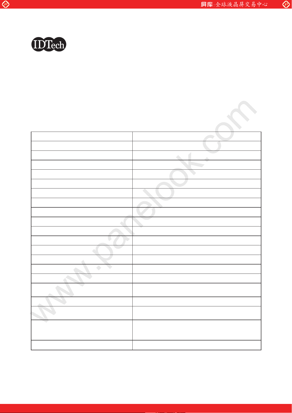
The following items are characteristics summary on the table under 25 degree C condition:
CHARACTERISTICS ITEMS SPECIFICATIONS
Screen Diagonal [mm] 381
www.panelook.com
Pixels H x V 1600(x3) x 1200
Active Area [mm] 304.8(H) x 228.6(V)
Pixel Pitch [mm] 0.1905(per one triad) x 0.1905
Pixel Arrangement R,G,B Vertical Stripe
Weight [grams] 690 Typ., 725 Max.
Physical Size [mm] 317.3(W) x 242.0(H) x 7.2(D) Typ./7.5(D) Max.
Display Mode Normally Black
Display Surface Treatment Anti-Glare
Support Color Native 262K colors (RGB 6-bit data driver)
White Luminance [cd/m2] (center) 200 Typ.
Contrast Ratio 400 : 1 Typ.
Optical Rise Time + Fall Time [msec] 60 Typ., 150 Max.
Nominal Input Voltage VDD [Volt] +3.3 Typ.
Power Consumption [Watt](VDD) 2.9 Typ., 3.8 Max.
Lamp Power Consumption [Watt]
Typical Power Consumption [Watt] 7.4 Typ., 8.8 Max. (W/o inverter loss)
4.5 Typ., (W/o inverter loss)
5.0 Max., (W/o inverter loss)
Electrical Interface
Temperature Range [degree C]
Operating
Storage (Shipping)
CFL Cable Length [mm] 35 Typ
(C) Copyright International Display Technology 2002 All Rights reserved
June 2, 2003 CAS I-914K-AV01
One step solution for LCD / PDP / OLED panel application: Datasheet, inventory and accessory!
8 pairs LVDS (Even/Odd R/G/B Data (6bit),
3s
nc signals, Clock
0 to +50
-20 to +60
5/34
www.panelook.com
Page 6
Global LCD Panel Exchange Center
Customer’s Acceptance Specification
www.panelook.com
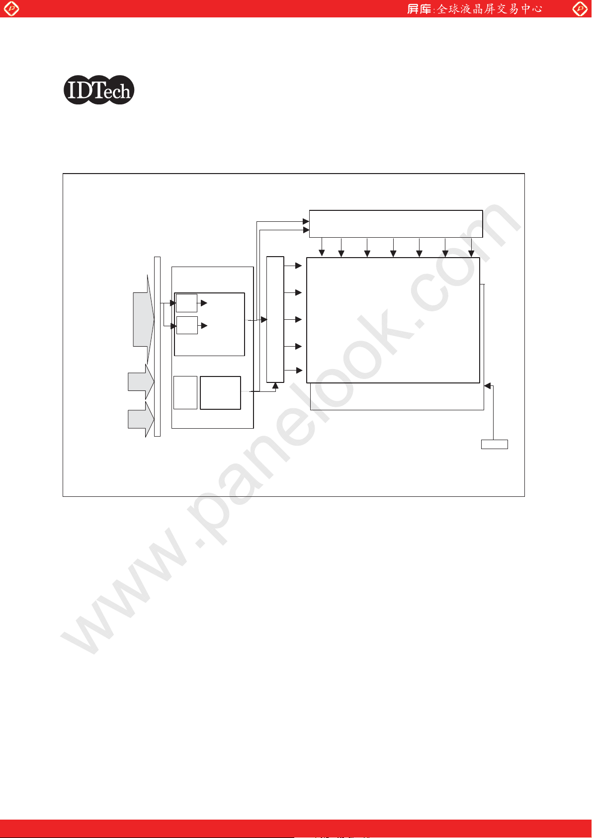
2.2 Functional Block Diagram
The following diagram shows the functional block of this Type 15.0 Color TFT/LCD Module.
The first LVDS port transmits even pixels while the second LVDS port transmits odd pixels.
X-Driver
Y-Driver
< 8 pairs LVDS >
6bit color data
for R/G/B
(even/odd)
DTCLK(even/odd)
DSPTMG
Vsync
Hsync
EEDID
V
EEDID
CLK
EEDID
Data
VDD
EEDID
EVEN
PIXEL
ODD
PIXEL
Dual LVDS
RECEIVER
G/A
Chip
LCD DRIVE
CARD
LCD
Controller
DC-DC
Converter
Ref circuit
TFT ARRAY/CELL
1600(R/G/B) x 1200
Backlight Unit
GND
LCD-DRIVE Connector
Lamp Connector
JST BHSR-02VS-1 (2pin)
JAE FI-XB30S-HF10 (30pin)
(C) Copyright International Display Technology 2002 All Rights reserved
June 2, 2003 CAS I-914K-AV01
6/34
One step solution for LCD / PDP / OLED panel application: Datasheet, inventory and accessory!
www.panelook.com
Page 7
Global LCD Panel Exchange Center
y
Customer’s Acceptance Specification
www.panelook.com
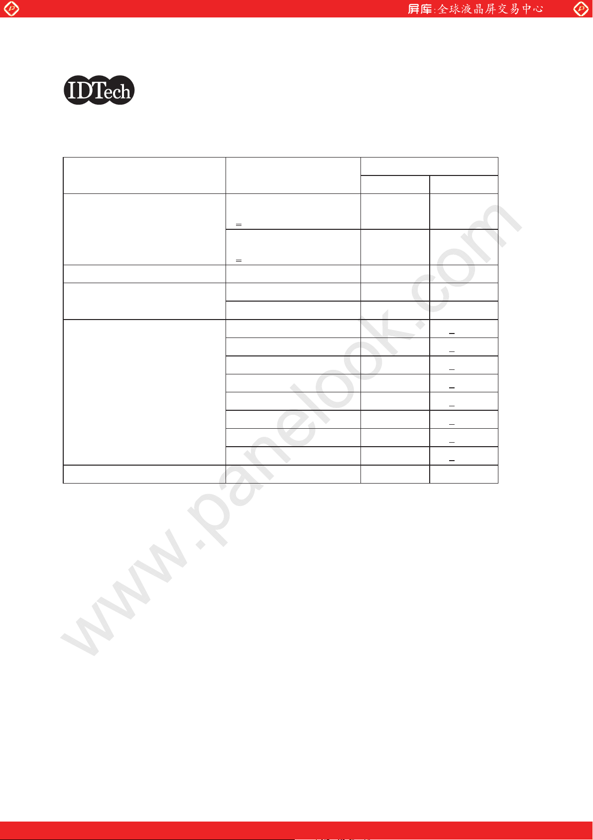
3.0 Absolute Maximum Ratings
Absolute maximum ratings of the module is as follows:
Item S
Logic/LCD Drive Voltage VDD -0.3 +4.0 V
Input Signal Voltage VIN -0.3 VDD+0.3 V
CFL Ignition Voltage Vs - +1,600 Vrms (Note 2)
CFL Current ICFL - +8 mAms
CFL Peak Inrush Current ICFLP - +20 mA
Operating Temperature TOP 0 +50 deg.C (Note 1)
Operating Relative Humidity HOP 8 95 %RH (Note 1)
Storage Temperature TST -20 +60 deg.C (Note 1)
Storage Relative Humidity HST 5 95 %RH (Note 1)
Vibration 1.5 10-200 G Hz
Shock 50 18 G ms Rectangle wave
Note 1: Maximum Wet-Bulb should be 39 degree C and No condensation.
Note 2: Duration : 50msec Max. Ta=0 degree C
mbol Min Max Unit Conditions
(C) Copyright International Display Technology 2002 All Rights reserved
June 2, 2003 CAS I-914K-AV01
One step solution for LCD / PDP / OLED panel application: Datasheet, inventory and accessory!
7/34
www.panelook.com
Page 8
Global LCD Panel Exchange Center
Customer’s Acceptance Specification
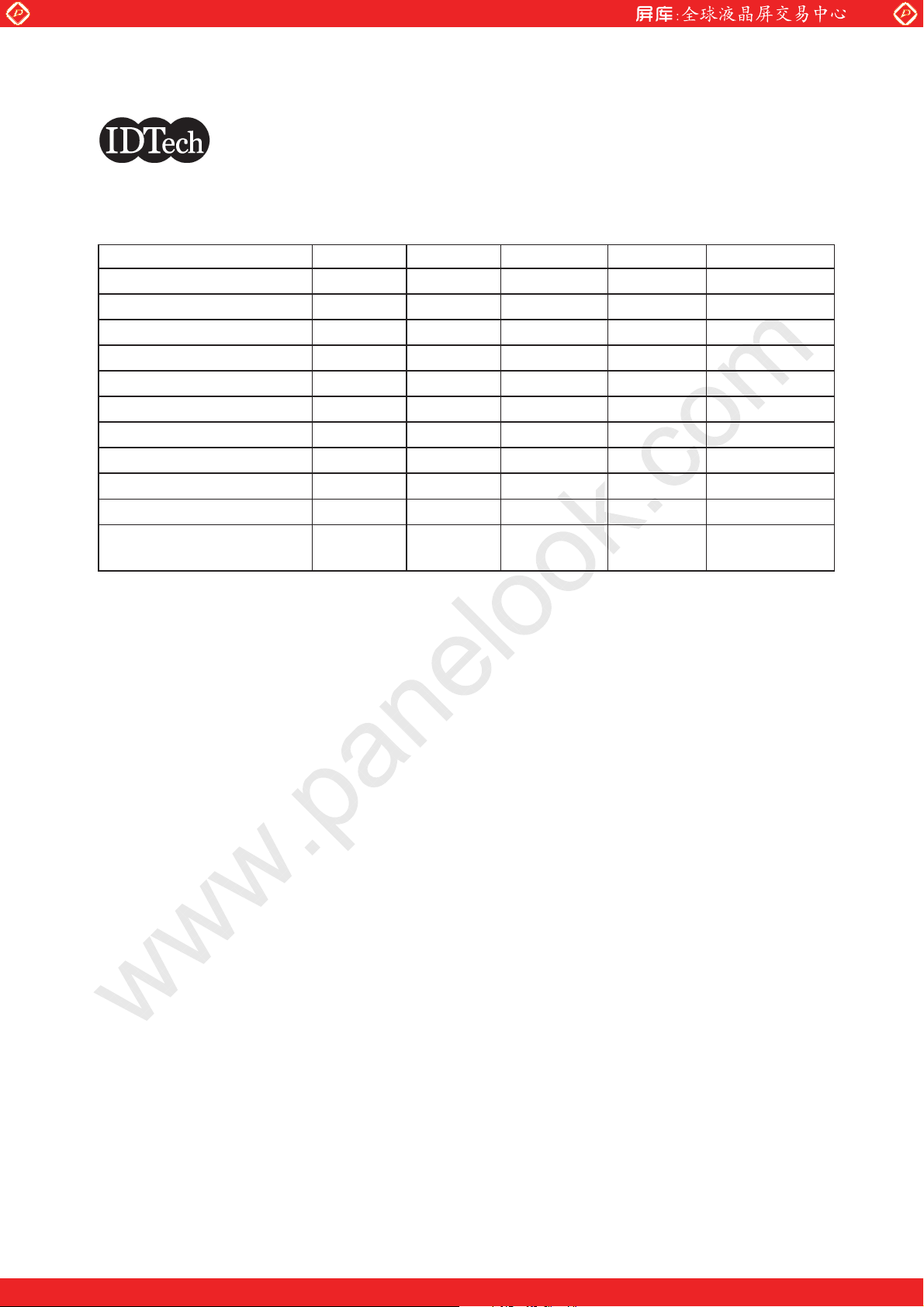
4.0 Optical Characteristics
www.panelook.com
The optical characteristics are measured under stable conditions as follows under 25 degree C condition:
Item Conditions Specification
Typ. Note
Viewing Angle
(Degrees)
K: Contrast Ratio
Contrast ratio 300 -
Response Time Rising 30 -
(ms) Falling 30 -
Color Red x 0.569 +0.030
Chromaticity Red y 0.332 +0.030
(CIE) Green x 0.312 +0.030
Green y 0.544 +0.030
Blue x 0.149 +0.030
Blue y 0.132 +0.030
Horizontal (Right)
K>
10 (Left)
Vertical (Upper)
K>
10 (Lower)
85
85
85
85
-
-
-
-
White x 0.313 +0.030
White y 0.329 +0.030
White Luminance (cd/m2) (center) 200 Typ. 170 Min.
(C) Copyright International Display Technology 2002 All Rights reserved
June 2, 2003 CAS I-914K-AV01
One step solution for LCD / PDP / OLED panel application: Datasheet, inventory and accessory!
8/34
www.panelook.com
Page 9
Global LCD Panel Exchange Center
Customer’s Acceptance Specification
The following is the note for the Optical Characteristics:
www.panelook.com
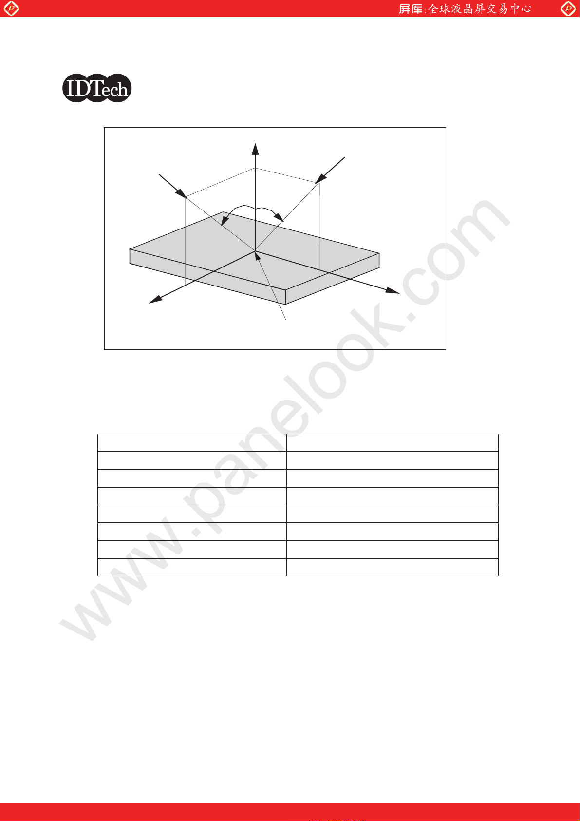
Z
Viewing or M easuring
Direction
+h-v
LEFT
LOW ER
X
CENTER OF LCD
(X=0,Y=0,Z=0)
Viewing or M easuring
Direc tion
UPPER
RIGHT
Y
Chromaticity and White Balance are defined as the C.I.E. 1931 x,y coordinates at the center of LCD.
The Standard Equipment are as shown below table.
Item Standard Equipment
Viewing Angle MCPD-7000 by Ohtsuka Elec
Contrast MCPD-7000 by Ohtsuka Elec
Response Time BM5A by TOPCON OPTICAL Co.,Ltd.
White Luminance MCPD-7000 by Ohtsuka Elec
Luminance Uniformity MCPD-7000 by Ohtsuka Elec
Chromaticity MCPD-7000 by Ohtsuka Elec
White Balance MCPD-7000 by Ohtsuka Elec
The measurement is to be done after 30 minutes of Power-on of BackLight.
Unless otherwise specified, the ambient conditions are as following.
Ambient Temperature : 25 + 2 ( degreeC )
Ambient Humidity : 25 - 85 ( % )
Atmospheric Pressure : 86.0 - 104.0 ( kPa )
(C) Copyright International Display Technology 2002 All Rights reserved
June 2, 2003 CAS I-914K-AV01
9/34
One step solution for LCD / PDP / OLED panel application: Datasheet, inventory and accessory!
www.panelook.com
Page 10
Global LCD Panel Exchange Center
Customer’s Acceptance Specification
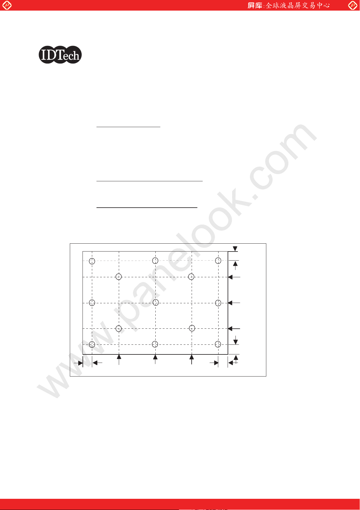
4.1 Luminance Uniformity
When the backlight is on with all pels in the unselected state (white), the luminance uniformity is defined as
follows;
Average luminance is defined as follows.
L1 + L2 + L3 + L4 + L5
Average Luminance =
5
Luminance variation is measured by dividing the maximum luminance values of the 13 or 5 test points by the
minimum luminance of the 13 or 5 test points.
Maximum Luminance 13 Points (L1-L13)
Luminance Uniformity =<1.65
Minimum Luminance 13 Points (L1-L13)
Maximum Luminance 5 Points (L1-L5)
Luminance Uniformity =<1.25
Minimum Luminance 5 Points (L1-L5)
Average luminance and Luminance uniformity test points
www.panelook.com
L6 L7
L9
L11
10mm
L1 L2
L5
L3
L12 L13
400
800
1200
L8
L10
L4
10mm
10mm
300
600
900
10mm
(C) Copyright International Display Technology 2002 All Rights reserved
June 2, 2003 CAS I-914K-AV01
One step solution for LCD / PDP / OLED panel application: Datasheet, inventory and accessory!
10/34
www.panelook.com
Page 11
Global LCD Panel Exchange Center
Customer’s Acceptance Specification
5.0 Signal Interface
5.1 Connectors
Physical interface is described as for the connector on module.
These connectors are capable of accommodating the following signals and will be following components.
Connector Name / Designation For Signal Connector
Manufacturer JAE
Type / Part Number FI-XB30S-HF10
www.panelook.com
Mating Receptacle Manufacture
Mating Receptacle/Part Number
Connector Name / Designation For Lamp Connector
Manufacturer JST
Type / Part Number BHSR-02VS-1
Mating Type / Part Number SM02B-BHSS-1
JAE
FI-X30M
(C) Copyright International Display Technology 2002 All Rights reserved
June 2, 2003 CAS I-914K-AV01
One step solution for LCD / PDP / OLED panel application: Datasheet, inventory and accessory!
11/34
www.panelook.com
Page 12

Global LCD Panel Exchange Center
Customer’s Acceptance Specification
www.panelook.com
5.2 Interface Signal Connector
Pin # Signal Name Pin # Signal Name
1 GND 16 GND
2 VDD 17 ReCLKIN-
3 VDD 18 ReCLKIN+
4 V
(Note 2,3) 19 GND
EEDID
5 Reserved (Note 1) 20 RoIN0-
6 CLK
7 Data
(Note 2,4) 21 RoIN0+
EEDID
(Note 2,4) 22 GND
EEDID
8 ReIN0- 23 RoIN1-
9 ReIN0+ 24 RoIN1+
10 GND 25 GND
11 ReIN1- 26 RoIN2-
12 ReIN1+ 27 RoIN2+
13 GND 28 GND
14 ReIN2- 29 RoCLKIN-
15 ReIN2+ 30 RoCLKIN+
Note:
1. 'Reserved' pins are not allowed to connect any other line.
2. This LCD Module complies with "VESA ENHANCED EXTENDED DISPLAY IDENTIFICATION DATA
STANDARD Release A, Revision 1" and supports "EEDID version 1.3".
This module uses Serial EEPROM BR24C02FV (ROHM) or compatible as a EEDID function.
3. V
(Reference Document: "Enhanced Display Data Channel (E-DDC
4. Both CLK
power source shall be the current limited circuit which has not exceeding 1A.
EEDID
TM
) Proposed Standard", VESA)
line and Data
EEDID
line are pulled-up with 10K ohm resistor to V
EEDID
power source line at
EEDID
LCD panel, respectively.
Voltage levels of all input signals are LVDS compatible (except VDD, EEDID).
Refer to "Signal Electrical Characteristics for LVDS", for voltage levels of all input signals.
(C) Copyright International Display Technology 2002 All Rights reserved
June 2, 2003 CAS I-914K-AV01
One step solution for LCD / PDP / OLED panel application: Datasheet, inventory and accessory!
12/34
www.panelook.com
Page 13

Global LCD Panel Exchange Center
Customer’s Acceptance Specification
www.panelook.com
5.3 Interface Signal Description
The LVDS receiver equipped in this LCD module is compatible with ANSI/TIA/TIA-644 standard.
PIN # SIGNAL NAME Description
1 GND Ground
2 VDD +3.3V Power Supply
3 VDD +3.3V Power Supply
4 V
EEDID 3.3V Power Supply
EEDID
5 Reserved Reserved
6 CLK
7 Data
EEDID Clock
EEDID
EEDID Data
EEDID
8 ReIN0- Negative LVDS differential data input (Even R0-R5, G0)
9 ReIN0+ Positive LVDS differential data input (Even R0-R5, G0)
10 GND Ground
11 ReIN1- Negative LVDS differential data input (Even G1-G5, B0-B1)
12 ReIN1+ Positive LVDS differential data input (Even G1-G5, B0-B1)
13 GND Ground
14 ReIN2- Negative LVDS differential data input (Even B2-B5, HSYNC, VSYNC, DSPTMG)
15 ReIN2+ Positive LVDS differential data input (Even B2-B5, HSYNC, VSYNC, DSPTMG)
16 GND Ground
17 ReCLKIN- Negative LVDS differential clock input (Even)
18 ReCLKIN+ Positive LVDS differential clock input (Even)
19 GND Ground
20 RoIN0- Negative LVDS differential data input (Odd R0-R5, G0)
21 RoIN0+ Positive LVDS differential data input (Odd R0-R5, G0)
22 GND Ground
23 RoIN1- Negative LVDS differential data input (Odd G1-G5, B0-B1)
24 RoIN1+ Positive LVDS differential data input (Odd G1-G5, B0-B1)
25 GND Ground
26 RoIN2- Negative LVDS differential data input (Odd B2-B5)
27 RoIN2+ Positive LVDS differential data input (Odd B2-B5)
28 GND Ground
29 RoCLKIN- Negative LVDS differential clock input (Odd)
30 RoCLKIN+ Positive LVDS differential clock input (Odd)
Note:
Input signals of odd and even clock shall be the same timing.
The module uses a 100ohm resistor between positive and negative data lines of each receiver input.
Even: First Pixel data
Odd : Second Pixel Data
(C) Copyright International Display Technology 2002 All Rights reserved
June 2, 2003 CAS I-914K-AV01
13/34
One step solution for LCD / PDP / OLED panel application: Datasheet, inventory and accessory!
www.panelook.com
Page 14

Global LCD Panel Exchange Center
Customer’s Acceptance Specification
SIGNAL NAME Description
+RED 5 RED Data 5 (MSB)
+RED 4 RED Data 4
+RED 3 RED Data 3
+RED 2 RED Data 2
+RED 1 RED Data 1
+RED 0 RED Data 0 (LSB)
(EVEN/ODD)
Red-pixel Data: Each red pixel's brightness data consists of these 6 bits pixel data.
+GREEN 5 GREEN Data 5 (MSB)
+GREEN 4 GREEN Data 4
+GREEN 3 GREEN Data 3
+GREEN 2 GREEN Data 2
+GREEN 1 GREEN Data 1
+GREEN 0 GREEN Data 0 (LSB)
(EVEN/ODD)
Green-pixel Data: Each green pixel's brightness data consists of these 6 bits pixel data.
+BLUE 5 BLUE Data 5 (MSB)
+BLUE 4 BLUE Data 4
+BLUE 3 BLUE Data 3
+BLUE 2 BLUE Data 2
+BLUE 1 BLUE Data 1
+BLUE 0 BLUE Data 0 (LSB)
(EVEN/ODD)
Blue-pixel Data: Each blue pixel's brightness data consists of these 6 bits pixel data.
-DTCLK Data Clock: The typical frequency is 81MHz.
(EVEN/ODD) The signal is used to strobe the pixel + data and the + DSPTMG
+DSPTMG Display Timing:
When the signal is high, the pixel data shall be valid to be displayed.
VSYNC Vertical Sync: This signal is synchronized with -DTCLK. Both active high/low signals are
acceptable.
HSYNC Horizontal Sync: This signal is synchronized with -DTCLK. Both active high/low signals are
acceptable.
VDD Power Supply
www.panelook.com
GND Ground
V
EEDID Power Supply
EEDID
CLK
Data
Note: Output signals except V
EEDID Clock
EEDID
EEDID Data
EEDID
EEDID
, CLK
EEDID
and Data
from any system shall be Hi-Z state when VDD is off.
EEDID
(C) Copyright International Display Technology 2002 All Rights reserved
June 2, 2003 CAS I-914K-AV01
One step solution for LCD / PDP / OLED panel application: Datasheet, inventory and accessory!
14/34
www.panelook.com
Page 15
Global LCD Panel Exchange Center
Customer’s Acceptance Specification
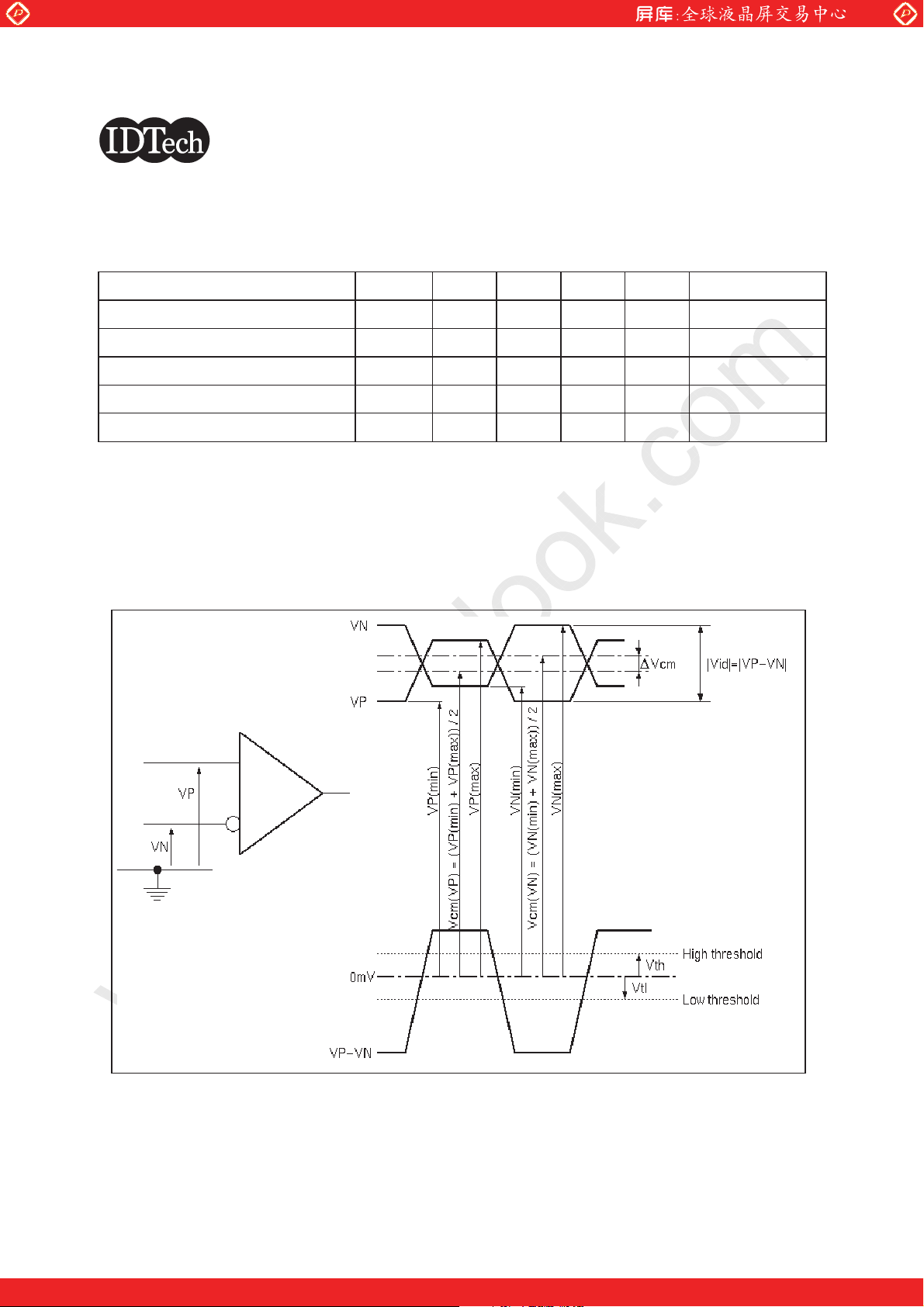
5.4 Interface Signal Electrical Characteristics
5.4.1 Signal Electrical Characteristics for LVDS Receiver
Electrical Characteristics
Parameter Symbol Min Typ Max Unit Conditions
Differential Input High Threshold Vth +100 mV Vcm=+1.2V
Differential Input Low Threshold Vtl -100 mV Vcm=+1.2V
Magnitude Differential Input Voltage |Vid| 100 600 mV
Common Mode Voltage Vcm 1.0 1.2 1.4 V Vth - Vtl = 200mV
Common Mode Voltage Offset Vcm -50 +50 mV Vth - Vtl = 200mV
Note:
Input signals shall be low or Hi-Z state when VDD is off.
All electrical characteristics for LVDS signal are defined and shall be measured at the interface connector
of LCD (see Figure Measurement system).
Voltage Definitions
www.panelook.com
(C) Copyright International Display Technology 2002 All Rights reserved
June 2, 2003 CAS I-914K-AV01
One step solution for LCD / PDP / OLED panel application: Datasheet, inventory and accessory!
15/34
www.panelook.com
Page 16

Global LCD Panel Exchange Center
Customer’s Acceptance Specification
Measurement system
www.panelook.com
(C) Copyright International Display Technology 2002 All Rights reserved
June 2, 2003 CAS I-914K-AV01
One step solution for LCD / PDP / OLED panel application: Datasheet, inventory and accessory!
16/34
www.panelook.com
Page 17

Global LCD Panel Exchange Center
Customer’s Acceptance Specification
Switching Characteristics
Parameter Symbol Min Typ Max Unit Conditions
Clock Frequency fc 53.0 81.0 83.0 MHz
Cycle Time tc 12.0 12.3 18.9 ns
Data Setup Time (Note 1) Tsu 500 ps
Data Hold Time (Note 2) Thd 500 ps
Cycle-to-cycle jitter (Note 3) tCCJ -150 +150 ps fc = 81MHz
Cycle Modulation Rate (Note 4) tCJavg 20 ps/clk fc = 81MHz
Note 1: All values are at VDD=3.3V, Ta=25 degree C.
Note 2: See figure "Timing Definition" and "Timing Definition (detail A)" for definition.
Note 3: Jitter is the magnitude of the change in input clock period.
Note 4: This specification defines maximum average cycle modulation rate in peak-to-peak transition within
any 100 clock cycles. This specification is applied only if input clock peak jitter within any 100 clock
cycles is greater than 300ps.
Timing Definition (Even)
www.panelook.com
fc = 81MHz, tCCJ < 50ps,
Vth-Vtl = 200mV,
Vcm = 1.2V, Vcm = 0
(C) Copyright International Display Technology 2002 All Rights reserved
June 2, 2003 CAS I-914K-AV01
One step solution for LCD / PDP / OLED panel application: Datasheet, inventory and accessory!
17/34
www.panelook.com
Page 18
Global LCD Panel Exchange Center
Customer’s Acceptance Specification
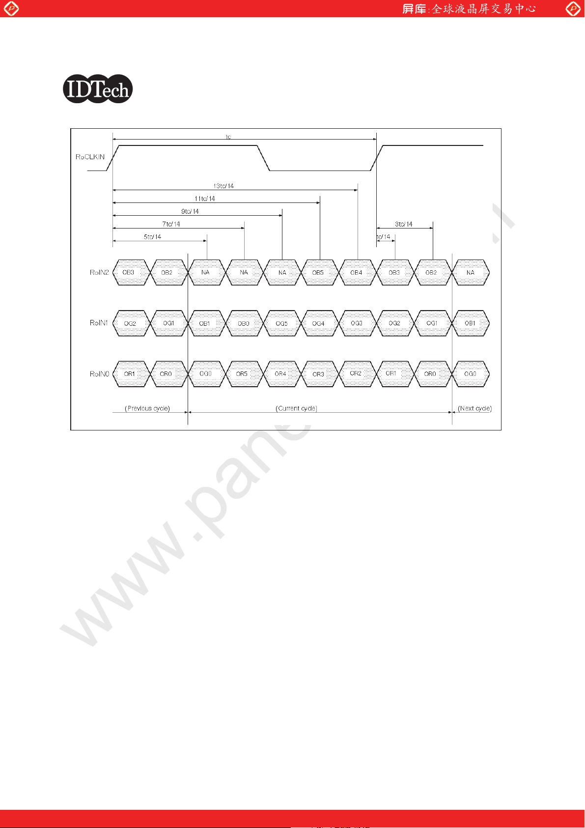
Timing Definition (Odd)
www.panelook.com
(C) Copyright International Display Technology 2002 All Rights reserved
June 2, 2003 CAS I-914K-AV01
One step solution for LCD / PDP / OLED panel application: Datasheet, inventory and accessory!
18/34
www.panelook.com
Page 19

Global LCD Panel Exchange Center
Customer’s Acceptance Specification
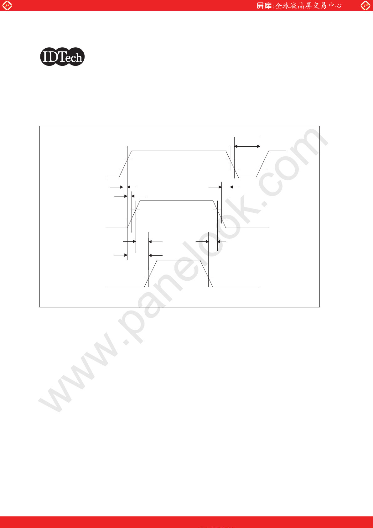
Timing Definition (detail A)
www.panelook.com
Note: Tsu and Thd are internal data sampling window of receiver. Trskm is the system skew margin; i.e.,
the sum of cable skew, source clock jitter, and other inter-symbol interference, shall be less than Trskm.
(C) Copyright International Display Technology 2002 All Rights reserved
June 2, 2003 CAS I-914K-AV01
19/34
One step solution for LCD / PDP / OLED panel application: Datasheet, inventory and accessory!
www.panelook.com
Page 20

Global LCD Panel Exchange Center
Customer’s Acceptance Specification
5.4.2 LVDS Receiver Internal Circuit
Below figure shows the internal block diagram of the LVDS receiver.
5.4.3 Recommended Guidelines for Motherboard PCB Design and Cable Selection
www.panelook.com
Following the suggestions below will help to achieve optimal results.
Use controlled impedance media for LVDS signals. They should have a matched differential impedance of
100ohm.
Match electrical lengths between traces to minimize signal skew.
Isolate TTL signals from LVDS signals.
For cables, twisted pair, twinax, or flex circuit with close coupled differential traces are recommended.
5.5 Signal for Lamp Connector
Pin # Signal Name
1 Lamp High Voltage
2 Lamp Low Voltage
(C) Copyright International Display Technology 2002 All Rights reserved
June 2, 2003 CAS I-914K-AV01
20/34
One step solution for LCD / PDP / OLED panel application: Datasheet, inventory and accessory!
www.panelook.com
Page 21

Global LCD Panel Exchange Center
Customer’s Acceptance Specification
6.0 Pixel format image
Following figure shows the relationship of the input signals and LCD pixel format image. Even and odd pair of
RGB data are sampled at a time.
Even Odd Even Odd
0 1 1599
1st Line
1200th Line
RGB RGB
RGB RGB
www.panelook.com
1598
RGB RGB
RGB RGB
(C) Copyright International Display Technology 2002 All Rights reserved
June 2, 2003 CAS I-914K-AV01
One step solution for LCD / PDP / OLED panel application: Datasheet, inventory and accessory!
21/34
www.panelook.com
Page 22

Global LCD Panel Exchange Center
Customer’s Acceptance Specification
7.0 Parameter guide line for CFL Inverter
PARAMETER MIN DP-1 MAX UNITS CONDITION
White Luminance - 200 - cd/m2(Ta=25 deg.C)
CFL current (ICFL) 3.0 7.65 8 mArms (Ta=25 deg.C)
CFL Frequency (FCFL) 40 60 KHz (Ta=25 deg.C) (Note 1)
CFL Ignition Voltage (Vs) 1,500 - - Vrms (Ta= 0 deg.C) (Note 3)
CFL Voltage (Reference)(VCFL) - 590 - Vrms (Ta=25 deg.C) (Note 2)
CFL Power consumption (PCFL) - 4.5 5 W (Ta=25 deg.C) (Note 2)
www.panelook.com
Note 1: CFL discharge frequency should be carefully determined to avoid interference between inverter and
TFT LCD.
Note 2: Calculated value for reference (ICFL x VCFL = PCFL).
Note 3: CFL inverter should be able to give out a power that has a generating capacity of over 1,500 voltage.
Lamp units need 1,500 voltage minimum for ignition.
Note 4: DP-1 (Design Point-1) is recommended Design Point.
*1 All of characteristics listed are measured under the condition using the Test inverter.
*2 In case of using an inverter other than listed, it is recommended to check the inverter carefully.
Sometimes, interfering noise stripes appear on the screen, and substandard luminance or flicker at
low power may happen.
*3 In designing an inverter, it is suggested to check safety circuit very carefully.
Impedance of CFL, for instance, becomes more than 1 [M ohm] when CFL is damaged.
*4 Generally, CFL has some amount of delay time after applying kick-off voltage.
It is recommended to keep on applying kick-off voltage for 1 [Sec] until discharge.
*5 Reducing CFL current increases CFL discharge voltage and generally increases CFL discharge
frequency. So all the parameters of an inverter should be carefully designed so as not to produce
too much leakage current from high-voltage output of the inverter.
*6 It should be employed the inverter which has 'Duty Dimming', if ICFL is less than 4[mA].
(C) Copyright International Display Technology 2002 All Rights reserved
June 2, 2003 CAS I-914K-AV01
One step solution for LCD / PDP / OLED panel application: Datasheet, inventory and accessory!
22/34
www.panelook.com
Page 23

Global LCD Panel Exchange Center
Customer’s Acceptance Specification
www.panelook.com
The following chart is Luminance versus Lamp Power for your reference.
(C) Copyright International Display Technology 2002 All Rights reserved
June 2, 2003 CAS I-914K-AV01
One step solution for LCD / PDP / OLED panel application: Datasheet, inventory and accessory!
23/34
www.panelook.com
Page 24

Global LCD Panel Exchange Center
Customer’s Acceptance Specification
8.0 Interface Timings
Basically, interface timings described here is not actual input timing of LCD module but output timing of
SN75LVDS86 (Texas Instruments) or equivalent.
8.1 Timing Characteristics
Signal Item Symbol MIN. TYP. MAX. Unit
www.panelook.com
Fdck 53.0 81.0 83.0 [MHz]DTCLK Freqency
Tck 12.0 12.3 18.8 [ns]
Fv - 60.0 - [Hz] +V-Sync Frame Rate
Tv - 16.67 - [ms]
Nv 1208 1250 2046 [lines]
Tva 13.33 40.0 839.8 [us]
V-Back Porch Nvb 6 46 125 [lines]
V-Front Porch Nvf 1 1 125 [lines]
+DSPTMG V-Line m 1200 [lines]
Nh 1024 1080 2046 [Tck]
Tha 1.185 [usec]
H-Back Porch Thb 8 152 511 [Tck]
H-Front Porch Thf 8 32 [Tck]
+DSPTMG Display Thd 9.877 [usec]
+DATA Data Even/Odd n 1600 [dots]
Note: Both positive Hsync and positive Vsync polarity is recommended.
Disp Timing Period (Th, Nh) must be constant by each every line.
If Disp timing are not constant due to Spread Spectrum, the following expression has to be satisfied.
DeltaDT x Tvblk < 300 [Tck]
DTmax : Disp Timing Period MAX [Tck]
DTmin : Disp Timing Period MIN [Tck]
DeltaDT = DTmax - DTmin
Tvblk : V Blanking [lines]
Tck : DTCLK
(C) Copyright International Display Technology 2002 All Rights reserved
June 2, 2003 CAS I-914K-AV01
V-Active Level
Nva 1 3 63 [lines]
Fh - 75.0 - [KHz]+H-Sync Scan Rate
Th - 13.33 - [usec]
H-Active Level
Tha 8 96 255 [Tck]
24/34
One step solution for LCD / PDP / OLED panel application: Datasheet, inventory and accessory!
www.panelook.com
Page 25

Global LCD Panel Exchange Center
Customer’s Acceptance Specification
8.2 Timing Definition
Vertical Timing
Support mode Tvblk
Vertical
Blanking
1600 x 1200 at 60Hz
(H line rate : 13.3 us)
0.667 ms
(50 lines)
DSP TMG
Tvf
m
Active Field
16.000 ms
(1200 lines)
Tvbl k
Tva
www.panelook.com
Tvf VSYNC
Front Porch
0.013 ms
(1 line)
Tv
Tvb
Tv,Nv
Frame Time
16.667 ms
(1250 lines)
m
Tva VSYNC
Width
0.040 ms
(3 lines)
Tvb VSYNC
Back Porch
0.613 ms
(46 lines)
+VSYNC
Horizontal Timing
Support mode Thblk
1600 x 1200
Dotclock : 162.000 MHz
(81.000MHz x2)
DSPTMG
-H S Y N C
+HSYN C
VIDEO (Even)
VIDEO (Even)
Horizontal
Blanking
3.457 us
(560 dots)
Thf
Thd
Active Field
Thf
HSYNC
Th,Nh
H Line Time
Front Porch
9.877 us
(1600 dots)
Thblk Thd
Tha
Thb
0.395 us
(64 dots)
Th
Tck
02
13.333 us
(2160 dots)
4
Tha
HSYNC
Width
1.185 us
(192 dots)
n-4 n-2
Thb
HSYNC
Back Porch
1.877 us
(304 dots)
VIDEO (Odd)
VIDEO (Odd)
DTCLK
13
5
n-3
n-1
(C) Copyright International Display Technology 2002 All Rights reserved
June 2, 2003 CAS I-914K-AV01
One step solution for LCD / PDP / OLED panel application: Datasheet, inventory and accessory!
25/34
www.panelook.com
Page 26
Global LCD Panel Exchange Center
pp
pp
Customer’s Acceptance Specification
www.panelook.com
9.0 Power Specifications
SYMBOL PARAMETER Min Typ Max UNITS CONDITION
VDD Logic/LCD Drive Voltage 3.0 3.3 3.6 [V]
PDD VDD Power 3.8 [W]
PDD VDD Power 2.9 [W]
IDD VDD Current 1.25 [A]
IDD VDD Current 0.88 [A]
VDDrp
VDDns
MAX. Pattern: Sub-Pixel Checker.
(C) Copyright International Display Technology 2002 All Rights reserved
June 2, 2003 CAS I-914K-AV01
Allowable Logic/LCD
Drive Ri
Allowable Logic/LCD
Drive Ri
le Voltage
le Noise
Load Capacitance
68 uF
MAX. Pattern,
VDD=3.6[V]
All White Pattern,
VDD=3.3[V]
MAX Pattern,
VDD=3.0[V]
All White Pattern,
VDD=3.3[V]
100 [mVp-p]
100 [mVp-p]
26/34
One step solution for LCD / PDP / OLED panel application: Datasheet, inventory and accessory!
www.panelook.com
Page 27
Global LCD Panel Exchange Center
Customer’s Acceptance Specification
10.0 Power ON/OFF Sequence
VDD power and lamp on/off sequence is as follows. Interface signals are also shown in the chart. Signals from
www.panelook.com
any system shall be Hi-Z state or low level when VDD is off.
VDD
10%
0 V
Signals
0 V
(Recommended).
Lamp
90%
10ms max.
0 min.
90% 90%
10% 10%
100ms min.
180ms min.
On
150ms min.
90%
10% 10%
0 min.
20ms min.
(C) Copyright International Display Technology 2002 All Rights reserved
June 2, 2003 CAS I-914K-AV01
27/34
One step solution for LCD / PDP / OLED panel application: Datasheet, inventory and accessory!
www.panelook.com
Page 28
Global LCD Panel Exchange Center
Customer’s Acceptance Specification
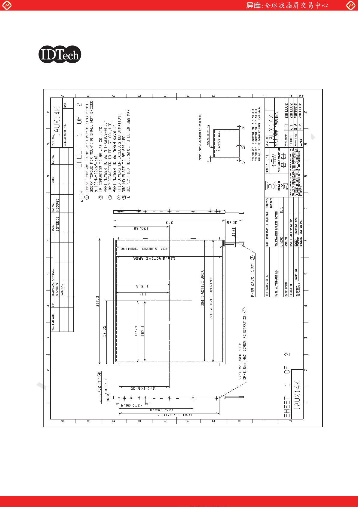
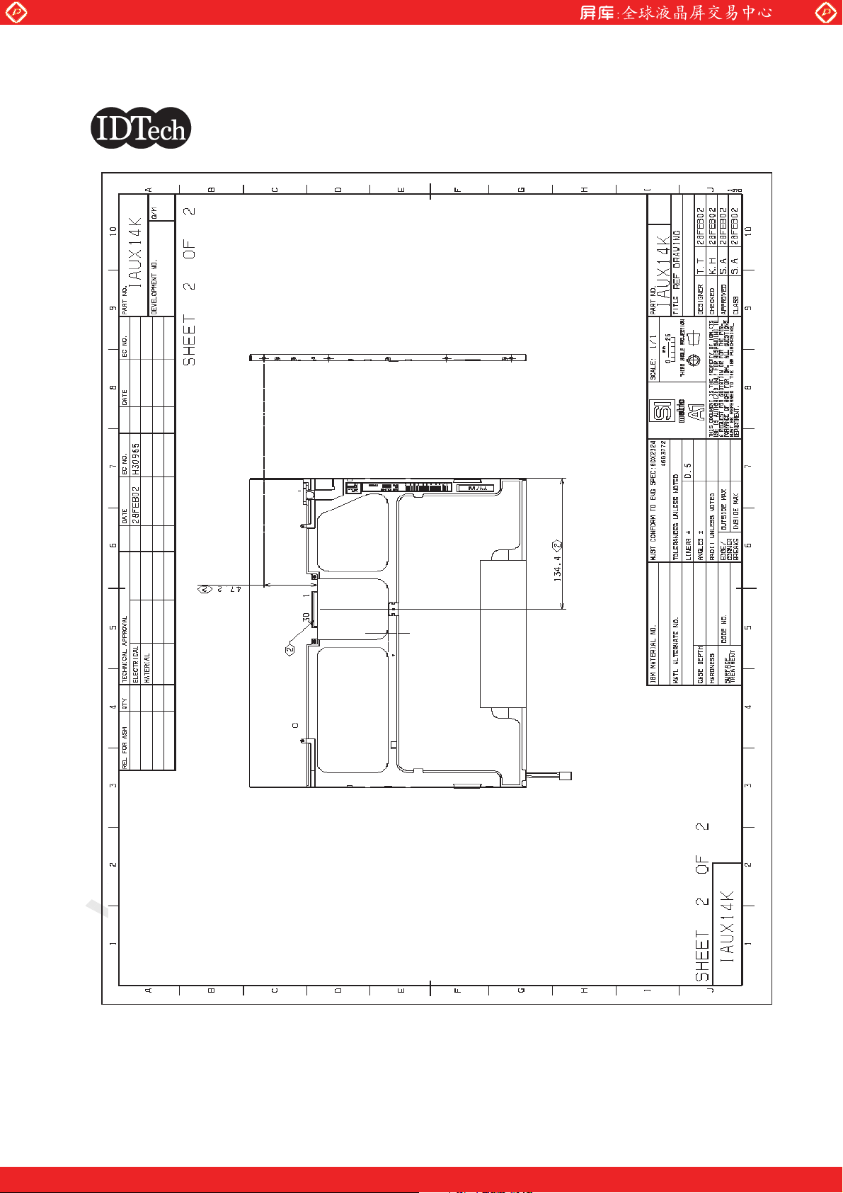
11.0 Mechanical Characteristics
www.panelook.com
(C) Copyright International Display Technology 2002 All Rights reserved
June 2, 2003 CAS I-914K-AV01
One step solution for LCD / PDP / OLED panel application: Datasheet, inventory and accessory!
28/34
www.panelook.com
Page 29
Global LCD Panel Exchange Center
Customer’s Acceptance Specification
www.panelook.com
(C) Copyright International Display Technology 2002 All Rights reserved
June 2, 2003 CAS I-914K-AV01
One step solution for LCD / PDP / OLED panel application: Datasheet, inventory and accessory!
29/34
www.panelook.com
Page 30
Global LCD Panel Exchange Center
Customer’s Acceptance Specification
12.0 National Test Lab Requirement
The display module is satisfied all requirements for compliance to
www.panelook.com
UL60950 3rd. Ed. U.S.A. Information Technology Equipment
13.0 Qualifications and CFL Life
This Quality Specification is for the UXGA TFT-LCD module IAUX14K supplied from International Display
Technology to the customer.
Please pay attention the following items, when this LCD Module is checked in your inspection.
1. You should consider the LCD Module to mount that uneven force is not applied to this LCD Module.
2. Do not push and put a label on the rear side that is located backlight.
3. Do not joggle the LCD Module, there will be some ripple on the screen.
4. Display qualifications depend on the power on time.
The visual screen quality is applied the state since 30 seconds after power on.
13.1 Visual Screen Quality
The following Table describes the visual screen quality of the general TFT-LCD module at power-off.
Polarizer Scratch/Bubble Size (mm) Allowable maximum counts
Elliptical defects d < 0.15 Disregarded
0.15 < d < 0.30 4
0.30 < d 0
Linear defects w < 0.05 Disregarded
0.05 < w < 0.07 and I < 2.0 4
0.07 < w or 2.0 < l 0
d : diameter
longaxis + shortaxis
d=
2
w : line width
l : line length
(C) Copyright International Display Technology 2002 All Rights reserved
June 2, 2003 CAS I-914K-AV01
30/34
One step solution for LCD / PDP / OLED panel application: Datasheet, inventory and accessory!
www.panelook.com
Page 31
Global LCD Panel Exchange Center
Customer’s Acceptance Specification
www.panelook.com
13.2 Line Defect
No visible line defect is allowed in entire screen.
A Line Defect is defined as a horizontal and vertical apparent line, visible through 5% ND-filter, that differs from
adjacent lines at any gray raster pattern.
13.3 Bright and Black Dots
The following Table describes the specification of bright and black dots in the visual screen quality of the
TFT-LCD module at power-ON.
Items Specification
Any Bright Dots
Bright and Black Dots (total)
Definitions:
1. A Bright Dot is a lit subpixel under all black.
2. A Black Dot is an unlit subpixel under maximum brightness single color pattern
(Red, Green, Blue) or full white.
Basic Conditions:
Viewing Distance 350 to 500 mm
Ambient Illumination 300 to 700 lux
Ambient Temperature 20 to 25 degreeC
13.4 CFL Life
CFL Life Time 10,000 Hours condition 25 degree C and 7.65mArms
The assumed CFL Life will be until the luminance becomes 50% of it's initial value of the panel.
6 Max
15 Max
(C) Copyright International Display Technology 2002 All Rights reserved
June 2, 2003 CAS I-914K-AV01
One step solution for LCD / PDP / OLED panel application: Datasheet, inventory and accessory!
31/34
www.panelook.com
Page 32

Global LCD Panel Exchange Center
Customer’s Acceptance Specification
14.0 Packaging Specification
The packaging of the LCD meets 75 cm drop test.
The following is the drawing of the package.
www.panelook.com
(C) Copyright International Display Technology 2002 All Rights reserved
June 2, 2003 CAS I-914K-AV01
One step solution for LCD / PDP / OLED panel application: Datasheet, inventory and accessory!
32/34
www.panelook.com
Page 33

Global LCD Panel Exchange Center
Customer’s Acceptance Specification
15.0 Label
There are labels on the rear side of the Module.
Serial Number Label
BARCODE CHARACTER AREA
www.panelook.com
11S ppppppp Z 1Z hhh SSSSSS
1
1
11S = FIXED
Starting identifier which
is common to component
level serial numbers.
2
Seven digit IBM part number
Assigned by the IBM laboratory
releasing the part
3
Z = FIXED
Automatically given
when using the
11S-Z format
2 3 4 5
1Z = FIXED
4
Location code
5
hhh = Header code
(Depend on EC Level and
Manufacturing Location)
SSSSSS = Serial Number
6
6
Date Label
YY and WW of the Week Code stand for the Year and the Week of the Year of manufacturing of the Module
respectively.
(C) Copyright International Display Technology 2002 All Rights reserved
June 2, 2003 CAS I-914K-AV01
One step solution for LCD / PDP / OLED panel application: Datasheet, inventory and accessory!
33/34
www.panelook.com
Page 34

Global LCD Panel Exchange Center
Customer’s Acceptance Specification
www.panelook.com
UL Label
****** End Of Page ******
(C) Copyright International Display Technology 2002 All Rights reserved
June 2, 2003 CAS I-914K-AV01
One step solution for LCD / PDP / OLED panel application: Datasheet, inventory and accessory!
34/34
www.panelook.com
 Loading...