

Page 1
Global LCD Panel Exchange Center
Engineering Specification
www.panelook.com
Engineering Specification
Type 15.0 QXGA Color TFT/LCD Module
Model Name:IAQX10M
Document Control Number : OEM I-910M-03
Note:Specification is subject to change without notice. Consequently it is better to contact to
International Display Technology before proceeding with the design
of your product incorporating this module.
Sales Support
International Display Technology
(C) Copyright International Display Technology 2001, 2002 All Rights reserved.
June 17,2002 OEM I-910M-03 1/30
One step solution for LCD / PDP / OLED panel application: Datasheet, inventory and accessory!
www.panelook.com
Page 2

Global LCD Panel Exchange Center
Engineering Specification
i Contents
i Contents
ii Record of Revision
1.0 Handling Precautions
2.0 General Description
2.1 Characteristics
2.2 Functional Block Diagram
3.0 Absolute Maximum Ratings
4.0 Optical Characteristics
5.0 Signal Interface
5.1 Connectors
5.2 Interface Signal Connector
5.3 Interface Signal Description
5.4 Interface Signal Electrical Characteristics
5.4.1 Signal Electrical Characteristics for LVDS Receiver
5.4.2 LVDS Receiver Internal Circuit
5.4.3 Recommended Guidelines for Motherboard PCB Design and Cable Selection
5.5 Signal for Lamp connector
6.0 Pixel format image
7.0 Parameter guide line for CFL Inverter
8.0 Interface Timings
8.1 Timing Characteristics
8.2 Timing Definition
9.0 Power Consumption
10.0 Power ON/OFF Sequence
11.0 Mechanical Characteristics
12.0 National Test Lab Requirement
www.panelook.com
(C) Copyright International Display Technology 2001, 2002 All Rights reserved.
June 17,2002 OEM I-910M-03 2/30
One step solution for LCD / PDP / OLED panel application: Datasheet, inventory and accessory!
www.panelook.com
Page 3
Global LCD Panel Exchange Center
Engineering Specification
ii Record of Revision
www.panelook.com
Date
Revision
OEM I-910M-02March 12,2002
AllOEM I-910M-01November 13,2001
4
6
7
9
11
12,13
14-18
19
22
26
28,29
SummaryPageDocument
First Edition for customer.
Based on Internal Spec. EC H31229 as of November
9,2001.
Based on Internal Spec. EC H31230 as of February
20,2002.
To update Handling Precautions.
To update following items.
Weight
Physical Size
White Luminance
Power Consumption (VDD Line)
Lamp Power Consumption
To add Note for Temperature Range.
To eliminate Optional part in the diagram.
To update following items.
Max. value of Response Time
Color Chromaticity
White Luminance (ICFL)
To update Interface Signal Connector.
To update Interface Signal Description.
To update Signal Electrical Characteristics for LVDS
Receiver.
To add Recommended Guidelines for Motherboard PCB
Design and Cable Selection.
To update Parameter guide line for CFL Inverter.
To update Typ. value of Power Consumption.
To update Reference Drawings.
OEM I-910M-03June 17,2002
4
13
15
22
24
(C) Copyright International Display Technology 2001, 2002 All Rights reserved.
June 17,2002 OEM I-910M-03 3/30
Based on Internal Spec. EC H31231 as of May 10,2002.
To update Handling Precautions.
To update Electrical Characteristics.
To update Switching Characteristics.
To delete 5.0[mA] lamp condition.
To update Timing Characteristics.
One step solution for LCD / PDP / OLED panel application: Datasheet, inventory and accessory!
www.panelook.com
Page 4
Global LCD Panel Exchange Center
Engineering Specification
1.0 Handling Precautions
O If any signals or power lines deviate from the power on/off sequence, it may cause shorten the life of the
LCD module.
O The LCD panel and the CFL are made of glass and may break or crack if dropped on a hard surface, so
please handle them with care.
O CMOS-ICs are included in the LCD panel. They should be handled with care, to prevent electrostatic
discharge.
O Do not press the reflector sheet at the back of the LCD module to any directions.
O Do not stick the adhesive tape on the reflector sheet at the back of the LCD module.
O Please handle care when mount in the system cover. Mechanical damage for lamp cable and for lamp
connector may cause safety problems.
O Small amount of materials having no flammability grade is used in the LCD module. The LCD module
should be supplied by power complied with requirements of Limited Power Source (2.5, IEC60950 or
UL60950), or be applied exemption conditions of flammability requirements (4.7.3.4, IEC60950 or
UL60950) in an end product.
O The LCD module is designed so that the CFL in it is supplied by Limited Current Circuit (2.4, IEC60950 or
UL1950).
O The fluorescent lamp in the liquid crystal display(LCD) contains mercury. Do not put it in trash that is
disposed of in landfills. Dispose of it as required by local ordinances or regulations.
O Never apply detergent or other liquid directly to the screen.
O Wipe off water drop immediately. Long contact with water may cause discoloration or spots.
O When the panel surface is soiled, wipe it with absorbent cotton or other soft cloth; do not use solvents or
abrasives.
O Do not touch the front screen surface in your system, even bezel.
O
The information contained herein is presented only as a guide for the applications of our
products. No responsibility is assumed by International Display Technology for any
infringements of patents or other right of the third partied which may result from its use. No
license is granted by implication or otherwise under any patent or patent rights of International
Display Technology or others.
O
The information contained herein may be changed without prior notice. It is therefore
advisable to contact International Display Technology before proceeding with the design of
equipment incorporationg this product.
www.panelook.com
(C) Copyright International Display Technology 2001, 2002 All Rights reserved.
June 17,2002 OEM I-910M-03 4/30
One step solution for LCD / PDP / OLED panel application: Datasheet, inventory and accessory!
www.panelook.com
Page 5
Global LCD Panel Exchange Center
Engineering Specification
2.0 General Description
This specification applies to the Type 15.0 Color TFT/LCD Module 'IAQX10M'.
This module is designed for a display unit of a monitor application.
The screen format and electrical interface are intended to support the QXGA(2048(H) x 1536(V)) screen.
Support color is native 262K colors(RGB 6-bit data driver).
All input signals are LVDS(Low Voltage Differential Signaling) interface compatible.
This module does not contain an inverter card for backlight.
2.1 Characteristics
The following items are characteristics summary on the table under 25 degree C condition:
www.panelook.com
SPECIFICATIONSCHARACTERISTICS ITEMS
2
White Luminance [cd/m
ICFL=7.0mA
Optical Rise Time + Fall Time [msec]
]
380Screen Diagonal [mm]
2048(x3) x 1536Pixels H x V
304.1(H) x 228.1(V)Active Area [mm]
0.1485(per one triad) x 0.1485Pixel Pitch [mm]
R,G,B Vertical StripePixel Arrangement
1065 Typ., 1100 Max.Weight [grams]
326.0(W) x 244.5(H) x 13.0(D) Typ./13.3(D) Max. Physical Size [mm]
Normally BlackDisplay Mode
Native 262K colors(RGB 6-bit data driver)Support Color
200 Typ. (center)
180 Typ. (5 points average)
400 : 1 Typ. Contrast Ratio
60 Typ.
+3.3 Typ.Nominal Input Voltage VDD [Volt]
4.1 Typ., 5.2 Max.Power Consumption [Watt](VDD Line)
Lamp Power Consumption [Watt]
ICFL=7.0mA
Temperature Range [degree C]
Operating
Storage (Shipping)
Note : Max. Operating Temperature 50 degree C in the Spec means the temperature measured for the
point of the front surface of the LCD glass cell.
(C) Copyright International Display Technology 2001, 2002 All Rights reserved.
June 17,2002 OEM I-910M-03 5/30
8.6 Typ. (W/o inverter loss)
8 pairs LVDS(Even/Odd R/G/B Data(6bit), 3sync signals, Clock)Electrical Interface
0 to +50 (Note)
-20 to +60
One step solution for LCD / PDP / OLED panel application: Datasheet, inventory and accessory!
www.panelook.com
Page 6

Global LCD Panel Exchange Center
Engineering Specification
2.2 Functional Block Diagram
The following diagram shows the functional block of this Type 15.0 Color TFT/LCD Module.
The first LVDS port
transmits even pixels while the second LVDS port transmits odd pixels.
www.panelook.com
X-Driver
Y-Driver
< 8 pairs LVDS >
6bit color data
for R/G/B
(even/odd)
DTCLK(even/odd)
DSPTMG
Vsync
Hsync
VDD
GND
LCD-DRIVE Connector
JAE FI-XB30S-HF10 (30pin)
EVEN
PIXEL
ODD
PIXEL
Dual LVDS
RECEIVER
G/A
LCD DRIVE
CARD
LCD
Controller
DC-DC
Converter
Ref circuit
TFT ARRAY/CELL
2048(R/G/B) x 1536
Backlight Unit
Lamp Connectors
JST BHSR-02VS-1 (2pin) x 2
(C) Copyright International Display Technology 2001, 2002 All Rights reserved.
June 17,2002 OEM I-910M-03 6/30
One step solution for LCD / PDP / OLED panel application: Datasheet, inventory and accessory!
www.panelook.com
Page 7
Global LCD Panel Exchange Center
y
Engineering Specification
3.0 Absolute Maximum Ratings
Absolute maximum ratings of the module is as follows :
www.panelook.com
mbol Item
Conditions Unit Max MinS
V+4.0-0.3VDDLogic/LCD Drive Voltage
V+2.6-0.3-Input Voltage on FlatLink pins
VVDD+0.3-0.3VINInput Signal Voltage on all other pins
Vrms+1,600-VsCFL Ignition Voltage
mAms+8.5-ICFLCFL Current
mA+20-ICFLPCFL Peak Inrush Current
deg.C+500TOPOperating Temperature
%RH958HOPOperating Relative Humidity
deg.C+60-20TSTStorage Temperature
%RH955HSTStorage Relative Humidity
G Hz1.5 10-200Vibration
(Note 2)
(Note 1)
(Note 1)
(Note 1)
(Note 1)
Rectangle waveG ms50 18Shock
Note 1 : Maximum Wet-Bulb should be 39 degree C and No condensation.
Note 2 : Duration : 50msec Max. Ta=0 degree C
(C) Copyright International Display Technology 2001, 2002 All Rights reserved.
June 17,2002 OEM I-910M-03 7/30
One step solution for LCD / PDP / OLED panel application: Datasheet, inventory and accessory!
www.panelook.com
Page 8

Global LCD Panel Exchange Center
Engineering Specification
4.0 Optical Characteristics
The optical characteristics are measured under stable conditions as follows under 25 degree C condition:
Viewing Angle
(Degrees)
2
White Luminance (cd/m
ICFL 7.0 mA
)
www.panelook.com
Horizontal (Right)
K}10 (Left)
Vertical (Upper)
K}10 (Lower)K:Contrast Ratio
SpecificationConditionsItem
85
85
85
85
200 Typ.
(Center)
180 Typ.
(5 points average)
NoteTyp.
-
-
-
-
-400Contrast ratio
60 Max.30RisingResponse Time
60 Max.30Falling(ms)
-0.569Red xColor
-0.332Red yChromaticity
-0.312Green x(CIE)
-0.544Green y
-0.149Blue x
-0.132Blue y
-0.313 White x
-0.329 White y
(C) Copyright International Display Technology 2001, 2002 All Rights reserved.
June 17,2002 OEM I-910M-03 8/30
One step solution for LCD / PDP / OLED panel application: Datasheet, inventory and accessory!
www.panelook.com
Page 9

Global LCD Panel Exchange Center
Engineering Specification
5.0 Signal Interface
5.1 Connectors
Physical interface is described as for the connector on module.
These connectors are capable of accommodating the following signals and will be following components.
www.panelook.com
Connector Name / Designation
Manufacturer
Type / Part Number
Mating Receptacle Manufacture
Connector Name / Designation
Manufacturer
Type / Part Number
For Signal Connector
JAE
FI-XB30S-HF10
JAE
FI-X30MMating Receptacle/Part Number
For Lamp Connector
JST
BHSR-02VS-1
SM02B-BHSS-1Mating Type / Part Number
(C) Copyright International Display Technology 2001, 2002 All Rights reserved.
June 17,2002 OEM I-910M-03 9/30
One step solution for LCD / PDP / OLED panel application: Datasheet, inventory and accessory!
www.panelook.com
Page 10

Global LCD Panel Exchange Center
Engineering Specification
5.2 Interface Signal Connector
Signal Connector Pin Assignment
www.panelook.com
Signal NamePin #Signal Name Pin #
GND16GND 1
ReCLKIN-17VDD 2
ReCLKIN+18VDD 3
4
5
Reserved (Note 1)
Reserved (Note 1)
GND19
RoIN0-20
RoIN0+21VDD6
GND22VDD7
RoIN1-23ReIN0- 8
RoIN1+24ReIN0+ 9
GND25GND 10
RoIN2-26ReIN1- 11
RoIN2+27ReIN1+ 12
GND28GND 13
RoCLKIN-29ReIN2- 14
RoCLKIN+30ReIN2+ 15
Note :
1. 'Reserved' pins are not allowed to connect any other line.
2. Voltage levels of all input signals are LVDS compatible (except VDD). Refer to "Signal Electrical
Characteristics for LVDS", for voltage levels of all input signals.
(C) Copyright International Display Technology 2001, 2002 All Rights reserved.
June 17,2002 OEM I-910M-03 10/30
One step solution for LCD / PDP / OLED panel application: Datasheet, inventory and accessory!
www.panelook.com
Page 11

Global LCD Panel Exchange Center
Engineering Specification
5.3 Interface Signal Description
The module uses a pair of LVDS receiver SN75LVDS86(Texas Instruments) compatible. LVDS is a differential
signal technology for LCD interface and high speed data transfer device. Transmitter shall be SN75LVDS84/85
or compatible.
www.panelook.com
PIN #
Description SIGNAL
NAME
Ground GND1
+3.3V Power SupplyVDD2
+3.3V Power SupplyVDD3
Reserved Reserved4
Reserved Reserved5
+3.3V Power SupplyVDD6
+3.3V Power SupplyVDD7
Negative LVDS differential data input (Even R0-R5, G0)ReIN0-8
Positive LVDS differential data input (Even R0-R5, G0)ReIN0+9
Ground GND10
Negative LVDS differential data input (Even G1-G5, B0-B1)ReIN1-11
Positive LVDS differential data input (Even G1-G5, B0-B1)ReIN1+12
Ground GND13
Negative LVDS differential data input (Even B2-B5, HSYNC, VSYNC, DSPTMG)ReIN2-14
Positive LVDS differential data input (Even B2-B5, HSYNC, VSYNC, DSPTMG)ReIN2+15
GroundGND16
Negative LVDS differential clock input (Even)ReCLKIN-17
Positive LVDS differential clock input (Even)ReCLKIN+18
GroundGND19
Negative LVDS differential data input (Odd R0-R5, G0)RoIN0-20
Positive LVDS differential data input (Odd R0-R5, G0)RoIN0+21
Ground GND22
Negative LVDS differential data input (Odd G1-G5, B0-B1)RoIN1-23
Positive LVDS differential data input (Odd G1-G5, B0-B1)RoIN1+24
GroundGND25
Negative LVDS differential data input (Odd B2-B5)RoIN2-26
Positive LVDS differential data input (Odd B2-B5)RoIN2+27
GroundGND28
Negative LVDS differential clock input (Odd)RoCLKIN-29
Positive LVDS differential clock input (Odd)RoCLKIN+30
Note :
1. Input signals of odd and even clock shall be the same timing.
2. The module uses a 100ohm resistor between positive and negative data lines of each receiver input.
3. Even: First Pixel , Odd: Second Pixel
4. 'Reserved' pins are not allowed to connect any other line.
(C) Copyright International Display Technology 2001, 2002 All Rights reserved.
June 17,2002 OEM I-910M-03 11/30
One step solution for LCD / PDP / OLED panel application: Datasheet, inventory and accessory!
www.panelook.com
Page 12
Global LCD Panel Exchange Center
Engineering Specification
DescriptionSIGNAL NAME
RED Data 5 (MSB)+RED 5 (ER5/OR5)
RED Data 4+RED 4 (ER4/OR4)
RED Data 3+RED 3 (ER3/OR3)
RED Data 2+RED 2 (ER2/OR2)
RED Data 1+RED 1 (ER1/OR1)
RED Data 0 (LSB)+RED 0 (ER0/OR0)
(EVEN/ODD)
Red-pixel Data: Each red pixel's brightness data consists of these 6 bits pixel data.
GREEN Data 5 (MSB)+GREEN 5 (EG5/OG5)
GREEN Data 4+GREEN 4 (EG4/OG4)
GREEN Data 3+GREEN 3 (EG3/OG3)
GREEN Data 2+GREEN 2 (EG2/OG2)
GREEN Data 1+GREEN 1 (EG1/OG1)
GREEN Data 0 (LSB)+GREEN 0 (EG0/OG0)
(EVEN/ODD)
Green-pixel Data: Each green pixel's brightness data consists of these 6 bits pixel
data.
BLUE Data 5 (MSB)+BLUE 5 (EB5/OB5)
BLUE Data 4+BLUE 4 (EB4/OB4)
BLUE Data 3+BLUE 3 (EB3/OB3)
BLUE Data 2+BLUE 2 (EB2/OB2)
BLUE Data 1+BLUE 1 (EB1/OB1)
BLUE Data 0 (LSB)+BLUE 0 (EB0/OB0)
(EVEN/ODD)
www.panelook.com
Blue-pixel Data: Each blue pixel's brightness data consists of these 6 bits pixel
data.
Data Clock: The typical frequency is 82.125MHz.DTCLK
(EVEN/ODD)
VSYNC (V-S)
HSYNC (H-S)
Note : Output signals from any system shall be Hi-Z state when VDD is off.
The signal is used to strobe the pixel +data and the +DSPTMG
When the signal is high, the pixel data shall be valid to be displayed.+DSPTMG (DSP)
Vertical Sync: This signal is synchronized with DTCLK. Both active high/low signals
are acceptable.
Horizontal Sync: This signal is synchronized with DTCLK. Both active high/low
signals are acceptable.
Power SupplyVDD
Ground GND
(C) Copyright International Display Technology 2001, 2002 All Rights reserved.
June 17,2002 OEM I-910M-03 12/30
One step solution for LCD / PDP / OLED panel application: Datasheet, inventory and accessory!
www.panelook.com
Page 13

Global LCD Panel Exchange Center
Engineering Specification
5.4 Interface Signal Electrical Characteristics
5.4.1 Signal Electrical Characteristics for LVDS Receiver
Each signal characteristics are as follows;
Electrical Characteristics
www.panelook.com
ConditionsunitMaxMinSymbolParameter
Vcm=+1.2V[mV]+100VthDifferential Input High Threshold
Vcm=+1.2V[mV]-100VtlDifferential Input Low Threshold
[mV]600100|Vid|Magnitude Differential Input Voltage
| Vid |
VicCommon Mode Input Voltage
0.6 +
2
2.0 -
2
Vth-Vtl=200mV[V] | Vid |
Vth-Vtl=200mV[mV]+50-50VcmCommon Mode Voltage Offset
Note:
Input signals shall be low or Hi-Z state when VDD is off.
O
O All electrical characteristics for LVDS signal are defined and shall be measured at the interface connector
of LCD (see Figure Measurement system).
Figure. Voltage Definitions
(C) Copyright International Display Technology 2001, 2002 All Rights reserved.
June 17,2002 OEM I-910M-03 13/30
One step solution for LCD / PDP / OLED panel application: Datasheet, inventory and accessory!
www.panelook.com
Page 14
Global LCD Panel Exchange Center
Engineering Specification
Figure. Measurement system
www.panelook.com
(C) Copyright International Display Technology 2001, 2002 All Rights reserved.
June 17,2002 OEM I-910M-03 14/30
One step solution for LCD / PDP / OLED panel application: Datasheet, inventory and accessory!
www.panelook.com
Page 15

Global LCD Panel Exchange Center
Engineering Specification
Switching Characteristics
www.panelook.com
ConditionsUnitMaxTypMinSymbolParameter
MHz86.682.12550.0fcClock Frequency
ns20.012.211.5tcCycle Time
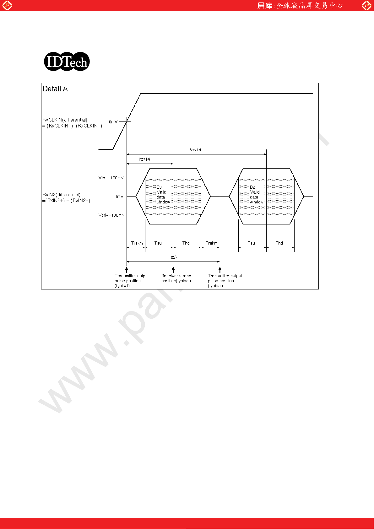
Data Setup Time (Note 2)
Data Hold Time (Note 2)
ps500Tsu
ps500Thd
fc = 82.125MHz,
tCCJ < 50ps,
Vth-Vtl=200mV,
Vcm=1.2V,
Vcm=0
Cycle-to-cycle jitter (Note 3)
Cycle Modulation Rate(Note 4)
fc = 82.125MHzps+150-150tCCJ
fc = 82.125MHzps/clk20tCJavg
fc = 82.125MHznstc/7TskeoclkSkew Time between ReCLKIN
and RoCLKIN
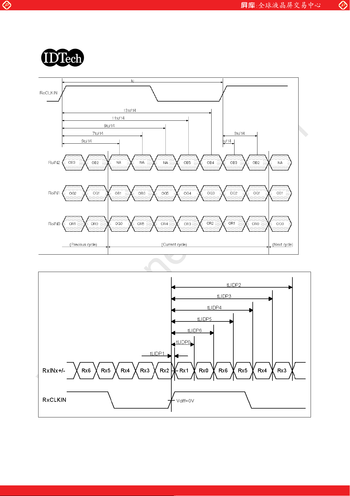
ps5000-500tLIDP1LVDS Input Data Position 1
ps tc/7+500 tc/7 tc/7-500tLIDP0LVDS Input Data Position 2
fc = 82.125MHz
(Note 5)
ps2tc/7+5002tc/72tc/7-500tLIDP6LVDS Input Data Position 3
ps3tc/7+5003tc/73tc/7-500tLIDP5LVDS Input Data Position 4
ps4tc/7+5004tc/74tc/7-500tLIDP4LVDS Input Data Position 5
ps5tc/7+5005tc/75tc/7-500tLIDP3LVDS Input Data Position 6
ps6tc/7+5006tc/76tc/7-500tLIDP2LVDS Input Data Position 7
Note :
1. All values are at VDD=3.3V, Ta=25 degree C.
2. See figure "Timing Definition" and "Timing Definition(detail A)" for definition.
3. Jitter is the magnitude of the change in input clock period.
4. This specification defines maximum average cycle modulation rate in peak-to-peak transition within any
100 clock cycles.
This specification is applied only if input clock peak jitter within any 100 clock cycles is greater than
300ps.
5. See figure "LVDS input Data Position".
(C) Copyright International Display Technology 2001, 2002 All Rights reserved.
June 17,2002 OEM I-910M-03 15/30
One step solution for LCD / PDP / OLED panel application: Datasheet, inventory and accessory!
www.panelook.com
Page 16
Global LCD Panel Exchange Center
Engineering Specification
Figure. Timing Definition (Even Port)
www.panelook.com
(C) Copyright International Display Technology 2001, 2002 All Rights reserved.
June 17,2002 OEM I-910M-03 16/30
One step solution for LCD / PDP / OLED panel application: Datasheet, inventory and accessory!
www.panelook.com
Page 17
Global LCD Panel Exchange Center
Engineering Specification
Figure. Timming Definition (Odd Port)
www.panelook.com
Figure. LVDS Input Data Position
5
(C) Copyright International Display Technology 2001, 2002 All Rights reserved.
June 17,2002 OEM I-910M-03 17/30
One step solution for LCD / PDP / OLED panel application: Datasheet, inventory and accessory!
www.panelook.com
Page 18
Global LCD Panel Exchange Center
Engineering Specification
Figure. Timing Definition (detail A)
www.panelook.com
Note : Tsu and Thd are internal data sampling window of receiver. Trskm is the system skew margin; i.e., the
sum of cable skew, source clock jitter, and other inter-symbol interference, shall be less than Trskm.
(C) Copyright International Display Technology 2001, 2002 All Rights reserved.
June 17,2002 OEM I-910M-03 18/30
One step solution for LCD / PDP / OLED panel application: Datasheet, inventory and accessory!
www.panelook.com
Page 19

Global LCD Panel Exchange Center
Engineering Specification
5.4.2 LVDS Receiver Internal Circuit
Below figure shows the internal block diagram of the LVDS receiver.
www.panelook.com
5.4.3 Recommended Guidelines for Motherboard PCB Design and Cable Selection
Following the suggestions below will help to achieve optimal results.
O Use controlled impedance media for LVDS signals. They should have a matched differential impedance of
100ohm.
O Match electrical lengths between traces to minimize signal skew.
O Isolate TTL signals from LVDS signals.
O For cables, twisted pair, twinax, or flex circuit with close coupled differential traces are recommended.
(C) Copyright International Display Technology 2001, 2002 All Rights reserved.
June 17,2002 OEM I-910M-03 19/30
One step solution for LCD / PDP / OLED panel application: Datasheet, inventory and accessory!
www.panelook.com
Page 20

Global LCD Panel Exchange Center
Engineering Specification
5.5 Signal for Lamp Connector
Signal NamePin #
Lamp High Voltage1
www.panelook.com
2
Lamp Low Voltage
(C) Copyright International Display Technology 2001, 2002 All Rights reserved.
June 17,2002 OEM I-910M-03 20/30
One step solution for LCD / PDP / OLED panel application: Datasheet, inventory and accessory!
www.panelook.com
Page 21

Global LCD Panel Exchange Center
Engineering Specification
6.0 Pixel format image
Following figure shows the relationship of the input signals and LCD pixel format image. Even and odd pair of
RGB data are sampled at a time
Even Odd Even Odd
0 1 2047
www.panelook.com
.
2046
1st Line
1536th Line
R
R
B R
G
B R
G
B
G
B
G
R
R
B R
G
B R
G
B
G
B
G
(C) Copyright International Display Technology 2001, 2002 All Rights reserved.
June 17,2002 OEM I-910M-03 21/30
One step solution for LCD / PDP / OLED panel application: Datasheet, inventory and accessory!
www.panelook.com
Page 22

Global LCD Panel Exchange Center
Engineering Specification
7.0 Parameter guide line for CFL Inverter
www.panelook.com
CONDITIONUNITSMAXTYPMINPARAMETER
White Luminance
(5 points average)
CFL current(ICFL)
-180-
2
(Ta=25 deg.C)cd/m
(Ta=25 deg.C)mArms7.57.03.0
KHz6040CFL Frequency(FCFL)
Vrms--1,500CFL Ignition Voltage(Vs)
Vrms-620-CFL Voltage (Reference)(VCFL)
W9.58.6-CFL Power consumption(PCFL)
(Ta=25 deg.C)
(Note 1)
(Ta= 0 deg.C)
(Note 3)
(Ta=25 deg.C)
(Note 2)
(Ta=25 deg.C)
(Note 2)
Note 1: CFL discharge frequency should be carefully determined to avoid interference between inverter and TFT
LCD.
Note 2:
Calculated value for reference (ICFL x VCFL = PCFL).
Note 3: CFL inverter should be able to give out a power that has a generating capacity of over 1,500 voltage.
Lamp units need 1,500 voltage minimum for ignition.
Note 4:
O All of characteristics listed are measured under the condition using the Test inverter.
O In case of using an inverter other than listed, it is recommended to check the inverter carefully.
Sometimes, interfering noise stripes appear on the screen, and substandard luminance or flicker at low
power may happen.
O In designing an inverter, it is suggested to check safety circuit very carefully.
Impedance of CFL, for instance, becomes more than 1 [M ohm] when CFL is damaged.
O Generally, CFL has some amount of delay time after applying kick-off voltage. It is recommended to
keep on applying kick-off voltage for 1 [Sec] until discharge.
O Reducing CFL current increases CFL discharge voltage and generally increases CFL discharge
frequency. So all the parameters of an inverter should be carefully designed so as not to produce too
much leakage current from high-voltage output of the inverter.
O It should be employed the inverter which has 'Duty Dimming', if ICFL is less than 4.0[mA].
(C) Copyright International Display Technology 2001, 2002 All Rights reserved.
June 17,2002 OEM I-910M-03 22/30
One step solution for LCD / PDP / OLED panel application: Datasheet, inventory and accessory!
www.panelook.com
Page 23

Global LCD Panel Exchange Center
Engineering Specification
The following chart is CFL current versus the luminance for your reference.
www.panelook.com
TBD
(C) Copyright International Display Technology 2001, 2002 All Rights reserved.
June 17,2002 OEM I-910M-03 23/30
One step solution for LCD / PDP / OLED panel application: Datasheet, inventory and accessory!
www.panelook.com
Page 24
Global LCD Panel Exchange Center
Engineering Specification
8.0 Interface Timings
Basically, interface timings described here is not actual input timing of LCD module but output timing of
SN75LVDS86(Texas Instruments) or equivalent.
8.1 Timing Characteristics
www.panelook.com
UnitMAX.TYP.MIN.SymbolItemSignal
50FdckFreqencyDTCLK
[MHz]86.682.125
[ns]20.00012.17711.547Tck
[Hz]-49.266-FvFrame Rate+V-Sync
[ms]-20.3-Tv
[lines]166215551542Nv
[us]-13.1-TvaV-Active Level
[lines]12411Nva
[lines]12411NvbV-Back Porch
[lines]124171NvfV-Front Porch
[lines]1536mV-Line+DSPTMG
[KHz]-76.6-FhScan Rate+H-Sync
[us]-13.1-Th
[Tck]140710721064Nh
[us]0.097ThaH-Active Level
[Tck]38181Nha
[Tck]381321ThbH-Back Porch
[Tck]38181ThfH-Front Porch
[us]12.469ThdDisplay+DSPTMG
[dots]2048nData Even/Odd+DATA
Note :
O Both positive Hsync and positive Vsync polarity is recommended
O When there are invalid timing, Display appears black pattern.
Synchronous Signal Defects and enter Auto Refresh for LCD Module Protection Mode.
(C) Copyright International Display Technology 2001, 2002 All Rights reserved.
June 17,2002 OEM I-910M-03 24/30
One step solution for LCD / PDP / OLED panel application: Datasheet, inventory and accessory!
www.panelook.com
Page 25

Global LCD Panel Exchange Center
Engineering Specification
8.2 Timing Definition
Vertical Timing
www.panelook.com
Support mode
2048 x 1536 at 50Hz
(H line rate : 13.1 us)
DSPTMG
-VSYNC
+VSYNC
Horizontal Timing
Support mode
2048 x 1536
Dotclock : 164.250
MHz (82.125MHz x2)
Tvblk
Vertical
Blanking
0.248 ms
(19 lines)
Tvf
Thblk
Horizontal
Blanking
0.584 us
(96 dots)
Tvblk
Tva
m
Active Field
20.050 ms
(1536 lines)
Tvb
Thd
Active Field
12.469 us
(2048 dots)
Tvf VSYNC
Front Porch
0.222 ms
(17 lines)
Tv
Thf
HSYNC
Front Porch
0.097 us
(16 dots)
Tv,Nv
Frame
Time
20.298 ms
(1555 lines)
m
Th,Nh
H Line
Time
13.053 us
(2144 dots)
Tva
VSYNC
Width
0.013 ms
(1 line)
Tha
HSYNC
Width
0.097 us
(16 dots)
Tvb
VSYNC
Back Porch
0.013 ms
(1 line)
Thb
HSYNC
Back Porch
0.390 us
(64 dots)
DSPTMG
Th
Thf
Thblk Thd
Tha
Thb
-HSYNC
+HSYNC
Tck
VIDEO(Even)
VIDEO(Even)
VIDEO(Odd)
VIDEO(Odd)
0
1
4
2
5
3
n-4 n-2
n-3
n-1
DTCLK
(C) Copyright International Display Technology 2001, 2002 All Rights reserved.
June 17,2002 OEM I-910M-03 25/30
One step solution for LCD / PDP / OLED panel application: Datasheet, inventory and accessory!
www.panelook.com
Page 26

Global LCD Panel Exchange Center
Engineering Specification
9.0 Power Consumption
Input power specifications are as follows;
VDD
Voltage
VDDrp
Drive Ripple Voltage
VDDns
Drive Ripple Noise
Note :Max Pattern:2 dot Vertical sub-pixel stripe.
www.panelook.com
CONDITIONUNITSMaxTypMinPARAMETERSYMBOL
Load Capacitance
V3.63.33.0Logic/LCD Drive
68uF
W5.2VDD PowerPDD
W4.1VDD PowerPDD
mA1730VDD Current IDD
mA1240VDD Current IDD
mVp-p100Allowable Logic/LCD
mVp-p100Allowable Logic/LCD
MAX Pattern
VDD=3.6V
All White Pattern
VDD=3.3V
MAX Pattern
VDD=3.0V
All White Pattern
VDD=3.3V
(C) Copyright International Display Technology 2001, 2002 All Rights reserved.
June 17,2002 OEM I-910M-03 26/30
One step solution for LCD / PDP / OLED panel application: Datasheet, inventory and accessory!
www.panelook.com
Page 27

Global LCD Panel Exchange Center
Engineering Specification
10.0 Power ON/OFF Sequence
VDD power and lamp on/off sequence is as follows. Interface signals are also shown in the chart. Signals from
any system shall be Hi-Z state or low level when VDD is off.
www.panelook.com
150ms min.
VDD
10%
0 V
Signals
0 V
(Recommended).
Lamp
90%
10ms max.
0 min.
90% 90%
10% 10%
100ms min.
180ms min.
90%
20ms min.
On
10% 10%
0 min.
(C) Copyright International Display Technology 2001, 2002 All Rights reserved.
June 17,2002 OEM I-910M-03 27/30
One step solution for LCD / PDP / OLED panel application: Datasheet, inventory and accessory!
www.panelook.com
Page 28
Global LCD Panel Exchange Center
Engineering Specification
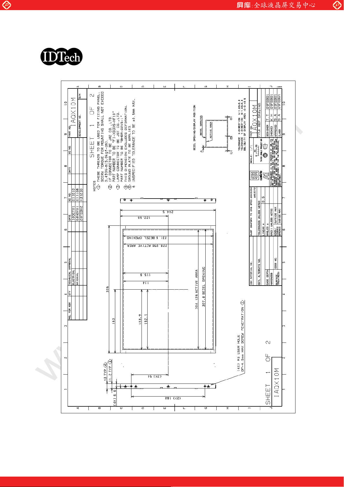
11.0 Mechanical Characteristics
www.panelook.com
(C) Copyright International Display Technology 2001, 2002 All Rights reserved.
June 17,2002 OEM I-910M-03 28/30
One step solution for LCD / PDP / OLED panel application: Datasheet, inventory and accessory!
www.panelook.com
Page 29

Global LCD Panel Exchange Center
Engineering Specification
www.panelook.com
(C) Copyright International Display Technology 2001, 2002 All Rights reserved.
June 17,2002 OEM I-910M-03 29/30
One step solution for LCD / PDP / OLED panel application: Datasheet, inventory and accessory!
www.panelook.com
Page 30

Global LCD Panel Exchange Center
Engineering Specification
12.0 National Test Lab Requirement
The display module is authorized to Apply the UL Recognized Mark.
Conditions of Acceptability
O This component has been judged on the basis of the required spacings in the Standard for Safety of
Information Technology Equipment, Including Electrical Business Equipment, CAN/CSA C22.2
No.950-00,UL60950, 3rd Edition, IEC 60950 (3rd. Ed.) and EN 60950 (3rd. Ed.), which would cover the
component itself if submitted for Listing.
O CF Lamp circuit for this model should be supplied from Limited Current Circuit.
O The units are supplied by Limited Power Sources.
O The terminals and connectors are suitable for factory wiring only.
O The terminals and connectors have not been evaluated for field wiring.
O A suitable Electrical and Fire enclosure shall be provided.
www.panelook.com
****** End Of Page ******
(C) Copyright International Display Technology 2001, 2002 All Rights reserved.
June 17,2002 OEM I-910M-03 30/30
One step solution for LCD / PDP / OLED panel application: Datasheet, inventory and accessory!
www.panelook.com
 Loading...