

Page 1
Automotive VersaClock® 6E Register
Descriptions and Programming Guide
Register Descriptions
The register descriptions section describes the behavior and function of the customer-programmable non-volatile-memory registers in the
VersaClock 6E clock generators.
Table 1. Automotive VersaClock 6E Product(s)
Product Description Package
5P49V60 5-Output VersaClock 6E (automotive, AEC-Q100) 24 pins
For details of product operation, refer to the product datasheet.
VersaClock 6E Register Set
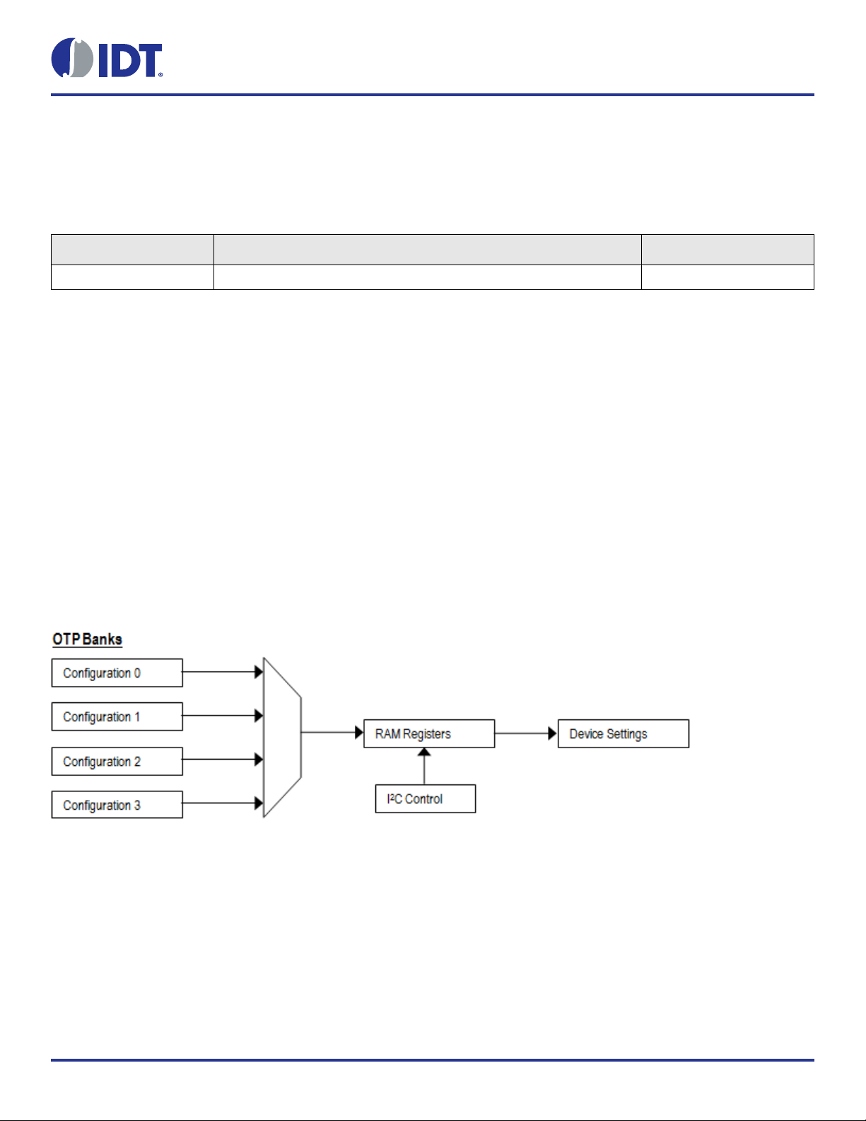
The device contains volatile (RAM) 8-bit registers and non-volatile 8-bit registers (Figure 1). The non-volatile registers are One-Time
Programmable (OTP), and bit values can only be changed from 1 (unburned state) to 0.
The OTP registers include factory trim data and four user configuration tables (Figure 1, Table 3). This document does not describe the
format or methods for programming factory trim data, which is programmed by the factory before shipment.
Each configuration table contains all the information to set up the device's output frequencies. When these configuration tables are
programmed, the device will automatically load the RAM registers with the desired configuration on power-up. The device initializes in
2
either I
mode until power is toggled (Table 2). When powered up in I²C mode, the first configuration table, CFG0, is loaded. When powered up in
selection-pin mode, the SEL0 and SEL1 inputs are decoded to select one of the four configuration tables CFG0-CFG3.
The RAM registers (Table 4) include Status registers for read-back of the device's operating conditions in I
Figure 1. Register Maps
C mode or selection-pin mode, depending on the state of the OUT0/SELB_I2C pin on power-up, and remains in the selected
2
C mode.
1©2019 Integrated Device Technology, Inc. June 7, 2019
Page 2

Automotive VersaClock® 6E Register Descriptions and Programming Guide
Contents
Register Descriptions . . . . . . . . . . . . . . . . . . . . . . . . . . . . . . . . . . . . . . . . . . . . . . . . . . . . . . . . . . . . . . . . . . . . . . . . . . . . . . . . . . . . . . . . . . . . . . 1
VersaClock 6E Register Set. . . . . . . . . . . . . . . . . . . . . . . . . . . . . . . . . . . . . . . . . . . . . . . . . . . . . . . . . . . . . . . . . . . . . . . . . . . . . . . . . . . . . . . . . 1
User Configuration Table Selection . . . . . . . . . . . . . . . . . . . . . . . . . . . . . . . . . . . . . . . . . . . . . . . . . . . . . . . . . . . . . . . . . . . . . . . . . . . . . . . . . . . 3
I2C Interface and Register Access. . . . . . . . . . . . . . . . . . . . . . . . . . . . . . . . . . . . . . . . . . . . . . . . . . . . . . . . . . . . . . . . . . . . . . . . . . . . . . . . . . . . 3
VersaClock 6E Family Power-Up Behavior . . . . . . . . . . . . . . . . . . . . . . . . . . . . . . . . . . . . . . . . . . . . . . . . . . . . . . . . . . . . . . . . . . . . . . . . . . . . . 4
OTP Programming . . . . . . . . . . . . . . . . . . . . . . . . . . . . . . . . . . . . . . . . . . . . . . . . . . . . . . . . . . . . . . . . . . . . . . . . . . . . . . . . . . . . . . . . . . . . . . . . 5
In-System VersaClock 6E OTP Non-Volatile Programming via I2C . . . . . . . . . . . . . . . . . . . . . . . . . . . . . . . . . . . . . . . . . . . . . . . . . . . . . . 6
Default Register Values . . . . . . . . . . . . . . . . . . . . . . . . . . . . . . . . . . . . . . . . . . . . . . . . . . . . . . . . . . . . . . . . . . . . . . . . . . . . . . . . . . . . . . . 6
OTP Control Register . . . . . . . . . . . . . . . . . . . . . . . . . . . . . . . . . . . . . . . . . . . . . . . . . . . . . . . . . . . . . . . . . . . . . . . . . . . . . . . . . . . . . . . . . 7
Factory Reserved Registers for Internal Use Only . . . . . . . . . . . . . . . . . . . . . . . . . . . . . . . . . . . . . . . . . . . . . . . . . . . . . . . . . . . . . . . . . . . 7
Configuration Registers . . . . . . . . . . . . . . . . . . . . . . . . . . . . . . . . . . . . . . . . . . . . . . . . . . . . . . . . . . . . . . . . . . . . . . . . . . . . . . . . . . . . . . . 12
Configuration Register Detail and Functionality Description . . . . . . . . . . . . . . . . . . . . . . . . . . . . . . . . . . . . . . . . . . . . . . . . . . . . . . . . . . . . . . . 15
Shutdown Function . . . . . . . . . . . . . . . . . . . . . . . . . . . . . . . . . . . . . . . . . . . . . . . . . . . . . . . . . . . . . . . . . . . . . . . . . . . . . . . . . . . . . . . . . . 15
Case 1: Output Disable . . . . . . . . . . . . . . . . . . . . . . . . . . . . . . . . . . . . . . . . . . . . . . . . . . . . . . . . . . . . . . . . . . . . . . . . . . . . . . . . . . . 15
Case 2: Shutdown . . . . . . . . . . . . . . . . . . . . . . . . . . . . . . . . . . . . . . . . . . . . . . . . . . . . . . . . . . . . . . . . . . . . . . . . . . . . . . . . . . . . . . 15
Setting Up a Low-Power Shutdown Mode through I2C . . . . . . . . . . . . . . . . . . . . . . . . . . . . . . . . . . . . . . . . . . . . . . . . . . . . . . . . . . 17
Crystal Load Capacitor Registers . . . . . . . . . . . . . . . . . . . . . . . . . . . . . . . . . . . . . . . . . . . . . . . . . . . . . . . . . . . . . . . . . . . . . . . . . . . . . . . 18
Short Example of Programming Crystal . . . . . . . . . . . . . . . . . . . . . . . . . . . . . . . . . . . . . . . . . . . . . . . . . . . . . . . . . . . . . . . . . . . . . . 18
PLL Pre-Divider Options . . . . . . . . . . . . . . . . . . . . . . . . . . . . . . . . . . . . . . . . . . . . . . . . . . . . . . . . . . . . . . . . . . . . . . . . . . . . . . . . . . . . . . 20
PLL Fractional Feedback Divider and Loop Filter . . . . . . . . . . . . . . . . . . . . . . . . . . . . . . . . . . . . . . . . . . . . . . . . . . . . . . . . . . . . . . . . . . . 21
PLL Loop Filter Settings . . . . . . . . . . . . . . . . . . . . . . . . . . . . . . . . . . . . . . . . . . . . . . . . . . . . . . . . . . . . . . . . . . . . . . . . . . . . . . . . . . 25
Fractional Output Dividers and Spread Spectrum . . . . . . . . . . . . . . . . . . . . . . . . . . . . . . . . . . . . . . . . . . . . . . . . . . . . . . . . . . . . . . . . . . . 26
Example of FOD calculation for SSCE = 1 . . . . . . . . . . . . . . . . . . . . . . . . . . . . . . . . . . . . . . . . . . . . . . . . . . . . . . . . . . . . . . . . . . . . 29
Output Divider Control Settings (Table 47 through Table 50) . . . . . . . . . . . . . . . . . . . . . . . . . . . . . . . . . . . . . . . . . . . . . . . . . . . . . . 31
Output Divider Integer Settings (Table 51 through Table 58) . . . . . . . . . . . . . . . . . . . . . . . . . . . . . . . . . . . . . . . . . . . . . . . . . . . . . . 33
Output Divider Fractional and Spread Settings (Table 59 through Table 94) . . . . . . . . . . . . . . . . . . . . . . . . . . . . . . . . . . . . . . . . . . 35
Skew . . . . . . . . . . . . . . . . . . . . . . . . . . . . . . . . . . . . . . . . . . . . . . . . . . . . . . . . . . . . . . . . . . . . . . . . . . . . . . . . . . . . . . . . . . . . . . . . . . . . . 48
Output Divider Skew Integer and Fractional Part Registers Settings (Table 95 through Table 107) . . . . . . . . . . . . . . . . . . . . . . . . . . . . 49
Clock Output Configurations Registers . . . . . . . . . . . . . . . . . . . . . . . . . . . . . . . . . . . . . . . . . . . . . . . . . . . . . . . . . . . . . . . . . . . . . . . . . . . 54
Revision History . . . . . . . . . . . . . . . . . . . . . . . . . . . . . . . . . . . . . . . . . . . . . . . . . . . . . . . . . . . . . . . . . . . . . . . . . . . . . . . . . . . . . . . . . . . . . . . . . 58
2©2019 Integrated Device Technology, Inc. June 7, 2019
Page 3

Automotive VersaClock® 6E Register Descriptions and Programming Guide
User Configuration Table Selection
At power-up, the voltage at OUT0_SEL_I2CB pin 24 is latched by the part and used to select the state of SEL0/SCL pin 9 and SEL1/SDA
pin 8 (Table 2).
If a weak pull-up (10kΩ) is placed on OUT0_SEL_I2CB, the SEL0/SCL and SEL1/SDA pins will be configured as hardware select inputs,
SEL0 and SEL1. Connecting SEL0 and SEL1 to VDDD and/or GND selects one of 4 configuration register sets, CFG0 through CFG3,
which is then loaded into the non-volatile configuration registers to configure the clock synthesizer.
If a weak pull-down is placed on OUT0_SEL_I2CB (or if it is left floating to use internal pull-down), the pins SEL0 and SEL1 will be
configured as a I
configuration registers to configure the clock synthesizer. The host system can use the I
2
C interface's SDA and SCL slave bus. Configuration register set CFG0 is always loaded into the non-volatile
2
C bus to update the non-volatile configuration
registers to change the configuration, and to read status registers.
Table 2. Power-Up Setting of Hardware Select Pin vs I2C Mode, and Default OTP Configuration Register
OUT0_SEL_I2CB Strap at
Power-Up
10kΩ pull-up
10kΩ pull-down or floating SDA SCL
SEL1/SDA pin SEL0/SCL pin Function
0 0 OTP bank CFG0 used to initialize RAM configuration registers.
0 1 OTP bank CFG1 used to initialize RAM configuration registers.
1 0 OTP bank CFG2 used to initialize RAM configuration registers.
1 1 OTP bank CFG3 used to initialize RAM configuration registers.
2
I
C bus enabled to access registers.
OTP bank CFG0 used to initialize RAM configuration registers.
I2C Interface and Register Access
When powered up in I2C mode (Table 2), the device allows access to internal RAM registers (Table 4). The OTP registers (Table 3) are
programmed by loading the desired values into the RAM registers that shadow the target OTP registers (Table 4), and initiating the
internal programming sequence for the desired register range.
Users should not write to the Trim RAM in address range 0x01–0x0F, or the Test RAM in address range 0x6A–0x6F, and should only write
to the OTP Control in address range 0x70–0x7F when programming the OTP.
The RAM in address range 0x80–0x8F is not used by the device and may be used for any purpose.
Table 3. OTP Register Map Summary
Register Range OTP Register Block Name Register Block Description
0x000 OTP Control OTP burned status & I²C address setting.
0x001–0x00F Trim Presets Program default settings. See page 6.
0x010–0x069 CFG0 User configuration settings bank 0.
0x06A–0x0C3 CFG1 User configuration settings bank 1.
0x0C4–0x11D CFG2 User configuration settings bank 2.
0x11E–0x177 CFG3 User configuration settings bank 3.
0x178–0x1AF Factory Use Factory settings–do not over-program.
3©2019 Integrated Device Technology, Inc. June 7, 2019
Page 4
Table 4. RAM Register Map Summary
Automotive VersaClock® 6E Register Descriptions and Programming Guide
Register Range RAM Register Block
0x00 OTP Control OTP Control 0x000
0x01–0x0F Trim Trim 0x000–0x00F
0x10–0x1F Configuration–Main
0x20–0x2F Configuration–CLK1
0x30–0x3F Configuration–CLK2
0x40–0x4F Configuration–CLK3
0x50–0x5F Configuration–CLK4
0x60–0x69 Configuration–Outputs
0x6A–0x6F Factory Use — —
0x70–0x7F OTP Control — —
0x80–0x8F Unused RAM — —
0x90–0x9F Factory Use — —
Corresponding OTP Register
Block Name
CFG0
CFG1
CFG2
CFG3
Corresponding OTP Register Block Address
Range
0x010–0x069
0x06A–0x0C3
0x0C4–0x11D
0x11E–0x177
VersaClock 6E Family Power-Up Behavior
On power-up, the following RAM register loading sequence occurs:
1. The RAM registers always initialize to a hard-wired set of default values, which are also the 'Default register values' for OTP shown in
subsequent tables.
2. If OTP_ burned bit D7 = 0 in the OTP Control register (Table 7), this indicates that the both the Trim OTP tables and at least one of
the four OTP user configuration tables have been programmed.
• Factory programmed product is typically shipped in this condition. Device has factory trim performed and with required
customization written into OTP memory. IDT programs user customization at factory test. Please visit our website for device
customization request.
• Trim RAM data will be updated from the Trim OTP registers into the appropriate trim RAM registers, overwriting the initial default
values.
• Configuration data will be read from the one of the four OTP user configuration tables into the appropriate configuration RAM
registers, overwriting the initial default values. When powered up in I
powered up in selection-pin mode, the SEL0 and SEL1 input pins are decoded to select one of the four configuration tables (Table
23).
• Initialization is now complete, and the part will operate per the configuration settings.
3. If OTP_ burned bit D7 = 1 in the OTP Control register (Table 7), this indicates that the four OTP user configuration tables are
unconfigured.
• Un-programmed product is shipped in this condition and ready for user self-program and customization.
• Configuration RAM data remains at the hard-wired set of default values.
• Initialization is now complete, and the part will operate per the default configuration settings.
• When powered up in I
2
C mode, the Configuration RAM registers can be written with the user's desired settings by the host system,
and the clock generator operated without ever programming any of the four OTP user configuration tables. Alternatively, the host
system (or a programming system) can program one of more of the four OTP user configuration tables, and also clear the OTP_
burned bit D7 in the OTP Control register (Table 7) to 0. The VersaClock 6E device will follow the behavior according to section 0
above for subsequent power ups.
2
C mode, the first configuration table, CFG0, is loaded. When
4©2019 Integrated Device Technology, Inc. June 7, 2019
Page 5
Automotive VersaClock® 6E Register Descriptions and Programming Guide
OTP Programming
The steps for OTP programming are given in Table 5. The procedure is to write the desired default data to the appropriate RAM registers,
and then to instruct the part to burn a desired register address range into OTP.
The RAM registers have an 8-bit register address (0x00 to 0x9F), while the user OTP registers have a 9-bit address (0x000 to 0x177).
This is because there are 4 banks of configuration data in OTP. The OTP addressing therefore extends across two RAM registers (Table
5). The 9-bit user start address is set by register 0x73[7:0] + 0x74[7]. The 9-bit user end address is set by register 0x75[7:0] + 0x76[7].
Table 5. OTP Programming Procedure
Step Procedure Notes
Connect all VDD pins to a single 3.3V, with OUT0_SEL_I2CB pin
0
left floating.
1 Wait 100ms. Part power-up initialization.
Power on the part in I²C mode.
Write device RAM configuration registers 0x10 to 0x69 to the
2
desired state.
3 Write registers 0x73 to 0x78 following the procedure in Table 5.
4 Write register 0x72 = 0xF0. Reset burn bit.
5 Write register 0x72 = 0xF8. Burn the OTP range defined above.
6 Wait 500ms.
7 Write register 0x72 = 0xF0. Reset burn bit.
8 Write register 0x72 = 0xF8. Repeat the burn.
9 Wait 500ms.
10 Write register 0x72 = 0xF0. Reset burn bit.
11 Done programming. Programming complete.
12 Write register 0x72 = 0xF2. Perform margin read.
13 Write register 0x72 = 0xF0. Reset margin read bit.
Read register 0x9F:
14
If bit D1 = 0, programming was successful.
If bit D1 = 1, programming failed.
These RAM values will be programmed into OTP as new
default register values.
Set burn register source address range and destination register
bank CFG0, 1, 2, or 3.
Wait for burn to complete. Device stops acknowledging while
burning.
Wait for burn to complete. Device stops acknowledging while
burning.
Test if OTP programming was successful.
15 Write register 0x9F = 0x00. Reset margin read status bit.
One configuration register bank (CFG0, 1, 2, or 3) is now burned.
16
To burn another bank, repeat the procedure from Step 2.
When all desired configuration register bank have been burned,
17
write device OTP Control register 0x00 with OTP_burned bit D7
clear.
18 Exit. Done.
Burn further configuration register banks if desired.
Burn OTP Control register clearing OTP_burned bit D7. This
sets the part to load configuration data from OTP on power-up.
5©2019 Integrated Device Technology, Inc. June 7, 2019
Page 6
Table 6. OTP Addressing For Programming
Automotive VersaClock® 6E Register Descriptions and Programming Guide
User Start
Register
OTP Control register 0x00 0x4E 0x00 0x61 0x00 0x00 0x00
Configuration CFG0* 0x00 0x4E 0x34 0xE1 0x00 0x00 0x00 to 0x69
Configuration CFG1 0x35 0x4E 0x61 0xE1 0x10 0x10 0x10 to 0x69
Configuration CFG2 0x62 0x4E 0x8E 0xE1 0x10 0x10 0x10 to 0x69
Configuration CFG3 0x8F 0x4E 0xBB 0xE1 0x10 0x10 0x10 to 0x69
Address[8:0]
Part-Select
Bit 0x73
Enable
Sub-block's
Test Mode
0x74
User End
Address[8:0]
Part-Select Bit
0x75
User End
Address[8:0]
Part-Select
Bits 0x76
Burned Register
Start Address
0x77
Read Register
Start Address
0x78
Registers
Burned To
OTP
* Configuration CFG0 includes the Trim presets in 0x01 to 0x0F.
Use the steps in the following example as guidelines to program configuration 0 OTP registers:
1. Write the value from register address 0x00 to 0x69 (first bank) to RAM registers.
Starting at Address 0x00, write data: 61 F3 00 00 00 00 00 00 00 FF FD C0 00 B6 B4 92 A8 CC 81 80 00 03 8C 03 20 00 00 00 9F FF F0
80 00 81 00 00 00 00 00 00 00 00 04 00 01 01 90 00 00 8F 00 00 00 00 00 00 00 00 04 00 00 9C 40 00 00 81 02 00 00 00 00 00 00 00 04
00 00 00 C0 00 00 81 00 00 00 00 00 00 00 00 04 00 00 00 A0 00 3B 01 3B 00 BB 01 7B 01 FF FC
In above example, 61 is the value in register 0x00 that correspond to I
2
C address D4 and the trim presets are recommended defaults:
0x01–0x0F = “F3 00 00 00 00 00 00 00 FF FD C0 00 B6 B4 92".
In above example, a 25MHz crystal is expected, OUT0 is enabled, OUT1 is 50MHz LVCMOS, OUT2 is 10KHz LVCMOS, OUT3 is 100MHz
LVCMOSD and OUT4 is 125MHz LVDS. In case of 5P49V6967 and 5P49V6968, the OUT3 setting will determine the frequency of the
LP-HCSL outputs.
2. Write the following values to program the OTP with config0 and trim bits (Table 6):
• Reg Address (hex): 73 74 75 76 77 78
• Configuration 0: 00 4E 34 E1 00 00
3. Start Burn with Reg 0x72 set to F8.
4. Wait 500ms.
5. Reset Burn Start Bit 0x72 set to F0.
In-System VersaClock 6E OTP Non-Volatile Programming via I2C
For in-system programming of OTP, it is required to power the VDDA and VDDD pins from 3.3V. Other VDD pins can be powered from
1.8V, 2.5V or 3.3V, whatever is needed for the application.
Burning OTP requires a high internal voltage. The circuit responsible for generating the high internal voltage needs at least 3.3V to
generate a high enough internal voltage for reliable OTP burning with good data retention.
Default Register Values
The following tables have a column “Default Value”. These are values as they show in a 5P49V69xxA000, so called “blank” device that is
meant for field programming. When the device is still un-programmed, it runs a default mode with OUT0 enabled and OUT1 = 100MHz,
assuming a 25MHz crystal is connected. The default values are the register settings for this default mode.
6©2019 Integrated Device Technology, Inc. June 7, 2019
Page 7
OTP Control Register
Automotive VersaClock® 6E Register Descriptions and Programming Guide
The I2C slave address can be changed from the default 0xD4 to 0xD0 by programming the I2C_ADDR bit D0. Note that the I2C address
change occurs on the I
D0 should be followed by an I
2
C ACK of the write transaction. An I2C write sequence to register 0x00 that changes the value of I2C_ADDR bit
2
C STOP condition. Further I2C transactions to the part use the new address.
In the OTP Control Register (Table 7) bits can be set for the OTP Burn and OTP Trim status, VC6E or MEMS use and I2C address setting.
Four bits are left unused.
Table 7. RAM0 0x00 – OTP Control Register
Bits Default Value Name Function
It's an active low state that indicates all the OTP burn process is done.
D7 1 OTP_burned
D6 1 OTP_TRIM An active low state that indicates OTP trim part is burned.*
D5 1 Unused Unused.
D4 1 Unused Unused.
D3 1 Unused Unused.
D2 1 Unused Unused.
D1 1 Unused Unused.
D7 = 1 tells the chip that OTP is not burned and it will run the default mode.
D7 = 0 tells the chip that OTP is burned and it will transfer OTP content to the registers for
operating settings.
D0 1 Device I2C_ADDR If I2C_ADDR = 0 then D0 and if I2C_ADDR = 1 then D4.
* The trim values are commonly written with default values and the OTP_TRIM bit is left at “1”.
Factory Reserved Registers for Internal Use Only
Table 8. RAM0 – 0x01: Factory Reserved Bits - Device ID for Chip Identification
Bits Default Value Name Function
D7 1 CFG0_LOCK* Set to “0” to disable burning OTP of Configuration 0.
D6 1 CFG1_LOCK* Set to “0” to disable burning OTP of Configuration 1.
D5 1 CFG2_LOCK* Set to “0” to disable burning OTP of Configuration 2.
D4 1 CFG3_LOCK* Set to “0” to disable burning OTP of Configuration 3.
D3 1 Unused Unused.
D2 1 Unused Unused.
D1 1 Reserved Factory reserved, leave at “1”.
D0 1 Reserved Factory reserved, leave at “1”.
* Configuration Lock bits can be used to prevent future OTP burning that can modify OTP content.
7©2019 Integrated Device Technology, Inc. June 7, 2019
Page 8
Automotive VersaClock® 6E Register Descriptions and Programming Guide
Table 9. RAM0 – 0x02: Factory Reserved Bits - ADC Gain Setting
Bits Default Value Name Function
D7 0
D6 0
D5 0
D4 0
ADC gain[7:0] ADC gain setting - Factory reserved bits
D3 0
D2 0
D1 0
D0 0
Table 10. RAM0 – 0x03: F a cto ry Reserved Bits - ADC Gain Setting
Bits Default Value Name Function
D7 1
D6 1
D5 1
D4 1
ADC gain[15:8] ADC gain setting - Factory reserved bits
D3 1
D2 1
D1 1
D0 1
Table 11. RAM0 – 0x04: F a cto ry Reserved Bits - ADC OFFSET
Bits Default Value Name Function
D7 0
D6 0
D5 0
D4 0
ADC offset[7:0] ADC offset - Factory reserved bits
D3 0
D2 0
D1 0
D0 0
8©2019 Integrated Device Technology, Inc. June 7, 2019
Page 9

Automotive VersaClock® 6E Register Descriptions and Programming Guide
Table 12. RAM0 – 0x05: Factory reserved bits - ADC OFFSET
Bits Default Value Name Function
D7 0
D6 0
D5 0
D4 0
ADC offset[15:8] ADC offset - Factory reserved bits
D3 0
D2 0
D1 0
D0 0
Table 13. RAM0 – 0x06: F actory Reserved Bits
Bits Default Value Name Function
D7 0
D6 0
D5 0
D4 0
TEMPY[7:0] Factory reserved bits
D3 0
D2 0
D1 0
D0 0
Table 14. RAM0 – 0x07: F actory Reserved Bits
Bits Default Value Name Function
D7 0
D6 0
D5 0
D4 0
OFFSET_TBIN<7:0> Unused Factory reserved bits
D3 0
D2 0
D1 0
D0 0
9©2019 Integrated Device Technology, Inc. June 7, 2019
Page 10
Automotive VersaClock® 6E Register Descriptions and Programming Guide
Table 15. RAM0 – 0x08: F actory Reserved Bits
Bits Default Value Name Function
D7 0
D6 0
D5 0
D4 0
GAIN<7:0> Unused Factory reserved bits
D3 0
D2 0
D1 0
D0 0
Table 16. RAM0 – 0x09: F actory Reserved Bits
Bits Default Value Name Function
D7 1
D6 1
test[3:0] Factory reserved bits
D5 1
D4 1
D3 1
D2 1
NP[3:0] Factory reserved bits
D1 1
D0 1
Table 17. RAM0 – 0x0A: Factory Reserved Bits
Bits Default Value Name Function
D7 1 Reserved
D6 1 Reserved
D5 1 Reserved
D4 1 Reserved
Factory reserved bits
D3 1 Reserved
D2 1 Reserved
D1 0 Reserved
D0 1 Reserved
10©2019 Integrated Device Technology, Inc. June 7, 2019
Page 11
Automotive VersaClock® 6E Register Descriptions and Programming Guide
Table 18. RAM0 – 0x0B: Factory Reserved Bits
Bits Default Value Name Function
D7 0
D6 0
D5 0
D4 0
bandgap_trim_up
[5:0]
bandgap voltage trim, one step is 1.2mV higher than current.
D3 0
D2 0
D1 0 unused bit
D0 0 unused bit
Table 19. RAM0 – 0x0C: Factory Reserved Bits
Bits Default Value Name Function
D7 0
D6 0
D5 0
D4 0
bandgap_trim_dn
[5:0]
bandgap voltage trim, one step is 1.2mV lower than current.
D3 0
D2 0
D1 0 unused bit
D0 0 unused bit
Table 20. RAM0 – 0x0D: Factory Reserved Bits
Bits Default Value Name Function
D7 1
clk1_R_trim[2:0] clk_R_trim: trim for “R” variation, 1LSB is 10%, default is in the middle level.D6 0
D5 1
D4 1
clk2_R_trim[2:0] clk_R_trim: trim for “R” variation, 1LSB is 10%, default is in the middle level.D3 0
D2 1
D1 1 CLK4_amp[2] clk_amp: tune the amplitude of PAD, 1LSB is 10%, default is in the middle level.
D0 0 CLK4_amp[1] clk_amp: tune the amplitude of PAD, 1LSB is 10%, default is in the middle level.
11©2019 Integrated Device Technology, Inc. June 7, 2019
Page 12

Automotive VersaClock® 6E Register Descriptions and Programming Guide
Table 21. RAM0 – 0x0E: Factory Reserved Bits
Bits Default Value Name Function
D7 1
clk3_R_trim[2:0] clk_R_trim: trim for “R” variation, 1LSB is 10%, default is in the middle level.D6 0
D5 1
D4 1
clk4_R_trim[2:0] clk_R_trim: trim for “R” variation, 1LSB is 10%, default is in the middle level.D3 0
D2 1
D1 0 CLK4_amp[0] clk_amp: tune the amplitude of PAD, 1LSB is 10%, default is in the middle level.
D0 0 CLK3_amp[0] clk_amp: tune the amplitude of PAD, 1LSB is 10%, default is in the middle level.
Table 22. RAM0 – 0x0F: Factory Reserved Bits
Bits Default Value Name Function
D7 1 CLK1_amp[2]
D6 0 CLK1_amp[1]
D5 0 CLK1_amp[0]
D4 1 CLK2_amp[2]
D3 0 CLK2_amp[1]
clk_amp: tune the amplitude of PAD, 1LSB is 10%, default is in the middle level–Factory
reserved bits.
D2 0 CLK2_amp[0]
D1 1 CLK3_amp[2]
D0 0 CLK3_amp[1]
Configuration Registers
The internal RAM configuration registers occupy 0x10 to 0x69 (Table 4). The 4 OTP configuration banks CFG0, CFG1, CFG2, and CFG3
use the same register structure and setting behavior.
The tables with register details refer to the RAM register address for simplicity. Table 23 shows the 3-digit OTP register addresses 0x010
to 0x177 for the four banks of identical configuration registers, and the corresponding RAM register address.
Table 23. RAM and OTP Configuration Registers CFG0, CFG1, CFG2, CFG3 Summary
Register Address
Function
RAM CFG0 CFG1 CFG2 CFG3
0x10 0x010 0x06A 0x0C4 0x11E
0x11 0x011 0x06B 0x0C5 0x11F
0x12 0x012 0x06C 0x0C6 0x120
0x13 0x013 0x06D 0x0C7 0x121
0x14 0x014 0x06E 0x0C8 0x122
0x15 0x015 0x06F 0x0C9 0x123
Primary Source and Shutdown Register
VCO Band and Factory Reserved Bits
Crystal X1 Load Capacitor Register
Crystal X2 Load Capacitor Register
Factory Reserved Register
Reference Divider Register
12©2019 Integrated Device Technology, Inc. June 7, 2019
Page 13
Automotive VersaClock® 6E Register Descriptions and Programming Guide
Table 23. RAM and OTP Configuration Registers CFG0, CFG1, CFG2, CFG3 Summary (Cont.)
Register Address
Function
RAM CFG0 CFG1 CFG2 CFG3
0x16 0x016 0x070 0x0CA 0x124
0x17 0x017 0x071 0x0CB 0x125
0x18 0x018 0x072 0x0CC 0x126
0x19 0x019 0x073 0x0CD 0x127
0x1A 0x01A 0x074 0x0CE 0x128
0x1B 0x01B 0x075 0x0CF 0x129
0x1C 0x01C 0x076 0x0D0 0x12A
0x1D 0x01D 0x077 0x0D1 0x12B
0x1E 0x01E 0x078 0x0D2 0x12C
0x1F 0x01F 0x079 0x0D3 0x12D
0x20 0x020 0x07A 0x0D4 0x12E
0x21 0x021 0x07B 0x0D5 0x12F
0x22 0x022 0x07C 0x0D6 0x130
0x23 0x023 0x07D 0x0D7 0x131
0x24 0x024 0x07E 0x0D8 0x132
0x25 0x025 0x07F 0x0D9 0x133
0x26 0x026 0x080 0x0DA 0x134
VCO Control Register and Pre-Divider
Feedback Integer Divider Register
Feedback Integer Divider Bits
Feedback Fractional Divider Register
Feedback Fractional Divider Register
Feedback Fractional Divider Register
Factory Reserved Register
Factory Reserved Register
RC Control Register
RC Control Register
Unused Factory Reserved Register
Output Divider 1 Control Register Settings
Output Divider 1 Fractional Settings
Output Divider 1 Fractional Settings
Output Divider 1 Fractional Settings
Output Divider1 Fractional Settings
Output Divider 1 Step Spread Configuration Register
0x27 0x027 0x081 0x0DB 0x135
0x28 0x028 0x082 0x0DC 0x136
0x29 0x029 0x083 0x0DD 0x137
0x2A 0x02A 0x084 0x0DE 0x138
0x2B 0x02B 0x085 0x0DF 0x139
0x2C 0x02C 0x086 0x0E0 0x13A
0x2D 0x02D 0x087 0x0E1 0x13B
0x2E 0x02E 0x088 0x0E2 0x13C
0x2F 0x02F 0x089 0x0E3 0x13D
0x30 0x030 0x08A 0x0E4 0x13E
0x31 0x031 0x08B 0x0E5 0x13F
0x32 0x032 0x08C 0x0E6 0x140
0x33 0x033 0x08D 0x0E7 0x141
0x34 0x034 0x08E 0x0E8 0x142
0x35 0x035 0x08F 0x0E9 0x143
0x36 0x036 0x090 0x0EA 0x144
0x37 0x037 0x091 0x0EB 0x145
Output Divider 1 Step Spread Configuration Register
Output Divider 1 Step Spread Configuration Register
Output Divider 1 Spread Modulation Rate Configuration Register
Output Divider 1 Spread Modulation Rate Configuration Register
Output Divider 1 Skew Integer Part
Output Divider 1 Skew Integer Part
Output Divider 1 Integer Part
Output Divider 1 Integer Part
Output Divider 1 Skew Fractional part
Unused Factory Reserved Register
Output Divider 2 Control Register Settings
Output Divider 2 Fractional Settings
Output Divider 2 Fractional Settings
Output Divider 2 Fractional Settings
Output Divider2 Fractional Settings
Output Divider 2 Step Spread Configuration Register
Output Divider 2 Step Spread Configuration Register
13©2019 Integrated Device Technology, Inc. June 7, 2019
Page 14

Automotive VersaClock® 6E Register Descriptions and Programming Guide
Table 23. RAM and OTP Configuration Registers CFG0, CFG1, CFG2, CFG3 Summary (Cont.)
Register Address
Function
RAM CFG0 CFG1 CFG2 CFG3
0x38 0x038 0x092 0x0EC 0x146
0x39 0x039 0x093 0x0ED 0x147
0x3A 0x03A 0x094 0x0EE 0x148
0x3B 0x03B 0x095 0x0EF 0x149
0x3C 0x03C 0x096 0x0F0 0x14A
0x3D 0x03D 0x097 0x0F1 0x14B
0x3E 0x03E 0x098 0x0F2 0x14C
0x3F 0x03F 0x099 0x0F3 0x14D
0x40 0x040 0x09A 0x0F4 0x14E
0x41 0x041 0x09B 0x0F5 0x14F
0x42 0x042 0x09C 0x0F6 0x150
0x43 0x043 0x09D 0x0F7 0x151
0x44 0x044 0x09E 0x0F8 0x152
0x45 0x045 0x09F 0x0F9 0x153
0x46 0x046 0x0A0 0x0FA 0x154
0x47 0x047 0x0A1 0x0FB 0x155
0x48 0x048 0x0A2 0x0FC 0x156
Output Divider 2 Step Spread Configuration Register
Output Divider 2 Spread Modulation Rate Configuration Register
Output Divider 2 Spread Modulation Rate Configuration Register
Output Divider 2 Skew Integer Part
Output Divider 2 Skew Integer Part
Output Divider 2 Integer Part
Output Divider 2 Integer Part
Output Divider 2 Skew Fractional part
Unused Factory Reserved Register
Output Divider 3 Control Register Settings
Output Divider 3 Fractional Settings
Output Divider 3 Fractional Settings
Output Divider 3 Fractional Settings
Output Divider 3 Fractional Settings
Output Divider 3 Step Spread Configuration Register
Output Divider 3 Step Spread Configuration Register
Output Divider 3 Step Spread Configuration Register
0x49 0x049 0x0A3 0x0FD 0x157
0x4A 0x04A 0x0A4 0x0FE 0x158
0x4B 0x04B 0x0A5 0x0FF 0x159
0x4C 0x04C 0x0A6 0x100 0x15A
0x4D 0x04D 0x0A7 0x101 0x15B
0x4E 0x04E 0x0A8 0x102 0x15C
0x4F 0x04F 0x0A9 0x103 0x15D
0x50 0x050 0x0AA 0x104 0x15E
0x51 0x051 0x0AB 0x105 0x15F
0x52 0x052 0x0AC 0x106 0x160
0x53 0x053 0x0AD 0x107 0x161
0x54 0x054 0x0AE 0x108 0x162
0x55 0x055 0x0AF 0x109 0x163
0x56 0x056 0x0B0 0x10A 0x164
0x57 0x057 0x0B1 0x10B 0x165
0x58 0x058 0x0B2 0x10C 0x166
0x59 0x059 0x0B3 0x10D 0x167
Output Divider 3 Spread Modulation Rate Configuration Register
Output Divider 3 Spread Modulation Rate Configuration Register
Output Divider 3 Skew Integer Part
Output Divider 3 Skew Integer Part
Output Divider 3 Integer Part
Output Divider 3 Integer Part
Output Divider 3 Skew Fractional part
Unused Factory Reserved Register
Output Divider 4 Control Register Settings
Output Divider 4 Fractional Settings
Output Divider 4 Fractional Settings
Output Divider 4 Fractional Settings
Output Divider 4 Fractional Settings
Output Divider 4 Step Spread Configuration Register
Output Divider 4 Step Spread Configuration Register
Output Divider 4 Step Spread Configuration Register
Output Divider 4 Spread Modulation Rate Configuration Register
14©2019 Integrated Device Technology, Inc. June 7, 2019
Page 15
Automotive VersaClock® 6E Register Descriptions and Programming Guide
Table 23. RAM and OTP Configuration Registers CFG0, CFG1, CFG2, CFG3 Summary (Cont.)
Register Address
Function
RAM CFG0 CFG1 CFG2 CFG3
0x5A 0x05A 0x0B4 0x10E 0x168
0x5B 0x05B 0x0B5 0x10F 0x169
0x5C 0x05C 0x0B6 0x110 0x16A
0x5D 0x05D 0x0B7 0x111 0x16B
0x5E 0x05E 0x0B8 0x112 0x16C
0x5F 0x05F 0x0B9 0x113 0x16D
0x60 0x060 0x0BA 0x114 0x16E
0x61 0x061 0x0BB 0x115 0x16F
0x62 0x062 0x0BC 0x116 0x170
0x63 0x063 0x0BD 0x117 0x171
0x64 0x064 0x0BE 0x118 0x172
0x65 0x065 0x0BF 0x119 0x173
0x66 0x066 0x0C0 0x11A 0x174
0x67 0x067 0x0C1 0x11B 0x175
0x68 0x068 0x0C2 0x11C 0x176
0x69 0x069 0x0C3 0x11D 0x177
Output Divider 4 Spread Modulation Rate Configuration Register
Output Divider 4 Skew Integer Part
Output Divider 4 Skew Integer Part
Output Divider 4 Integer Part
Output Divider 4 Integer Part
Output Divider 4 Skew Fractional Part
Clock 1 Output Configuration
Clock 2 Output Configuration
Clock 1 Output Configuration
Clock 2 Output Configuration
Clock 1 Output Configuration
Clock 2 Output Configuration
Clock 1 Output Configuration
Clock 2 Output Configuration
CLK_OE/Shutdown Function
CLK_OS/Shutdown Function
Configuration Register Detail and Functionality Description
Shutdown Function
The shutdown logic offers flexible configuration of shutdown signaling and clock output enable control. The shutdown logic is summarized
in Table 24.
SH bit D0 in the Shutdown register 0x10 (Table 25) configures the SD/OE input's action as either:
▪ Case 1: Output enable (OE) for the clock outputs (leaving the PLL running).
▪ Case 2: Full part shutdown. SH bit D1 = 0 for OE function, or 1 for shutdown function.
Case 1: Output Disable
In output disable mode, individual outputs can be selected to be either Hi-Z or driven high/low, depending on the configuration of the
CLKx_OS and CLKx_OE bits shown in Table 24.
Case 2: Shutdown
When the part is shutdown, the PLL is shutdown, differential outputs are driven High/Low, and the single-ended LVCMOS outputs are
driven low.
With SH (bit D0 in register 0x10) = 0 (“Output Enable” in the part configuration webtool):
▪ When SP bit D1 = 0 in the Shutdown register 0x10 (Table 25), the SD/OE input is active low (“Negative polarity” in the part
configuration webtool). Outputs are active when SD/OE pin is low.
15©2019 Integrated Device Technology, Inc. June 7, 2019
Page 16
Automotive VersaClock® 6E Register Descriptions and Programming Guide
When SP bit D1 = 1, SD/OE is active high (“Positive polarity” in the part configuration webtool). The following sequence shall be applied
to activate the outputs:
1. Startup the VersaClock 6E and wait for PLL to lock.
2. Set the SD/OE pin to 0 (low level).
3. Set the SD/OE pin to 1 (high level).
Table 24. SD/OE Truth Table
Enable
Shutdown
SH bit (D0) SP bit (D1) OSn bit OEn bit
000 x xxTri-state
0 0 1 0 x x Output active
0 0 1 1 x 0 Output active
0 0 1 1 0 1 High-Low
001 1 11Tri-state
010 x xxTri-state
0 1 1 0 x 0 Output active
0 1 1 1 0 0 High-Low
011 1 10Tri-state
011 1 x0
100 x x0Tri-state
1 0 1 0 x 0 Output active
1 0 1 1 x 0 Output active
OE Polarity
Output
Suspend
Output Enable
(only OE)
SD/OE bit SD/OE pin OUTn
→1
Output active (SD/OE pin needs to be first 0, then switched to
1 after PLL lock to activate the outputs)
110 x x0Tri-state
1 1 1 0 x 0 Output active
1 1 1 1 0 0 High-Low
111 1 10Hi-Z
1 x x x 0 1 High-Low
1xx x 11Hi-Z
SH bit = “Shutdown Bit”: Enable shutdown mode where the SD/OE pin can disable more than just outputs.
SP bit = “SD/OE pin Polarity Bit”: Set the polarity of the SD/OE pin where outputs enable or disable. Only works with OE, not with SD.
OSn bit = “Output Suspend Bit”: Permanently disable an output, independent of SD/OE pin.
OEn bit = “Output Enable Bit”: Permanently enable an output, independent of SD/OE pin. Only works with OE, not with SD.
SD/OE bit = “Output Disabled State”: Set the output state to either driven High/Low or Hi-Z when disabled with the SD/OE pin.
SD/OE pin = Physical pin on the device.
SH and SP bits exist only once and affect all outputs. Other bits exist per output and affect that specific output.
16©2019 Integrated Device Technology, Inc. June 7, 2019
Page 17
Automotive VersaClock® 6E Register Descriptions and Programming Guide
Setting Up a Low-Power Shutdown Mode through I2C
1. Tristate the outputs by writing b'001ss000' to registers 0x60, 0x62, 0x64, and 0x66 where ss = 00, 10, or 11 for output clock supply
voltages 1.8V, 2.5V, or 3.3V.
2. Program all outputs to single-ended CMOS by writing 0x00 to registers 0x68.
3. Enable shutdown functionality by either writing 0x83 or 0x43 to register 0x10, for crystal clock source or external clock respectively.
4. Disable all output dividers by writing 0x80 to registers 0x21, 0x31, 0x41, and 0x51.
5. Take the SD/OE input pin 7 high.
Table 25. RAM1 – 0x10: Primary Source and Shutdown Register
Bits Default Value Name Function
D7 1 en_xtal Crystal Oscillator circuit is disabled with 0 and enabled with 1.
D6 0 en_clkin CLKIN differential input circuit is disabled with 0 and enabled with 1.
D5 1 unused Unused Factory reserved bit.
D4 0 unused Unused Factory reserved bit.
Use “en_ref_doubler” is 1 to double the reference frequency for the Phase Frequency
D3 0 en_ref_doubler
Detector.
Use “en_ref_doubler” is 0 to bypass the doubler.
D2 0 en_refmode
D1 0 SP
D0 0
Table 26. RAM6 – 0x68: CLK_OE/Shutdown Function
Bits Default Value Name Function
D7 1 CLK0_OE See Table 24 – This is bit OEn for output 0.
D6 1 CLK1_OE See Table 24 – This is bit OEn for output 1.
D5 1 CLK2_OE See Table 24 – This is bit OEn for output 2.
D4 1 CLK3_OE See Table 24 – This is bit OEn for output 3.
D3 1 CLK4_OE See Table 24 – This is bit OEn for output 4.
D2 1 clk0_slewrate[1]
en_global
shutdown
Enable path from reference clock to OUT1. Set to 1 when OUT1 is a copy of the
reference clock (= OUT0). Set to 0 when using FOD1 for OUT1.
SD/OE input pin is active low if this bit is 0 and active high if this bit is 1. (If D0 = 0 then
D1 reverses SD/OE pin polarity, affecting OE bits in output polarity. If D0 = 1, SD/OE
pin = 1 causes global shutdown).
D1 reverses SD/OE pin polarity, affecting OE bits in output buffers and SD/OE input pin
is shutdown (SD) if this bit is 1.
CLK0 slew rate setting bit[1].
11 = Fastest.
00 = Slowest (20% slower than 11).
D1 1
D0 1
clk0_pwr_sel[1:0]
Clock output driver power supply voltage is indicated by these bits.
D1 D0 = 0x indicates 1.8V.
D1 D0 = 10 indicates 2.5V.
D1 D0 = 11 indicates 3.3V.
17©2019 Integrated Device Technology, Inc. June 7, 2019
Page 18
Automotive VersaClock® 6E Register Descriptions and Programming Guide
R
R
X
Xt al O s cil lator
Cs
C i
Ce
Ce
Table 27. RAM6 – 0x69: CLK_OS/Shutdown Function
Bits Default Value Name Function
D7 1 CLK0_OS CLK_OS checks the shut down truth table. See Shutdown Function section.
D6 1 CLK1_OS CLK_OS checks the shut down truth table. See Shutdown Function section.
D5 1 CLK2_OS CLK_OS checks the shut down truth table. See Shutdown Function section.
D4 1 CLK3_OS CLK_OS checks the shut down truth table. See Shutdown Function section.
D3 1 CLK4_OS CLK_OS checks the shut down truth table. See Shutdown Function section.
D2 1 clk0_slewrate[0] Depends on slew rate (depends on Shutdown function/truth table) – Set slew rate for clk0.
D1 0
otp_pwr_sel[1:0]
D0 0
Set Output Amplitude for OTP voltage:
Factory reserved
Use D1 D0 = 00.
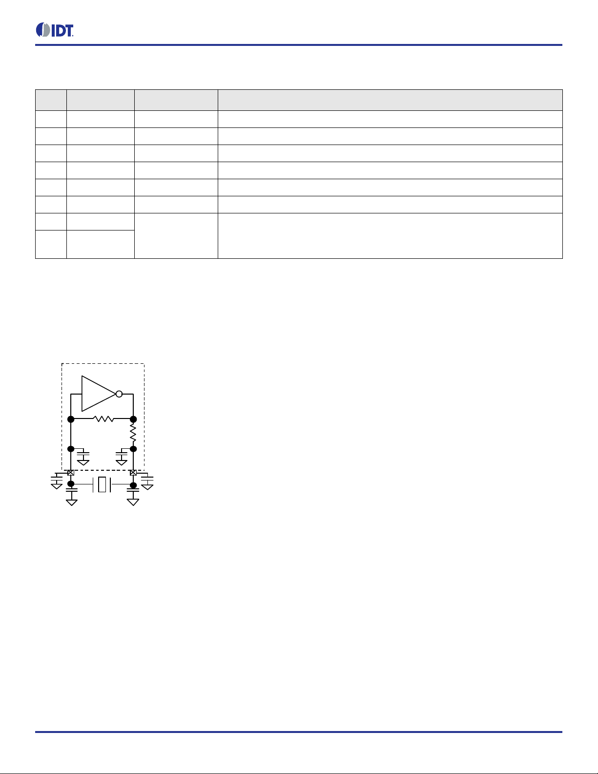
Crystal Load Capacitor Registers
Registers 0x12 and 0x13 are Crystal X1 and X2 Load capacitor registers respectively that are used to add load capacitance to X1 and X2
respectively. In X1 Switch mode is provided with different mode selection options and in X2 polarity selection of clock can be made whose
values are given in the table.
Figure 2. Crystal Oscillator
G
M
F
S
C i
1
2
Cs
X
1
1
1
2
2
2
Short Example of Programming Crystal
Ci1 and Ci2 are on-chip capacitors that are programmable.
Cs is stray capacitance in the PCB and Ce is external capacitors for frequency fine tuning or for achieving load capacitance values
beyond the range of the on-chip programmability.
All these capacitors combined make the load capacitance for the crystal.
• Capacitance on pin X1: Cx1 = Ci1 + Cs1 + Ce1.
• Capacitance on pin X2: Cx2 = Ci2 + Cs2 + Ce2.
• Total Crystal Load Capacitance C
Example: For a Xtal C
C
= (6.92pF+ 7.5pF + 1.5pF)/2 = 7.9pF which is the closest value to 8pF.
L
Here, Cstray = 1.5pF; Package stray = 7.5pF
The binary settings corresponding to this value will be: X1 = X2 = “10000”.
of 8pF, the registers need to be programmed with X1 = X2 = 6.92 pF to get a total
L
= Cx1 × Cx2 / (Cx1 + Cx2).
L
18©2019 Integrated Device Technology, Inc. June 7, 2019
Page 19

Automotive VersaClock® 6E Register Descriptions and Programming Guide
Table 28. RAM1 – 0x12: Crystal X1 Load Capacitor Register
Bits Default Value Name Function
D7 0
Add 6.92pF load capacitance to X1.
D6 0 Add 3.46pF load capacitance to X1.
D5 0 Add 1.73pF load capacitance to X1.
xtal_load_cap_x1[5:0]
D4 0 Add 0.86pF load capacitance to X1.
D3 0 Add 0.43pF load capacitance to X1.
D2 0 Add 0.43pF load capacitance to X1.
D1 0
SM1:0]
D0 1
Table 29. RAM1 – 0x13: F actory Reserved Bits
Bits Default Value Name Function
D7 0
Switch Mode
Factory reserved.
Use D1 D0 = 00.
Add 6.92pF load capacitance to X2.
D6 0 Add 3.46pF load capacitance to X2.
D5 0 Add 1.73pF load capacitance to X2.
xtal_load_cap_x2[5:0]
D4 0 Add 0.86pF load capacitance to X2.
D3 0 Add 0.43pF load capacitance to X2.
D2 0 Add 0.43pF load capacitance to X2.
The PRIMSRC (primary source) bit sets the polarity of the CLKSEL pin.
D1=0: When CLKSEL is Low, Crystal is selected. When CLKSEL is High, CLKIN input is
D1 0 PRIMSRC
selected.
D1=1: When CLKSEL is Low, CLKIN input is selected. When CLKSEL is High, Crystal is
selected.
D0 0 clkok1024 Factory reserved.
Note: The device uses a pre-trimmed integrated crystal. Therefore, bits D7–D2 in registers 0x12 and 0x13 should be set to 1 to prevent
inaccuracy of the output frequencies.
Table 30. RAM1 – 0x14: F actory Reserved Bits
Bits Default Value Name Function
D7 0
D6 0
xtal_reg_amp_sel[3:0] Unused Factory reserved bit.
D5 0
D4 0
19©2019 Integrated Device Technology, Inc. June 7, 2019
Page 20

Automotive VersaClock® 6E Register Descriptions and Programming Guide
Table 30. RAM1 – 0x14: Factory Reserved Bits (Cont.)
Bits Default Value Name Function
D3 0
D2 0
D1 0
D0 0
xtal_I_sel[3:0] Unused Factory reserved bit.
PLL Pre-Divider Options
The reference presented to the fractional PLL can be either directly connected, divided by two or divided by the any value from the range
of three to 127 as set in the register Ref_Div[6:0]. The phase detector of the PLL has a maximum frequency of 150MHz, therefore the
default is to bypass the pre-divider by setting Bypss_prediv = 1 (Table 32). For the functionality of Sel_prediv2 and bypss_prediv bits, see
Figure 3. Table 31 and Table 32 explains the bit selections.
Figure 3. PLL Pre-Divider Options
If pre-divider is selected by selecting bypass_ prediv = 0 (Table 31) then user can select divider by 2 or divider values from 3 to 127.
Table 31. RAM1 – 0x15: Reference Divider Register
Bits Default Value Name Function
D7 0 Sel_prediv2
D6 0
D5 0
D4 0
D3 0
D2 0
D1 0
D0 0
Ref_div[6:0]
Select the divider by 2 function; Divide by 2 if set to 1. And if bypass is set to 0. If divide bit
set 0 and bypass bit set to 0 then reference divider bits (D6 to D0) will take effect.
Reference Divider value.
Use Ref_div setting for values 3 to 127.
Use bit D7 for divide by 2.
Use “Bypass_prediv” bit in Table 32 for divide by 1.
When “Bypass_prediv” is 1, register 0x15 setting is don't care.
When “Sel_prediv2” is 1, Ref_div[6:0] setting is don't care.
20©2019 Integrated Device Technology, Inc. June 7, 2019
Page 21

Automotive VersaClock® 6E Register Descriptions and Programming Guide
Table 32. RAM1 – 0x16: VCO Control Register and Pre-Divider
Bits Default Value Name Function
Use D7 = 1 when phase frequency detector needs to be equal to the reference clock.
D7 1 Bypass_prediv
Use D7 = 0 when the reference clock needs to be divided by at least 2 for the phase
frequency detector. See Table 31 settings.
D6 0 dither_gain_cfg[2]
D5 0 dither_gain_cfg[1]
D4 0 dither_gain_cfg[0]
D3 1 afc_en Open loop vco control is enabled if 1 and disabled if 0–factory reserved bit.
D2 1
cnf_afc[2:0] Open loop vco control voltage bits–factory reserved bits. Use default values.D1 0
D0 0
Table 33. RAM1 – 0x11: VCO Band and Factory Reserved Bits
Bits Default Value Name Function
D7 1 unused Unused Factory reserved bit.
D6 1 unused Unused Factory reserved bit.
D5 0 test_mode_vco_band “test_mode_vco_band” is 1 enables the VCO test mode.
D4 0
D3 1
D2 1
D1 0
vco_band[4:0]
Dither gain settings:
Factory reserved bits.
Use default values.
When bit D5 is 1, it forces the VCO to use the VCO band value in bits D0–4 and ignore
the VCO band (auto) calibration.
D0 0
PLL Fractional Feedback Divider and Loop Filter
Only use the 12-bit integer portion of the PLL Feedback Divider M. The setting FB_intdiv[11:0] is spread out over 2 registers.
The value of M is FVCO / FREF2PLL and care must be taken that M is an integer value.
Example: The circuit uses a 25MHz crystal and we want the VCO to be 2500MHz.
The value of M needs to be 2500 / 25 = 100.
FB_intdiv[11:0] = DEC2HEX(100) = 0 64 or 0000 0110 0100 binary.
21©2019 Integrated Device Technology, Inc. June 7, 2019
Page 22

Automotive VersaClock® 6E Register Descriptions and Programming Guide
Table 34. RAM1 – 0x17: Feedback Integer Divider Register
Bits Default Value Name Function
D7 0
D6 0
D5 0
D4 0
FB_intdiv[11:4] The Feedback Integer Divider Register has 12 bits spread on 2 registers 0x17 and 0x18.
D3 0
D2 1
D1 1
D0 1
Table 35. RAM1 – 0x18: Feedback Integer Divider Bits
Bits Default Value Name Function
D7 0
D6 0
FB_intdiv[3:0] The Feedback Integer Divider Register has 12 bits spread on 2 registers 0x17 and 0x18.
D5 0
D4 0
D3 0 sdm_order_cfg[1] Factory Reserved bits. These both bits are for Sigma Delta Modulator setting.
D3 D2 = 00: sdm bypass,
D3 D2 = 01: selects 1st order,
D2 0 sdm_order_cfg[0]
D3 D2 = 10: selects 2nd order,
D3 D2 = 11: selects 3rd order.
D1 0 i2c_ssce Factory reserved bit.
D0 0 Reserved Factory reserved bit.
Table 36. RAM1 – 0x19: Feedback Fractional Divider Registers
Bits Default Value Name Function
D7 0
D6 0
D5 0
D4 0
FB_frcdiv[23:16]
D3 0
The Feedback fractional divider has 24 bits divided amongst 3 registers (0x19, 0x1A and
0x1B).
D2 0
D1 0
D0 0
22©2019 Integrated Device Technology, Inc. June 7, 2019
Page 23

Automotive VersaClock® 6E Register Descriptions and Programming Guide
Table 37. RAM1 – 0x1A: Feedback Fractional Divider Bits
Bits Default Value Name Function
D7 0
D6 0
D5 0
D4 0
FB_frcdiv[15:8]
D3 0
D2 0
D1 0
D0 0
Table 38. RAM1 – 0x1B: Feedback Fractional Divider Registers
Bits Default Value Name Function
D7 0
D6 0
D5 0
D4 0
FB_frcdiv[7:0
D3 0
D2 0
D1 0
D0 0
The Feedback fractional divider has 24 bits divided amongst 3 registers (0x19, 0x1A
and 0x1B).
The Feedback fractional divider has 24 bits divided amongst 3 registers (0x19, 0x1A and
0x1B).
23©2019 Integrated Device Technology, Inc. June 7, 2019
Page 24

Automotive VersaClock® 6E Register Descriptions and Programming Guide
Table 39. RAM1 – 0x1C: Factory Reserved Bits
Bits Default Value Name Function
D7 1 calibration_start
D6 0
cnf_vreg[1:0]
D5 0
D4 0
cnf_vreg_vco[1:0]
D3 0
D2 1
cnf_vco_bias[1:0]
D1 0
D0 1 en_cp Enable charge pump. Active high.
Needs to be toggled from 0 to 1 to activate the VCO calibration.
Forces VCO band calibration manually.
LDO output voltage adjustment (00, 01, 10, 11).
D6 D5 = 00 or 01 sets LDO to 1.1V,
D6 D5 = 10 sets LDO to 1.2V,
D6 D5 = 11 sets the LDO to 1.25V.
VCO regulator voltage adjustment (00, 01, 10, 11).
D4 D3 = 00 or 01 sets LDO to 1.1V,
D4 D3 = 10 sets LDO to 1.2V,
D4 D3 = 11 sets the LDO to 1.25V.
VCO bias control (00, 01, 10, 11).
D2 D1 = 00 or 01 sets LDO to 1.1V,
D2 D1 = 10 sets LDO to 1.2V,
D2 D1 = 11 sets the LDO to 1.25V.
Note: The Timing Commander software sets more aggressive values in the 0x1C register for slightly improved performance. The Timing
Commander software uses 0x1C = 9F# (1001 1111).
Table 40. RAM1 – 0x1D: Factory Reserved Bits
Bits Default Value Name Function
D7 0
D6 1
D5 1
D4 0
D3 1 en_vco Enable or disable the VCO block.VCO needs to be enabled by default.
D2 1 i2c_bypb_dl
D1 1 temp_sensor_enable
D0 1 en_pll_bias Enable or disable biasing blocks in the PLL. Active high. Enable by default.
cfg_cp[3:0]
1 means the part will reset. Used to re-synchronize the outputs when reprogramming of
Charge-pump current control–Factory reserved bits.
30uA step from 0 to 450uA.
Bypass global reset. 0 means the reset is bypassed.
the device is performed (default value).
Enable temperature sensor.
1 = enable, 0 = disable.
24©2019 Integrated Device Technology, Inc. June 7, 2019
Page 25

Automotive VersaClock® 6E Register Descriptions and Programming Guide
PLL Loop Filter Settings
Figure 4 below shows the Loop Filter components that are programmable via the RC control registers.
Figure 4. PLL Loop Filter Components
where
Rz is programmable with register 0x1E.
Cz is fixed and not programmable. Cz = 500pF.
C2 is the 2nd Pole capacitor and programmable with Register 0x1E.
R3 and C3 are the 3rd pole RC values programmable with register x1F.
The Icp charge pump current is programmable in register x1D.
Table 41. RAM1 – 0x1E: RC Control Register
Bits Default Value Name Function
D7 1
D6 0
D5 1
D4 1
D3 1
D2 0
D1 1
D0 0
lpf_cnf_rz[4:0]
lpf_cnf_cp[2:0]
LPF resistor control, Rz = (31 - cnf_rz) * 1.5K.
1.5K = 11110.
46.5K = 00000.
Setting 11111 is not allowed.
LPF 2nd pole capacitance control.
000 = 12pF to 100 = 28pF step of 4pF.
Settings above 100 are not allowed.
25©2019 Integrated Device Technology, Inc. June 7, 2019
Page 26

Automotive VersaClock® 6E Register Descriptions and Programming Guide
Table 42. RAM1 – 0x1F: RC Control Register
Bits Default Value Name Function
D7 0 p3byp Enable or disable bypass 3rd pole filter
D6 0
D5 1
D4 1
D3 0
D2 0
D1 1
D0 0 cnf_pfddly Phase Frequency Detector delay configuration bit
cnf_p3[5:0]
3rd pole RC configuration. Following values are programmable with bits D1 through D6:
D3D2D1 = 001 → 2kOhm D6D5D4 = 001 → 1.8pF
D3D2D1 = 010 → 8kOhm D6D5D4 = 011 → 3.6pF
D3D2D1 = 011 → 1.6kOhm D6D5D4 = 111 → 5.4pF
D3D2D1 = 100 → 1kOhm.
D3D2D1 = 101 → 7kOhm.
D3D2D1 = 110 → 5.3kOhm.
D3D2D1 = 111 → 1.45kOhm.
Fractional Output Dividers and Spread Spectrum
The output dividers are composed of a 12 bit integer portion, ODx_intdiv[11:0] and a 24 bit fractional portion, ODx_frcdiv[23:0]. “x” is the
output number.
ODx = INT(ODx) + FRAC(ODx) = FVCO / 2 / OUTx (1)
Convert FRAC(ODx) to hex with Eq.2 where ROUND2INT means to round to the nearest integer. The round-off error of ODx in ppm is the
output frequency error in ppm.
ODx_frcdiv[23:0] = DEC2HEX(ROUND2INT[224 * FRAC(ODx)]) (2)
Example: The VCO is 2500MHz and the output needs to be 40MHz.
The output divider value needs to be 2500 / 2 / 40 = 31.25.
Then INT(ODx) = 31 and FRAC(ODx) = 0.25 that gives:
24
2
× FRAC(ODx) = 224 × 0.25 = 4194304
ROUND2INT(4194304) = 4194304
ODx_frcdiv[23:0] = DEC2HEX(4194304) = 40 00 00
Spread spectrum capability is contained within the Fractional-N output dividers associated with each output clock. When applied, triangle
wave modulation of any spread spectrum amount, SS%AMT, from ±0.25% to ±2.5% center spread and - 0.5% to -5% down spread
between 30 and 63kHz may be generated, independent of the output clock frequency. Five variables define spread spectrum in FODx
(see Table 43).
26©2019 Integrated Device Technology, Inc. June 7, 2019
Page 27

Table 43. Spread Spectrum Variables in FODx
Automotive VersaClock® 6E Register Descriptions and Programming Guide
RAM Register
Name Function
ODx_ssce Spread spectrum control enable. 0x25,0x35,0x45,0x55 1
ODx_intdiv
ODx_period
ODx_step Modulation step size.
ODx_offset
Integer portion of the FODx
divider, N.
Spread spectrum modulation
period.
Spread spectrum modulation
offset, which defines down
spread or center spread and is
the fractional portion of the
divider.
(see Table 23)
0x2D, 0x2E,0x3D,0x3E,
0x4D, 0x4E,0x5D,0x5E
0x29,0x2A,0x39,0x3A,
0x49,0x4A,0x59,0x5A
0x26,0x27,0x28,0x36,
0x37,0x38,0x46,0x47,
0x48,0x56,0x57,0x58
0x22,0x23,0x24,0x25,
0x32,0x33,0x34,0x35,
0x42,0x43,0x44,0x45,
0x52,0x53,0x54,0x55
Register
Length
12
13
24
30
Note
If ODx_ssce = 0, contents of ODx_period and
ODx_step are Don't Care.
Defined as half the reciprocal of the modulation
frequency and measured in cycles of the FODx
output frequency.
See equation below.
Sets the time rate of change or time slope of the
output clock frequency.
ODx_offset is the actual spread spectrum offset
subtracted from the Fractional portion of the
FODx divider N. It is the fractional portion of the
FODx divider and accounts for the fact that there
is no ODx_frcdiv in the Memory map.
To calculate the spread spectrum registers (fractional portion), first determine the value in decimal of the FOD output divider, N, for the
nominal output frequency without spread spectrum. The VCO frequency is divided by two to account for a fixed divide by 2 between the
VCO output and the input to the FOD. Convert the integer portion into hex to define ODx_intdiv.
If no spread is to be applied to FODx (ODx_ssce = 0) then ODx_period and ODx_step registers are don't Care and it is permissible to skip
to Eq.9. Convert FRAC(N) to 30 bits as per Eq.10.
When the ODx_period and ODx_step registers are calculated below, ODx_period and ODx_step are explicitly set to 0 if ODx_ssce will
always be 0. This is done for reasons of style, it reinforces the fact that there is no spread spectrum invoked when ODx_ssce = 0. If down
spread is to be turned on by just setting ODx_ssce = 1, then ODx _period and ODx_step must be calculated and registered. See Eq.9 to
see why changing only ODx_ssce works only for down spread.
Consider one cycle of down spread triangular modulation; the output divider, N, is ramped up linearly from the non-spread value of N
followed by a linear ramp back down to the non-spread value of N. N is always greater than or equal to the non-spread value of N,
therefore the output frequency is always less than or equal to the non-spread frequency.
27©2019 Integrated Device Technology, Inc. June 7, 2019
Page 28

Automotive VersaClock® 6E Register Descriptions and Programming Guide
Figure 5. Spread Step and Period
As normally defined, ODx_period (dec) would be 1/ F SS, but the modulation period is defined instead as ½*1/ FSS for the most direct
calculation of ODx_step as will be seen below in the following Equations. An added benefit is that the up ramp and the down ramp are
guaranteed to be symmetric. Note that ODx_period does not have units of time; it is the dimensionless number of FOUT periods that fit in
a half period of FSS.
Calculate the step size.
Since the spread spectrum ramp as implemented only decreases the frequency of FOUT, then the actual offset for down spread is zero.
But if the spread is to be centered, an offset equal to half the peak modulation, SS%AMT *N, is to be subtracted from the value of
FRAC(N).
If FRAC(N) is a small positive value, it is possible that after the center spread offset is subtracted ODx_offset will be negative. In this
case, retain only the lower 30 bits of the 32 bit hex value and assign them to ODx_offfset[29:0].
In this manner it can be seen that ODx_offset is the value of FRAC(N), appropriately adjusted should center spread be enabled.
28©2019 Integrated Device Technology, Inc. June 7, 2019
Page 29

Automotive VersaClock® 6E Register Descriptions and Programming Guide
Example of FOD calculation for SSCE = 1
Out1 of clock1 = 99MHz, spread enabled with total spread 0.5% and SS 31.5KHz.
Doubler enabled, Feedback divider = 53, and VCO = 2650MHz. Let's calculate the FOD 1 value according to the equations above.
FVCO/2 = 2650/2 = 1325, and FOUT = 99MHz (given).
(FVCO/2)/ FOUT = 1325/99 = 13.38383838.
OD1 Integer = 13 then ODx_intdiv[11:0] = 00D hex.
As ssce = 1, ODx_period(dec) = (½) × (FOUT / FSS).
Fss = 31.5kHz and Fout = 99MHz then ODx_period(dec) = 1571.42857143.
Now, from Eq.6, ODx_period [12:0] = 6 23 hex.
From Eq.7, ODx_Step(dec) = [((0.5/100) × (13.38383838)] / 1571 = 0.000042596557.
From Eq.8
→ (0.000042596557 × 2
24
) = 714.651647 then Odx_Step [23:0] = 00 02 CB hex.
From Eq.9, ODx_offset(dec) = 0.38383838 - ((0.5 / 100) × 13.38383838)/ 2] = 0.350378787.
From Eq.10, (2
24
× 0.350378787) = 5878380.605 → Odx_offset [29:0] = 00 59 B2 6D hex.
Some calculated examples with SSCE = 0 for frequency margining purposes:
Table 44. PLL Config ured Values
input clock (MHz) 25
ref_div (real) 0
ref_div (Hex) 0
bypass_pre_div 1
Doubler Enabled
Ref for PLL (MHz) 50
VCO (GHz) 2.6
FB_div (real) 52
FB_intdiv (Hex) 34 Hex
FB_frcdiv (Hex) 00 Hex
Table 45. Output Values with SSCE = 0
Frequency
Margining
-3% 97.000 0 13.402062 00D 66 ED 87 0 0 0 0 0
-2% 98.000 0 13.265306 00D 43 EB 1A 0 0 0 0 0
Output
(MHz)
ssce
Divider
(real)
ODx_intdiv
(HEX)
ODx_offset
(HEX)
Period
(HEX)
Step
(HEX)
Offset
(HEX)
skew_int
(HEX)
skew_frac
(HEX)
-1% 99.000 0 13.131313 00D 21 9D BD 0 0 0 0 0
0% 100.000 0 13.000000 00D 00 00 00 0 0 0 0 0
1% 101.000 0 12.871287 00C DF 0C AC 0 0 0 0 0
2% 102.000 0 12.745098 00C BE BE BE 0 0 0 0 0
3% 103.000 0 12.621359 00C 9F 11 66 0 0 0 0 0
29©2019 Integrated Device Technology, Inc. June 7, 2019
Page 30

Automotive VersaClock® 6E Register Descriptions and Programming Guide
XIN/REF
XOUT
CLKIN
CLKINB
CLKSEL
SD/OE
SEL1/SDA
SEL0/SCL
V
DDA
V
DDD
V
DDO
0
OUT0 _SE L_I2C B
V
DDO
1
OUT1
OUT1B
V
DDO
2
OUT2
OUT2B
V
DDO
3
OUT3
OUT3B
V
DDO
4
OUT4
OUT4B
FOD1
FOD2
FOD3
FOD4
PLL
OTP
and
Control
Logic
en_clkbuf1
0
1
0
1
0
1
0
1
en_clkbuf2
en_clkbuf3
en_clkbuf4
en_fod4
en_fod3
en_fod2
en_fod1
en_refmode
en_aux1
en_aux2
en_aux3
sel_ext1, selb_norm1,
int_mode1
sel_ext2,
selb_norm2,
int_mode2
sel_ext3,
selb_norm3,
int_mode3
sel_ext4,
selb_norm4,
int_mode4
Table 46. FOD1 Register Table
Register Offsets
Output (MHz) 0x22 0x23 0x24 0x25 0x26 0x27 0x28 0x29 0x2A 0x2B 0x2C 0x2C 0x2E 0x2F
97.000 01 9B B6 1C 00 00 00 00 04 00 00 00 D0 00
98.000 01 0F AC 68 00 00 00 00 04 00 00 00 D0 00
99.000 00 86 76 F4 00 00 00 00 04 00 00 00 D0 00
100.000 00 00 00 00 00 00 00 00 04 00 00 00 D0 00
101.000 03 7C 32 B0 00 00 00 00 04 00 00 00 C0 00
102.000 02 FA FA FC 00 00 00 00 04 00 00 00 C0 00
103.000 02 7C 45 98 00 00 00 00 04 00 00 00 C0 00
Figure 6. Output Divider Control Settings Block Diagram
There are a number of MUX circuits to route clocks around and/or through certain fractional output dividers. For example, the output from
FOD1 can be channeled to outputs 1 through 4 so only FOD1 needs to be enabled when all output frequencies are the same. There are
also channeling options to use the output of one FOD to be the input of the following FOD so the output of that second FOD can be a very
low frequency, for example a few kHz. Only when an FOD gets its input clock from the PLL can the fractional part of the divider be used.
When using the clock from a previous output, the FOD can only be used in integer mode. The following pages explain how to set up the
MUX.
30©2019 Integrated Device Technology, Inc. June 7, 2019
Page 31

Automotive VersaClock® 6E Register Descriptions and Programming Guide
Output Divider Control Settings (Table 47 through Table 50)
These bits are for Output divider's control register settings and are reserved in general. The reset bit for the FOD is active low. The
combination of en_fod (fractional output divider enable bit), sel_ext (the output from previous channel FOD) and selb_norm (the output
from current FOD), will set the divider mode. The integer mode only can be enabled with int_mode bit.
Table 47. RAM2 – 0x21: Output Divider 1 Control Register Settings
Default
Bits
D7 1 i2c_resetb1 Reset Fractional Output Divider 1 (FOD1) circuit when set to 0.
D6 0
D4 0
D3 0 selb_norm1 0000: FOD1 and OUT1 are not used.
D2 0 sel_ext1
D1 0 int_mode1
D0 1 en_fod1
Value
Name Function
en_pi_out_cap<2:0> Factory reserved /unused bits.D5 0
00x1: FOD1 uses clock from PLL and OUT1 uses clock from FOD1.
1100: FOD1 disabled and OUT1 uses clock from OUT0. En_refmode needs to be 1.
1111: FOD1 uses clock from OUT0 and OUT1 uses clock from FOD1. En_refmode needs to be 1.
“int_mode1” sets integer mode for FOD1 (fractional settings will be ignored).
Table 48. RAM3 – 0x31: Output Divider 2 Control Register Settings
Bits Default Value Name Function
D7 0 i2c_resetb2 Reset Fractional Output Divider 2 (FOD2) circuit when set to 0.
D6 0
en_pi_out_cap<2:0> Factory reserved /unused bitsD5 0
D4 0
D3 0 selb_norm2 0000: FOD2 and OUT2 are not used.
D2 0 sel_ext2
D1 0 int_mode2
D0 0 en_fod2
00x1: FOD2 uses clock from PLL and OUT2 uses clock from FOD2.
1100: FOD2 disabled and OUT2 uses clock from OUT1. En_aux1 needs to be 1.
1111: FOD2 uses clock from OUT1 and OUT2 uses clock from FOD2. En_aux1 needs to be 1.
“int_mode2” sets integer mode for FOD2 (fractional settings will be ignored).
31©2019 Integrated Device Technology, Inc. June 7, 2019
Page 32

Automotive VersaClock® 6E Register Descriptions and Programming Guide
Table 49. RAM4 – 0x41: Output Divider 3 Control Register Settings
Bits Default Value Name Function
D7 0 i2c_resetb3 Reset Fractional Output Divider 3 (FOD3) circuit when set to 0.
D6 0
en_pi_out_cap<2:0> Factory reserved /unused bits.D5 0
D4 0
D3 0 selb_norm3 0000: FOD3 and OUT3 are not used.
D2 0 sel_ext3
D1 0 int_mode3
D0 1 en_fod3
Table 50. RAM5 – 0x51: Output Divider 4 Control Register Settings
Bits Default Value Name Function
00x1: FOD3 uses clock from PLL and OUT3 uses clock from FOD3.
1100: FOD3 disabled and OUT3 uses clock from OUT2. En_aux2 needs to be 1.
1111: FOD3 uses clock from OUT2 and OUT3 uses clock from FOD3. En_aux2 needs to be 1.
“int_mode3” sets integer mode for FOD3 (fractional settings will be ignored).
D7 0 i2c_resetb4 Reset Fractional Output Divider 4 (FOD4) circuit when set to 0.
D6 0
en_pi_out_cap<2:0> Factory reserved /unused bits.D5 0
D4 0
D3 0 selb_norm4 0000: FOD4 and OUT4 are not used.
D2 0 sel_ext4
D1 0 int_mode4
D0 0 en_fod4
00x1: FOD4 uses clock from PLL and OUT4 uses clock from FOD4.
1100: FOD4 disabled and OUT4 uses clock from OUT3. En_aux3 needs to be 1.
1111: FOD4 uses clock from OUT3 and OUT4 uses clock from FOD4. En_aux3 needs to be 1.
“int_mode4” sets integer mode for FOD1 (fractional settings will be ignored).
32©2019 Integrated Device Technology, Inc. June 7, 2019
Page 33

Automotive VersaClock® 6E Register Descriptions and Programming Guide
Output Divider Integer Settings (Table 51 through Table 58)
Output divider's integer part consists of 12 bits spread on 2 consecutive registers. The 4 dividers are assigned to respectively to each
output: 1, 2, 3, 4.
Table 51. RAM2 – 0x2D: Output Divider 1 Integer Part
Bits Default Value Name Function
D7 0
D6 0
D5 0
D4 0
D3 0
D2 0
D1 0
D0 0
Table 52. RAM2 – 0x2E: Output Divider 1 Integer Part
Bits Default Value Name Function
D7 1
D6 1
D5 1
D4 0
D3 0 unused bits Unused Factory reserved bit.
D2 0 unused bits Unused Factory reserved bit.
D1 0 unused bits Unused Factory reserved bit.
D0 0 unused bits Unused Factory reserved bit.
OD1_intdiv[11:4] Output divider 1 integer part has 12 bit spread over 2 registers x2D and x2E.
OD1_intdiv[3:0] Output divider 1 integer part has 12 bit spread over 2 registers x2D and x2E.
Table 53. RAM3 – 0x3D: Output Divider 2 Integer Part
Bits Default Value Name Function
D7 0
D6 0
D5 0
D4 0
D3 0
D2 0
D1 0
D0 0
OD2_intdiv[11:4] Output divider 2 integer part has 12 bit spread over 2 registers x3D and x3E.
33©2019 Integrated Device Technology, Inc. June 7, 2019
Page 34

Automotive VersaClock® 6E Register Descriptions and Programming Guide
Table 54. RAM3 – 0x3E: Output Divider 2 Integer Part
Bits Default Value Name Function
D7 0
D6 0
OD2_intdiv[3:0] Output divider 2 integer part has 12 bit spread over 2 registers x3D and x3E.
D5 0
D4 0
D3 0 unused bits Unused Factory reserved bit.
D2 0 unused bits Unused Factory reserved bit.
D1 0 unused bits Unused Factory reserved bit.
D0 0 unused bits Unused Factory reserved bit.
Table 55. RAM4 – 0x4D: Output Divider 3 Integer Part
Bits Default Value Name Function
D7 0
D6 0
D5 0
D4 0
OD3_intdiv[11:4] Output divider 3 integer part has 12 bit spread over 2 registers x4D and x4E.
D3 0
D2 0
D1 0
D0 0
Table 56. RAM4 – 0x4E: Output Divider 3 Integer Part
Bits Default Value Name Function
D7 0
D6 0
OD3_intdiv[3:0] Output divider 3 integer part has 12 bit spread over 2 registers x4D and x4E.
D5 0
D4 0
D3 0 unused bits Unused Factory reserved bit.
D2 0 unused bits Unused Factory reserved bit.
D1 0 unused bits Unused Factory reserved bit.
D0 0 unused bits Unused Factory reserved bit.
34©2019 Integrated Device Technology, Inc. June 7, 2019
Page 35

Automotive VersaClock® 6E Register Descriptions and Programming Guide
Table 57. RAM5 – 0x5D: Output Divider 4 Integer Part
Bits Default Value Name Function
D7 0
D6 0
D5 0
D4 0
D3 0
D2 0
D1 0
D0 0
Table 58. RAM5 – 0x5E: Output Divider 4 Integer Part
Bits Default Value Name Function
D7 0
D6 0
D5 0
D4 0
D3 0 unused bits Unused Factory reserved bit.
D2 0 unused bits Unused Factory reserved bit.
D1 0 unused bits Unused Factory reserved bit.
D0 0 unused bits Unused Factory reserved bit.
OD4_intdiv[11:4] Output divider 4 integer part has 12 bit spread over 2 registers x5D and x5E.
OD4_intdiv[3:0] Output divider 4 integer part has 12 bit spread over 2 registers X5D and x5E.
Output Divider Fractional and Spread Settings (Table 59 through Table 94)
ODx_offset is the actual spread spectrum offset subtracted from the Fractional portion of the FODx divider N. It is the fractional portion of
the FODx divider. 30 bits spread over 4 registers. MSB is a sign bit. Set to 1 for negative numbers.
ODx_period bits are used to tune the spread rate from 30KHz to 63KHz according to the output frequency (period = Fout/Fss/2).13 bits
spread on 2 registers.
ODx_step is the Modulation step size; it sets the time rate of change or time slope of the output clock frequency. 24 bits spread on 3
registers.
If ODx_ssce = 0, contents of ODx_period and ODx_step are don't care only the ODx_offset are taken into account.
If ODx_ssce =1, means the spread is enabled for center spread offset. (See example of spread calculation “Example of FOD calculation
for SSCE = 1”)
35©2019 Integrated Device Technology, Inc. June 7, 2019
Page 36

Automotive VersaClock® 6E Register Descriptions and Programming Guide
Table 59. RAM2 – 0x22: Output Divider 1 Fractional Settings
Bits Default Value Name Function
D7 0
D6 0
D5 0
D4 0
OD1_offset[29:22] 30 bits to configure the fraction value of FOD1 in register address. x22, x23, x24 and x25.
D3 0
D2 0
D1 0
D0 0
Table 60. RAM2 – 0x23: Output Divider 1 Fractional Settings
Bits Default Value Name Function
D7 0
D6 0
D5 0
D4 0
OD1_offset[21:14] 30 bits to configure the fraction value of FOD1 in register address x22, x23, x24 and x25.
D3 0
D2 0
D1 0
D0 0
Table 61. RAM2 – 0x24: Output Divider 1 Fractional Settings
Bits Default Value Name Function
D7 0
D6 0
D5 0
D4 0
OD1_offset[13:6] 30 bits to configure the fraction value of FOD1 in register address x22, x23, x24 and x25.
D3 0
D2 0
D1 0
D0 0
36©2019 Integrated Device Technology, Inc. June 7, 2019
Page 37

Automotive VersaClock® 6E Register Descriptions and Programming Guide
Table 62. RAM2 – 0x25: Output Divider 1 Fractional Settings
Bits Default Value Name Function
D7 0
D6 0
D5 0
OD1_offset[5:0] 30 bits to configure the fraction value of FOD1 in register address x22, x23, x24 and x25.
D4 0
D3 0
D2 0
D1 0 OD1_ssce Enable spread spectrum with center spread offset. Active High.
D0 0 Unused Unused Factory reserved bit.
Table 63. RAM2 – 0x26: Output Divider 1 Step Spread Configuration Register
Bits Default Value Name Function
D7 0
D6 0
D5 0
D4 0
OD1_step[7:0] 24 bits used for modulation step size in register x26 x27 and x28.
D3 0
D2 0
D1 0
D0 0
Table 64. RAM2 – 0x27: Output Divider 1 Step Spread Configuration Register
Bits Default Value Name Function
D7 0
D6 0
D5 0
D4 0
OD1_step[15:8] 24 bits used for modulation step size in register x26 x27 and x28.
D3 0
D2 0
D1 0
D0 0
37©2019 Integrated Device Technology, Inc. June 7, 2019
Page 38

Automotive VersaClock® 6E Register Descriptions and Programming Guide
Table 65. RAM2 – 0x28: Output Divider 1 Step Spread Configuration Register
Bits Default Value Name Function
D7 0
D6 0
D5 0
D4 0
OD1_step[23:16] 24 bits used for modulation step size in register x26 x27 and x28.
D3 0
D2 0
D1 0
D0 0
Table 66. RAM2 – 0x29: Output Divider 1 Spread Modulation Rate Configuration Register
Bits Default Value Name Function
D7 0
D6 0
D5 0
D4 0
OD1_period[12:5] 13 bits used to configure spread modulation period in register x29 and x2A.
D3 0
D2 0
D1 0
D0 0
Table 67. RAM2 – 0x2A: Output Divider 1 Spread Modulation Rate Configuration R egister
Bits Default Value Name Function
D7 0
D6 0
D5 0
OD1_period[4:0] 13 bits used to configure spread modulation period in register x29 and x2A.
D4 0
D3 0
D2 0 Unused Bits Unused Factory reserved bit.
D1 0 Unused Bits Unused Factory reserved bit.
D0 0 Unused Bits Unused Factory reserved bit.
38©2019 Integrated Device Technology, Inc. June 7, 2019
Page 39

Automotive VersaClock® 6E Register Descriptions and Programming Guide
Table 68. RAM3 – 0x32: Output Divider 2 Fractional Settings
Bits Default Value Name Function
D7 0
D6 0
D5 0
D4 0
OD2_offset[29:6] 30 bits to configure the fraction value of FOD2 in register address x32, x33, x34 and x35.
D3 0
D2 0
D1 0
D0 0
Table 69. RAM3 – 0x33: Output Divider 2 Fractional Settings
Bits Default Value Name Function
D7 0
D6 0
D5 0
D4 0
OD2_offset[29:6] 30 bits to configure the fraction value of FOD2 in register address x32, x33, x34 and x35.
D3 0
D2 0
D1 0
D0 0
Table 70. RAM3 – 0x34: Output Divider 2 Fractional Settings
Bits Default Value Name Function
D7 0
D6 0
D5 0
D4 0
OD2_offset[29:6] 30 bits to configure the fraction value of FOD2 in register address x32, x33, x34 and x35.
D3 0
D2 0
D1 0
D0 0
39©2019 Integrated Device Technology, Inc. June 7, 2019
Page 40

Automotive VersaClock® 6E Register Descriptions and Programming Guide
Table 71. RAM3 – 0x35: Output Divider 2 Fractional Settings
Bits Default Value Name Function
D7 0
D6 0
D5 0
OD2_offset[5:0] 30 bits to configure the fraction value of FOD2 in register address x32, x33, x34 and x35.
D4 0
D3 0
D2 0
D1 0 OD2_ssce Enable spread spectrum with center spread offset. Active High.
D0 0 unused Bit Unused Factory reserved bit.
Table 72. RAM3 – 0x36: Output Divider 2 Step Spread Configuration Register
Bits Default Value Name Function
D7 0
D6 0
D5 0
D4 0
OD2_step[7:0] 24 bits used for modulation step size in register x36 x37 and x38.
D3 0
D2 0
D1 0
D0 0
Table 73. RAM3 – 0x37: Output Divider 2 Step Spread Configuration Register
Bits Default Value Name Function
D7 0
D6 0
D5 0
D4 0
OD2_step[15:8] 24 bits used for modulation step size in register x36 x37 and x38.
D3 0
D2 0
D1 0
D0 0
40©2019 Integrated Device Technology, Inc. June 7, 2019
Page 41

Automotive VersaClock® 6E Register Descriptions and Programming Guide
Table 74. RAM3 – 0x38: Output Divider 2 Step Spread Configuration Register
Bits Default Value Name Function
D7 0
D6 0
D5 0
D4 0
OD2_step[23:16] 24 bits used for modulation step size in register x36 x37 and x38.
D3 0
D2 0
D1 0
D0 0
Table 75. RAM3 – 0x39: Output Divider 2 Spread Modulation Rate Configuring Register
Bits Default Value Name Function
D7 0
D6 0
D5 0
D4 0
OD2_period[12:5] 13 bits used to configure spread modulation period in register x39 and x3A.
D3 0
D2 0
D1 0
D0 0
Table 76. RAM3 – 0x3A: Output Divider 2 Spread Modulation Rate Configuring Register
Bits Default Value Name Function
D7 0
D6 0
D5 0
OD2_period[4:0] 13 bits used to configure spread modulation period in register x39 and x3A.
D4 0
D3 0
D2 0 unused bit Unused Factory reserved bit.
D1 0 unused bit Unused Factory reserved bit.
D0 0 unused bit Unused Factory reserved bit.
41©2019 Integrated Device Technology, Inc. June 7, 2019
Page 42

Automotive VersaClock® 6E Register Descriptions and Programming Guide
Table 77. RAM4 – 0x42: Output Divider 3 Fractional Settings
Bits Default Value Name Function
D7 0
D6 0
D5 0
D4 0
OD3_offset[29:6] 30 bits to configure the fraction value of FOD3 in register address x42, x43, x44 and x45.
D3 0
D2 0
D1 0
D0 0
Table 78. RAM4 – 0x43: Output Divider 3 Fractional Settings
Bits Default Value Name Function
D7 0
D6 0
D5 0
D4 0
OD3_offset[29:6] 30 bits to configure the fraction value of FOD3 in register address x42, x43, x44 and x45.
D3 0
D2 0
D1 0
D0 0
Table 79. RAM4 – 0x44: Output Divider 3 Fractional Settings
Bits Default Value Name Function
D7 0
D6 0
D5 0
D4 0
D3 0
D2 0
D1 0
D0 0
OD3_offset[29:6] 30 bits to configure the fraction value of FOD3 in register address x42, x43, x44 and x45
42©2019 Integrated Device Technology, Inc. June 7, 2019
Page 43

Automotive VersaClock® 6E Register Descriptions and Programming Guide
Table 80. RAM4 – 0x45: Output Divider 3 Fractional Settings
Bits Default Value Name Function
D7 0
D6 0
D5 0
OD3_offset[5:0] 30 bits to configure the fraction value of FOD3 in register address x42, x43, x44 and x45.
D4 0
D3 0
D2 0
D1 0 OD3_ssce Enable spread spectrum with center spread offset. Active High.
D0 0 unused Unused Factory reserved bit.
Table 81. RAM4 – 0x46: Output Divider 3 Step Spread Configuration Register
Bits Default Value Name Function
D7 0
D6 0
D5 0
D4 0
OD3_step[7:0] 24 bits used for modulation step size in register x46 x47 and x48.
D3 0
D2 0
D1 0
D0 0
Table 82. RAM4 – 0x47: Output Divider 3 Step Spread Configuration Register
Bits Default Value Name Function
D7 0
D6 0
D5 0
D4 0
OD3_step[15:8] 24 bits used for modulation step size in register x46 x47 and x48.
D3 0
D2 0
D1 0
D0 0
43©2019 Integrated Device Technology, Inc. June 7, 2019
Page 44

Automotive VersaClock® 6E Register Descriptions and Programming Guide
Table 83. RAM4 – 0x48: Output Divider 3 Step Spread Configuration Register
Bits Default Value Name Function
D7 0
D6 0
D5 0
D4 0
OD3_step[23:16] 24 bits used for modulation step size in register x46 x47 and x48.
D3 0
D2 0
D1 0
D0 0
Table 84. RAM4 – 0x49: Output Divider 3 Spread Modulation Rate Configuring Register
Bits Default Value Name Function
D7 0
D6 0
D5 0
D4 0
OD3_period[12:5] 13 bits used to configure spread modulation period in register x49 and x4A.
D3 0
D2 0
D1 0
D0 0
Table 85. RAM4 – 0x4A: Output Divider 3 Spread Modulation Rate Configuring Register
Bits Default Value Name Function
D7 0
D6 0
D5 0
OD3_period[4:0] 13 bits used to configure spread modulation period in register x49 and x4A.
D4 0
D3 0
D2 0 unused Unused Factory reserved bit.
D1 0 unused Unused Factory reserved bit.
D0 0 unused Unused Factory reserved bit.
44©2019 Integrated Device Technology, Inc. June 7, 2019
Page 45

Automotive VersaClock® 6E Register Descriptions and Programming Guide
Table 86. RAM5 – 0x52: Output Divider 4 Fractional Settings
Bits Default Value Name Function
D7 0
D6 0
D5 0
D4 0
OD4_offset[29:6]
D3 0
30 bits to configure the fraction value of FOD4 in register addr.
x52, x53, x54 and x55
D2 0
D1 0
D0 0
Table 87. RAM5 – 0x53: Output Divider 4 Fractional Settings
Bits Default Value Name Function
D7 0
D6 0
D5 0
D4 0
OD4_offset[29:6] 30 bits to configure the fraction value of FOD4 in register address X52, x53, x54 and x55.
D3 0
D2 0
D1 0
D0 0
Table 88. RAM5 – 0x54: Output Divider 4 Fractional Settings
Bits Default Value Name Function
D7 0
D6 0
D5 0
D4 0
OD4_offset[29:6] 30 bits to configure the fraction value of FOD4 in register address x52, x53, x54 and x55.
D3 0
D2 0
D1 0
D0 0
45©2019 Integrated Device Technology, Inc. June 7, 2019
Page 46

Automotive VersaClock® 6E Register Descriptions and Programming Guide
Table 89. RAM5 – 0x55: Output Divider 4 Fractional Settings
Bits Default Value Name Function
D7 0
D6 0
D5 0
OD4_offset[5:0] 30 bits to configure the fraction value of FOD4 in register address x52, x53, x54 and x55.
D4 0
D3 0
D2 0
D1 0 OD1_ssce Enable spread spectrum with center spread offset. Active High.
D0 0 Unused bits Unused Factory reserved bit.
Table 90. RAM5 – 0x56: Output Divider 4 Step Spread Configuration Register
Bits Default Value Name Function
D7 0
D6 0
D5 0
D4 0
OD4_step[7:0] 24 bits used for modulation step size in register x56 x57 and x58.
D3 0
D2 0
D1 0
D0 0
Table 91. RAM5 – 0x57: Output Divider 4 Step Spread Configuration Register
Bits Default Value Name Function
D7 0
D6 0
D5 0
D4 0
OD4_step[15:8] 24 bits used for modulation step size in register x56 x57 and x58.
D3 0
D2 0
D1 0
D0 0
46©2019 Integrated Device Technology, Inc. June 7, 2019
Page 47

Automotive VersaClock® 6E Register Descriptions and Programming Guide
Table 92. RAM5 – 0x58: Output Divider 4 Step Spread Configuration Register
Bits Default Value Name Function
D7 0
D6 0
D5 0
D4 0
OD4_step[23:16] 24 bits used for modulation step size in register x56 x57 and x58.
D3 0
D2 0
D1 0
D0 0
Table 93. RAM5 – 0x59: Output Divider 4 Spread Modulation Rate Configuring Register
Bits Default Value Name Function
D7 0
D6 0
D5 0
D4 0
OD4_period[12:5] 13 bits used to configure spread modulation period in register x59 and x5A.
D3 0
D2 0
D1 0
D0 0
Table 94. RAM5 – 0x5A: Output Divider 4 Spread Modulation Rate Configuring Register
Bits Default Value Name Function
D7 0
D6 0
D5 0
OD4_period[4:0] 13 bits used to configure spread modulation period in register x59 and x5A.
D4 0
D3 0
D2 0 unused bits Unused Factory reserved bit.
D1 0 unused bits Unused Factory reserved bit.
D0 0 unused bits Unused Factory reserved bit.
47©2019 Integrated Device Technology, Inc. June 7, 2019
Page 48

Automotive VersaClock® 6E Register Descriptions and Programming Guide
= 74 (hex)
= 001 (hex)
Skew
Skew is not implemented with a parallel load of the count of the output divider as is commonly done with non-fractional divides. Instead
skew is accomplished by increasing the value of the fractional output divider for only the very first clock cycle. The divide is increased by
the number of VCO cycles required to delay the completion of the first output clock cycle by the desired skew. For the second and all
subsequent output cycles, hardware changes the output divider to the value for the proper steady state output frequency.
The integer and fractional components of skew are calculated as follows:
There are 12 bits for an integer value and 6 bits for a fraction. The unit used for the skew is degrees of delay of the edge.
The VCO frequency is first divided by 2 before it goes to the Output Divider. The number programmed for skew is the amount of cycles of
the VCO/2 frequency that is needed to achieve the skew amount.
Let's use an example of OUT1 = 100MHz, OUT2 = 100MHz and we want to delay OUT1 with 1.3ns versus OUT2. The total cycle is 10ns
so 1.3ns represents 360×1.3/10 = 46.8° of skew. Let's also say that we used VCO = 2800MHz so the Output Divider value N =
(2800/2)/100 = 14. Each cycle of the VCO/2 = 1400MHz signal represents 360/14 = 25.7°. That means the skew number will be 46.8/25.7
= 1.82. The integer part of the skew will be 1 and the fractional setting will be INT(0.82×2
The formulas for skew are as follows:
Formula for the integer value:
Formula for the fraction:
INT (Skew) = INT((1+46.8/360)*14) - INT(14) = 15 - 14 = 1.
FRAC (Skew) = (1+46.8/360)*14 - INT(14) - 1 = 0.82.
Translating these two values to register settings:
6
) = 116 or 74 hex.
48©2019 Integrated Device Technology, Inc. June 7, 2019
Page 49

To apply the 1.3ns skew on OUT1, write the following values:
– Byte
Addr
0x2B – 00
0x2C – 10
0x2F – 74
Automotive VersaClock® 6E Register Descriptions and Programming Guide
After writing these values all counters need to be restarted to insert the 1.3ns delay in OUT1 versus the other outputs. The restarting can
be done by toggling the I
2
C global reset in bit 5 of register 0x76. First read register 0x76 to know the setting of all bits. Bit 5 will be “1”
when the outputs are running. Commonly the value of 0x76 will be E3 (hex) and I am assuming this value in the example code below.
The full code to set the 1.3ns skew on the fly will look as follows:
Addr – Byte
0x2B – 00 (OD1_intskew[11:4] = 00, most likely it is already 00; if so, skip this line)
0x2C – 10 (OD1_intskew[3:0] = 1)
0x2F – 74 (OD1_frskew[5:0] = 74)
0x76 – C3 (Set I2C_Global_Reset)
0x76 – E3 (Release I2C_Global_Reset)
Removing the skew again:
0x2B – 00
0x2C – 00
0x2F – 00
0x76 – C3
0x76 – E3
After writing these values on the fly, all counters need to be restarted to insert the 1.3ns delay in OUT1 versus the other outputs.
Output Divider Skew Integer and Fractional Part Registers Settings (Table 95
through
The 12 bits integer part of the skew are spread over 2 registers for each output divider and 6 bits are used to configure the fractional part
of the skew.
Table 95. RAM2 – 0x2B: Output Divider 1 Skew Integer Part
Bits Default Value Name Function
D7 0
D6 0
D5 0
D4 0
D3 0
D2 0
D1 0
D0 0
Table 107)
OD1_intskew[11:4] 12 bits are used to set Output Divider 1 skew integer part in register x2B and x2C.
49©2019 Integrated Device Technology, Inc. June 7, 2019
Page 50

Automotive VersaClock® 6E Register Descriptions and Programming Guide
Table 96. RAM2 – 0x2C: Output Divider 1 Skew Integer Part
Bits Default Value Name Function
D7 0
D6 0
OD1_intskew[3:0] 12 bits are used to set Output Divider 1 skew integer part in register x2B and x2C.
D5 0
D4 0
D3 0 unused bits Unused Factory reserved bit.
D2 0 unused bits Unused Factory reserved bit.
D1 0 unused bits Unused Factory reserved bit.
D0 0 en_aux Factory reserved bit.
Table 97. RAM2 – 0x2F: Output Divider 1 Skew Fractional Part
Bits Default Value Name Function
D7 0 unused bits Unused Factory reserved bit.
D6 0 unused bits Unused Factory reserved bit.
D5 0
D4 0
D3 0
OD1_frcskew[5:0] 6 bits are used to set Output Divider 1 Skew fractional part.
D2 0
D1 0
D0 0
Table 98. RAM3 – 0x3B: Output Divider 2 Skew Integer Part
Bits Default Value Name Function
D7 0
D6 0
D5 0
D4 0
OD2_intskew[11:4] 12 bits are used to set Output Divider 2 skew integer part in register x3B and x3C.
D3 0
D2 0
D1 0
D0 0
50©2019 Integrated Device Technology, Inc. June 7, 2019
Page 51

Automotive VersaClock® 6E Register Descriptions and Programming Guide
Table 99. RAM3 – 0x3C: Output Divider 2 Skew
Bits Default Value Name Function
D7 0
D6 0
OD2_intskew[3:0] 12 bits are used to set Output Divider2 skew integer part in register x3B and x3C.
D5 0
D4 0
D3 0 unused bits Unused Factory reserved bit.
D2 0 unused bits Unused Factory reserved bit.
D1 0 unused bits Unused Factory reserved bit.
D0 0 en_aux Factory reserved bit.
Table 100. RAM3 – 0x3F: Output Divide r 2 Skew F raction al Part
Bits Default Value Name Function
D7 0 unused bits Unused Factory reserved bit.
D6 0 unused bits Unused Factory reserved bit.
D5 0
D4 0
D3 0
OD2_frcskew[5:0] 6 bits are used to set Output Divider2 skew fractional part.
D2 0
D1 0
D0 0
Table 101. RAM4 – 0x4B: Output Divider 3 Skew Integer Part
Bits Default Value Name Function
D7 0
D6 0
D5 0
D4 0
OD3_intskew[11:4] 12 bits are used to set Output Divider3 skew integer part in register x4B and x4C.
D3 0
D2 0
D1 0
D0 0
51©2019 Integrated Device Technology, Inc. June 7, 2019
Page 52

Automotive VersaClock® 6E Register Descriptions and Programming Guide
Table 102. RAM4 – 0x4C: Output Divider 3 Skew
Bits Default Value Name Function
D7 0
D6 0
OD3_intskew[3:0] 12 bits are used to set Output Divider3 skew integer part in register x4B and x4C.
D5 0
D4 0
D3 0 unused bits Unused Factory reserved bit.
D2 0 unused bits Unused Factory reserved bit.
D1 0 unused bits Unused Factory reserved bit.
D0 0 en_aux Factory reserved bit.
Table 103. RAM4 – 0x4F: Output Divide r 3 Skew F raction al Part
Bits Default Value Name Function
D7 0 unused bits Unused Factory reserved bit.
D6 0 unused bits Unused Factory reserved bit.
D5 0
D4 0
D3 0
OD3_frcskew[5:0] 6 bits are used to set Output Divider3 skew fractional part.
D2 0
D1 0
D0 0
Table 104. RAM5 – 0x50: Unused Factory Reserved Register
Bits Default Value Name Function
D7 0
D6 0
D5 0
D4 0
D3 0
unused factory
reserved bits
Unused Factory reserved bits.
D2 0
D1 0
D0 0
52©2019 Integrated Device Technology, Inc. June 7, 2019
Page 53

Automotive VersaClock® 6E Register Descriptions and Programming Guide
Table 105. RAM5 – 0x5B: Output Divider 4 Skew Integer Part
Bits Default Value Name Function
D7 0
D6 0
D5 0
D4 0
OD4_intskew[11:4] 12 bits are used to set Output Divider4 skew integer part in register x5B and x5C.
D3 0
D2 0
D1 0
D0 0
Table 106. RAM5 – 0x5C: Output Divider 4 Skew Integer Part
Bits Default Value Name Function
D7 0
D6 0
OD4_intskew[3:0] 12 bits are used to set Output Divider4 skew integer part in register x5B and x5C.
D5 0
D4 0
D3 0 unused bits Unused Factory reserved bit.
D2 0 unused bits Unused Factory reserved bit.
D1 0 unused bits Unused Factory reserved bit.
D0 0 en_aux Factory reserved bit.
Table 107. RAM5 – 0x5F: Output Divide r 4 Skew F raction al Part
Bits Default Value Name Function
D7 0 unused bits Unused Factory reserved bit.
D6 0 unused bits Unused Factory reserved bit.
D5 0
D4 0
D3 0
OD4_frcskew[5:0] 6 bits are used to set Output Divider4 skew fractional part.
D2 0
D1 0
D0 0
53©2019 Integrated Device Technology, Inc. June 7, 2019
Page 54

Automotive VersaClock® 6E Register Descriptions and Programming Guide
Clock Output Configurations Registers
In Clock Output Configuration registers described in the tables below, the CLKx_pwr_sel bits must be configured to match the clock
outputs' supply voltages applied externally. The bits don't adjust the clock output signal swings. CMOSX2 provides two phase-coherent
single ended CMOS outputs while CMOSD provides 2 signals out of phase by 180degree. In Clock2 Output Configuration, bits are for
disabling/enabling clock output/value and slew rate for differential outputs.
Table 108. RAM6 – 0x60: Clock1 Output Configuration
Bits Default Value Name Function
D7 1 CLK1_cfg[2] These bits give us the output type configuration mode.
D6 0 CLK1_cfg[1]
D5 1 CLK1_cfg[0]
For D7, D6, D5 respectively:
(D7, D6, D5) = 000: low-voltage positive/pseudo emitter-coupled logic (LVPECL);
(D7, D6, D5) = 001: CMOS;
(D7, D6, D5) = 010: HCSL33;
(D7, D6, D5) = 011: Low Voltage Differential Signal (LVDS);
(D7, D6, D5) = 100: CMOS2;
(D7, D6, D5) = 101: CMOSD;
(D7, D6, D5)= 110: HCSL25.
D4 1
D3 1
D2 0 unused bits Factory reserved unused bits.
D1 1 CLK1_slew[1] Slew rate control for CMOS single-ended.
D0 1 CLK1_slew[0]
Table 109. RAM6 – 0x61: Clock1 Output Configuration
Bits Default Value Name Function
D7 0
D6 0
D5 0
D4 0
D3 0
clk1_pwr_sel[1:0]
CLK1_slew_diff[5:0] Unused register bits.
Output Drive Voltage is set by those bits.
D4 D3 = 00 sets 1.8V.
D4 D3 = 10 sets 2.5V.
D4 D3 = 11 sets 3.3V.
D1 D0 = 00 then output slew rate is 0.8*Normal.
D1 D0 = 01 then output slew rate indicates 0.85*Normal.
D1 D0 = 10 then output slew rate indicates 0.9*Normal.
D1 D0 = 11 then output slew rate indicates 1*Normal.
D2 0 SDOE_CLK1
D1 0 clk1_amuxen2
D0 1 en_clkbuf1
SDOE_CLK1 = 1 causes OUT1 to disable to Hi-Z when disabled with SD/OE pin.
SDOE_CLK1 = 0 causes OUT1 to disable to High/Low when disabled with SD/OE pin.
This bit is used to disable the output value.
Active High (1) to disable output.
This bit is used to enable the clock output.
Active High (1) to enable the clock output.
54©2019 Integrated Device Technology, Inc. June 7, 2019
Page 55

Automotive VersaClock® 6E Register Descriptions and Programming Guide
Table 110. RAM6 – 0x62: Clock2 Output
Bits Default Value Name Function
D7 0 CLK2_cfg[2] These bits give us the output type configuration mode.
D6 1 CLK2_cfg[1]
D5 0 CLK2_cfg[0]
For D7, D6, D5 respectively:
(D7, D6, D5) = 000: low-voltage positive/pseudo emitter-coupled logic (LVPECL);
(D7, D6, D5) = 001: CMOS;
(D7, D6, D5) = 010: HCSL33;
(D7, D6, D5) = 011: Low Voltage Differential Signal (LVDS);
(D7, D6, D5) = 100: CMOS2;
(D7, D6, D5) = 101: CMOSD;
(D7, D6, D5) = 110: HCSL25.
D4 1
D3 1
D2 0 unused bit Unused Factory reserved bit.
D1 1 CLK2_slew[1] Slew rate control for CMOS single-ended.
D0 1 CLK2_slew[0]
Table 111. RAM6 – 0x63: Clock2 Output Configuration
Bits Default Value Name Function
D7 0
D6 0
D5 0
D4 0
D3 0
clk2_pwr_sel[1:0]
CLK2_slew_diff[5:0] Unused register bits.
Output Drive Voltage is set by those bits.
D4 D3 = 00 sets 1.8V.
D4 D3 = 10 sets 2.5V.
D4 D3 = 11 sets 3.3V.
D1 D0 = 00 then output slew rate is 0.8*Normal.
D1 D0 = 01 then output slew rate indicates 0.85*Normal.
D1 D0 = 10 then output slew rate indicates 0.9*Normal.
D1 D0 = 11 then output slew rate indicates 1*Normal.
D2 0 SDOE_CLK2
D1 0 clk2_amuxen2
D0 0 en_clkbuf2
SDOE_CLK2 = 1 causes OUT2 to disable to Hi-Z when disabled with SD/OE pin.
SDOE_CLK2 = 0 causes OUT2 to disable to High/Low when disabled with SD/OE pin.
This bit is used to disable the output value.
Active High (1) to disable output.
This bit is used to enable the clock output.
Active High (1) to enable the clock output.
55©2019 Integrated Device Technology, Inc. June 7, 2019
Page 56

Automotive VersaClock® 6E Register Descriptions and Programming Guide
Table 112. RAM6 – 0x64: Clock3 Output
Bits Default Value Name Function
D7 0 CLK3_cfg[2] These bits give us the output type configuration mode.
D6 1 CLK3_cfg[1]
D5 1 CLK3_cfg[0]
For D7, D6, D5 respectively:
(D7, D6, D5) = 000: low-voltage positive/pseudo emitter-coupled logic (LVPECL);
(D7, D6, D5) = 001: CMOS;
((D7, D6, D5) = 010: HCSL33;
(D7, D6, D5) = 011: Low Voltage Differential Signal (LVDS);
(D7, D6, D5) = 100: CMOS2;
(D7, D6, D5) = 101: CMOSD;
(D7, D6, D5) = 110: HCSL25.
D4 1
clk3_pwr_sel[1:0]
D3 1
D2 0 unused bit Unused Factory reserved bit.
D1 1 CLK3_slew[1] Slew rate control for CMOS single-ended.
D0 1 CLK3_slew[0]
Output Drive Voltage is set by those bits.
D4 D3 = 00 sets 1.8V.
D4 D3 = 10 sets 2.5V.
D4 D3 = 11 sets 3.3V.
D1 D0 = 00 then output slew rate is 0.8*Normal.
D1 D0 = 01 then output slew rate indicates 0.85*Normal.
D1 D0 = 10 then output slew rate indicates 0.9*Normal.
D1 D0 = 11 then output slew rate indicates 1*Normal.
VersaClock 6E products 5P49V6967 and 5P49V6968 have LVCMOS outputs on output 3. Therefore, bits D7, D6 and D5 in registers 0x64
should be set to 001 and D4 and D3 set to 00 to implement the same.
Table 113. RAM6 – 0x65: Clock3 Output Configuration
Bits Default Value Name Function
D7 0
D6 0
D5 0
CLK3_slew_diff[5:0] Unused register bits.
D4 0
D3 0
D2 0 SDOE_CLK3
D1 0 clk3_amuxen2
D0 0 en_clkbuf3
SDOE_CLK3 = 1 causes OUT3 to disable to Hi-Z when disabled with SD/OE pin.
SDOE_CLK3 = 0 causes OUT3 to disable to High/Low when disabled with SD/OE pin.
This bit is used to disable the output value.
Active High (1) to disable output.
This bit is used to enable the clock output.
Active High (1) to enable the clock output.
56©2019 Integrated Device Technology, Inc. June 7, 2019
Page 57

Automotive VersaClock® 6E Register Descriptions and Programming Guide
Table 114. RAM6 – 0x66: Clock4 Output
Bits Default Value Name Function
D7 0 CLK4_cfg[2] These bits give us the output type configuration mode.
D6 0 CLK4_cfg[1]
D5 0 CLK4_cfg[0]
For D7,D6,D5 respectively:
(D7,D6,D5) = 000: low-voltage positive/pseudo emitter-coupled logic (LVPECL);
(D7,D6,D5) = 001: CMOS;
(D7,D6,D5) = 010: HCSL33;
(D7,D6,D5) = 011: Low Voltage Differential Signal (LVDS);
(D7,D6,D5) = 100: CMOS2;
(D7,D6,D5) = 101: CMOSD;
(D7,D6,D5) = 110: HCSL25.
D4 1
D3 1
D2 0 Unused Bit Unused Factory reserved bit.
D1 1 CLK4_slew[1] Slew rate control for CMOS single-ended.
D0 1 CLK4_slew[0]
Table 115. RAM6 – 0x67: Clock4 Output Configuration
Bits Default Value Name Function
D7 0
D6 0
D5 0
D4 0
D3 0
clk4_pwr_sel[1:0]
CLK4_slew_diff[5:0] Unused register bits.
Output Drive Voltage is set by those bits.
D4 D3 = 00 sets 1.8V.
D4 D3 = 10 sets 2.5V.
D4 D3 = 11 sets 3.3V.
D1 D0 = 00 then output slew rate is 0.8*Normal.
D1 D0 = 01 then output slew rate indicates 0.85*Normal.
D1 D0 = 10 then output slew rate indicates 0.9*Normal.
D1 D0 = 11 then output slew rate indicates 1*Normal.
D2 0 SDOE_CLK4
D1 0 clk4_amuxen2
D0 0 en_clkbuf4
SDOE_CLK4 = 1 causes OUT4 to disable to Hi-Z when disabled with SD/OE pin.
SDOE_CLK4 = 0 causes OUT4 to disable to High/Low when disabled with SD/OE pin.
This bit is used to disable the output value.
Active High (1) to disable output.
This bit is used to enable the clock output.
Active High (1) to enable the clock output.
57©2019 Integrated Device Technology, Inc. June 7, 2019
Page 58

Automotive VersaClock® 6E Register Descriptions and Programming Guide
Table 116. Power Up VDD check
VersaClock 6E products verify that all VDDs have ramped up before starting the configuration of circuits with settings from OTP. Because
of this feature, any VDD sequence can be used. For every output there is 1 bit to tell the chip to skip the verification of that output's VDD.
This bit can be used when the output is not used and the VDD will not be connected. It is still recommended to connect the VDD, but no
longer mandatory to allow the chip to start.
Register Bits Default Value Name Function
0x20 D7 0 bypass_sync1
0x30 D7 0 bypass_sync2
0x40 D7 0 bypass_sync3
0x50 D7 0 bypass_sync4
Revision History
Revision Date Description of Change
June 7, 2019
September 5, 2018
Updated Example of FOD calculation for SSCE = 1, PLL Configured Values, Output Values with SSCE =
0, and FOD1 Register Table.
Initial release.
“bypass_sync1” = 0: Include VDDO1 in VDD verification.
“bypass_sync1” = 1: Skip VDDO1 verification.
“bypass_sync2” = 0: Include VDDO2 in VDD verification.
“bypass_sync2” = 1: Skip VDDO2 verification.
“bypass_sync3” = 0: Include VDDO3 in VDD verification.
“bypass_sync3” = 1: Skip VDDO3 verification.
“bypass_sync4” = 0: Include VDDO4 in VDD verification.
“bypass_sync4” = 1: Skip VDDO4 verification.
Corporate Headquarters
6024 Silver Creek Valley Road
San Jose, CA 95138 USA
www.IDT.com
DISCLAIMER Integrated Device Technology, Inc. (IDT) and its affiliated companies (herein referred to as “IDT”) reserve the right to modify the products and/or specifications described herein at any time,
without notice, at IDT’s sole discretion. Performance specifications and operating parameters of the described products are determined in an independent state and are not guaranteed to perform the same
way when installed in customer products. The information contained herein is provided without representation or warranty of any kind, whether express or implied, including, but not limited to, the suitability
of IDT's products for any particular purpose, an implied warranty of merchantability, or non-infringement of the intellectual property rights of others. This document is presented only as a guide and does not
convey any license under intellectual property rights of IDT or any third parties.
IDT's products are not intended for use in applications involving extreme environmental conditions or in life support systems or similar devices where the failure or malfunction of an IDT product can be reasonably expected to significantly affect the health or safety of users. Anyone using an IDT product in such a manner does so at their own risk, absent an express, written agreement by IDT.
Integrated Device Technology, IDT and the IDT logo are trademarks or registered trademarks of IDT and its subsidiaries in the United States and other countries. Other trademarks used herein are the property
of IDT or their respective third party owners. For datasheet type definitions and a glossary of common terms, visit www.idt.com/go/glossary. Integrated Device Technology, Inc.. All rights reserved.
Sales
1-800-345-7015 or 408-284-8200
Fax: 408-284-2775
www.IDT.com/go/sales
Tech Support
www.IDT.com/go/support
58©2019 Integrated Device Technology, Inc. June 7, 2019
 Loading...