

Page 1

®
™
Tsi384
Evaluation Board User Manual
60E1000_MA001_08
September 2009
6024 Silver Creek Valley Road, San Jose, California 95138
Telephone: (800) 345-7015 • (408) 284-8200 • FAX: (408) 284-2775
©2009 Integrated Device Technology, Inc.
Printed in U.S.A.
Page 2

Integrated Device Technology, Inc. reserves the right to make changes to its products or specifications at any time, without notice, in order to improve design or performance
and to supply the best possible product. IDT does not assume any responsibility for use of any circuitry described other than the circuitry embodied in an IDT product. The
Company makes no representations that circuitry described herein is free from patent infringement or other rights of third parties which may result from its use. No license is
granted by implication or otherwise under any patent, patent rights or other rights, of Integrated Device Technology, Inc.
GENERAL DISCLAIMER
Code examples provided by IDT are for illustrative purposes only and should not be relied upon for developing applications. Any use of the code examples below is completely
at your own risk. IDT MAKES NO REPRESENT ATIONS OR WARRANTIES OF ANY KIND CONCERNING THE NONINFRINGEMENT, QUALITY, SAFETY OR SUITABILITY
OF THE CODE, EITHER EXPRESS OR IMPLIED, INCLUDING WITHOUT LIMITATION ANY IMPLIED WARRANTIES OF MERCHANTABILITY, FITNESS FOR A PARTICULAR PURPOSE, OR NON-INFRINGEMENT. FURTHER, IDT MAKES NO REPRESENT ATIONS OR WARRANTIES AS TO THE TRUTH, ACCURACY OR COMPLETENESS
OF ANY STATEMENTS, INFORMATION OR MATERIALS CONCERNING CODE EXAMPLES CONTAINED IN ANY IDT PUBLICATION OR PUBLIC DISCLOSURE OR
THAT IS CONTAINED ON ANY IDT INTERNET SITE. IN NO EVENT WILL IDT BE LIABLE FOR ANY DIRECT, CONSEQUENTIAL, I NCIDENTAL, INDIRECT, PUNITIVE OR
SPECIAL DAMAGES, HOWEVER THEY MAY ARIS E, AND EVEN IF IDT HAS BEEN PREVIOUSLY ADVISED ABOUT THE POSSIBILITY OF SUCH DAMAGES. The code
examples also may be subject to United States export control laws and may be subject to the export or import laws of other countries and it is your responsibility to comply with
any applicable laws or regulations.
Integrated Device Technology's products are not authorized for use as critical components in life support devices or systems unless a specific written agreement pertaining to
such intended use is executed between the manufacturer and an officer of IDT.
1. Life support devices or systems are devices or systems which (a) are intended for surgical implant into the body or (b) support or sustain life and whose failure to perform,
when properly used in accordance with instructions for use provided in the labeling, can be reasonably expected to result in a significant injury to the user.
2. A critical component is any components of a life support device or system whose failure to perform can be reasonably expected to cause the failure of the life support device
or system, or to affect its safety or effectiveness.
IDT, the IDT logo, and Integrated Device Technology are trademarks or registered trademarks of Integrated Device Technology, Inc.
CODE DISCLAIMER
LIFE SUPPORT POLICY
Page 3

Contents
About this Document. . . . . . . . . . . . . . . . . . . . . . . . . . . . . . . . . . . . . . . . . . . . . . . . . . . . . 5
Related Information . . . . . . . . . . . . . . . . . . . . . . . . . . . . . . . . . . . . . . . . . . . . . . . . . . . . . . . . . . . . . . . . . . . . . . . . . . . . . . 5
Acronyms . . . . . . . . . . . . . . . . . . . . . . . . . . . . . . . . . . . . . . . . . . . . . . . . . . . . . . . . . . . . . . . . . . . . . . . . . . . . . . . . . . . . . . 5
Revision History . . . . . . . . . . . . . . . . . . . . . . . . . . . . . . . . . . . . . . . . . . . . . . . . . . . . . . . . . . . . . . . . . . . . . . . . . . . . . . . . . 5
1. Board Design . . . . . . . . . . . . . . . . . . . . . . . . . . . . . . . . . . . . . . . . . . . . . . . . . . . . . . . 9
1.1 Overview . . . . . . . . . . . . . . . . . . . . . . . . . . . . . . . . . . . . . . . . . . . . . . . . . . . . . . . . . . . . . . . . . . . . . . . . . . . . . . . . . 9
1.2 PCI/X Interface . . . . . . . . . . . . . . . . . . . . . . . . . . . . . . . . . . . . . . . . . . . . . . . . . . . . . . . . . . . . . . . . . . . . . . . . . . . 10
1.2.1 Overview . . . . . . . . . . . . . . . . . . . . . . . . . . . . . . . . . . . . . . . . . . . . . . . . . . . . . . . . . . . . . . . . . . . . . . . . 10
1.2.2 IDSEL Signals . . . . . . . . . . . . . . . . . . . . . . . . . . . . . . . . . . . . . . . . . . . . . . . . . . . . . . . . . . . . . . . . . . . . 11
1.2.3 Interrupt Signals. . . . . . . . . . . . . . . . . . . . . . . . . . . . . . . . . . . . . . . . . . . . . . . . . . . . . . . . . . . . . . . . . . . 11
1.2.4 PCI Pull-up Signals . . . . . . . . . . . . . . . . . . . . . . . . . . . . . . . . . . . . . . . . . . . . . . . . . . . . . . . . . . . . . . . . 12
1.2.5 Arbitration . . . . . . . . . . . . . . . . . . . . . . . . . . . . . . . . . . . . . . . . . . . . . . . . . . . . . . . . . . . . . . . . . . . . . . . 12
1.3 PCIe Interface. . . . . . . . . . . . . . . . . . . . . . . . . . . . . . . . . . . . . . . . . . . . . . . . . . . . . . . . . . . . . . . . . . . . . . . . . . . . . 12
1.4 Power Management . . . . . . . . . . . . . . . . . . . . . . . . . . . . . . . . . . . . . . . . . . . . . . . . . . . . . . . . . . . . . . . . . . . . . . . . 13
1.4.1 Power Regulation. . . . . . . . . . . . . . . . . . . . . . . . . . . . . . . . . . . . . . . . . . . . . . . . . . . . . . . . . . . . . . . . . . 13
1.4.2 Power Requirements . . . . . . . . . . . . . . . . . . . . . . . . . . . . . . . . . . . . . . . . . . . . . . . . . . . . . . . . . . . . . . . 13
1.4.3 Power Sequencing . . . . . . . . . . . . . . . . . . . . . . . . . . . . . . . . . . . . . . . . . . . . . . . . . . . . . . . . . . . . . . . . . 15
1.4.4 System Power Design . . . . . . . . . . . . . . . . . . . . . . . . . . . . . . . . . . . . . . . . . . . . . . . . . . . . . . . . . . . . . . 15
1.5 Clock Management . . . . . . . . . . . . . . . . . . . . . . . . . . . . . . . . . . . . . . . . . . . . . . . . . . . . . . . . . . . . . . . . . . . . . . . . 16
1.5.1 PCI/X . . . . . . . . . . . . . . . . . . . . . . . . . . . . . . . . . . . . . . . . . . . . . . . . . . . . . . . . . . . . . . . . . . . . . . . . . . . 16
1.5.2 System Clock Distribution. . . . . . . . . . . . . . . . . . . . . . . . . . . . . . . . . . . . . . . . . . . . . . . . . . . . . . . . . . . 17
1.6 Other Interfaces . . . . . . . . . . . . . . . . . . . . . . . . . . . . . . . . . . . . . . . . . . . . . . . . . . . . . . . . . . . . . . . . . . . . . . . . . . . 18
1.6.1 JTAG Interface. . . . . . . . . . . . . . . . . . . . . . . . . . . . . . . . . . . . . . . . . . . . . . . . . . . . . . . . . . . . . . . . . . . . 18
1.6.2 EEPROM Interface . . . . . . . . . . . . . . . . . . . . . . . . . . . . . . . . . . . . . . . . . . . . . . . . . . . . . . . . . . . . . . . . 18
1.7 Hardware Reset . . . . . . . . . . . . . . . . . . . . . . . . . . . . . . . . . . . . . . . . . . . . . . . . . . . . . . . . . . . . . . . . . . . . . . . . . . . 18
1.8 Logic Analyzer Connectivity . . . . . . . . . . . . . . . . . . . . . . . . . . . . . . . . . . . . . . . . . . . . . . . . . . . . . . . . . . . . . . . . . 18
3
2. Configurable Options. . . . . . . . . . . . . . . . . . . . . . . . . . . . . . . . . . . . . . . . . . . . . . . . 19
2.1 Switches . . . . . . . . . . . . . . . . . . . . . . . . . . . . . . . . . . . . . . . . . . . . . . . . . . . . . . . . . . . . . . . . . . . . . . . . . . . . . . . . . 19
2.1.1 DIP Switches . . . . . . . . . . . . . . . . . . . . . . . . . . . . . . . . . . . . . . . . . . . . . . . . . . . . . . . . . . . . . . . . . . . . . 19
2.1.2 Push Button . . . . . . . . . . . . . . . . . . . . . . . . . . . . . . . . . . . . . . . . . . . . . . . . . . . . . . . . . . . . . . . . . . . . . . 25
2.2 Shunt Jumpers . . . . . . . . . . . . . . . . . . . . . . . . . . . . . . . . . . . . . . . . . . . . . . . . . . . . . . . . . . . . . . . . . . . . . . . . . . . . 26
2.2.1 J1 Shunt Jumper. . . . . . . . . . . . . . . . . . . . . . . . . . . . . . . . . . . . . . . . . . . . . . . . . . . . . . . . . . . . . . . . . . . 27
2.2.2 J6 Shunt Jumper. . . . . . . . . . . . . . . . . . . . . . . . . . . . . . . . . . . . . . . . . . . . . . . . . . . . . . . . . . . . . . . . . . . 27
2.2.3 J21 Shunt Jumper. . . . . . . . . . . . . . . . . . . . . . . . . . . . . . . . . . . . . . . . . . . . . . . . . . . . . . . . . . . . . . . . . . 27
2.3 Debug Headers. . . . . . . . . . . . . . . . . . . . . . . . . . . . . . . . . . . . . . . . . . . . . . . . . . . . . . . . . . . . . . . . . . . . . . . . . . . . 28
2.3.1 J22 Tsi384 JTAG . . . . . . . . . . . . . . . . . . . . . . . . . . . . . . . . . . . . . . . . . . . . . . . . . . . . . . . . . . . . . . . . . . 29
2.3.2 J23 Logic Analyzer PADs . . . . . . . . . . . . . . . . . . . . . . . . . . . . . . . . . . . . . . . . . . . . . . . . . . . . . . . . . . . 30
2.3.3 J38 CPLD JTAG. . . . . . . . . . . . . . . . . . . . . . . . . . . . . . . . . . . . . . . . . . . . . . . . . . . . . . . . . . . . . . . . . . . 31
2.4 Connectors . . . . . . . . . . . . . . . . . . . . . . . . . . . . . . . . . . . . . . . . . . . . . . . . . . . . . . . . . . . . . . . . . . . . . . . . . . . . . . . 32
2.4.1 J2-J36-J37 Connectors . . . . . . . . . . . . . . . . . . . . . . . . . . . . . . . . . . . . . . . . . . . . . . . . . . . . . . . . . . . . . . 32
Integrated Device Technology
www.idt.com
Tsi384 Evaluation Board User Manual
60E1000_MA001_08
Page 4

Contents4
2.4.2 J3 ATX Power Connector . . . . . . . . . . . . . . . . . . . . . . . . . . . . . . . . . . . . . . . . . . . . . . . . . . . . . . . . . . . 33
2.4.3 P1 x4 PCIe Finger Connector . . . . . . . . . . . . . . . . . . . . . . . . . . . . . . . . . . . . . . . . . . . . . . . . . . . . . . . . 33
2.5 LEDs . . . . . . . . . . . . . . . . . . . . . . . . . . . . . . . . . . . . . . . . . . . . . . . . . . . . . . . . . . . . . . . . . . . . . . . . . . . . . . . . . . . 34
3. Bill of Materials . . . . . . . . . . . . . . . . . . . . . . . . . . . . . . . . . . . . . . . . . . . . . . . . . . . . .37
Tsi384 Evaluation Board User Manual
60E1000_MA001_08
Integrated Device Technology
www.idt.com
Page 5
About this Document
This document describes how to test the key features of the Tsi384 using the Tsi384 evaluation board.
It can be used in conjunction with the Tsi384 Evaluation Board Schematics.
Related Information
• Tsi384 User Manual
• Tsi384 Evaluation Board Schematics
• PCI Express Base Specification (Revision 1.1)
• PCI Express CEM Specification (Revision 1.1)
• PCI Express-to-PCI/PCI-X Bridge Specification (Revision 1.0)
• PCI-X Addendum to PCI Local Bus Specification (Revision 1.0a)
Acronyms
5
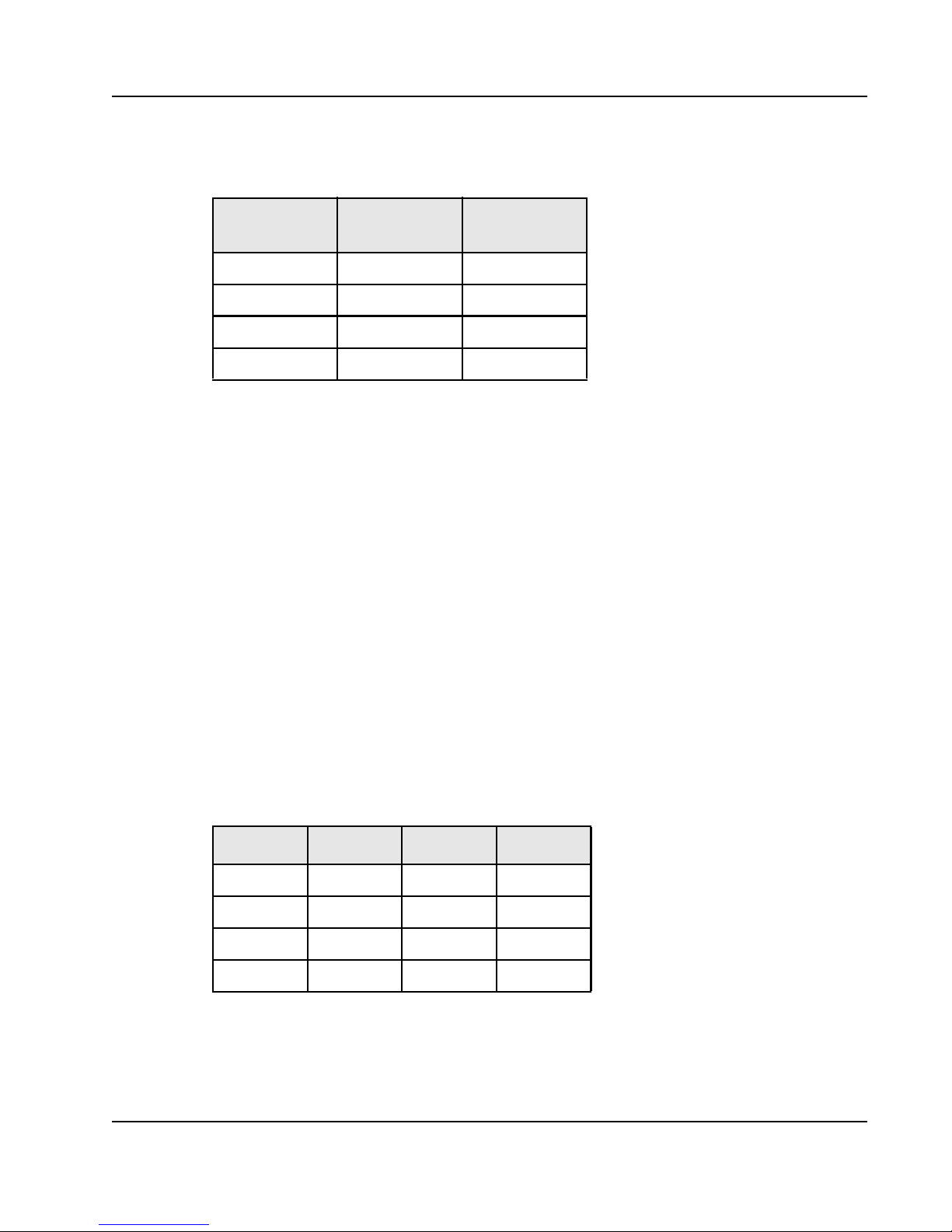
Term Definition
PCIe PCI Express
PCI/X PCI or PCI-X bus mode
SerDes Serial/De-serializer
Revision History
60E1000_MA001_08, Formal, September 2009
This document was rebranded as IDT. It does not include any technical changes.
60E1000_MA001_07, Formal, May 2008
The following changes were made to this version:
• Completed various changes in response to the Tsi384 evaluation board’s removal of support for an
external arbiter (see “Arbitration”).
• Updated the document to support Revision 1.0, Assembly number E1000_AS001_05 of the Tsi384
evaluation board. This assembly version includes the hardware changes listed in the following
table.
Integrated Device Technology
www.idt.com
Tsi384 Evaluation Board User Manual
60E1000_MA001_08
Page 6
About this Document6
Evaluation Board Changes – Assembly E1000_AS001_03
Item Previous Usage/Definition New Usage/Definition
U11/T si384 Bridge Tsi384-133CLVZ Tsi384-133ILVZ2
PCI_LOCKn pull-up None Add 4.7K +/-1K size 0603 resistor
between pin B39 (LOCK#) and pin B41
(3.3V) on J2
3.3Vaux on J2 No connection Short pin A14 (3.3Vaux) to pin A21
(3.3V) by wiring
3.3Vaux on J36 and J37 No connection Short pin A14 (3.3Vaux) to pin A21
(3.3V) by wiring
JTAG signals pull-up 2K pull-up on R288, R293, R294,
R295
PCI reset C231 was 1uF (0603)
(0603ZD105KAT2A)
Change to 10K instead
Changed to 10uF (0603)
MFR P/N: ECJ-1VB0J106M
60E1000_MA001_06, Formal, January 2008
Corrected the descriptions of the S7 and S8 switches. Previously, these descriptions were reversed.
60E1000_MA001_05, Formal, October 2007
Added PCI pull-up resistor values to Table 3.
60E1000_MA001_04, Formal, May 2007
This document supports the Revision 1.0, Assembly number E1000_AS001_03 version of the Tsi384
evaluation board. This assembly version includes the hardware changes listed in the following table.
Evaluation Board Changes – Assembly E1000_AS001_03
Reference Designator Description
Removals
R13 Removed
Add 10 K Ohm pull-down to PCI_RST#
60E1000_MA001_03, Formal, April 2007
This is the general release version of the document. There are no technical differences between this
document and the previous version.
Tsi384 Evaluation Board User Manual
60E1000_MA001_08
Reworks
Integrated Device Technology
www.idt.com
Page 7
About this Document 7
60E1000_MA001_02, Formal, March 2007
This document includes “Bill of Materials” for the Tsi384 evaluation board. It supports the
Revision 1.0, Assembly number E1000_AS001_02 version of the Tsi384 evaluation board. This
assembly version includes the hardware changes listed in the following table.
Evaluation Board Changes – Assembly E1000_AS001_02
Reference Designator Description
Changes
R88 Change to .015ohm
R242,R272,R6 Change to 1Kohm
C182,C183,C193,
C189,C207,C202
R148 Populate
R150 Populate
C77,C45 Install
C235 Change to 300nF
R208 130 Ohm
R215 220 Ohm
R220 441 Ohm
R139 2260 Ohm
R144 220 Ohm
R196 441 Ohm
Removals
R141 Remove
Reworks
Change to 2.2uF
60E1000_MA001_01, Formal, March 2007
This is the first version of the Tsi384 Evaluation Board User Manual. This document supports the
Revision 1.0, Assembly number E1000_AS001_01 version of the Tsi384 evaluation board.
Integrated Device Technology
www.idt.com
Add 1kohm resistor pull-up to LOCK#
Tsi384 Evaluation Board User Manual
60E1000_MA001_08
Page 8

About this Document8
Tsi384 Evaluation Board User Manual
60E1000_MA001_08
Integrated Device Technology
www.idt.com
Page 9

1. Board Design
Topics discussed include the following:
• “Overview” on page 9
• “PCI/X Interface” on page 10
• “PCIe Interface” on page 12
• “Power Management” on page 13
• “Clock Management” on page 16
• “Other Interfaces” on page 18
• “Hardware Reset” on page 18
• “Logic Analyzer Connectivity” on page 18
9
1.1 Overview
The key features of the Tsi384 evaluation board include the following:
• Single x4 lane, 2.5 Gbps PCIe 1.1 compatible riser card (extended height form factor)
• Three PCI/X slots
• 32-/64-bit PCI/X bus, 25–133 MHz operation
• PCI/X power support through system or external supply
• PCIe compliance/debugging test points
Integrated Device Technology
www.idt.com
Tsi384 Evaluation Board User Manual
60E1000_MA001_08
Page 10
Figure 1: Evaluation Board Block Diagram
EEPROM
TSI384
3.3V PCI/X 64bit 133Mhz Edge Connector
R/A Mount Slot 0 (Top)
PCI/X
Power
Management
PCI Express Card Edge X4
PCIe
LA Probe
JTAG
Header
ATX
Connectors
EEPROM
3.3V PCI/X 64bit 133Mhz Edge Connector
Slot 1 (Middle )
PCI/X Isolation Buffer
3.3V PCI/X 64bit 133Mhz Edge Connector
Slot 2 (Lower)
Clock
Management
PCI/X bus
arbiter
1. Board Design10
1.2 PCI/X Interface
1.2.1 Overview
Tsi384 Evaluation Board User Manual
60E1000_MA001_08
The PCI/X Interface is implemented on the board with three slots, in which one is an R/A mounted
connector on the top of the board. All PCI/X connectors are compliant with the PCI/X 2.0b
specification. Appropriate clearance is provided such that up to three PCI/X cards can be inserted for
testing while the board is in an open-chassis standard ATX case.
Integrated Device Technology
www.idt.com
Page 11
1. Board Design 11
The PCI/X Interface supports the configurations listed in Table 1.
Table 1: PCI/X Interface — Supported Configurations
Protocol
PCI 25, 33, 50, 66 3
PCI-X 50, 66 3
PCI-X 100 2
PCI-X 133 1
The support for PCI-X 133 MHz operation is possible with the use of an isolation buffer. The R/A
connector located on the top of board is available in this maximum frequency. The PCI bus is routed
forward and returned to the other slots to expand the bus for multi-slot support.
1.2.2 IDSEL Signals
IDSEL signals are connected in the following order:
• Slot 0 – R/A connector top slot: 2K ohms to AD16 (Device 0)
• Slot 1 – Vertical middle slot: 2K ohms to AD19 (Device 3)
• Slot 2 – Vertical lower slot: 2K ohms to AD18 (Device 2)
The 2K ohm resistor value is consistent with the ability of the Tsi384 to drive the AD lines 2 clock
cycles prior in PCI mode, and 4 clock cycles prior in PCI-X mode. The PCI/X Interface is unterminated
with the exception of the clock signals.
Operating
Speed (MHz)
Number of Slots
Supported
1.2.3 Interrupt Signals
The PCI interrupt signals are connected to the slots as shown in Table 2.
Table 2: PCI Interrupt Routing
Tsi384 Slot 0 Slot 1 Slot 2
AADC
BBAD
CCBA
DDCB
Integrated Device Technology
www.idt.com
Tsi384 Evaluation Board User Manual
60E1000_MA001_08
Page 12
1.2.4 PCI Pull-up Signals
The following signals have a pull-up resistor on the PCI bus.
Table 3: PCI Pull-up Signals
Signal Description Resistor Value
PCI_CBE#[4:7] Byte enables for upper 32-bit AD lines 8.2K
PCI_REQ#[0:3] Bus request 8.2K
PCI_GNT#[0:3] Bus grant 8.2K
PCI_FRAME# Control signal 8.2K
PCI_IRDY#, PCI_TRDY# Control signal 8.2K
PCI_STOP# Control signal 8.2K
PCI_SERR# System error 8.2K
PCI_PERR# Parity error 8.2K
1. Board Design12
PCI_PAR Parity of lower 32-bit lines and CBE bus 8.2K
PCI_PAR64 Parity of upper 32-bit AD lines and CBE bus 8.2K
PCI_DEVSEL# Device select line 8.2K
PCI_INT#[A:D] Interrupt line 2.4K
PCI_PME# PCI Power Management Event occurred 8.2K
1.2.5 Arbitration
The Tsi384 evaluation board has provisions to implement an external arbiter; however, the current PCB
assembly does not have the external arbiter implemented. Therefore, the only valid mode of operati on
is internal arbiter enabled.
1.3 PCIe Interface
The Tsi384 evaluation board implements a four-line PCIe interface. It is designed to connect onto a
PCIe system with a standard x4 finger connector. The system must provide the REFCLK and PERSTN
signals. The PCIe interface has the following design elements:
• Supports Hot insertion and removal
• Mid-bus logic analyzer pads for PCIe RXD/TXD signal probing
• AC coupling on the TXD lanes
• JTAG TDI - TDO loopback for chain continuity
Tsi384 Evaluation Board User Manual
60E1000_MA001_08
Integrated Device Technology
www.idt.com
Page 13
1. Board Design 13
1.4 Power Management
1.4.1 Power Regulation
The evaluation board’s power regulation is implemented as follows:
• Digital 3.3V power supply available from DC/ D C re gu lator or ATX supply
• Digital 1.2V switching regulator
• PCIe supplies filtered using EMI ferrite networks
To support PCI/X cards, the following additional power resources are included:
• 12V to 5V DC/DC converter
• 12V to 3.3V DC/DC converter
• External power connectors – ATX 20-pin connector for supplying all power from an ATX power
supply
1.4.2 Power Requirements
The power requirements and implementation for the Tsi384 is as follows.
Table 4: Tsi384 Power Requirements
Supply Name Symbol Supplied Source
Device Core 1.2V_384 DC/DC switching regulator w/Enable pin
PCIe 1.2V Core 1.2V_A_384 Passive Filter
PCI 3.3v supply 3.3V_384 Power switch w optional Ferrite filter to reduce
PCIe 3.3v supply 3.3V_A_384 Passive Filter
The target power draw of the Tsi384 is a maximum of 2 Watts, all supplies combined. The supplies to
the Tsi384 are controlled during ramp up using enable pins on regulators and switches.
1.4.2.1 PCIe
The PCIe CEM Specification 1.1 defines power limits on PCIe slots according to the number of lanes
available on the card. Power rules regarding x4 PCIe slots are a maximum of 25W slot. Current limits
are included in Table 5.
Table 5: PCIe Connector Current Limits
EMI/noise from PCI environment
Rail Current
3.3V 3A
12V 2.1A
Integrated Device Technology
www.idt.com
Tsi384 Evaluation Board User Manual
60E1000_MA001_08
Page 14

In both cases (x4 or x16), the usage of the 12V supply provides access to the full 25W/75W available
from the system to the board. The PCIe pinout design includes more 12V power pins as it allows more
power-per-pin capability. The evaluation board regulates all power from the 12V system rail; however,
3.3V from the system remains unused.
1.4.2.2 PCI/X
The PCISIG defines the power rules regarding PCI/X cards as a maximum of 25 Watts per card (All
power rails combined power draw). The individual current limits on voltage rails are included in
Table 6.
Table 6: PCI/X Connector current limits
1. Board Design14
Rail Current
3.3v 7.6a
5v 5a
-12v 100ma
12v 500ma
It is not possible “within spec” to provide the full power required to the PCI/X without violating the
specification while drawing power from only a x4 PCIe system. Up to 23W not including regulator
efficiency losses can be made available. The evaluation board provides the power requirements in one
of two ways depending on the application:
• PCIe system power
• ATX System connector
The following conditions summarize the power available for a single PCI/X card without external
supply. An efficiency of 85% is taken into account for switching regulators. These limits can be
exceeded in cases where the system can provide more than the suggested limit, which is usually only
implemented in hot swap systems.
Table 7: PCI/X Connector Current Limit with No External Supply
Rail Supplying Topology Current (Maximum)
3.3V 12V to 3.3V regulator 6A
12V 12V directly 500mA
-12V N/A N/A
5V 12V to 5V regulator 4A
Tsi384 Evaluation Board User Manual
60E1000_MA001_08
Integrated Device Technology
www.idt.com
Page 15

1. Board Design 15
For additional slots, or in cases where the system cannot supply enough power, a separate ATX power
connector is used to power the card. The evaluation board senses the presence of this supply, and
disables the slave PCIe slot power. For the case of a separate external ATX supply, all three slots are
provided with the required power.
1.4.3 Power Sequencing
On power-up, the card power sequencing is as follows:
1. 1.2V powered on
2. PCI/X I/O slot power and pull-ups, and Tsi384 3.3V
12V/-12V/5V PCI are not sequence controlled.
1.4.4 System Power Design
Figure 2 illustrates the power distribution for the riser card. The following list is a functional summary
of the power design:
1. Sequencing control over the following rails:
•3.3V PCI
• 3.3V Tsi384 I/O/PCIe A
• 1.2V Ts i384 Core/PCIe V
VDD
DD
2. ATX 20-pin connector override, which disables all power draw from the PCIe system
3. Current sensing of Tsi384 supplies
Integrated Device Technology
www.idt.com
Tsi384 Evaluation Board User Manual
60E1000_MA001_08
Page 16

Figure 2: System Power Distribution
3v3/5v DC/DC
Regulator
(LM4600)
PCIe
System
12v
ATX
20-pin
-12v
12v
5v
3.3v
Unused
GND
1.2v DC/DC
12V
3.3V
1.2V
Power
Sequencer
3.3v/5v Disable
1.2V PCIE_VDD
3.3V PCIE AVDD
-12V
3.3V I/O
PCI/X
Bus
Connectors
Current
Sense
Current
Sense
Current
Sense
Current
Sense
Tsi384
Electronic/Mech
Breaker w/
Current Limit
1. Board Design16
1.5 Clock Management
1.5.1 PCI/X
Tsi384 Evaluation Board User Manual
60E1000_MA001_08
The Tsi384 requires up to two input clocks to operate:
• 25–133MHz clock for PCI/X
• 100-MHz reference clock for PCIe
The PCI/X and PCIe input clocks are briefly discussed.
The evaluation board supports master and slave clocking for PCI/X.
• Master – When in master mode, the Tsi384 generates the required PCI/X clock for all slots.
• Slave – When in slave mode, an on-board selectable 25–133 MHz clock generator is used as
follows:
Integrated Device Technology
www.idt.com
Page 17

1. Board Design 17
Tip
ICS87604I
PCIe System
PCIe_REFCLK
PCI/X
Bus
Connectors
Tsi384
PCI_CLK
CLKOUT[0:4]
PCI_INT_CLK[0:2,4]
PCI_EXT_CLK[0:3]
Passive Mux
(0r0 RES)
PCI_FBK_CLK
PCI_CLK[0:2]
PLD
ICS557-01
Diff.
SMA
Input
Passive
Mux
(0r0 RES)
ANALOG
MUX
PCIe_SYS_CLK
PCIe_GEN_CLK
PCIe_BERT_CLK
PCIe_REF_CLK
(AC coupled)
Config
— Low skew distribution buffer to all slots and Tsi384
— External clock input for any optional testing
T o multiplex the sources of two clocks, passive resistor muxes are located at the endpoints of
the clock nets. For more information, see the Tsi384 Evaluation Board Schematic
(60E1000_SC002).
1.5.1.1 PCIe
For PCIe clocking, a 100-MHz differential HCSL clock source is required. The clock source is
available in two forms:
• Edge connector clock source – This clock source synchronizes the system SerDes with the Tsi384.
• On-board 100-MHz reference – This clock source can separate the clock domains between the
bridge and the root complex.
The two PCIe clock sources are multiplexed with an analog multiplexer to select between the system
clock or on-board clock (see Figure 3).
1.5.2 System Clock Distribution
Figure 3 shows the distribution of the system clock on the Tsi384 evaluation board.
Figure 3: System Clock Distribution
Integrated Device Technology
www.idt.com
Tsi384 Evaluation Board User Manual
60E1000_MA001_08
Page 18

1.6 Other Interfaces
Tip
PCI Express Edge Connector X4
Reset
Controller
SYS_PCIe_PERSTn
PUSHBUTTON
PCIe_PERSTn
1.6.1 JTAG Interface
To support debug and testing of device, JTAG access to the Tsi384 is available using a standard JTAG
header for Wiggler connection.
1.6.2 EEPROM Interface
A single EEPROM device socket is available for programming registers during startup. The socket is
in an 8-pin DIP format.
1.7 Hardware Reset
Figure 4 illustrates the reset options of the Tsi384 evaluation board.
Figure 4: Board Reset
1. Board Design18
1.8 Logic Analyzer Connectivity
Tsi384 Evaluation Board User Manual
60E1000_MA001_08
Three levels of reset are available:
• Cold reset – This reset is applied during power up. System (card edge) PCIe_PERSTn is muxed
with the board’s reset controller.
• Warm reset – This reset is activated by a push-button reset on the board.
• Hot reset – This reset is activated by the in-band message sent by the root complex. No supporting
hardware is necessary.
For more information on cold, warm, and hot reset levels, see the “Resets, Clocking, and
Initialization Options” chapter in the Tsi384 User Manual.
The serial buses have Midbus pads (TMS818 probe) for visibility of SerDes lines using a
pre-processor. Each probing pad provides access to the RX and TX segments of a x4 link.
T o access the PCI/X bus, a Nexus PCI/X interposer card ca n be used with Tektronix mictor cables. The
card can be plugged into any PCI edge slot, or in-line with the device under test.
Integrated Device Technology
www.idt.com
Page 19

2. Configurable Options
ON
OFF
Topics discussed include the following:
• “Switches” on page 19
• “Shunt Jumpers” on page 26
• “Debug Headers” on page 28
• “Connectors” on page 32
• “LEDs” on page 34
2.1 Switches
2.1.1 DIP Switches
Switches S1 to S6 combine four, small slide switches identified with numbers 1 to 4 (see Table 8 for
individual switch definition).
19
Figure 5: DIP Switch Package/Individual Switch Position
Integrated Device Technology
www.idt.com
Tsi384 Evaluation Board User Manual
60E1000_MA001_08
Page 20

Figure 6: Switch Locations
SW1
S8
S7
S3
S4
S1
S2
S5
S6
SW2
2. Configurable Options20
Tsi384 Evaluation Board User Manual
60E1000_MA001_08
Integrated Device Technology
www.idt.com
Page 21

2. Configurable Options 21
Switch S1 is used to manually set PCI/X bus modes.
Table 8: S1 Settings
Switch
Number
1 PCIXCAP
2 PCIXCAP
3 M66EN
4 PCI_SEL100
Description
setting
setting
setting
setting
Default
Setting
OFF ON = Forces Tsi384’s PCIXCAP input to ground
OFF = Tsi384’s PCIXCAP input has a weak pull up to 3.3V
OFF ON = Tsi384’s PCIXCAP input has a weak pull down to
ground
OFF = Tsi384’s PCIXCAP input has a weak pull up to 3.3V
OFF ON = Forces Tsi384’s M66EN input to ground
OFF = Tsi384’s M66EN input has a weak pull up to 3.3V
ON ON = Forces Tsi384’s PCI_SEL100 input to ground
OFF = Tsi384’s PCI_SEL100 input has a weak pull up to 3.3V
On/Off Setting
Table 9: Bus Mode Setting for S1 (Assumes S2.3 and S2.4 are OFF)
Switch Setting
(Switch 1 - 2 - 3 - 4)
OFF - OFF - x - OFF PCIXCAP = High
Signal Setting Bus Mode
PCIX 100 MHz
M666EN = x
PCI_SEL100 = High
OFF - OFF - x - ON PCIXCAP = High
OFF - ON - x - OFF PCIXCAP = pull-down
OFF - ON - x - ON PCIXCAP = pull-down
ON - x - OFF - OFF PCIXCAP = Low
ON - x - OFF - ON PCIXCAP = Low
Integrated Device Technology
www.idt.com
PCIX 133 MHz
M666EN = x
PCI_SEL100 = Low
PCIX 50 MHz
M666EN = x
PCI_SEL100 = High
PCIX 66 MHz
M666EN = x
PCI_SEL100 = Low
PCI 50 MHz
M666EN = High
PCI_SEL100 = High
PCI 66 MHz
M666EN = High
PCI_SEL100 = Low
Tsi384 Evaluation Board User Manual
60E1000_MA001_08
Page 22

2. Configurable Options22
Table 9: Bus Mode Setting for S1 (Assumes S2.3 and S2.4 are OFF) (Continued)
Switch Setting
(Switch 1 - 2 - 3 - 4)
Signal Setting Bus Mode
ON - x - ON - OFF PCIXCAP = Low
M666EN = Low
PCI_SEL100 = High
ON - x - ON - ON PCIXCAP = Low
M666EN = Low
PCI_SEL100 = Low
Switch S2 is used to connect PCI bus mode signal to the Tsi384.
Table 10: S2 Settings
Switch
Number
1 No function - 2 No function - 3 Bus M66EN
4Bus
Description
connection
PCIXCAP
connection
Default
Setting
ON ON = Connect the PCI M66EN signal to the Tsi384
OFF = Disconnect the PCI M66EN from the Tsi384
ON ON = Connect the PCI PCIXCAP signal to the Tsi384
OFF = Disconnect the PCI PCIXCAP from the Tsi384
PCI 25 MHz
PCI 33 MHz
On/Off Setting
Note that S1 and S2 operate together . When the S2 switches are ON, the S1 setting applies to the whole
bus. For example, when PCIXCAP is connected to the Tsi384 (S2.4 ON), and PCIXCAP is forced to
ground (S1.1 ON), the whole bus will see PCIXCAP low.
Tsi384 Evaluation Board User Manual
60E1000_MA001_08
Integrated Device Technology
www.idt.com
Page 23

2. Configurable Options 23
Switches S3 and S4 are used to set the PCI/X bus external clock frequency. By default the PCI/X bus
clock source is the Tsi384. The external clock can only be connected to the PCI/X bus by replacing
resistors on the board. When an external clock source is used, an on-board PLL is used to set the proper
bus clock frequency. Table 11 contains the clock frequency settings for S3.
Table 11: S3 Settings
Switch
Number
1 DIV_SEL0 OFF [FBDIV_SEL1, FBDIV _SEL0, DIV_SEL1, DIV_SEL0]
2DIV_SEL1OFF
3FBDIV_
4FBDIV_
Description
SEL0
SEL1
Default
Setting
OFF
OFF
On/Off Setting
ON = 1
OFF = 0
0,0,0,0 = x 4
0,0,0,1 = x 3
0,0,1,0 = x 2
0,0,1,1 = x 1
0,1,0,0 = x 5.33
0,1,0,1 = x 4
0,1,1,0 = x 2.667
0,1,1,1 = x 1.33
1,0,0,0 = x 6.667
1,0,0,1= x 5
1,0,1,0= x 3.33
1,0,1,1= x 1.67
1,1,0,0= x 8
1,1,0,1= x 6
1,1,1,0= x 4
1,1,1,1= x 2
Integrated Device Technology
www.idt.com
Tsi384 Evaluation Board User Manual
60E1000_MA001_08
Page 24

Switch S4 controls the external clock PLL.
Table 12: S4 Settings
2. Configurable Options24
Switch
Number
1 PLL Reset ON ON = PLL in reset. PLL clock outputs are low.
2 XTAL select OFF ON = Clock source for PLL is reference clock from connector
3 PLL select OFF ON = PLL is bypassed.
4 No function - -
Description
Default
Setting
On/Off Setting
OFF = PLL is active and clock outputs are enabled.
J10
OFF = Clock source for PLL is a 25-MHz oscillator.
OFF = PLL is enabled. External clock source is multiplied as
per S3 setting
Switch S5 controls the PCIe clock multiplexer and the on-board PCIe reference clock PLL.
Table 13: S5 Settings
Switch
Number
Description
Default
Setting
On/Off Setting
1 No Function - 2PCIe
on-board
PLL enable
3 PCIe clock
multiplexer
enable
4 PCIe clock
source select
ON ON = On-board PCIe reference clock PLL disabled.
OFF = On-board PCIe reference clock PLL enabled.
OFF ON = On-board PCIe clock multiplexer disabled.
OFF = On-board PCIe clock multiplexer enabled.
OFF ON = On-board PCIe reference clock is used.
OFF = System PCIe reference clock is used.
Tsi384 Evaluation Board User Manual
60E1000_MA001_08
Integrated Device Technology
www.idt.com
Page 25

2. Configurable Options 25
Switch S6 configures Tsi384’s power-up options.
Table 14: S6 Settings
Switch
Number
1Clock Master
2 Internal
3 PCI-X clock
4 PCI-X PLL
Description
option
arbiter option
selection
bypass
These switches are not used.
Table 15: S7 and S8 Settings
Default
Setting
OFF ON = Tsi384 is clock slave on the PCI/X bus
OFF = Tsi384 is clock master on the PCI/X bus (clock master
mode)
OFF ON = Internal arbiter is disabled
OFF = Internal arbiter is enabled
ON ON = When in clock master mode, the Tsi384 uses the clock
on PCI_CLK compensated through the PLL to time the
PCI-X Interface.
OFF = When in clock master mode, the Tsi384 uses the
internal clock generated from REFCLK to time the
PCI-X Interface.
OFF ON = PLL is bypassed.
OFF = PLL is enabled.
On/Off Setting
Switch
Number
1 No function - 2 No function - 3 No function - 4 No function - -
2.1.2 Push Button
SW1 is used to turn the ATX power supply ON. This switch is used only when the evaluation board is
powered up with a stand-alone ATX power supply.
SW2 is used to reset the evaluation board. When pushing the reset button, the board is reset the same
way a PCIe system reset would reset the board.
Description
Default
Setting
On/Off Setting
Integrated Device Technology
www.idt.com
Tsi384 Evaluation Board User Manual
60E1000_MA001_08
Page 26

2.2 Shunt Jumpers
J1
J21
J6
Shunt jumpers are used to control special features on the board (see Figure 7). These jumpers are
explained in the following sub-sections.
Figure 7: Shunt Jumper Location
2. Configurable Options26
Tsi384 Evaluation Board User Manual
60E1000_MA001_08
Integrated Device Technology
www.idt.com
Page 27

2. Configurable Options 27
2.2.1 J1 Shunt Jumper
J1 is used to enable the isolation switches on the PCI/X bus. The switches are located between slot 0
and slot 1. The switches are used isolate slot 1 and 2 from the PCI bus in order to reduce loading on slot
0. This allows PCI bus operation at 133 MHz with reduced bus loading.
Table 16: J1 Shunt Jumper Setting
Jumper
Setting
Installed Installed PCI bus Isolation switches are ON. All 3 slots are operational.
Removed PCI bus Isolation switches are OFF. Slot 0 is functional, slot 1 and 2 are
Default
Setting
2.2.2 J6 Shunt Jumper
J6 is used to bypass the On/Off push button to enable the ATX power supply.
Table 17: J6 Shunt Jumper Setting
Jumper
Setting
Installed R emoved Forces ATX power supply ON.
Removed Normal operation, ATX power supply is turned On/OFF from push button.
Default
Setting
2.2.3 J21 Shunt Jumper
J21 is used to force the Tsi384 into a special debug mode. This jumper is not installed.
Function
isolated.
Function
Integrated Device Technology
www.idt.com
Tsi384 Evaluation Board User Manual
60E1000_MA001_08
Page 28

2.3 Debug Headers
J15
J38
J22
J21
Debug headers are used to connect to signals on the board. This section provides header pinouts.
Figure 8: Debug Header Location
2. Configurable Options28
Tsi384 Evaluation Board User Manual
60E1000_MA001_08
Integrated Device Technology
www.idt.com
Page 29

2. Configurable Options 29
1
7
5
9
3
2
4
6
8
10
1
2
3
4
5
6
7
8
9
10
11
12
13
14
15
16
2.3.1 J22 Tsi384 JTAG
Table 18: J22 Pin Assignment
Pin
Number
1TDO
2NC
3TDI
43.3V
5NC
63.3V
7TCK
8NC
9TMS
Signal Assignment J22 Pin Location
10 NC
11 NC
12 GND
13 NC
14 NC
15 NC
16 GND
Integrated Device Technology
www.idt.com
Tsi384 Evaluation Board User Manual
60E1000_MA001_08
Page 30

2.3.2 J23 Logic Analyzer PADs
1
7
5
9
3
2
4
6
8
10
1
2
3
45678910
11
12
131415
1617181920
212223
24
Table 19: J23 Pin Assignment
Pin
Number
1 PCIE_TXD_EDG_P0
2GND
3 PCIE_TXD_EDG_N0
4 PCIE_RXD_EDG_P0
5GND
6 PCIE_RXD_EDG_N0
7 PCIE_TXD_EDG_P1
8GND
9 PCIE_TXD_EDG_N1
Signal Assignment J23 Pin Location
2. Configurable Options30
10 PCIE_RXD_EDG_P1
11 GND
12 PCIE_RXD_EDG_N1
13 PCIE_TXD_EDG_P2
14 GND
15 PCIE_TXD_EDG_N2
16 PCIE_RXD_EDG_P2
17 GND
18 PCIE_RXD_EDG_N2
19 PCIE_TXD_EDG_P3
20 GND
21 PCIE_TXD_EDG_N3
22 PCIE_RXD_EDG_P3
23 GND
24 PCIE_RXD_EDG_N3
Tsi384 Evaluation Board User Manual
60E1000_MA001_08
Integrated Device Technology
www.idt.com
Page 31

2. Configurable Options 31
1
2
3
4
5
6
7
8
9
10
2.3.3 J38 CPLD JTAG
Table 20: J38 Pin Assignment
Pin# Signal Assignment J38 Pin Location
1TCK
2GND
3TDO
43.3V
5TMS
6NC
7NC
8NC
9TDI
10 GND
Integrated Device Technology
www.idt.com
Tsi384 Evaluation Board User Manual
60E1000_MA001_08
Page 32

2.4 Connectors
J2
J3
J36
J37
SLOT0
SLOT1
SLOT2
P1
Figure 9: Board Connector Location
2. Configurable Options32
2.4.1 J2-J36-J37 Connectors
J2, J36, and J37 are used to connect a plug-in card to the T si384’s PCI/X Interface. The connectors’ pin
assignments is as per the PCI standard for 64-bit connectors
Tsi384 Evaluation Board User Manual
60E1000_MA001_08
Integrated Device Technology
www.idt.com
Page 33

2. Configurable Options 33
1
2
3
4
5
6
7
8
9
10
11
12
13
14
15
16
17
18
19
20
2.4.2 J3 ATX Power Connector
A standard ATX power supply can be used to power up the board when used stand alone (not plugged
into a PCIe system).
Table 21: J3 Pin Assignment
Pin
Number
13.3V
23.3V
3GND
45V
5GND
65V
7GND
Signal Assignment J3 Pin Location
8N.C.
95VSB
10 12V
11 3.3V
12 -12V
13 GND
14 GND
15 GND
16 GND
17 GND
18 N.C.
19 5V
20 5V
2.4.3 P1 x4 PCIe Finger Connector
The pin assignment for the finger connector is as per the PCIe standard. Note that the JTAG signals
TDI and TDO are connected together on the board.
Integrated Device Technology
www.idt.com
Tsi384 Evaluation Board User Manual
60E1000_MA001_08
Page 34

2.5 LEDs
D2-D8
D1
D24 D25
D11-D18
D19-D22
Figure 10: LED Location
2. Configurable Options34
Tsi384 Evaluation Board User Manual
60E1000_MA001_08
Integrated Device Technology
www.idt.com
Page 35

2. Configurable Options 35
Table 22: LED Description
LED Designation Signal Assignment Description
D1 BUFSLOT_LED OFF when PCI slots 1 and 2 are isolated
from the bus
D11 PCI33 PCI bus at 33 MHz
D12 PCI25 PCI bus at 25 MHz
D13 PCIX66 PCI-X bus at 66 MHz
D14 PCI66 PCI bus at 66 MHz
D15 PCI50 PCI bus at 50 MHz
D16 PCIX50 PCI-X bus at 50 MHz
D17 PCIX133 PCI-X bus at 133 MHz
D18 PCIX100 PCI-X bus at 100 MHz
D19 PCIe lane 2 valid Valid PCIe connection on lane 2
D2 -12V ON when -12V rail is active
D20 PCIe lane 0 valid Valid PCIe connection on lane 0
D21 PCIe lane 3 valid Valid PCIe connection on lane 3
D22 PCIe lane 1 valid Valid PCIe connection on lane 1
D3 3.3V_384 ON when Tsi384 3.3V rail is active
D4 5V ON when 5V rail is active
D5 5VSB ON when 5V standby rail is active
D6 3.3V ON when 3.3V rail is active
D7 12V ON when 12V rail is active
D8 3.3V_PCI ON when 3.3V rail on the PCI bus
is active
D24 External arbiter ON when external PCI/X arbiter is active
D25 External arbiter ON when in PCI/X mode
Integrated Device Technology
www.idt.com
Tsi384 Evaluation Board User Manual
60E1000_MA001_08
Page 36

2. Configurable Options36
Tsi384 Evaluation Board User Manual
60E1000_MA001_08
Integrated Device Technology
www.idt.com
Page 37

3. Bill of Materials
The bill of materials (BOM) for the Tsi384 evaluation board is listed in the following table.
Table 23: Bill of Materials
Quantity Reference Designator Part Number Manufacturer Package Type Description
37
1 AP_U1 115-13-308-41-001 MILL-MAX 115-13-308-41-001 DUAL-IN-LINE SOCKET, 0.1IN,
12 C1,C4,C9, C16, C22,
C26-30, C143,C165
7 C2-3,C5,C7,C11,
C14,C31
26 C6, C8, C12-13, C15,
C39, C59, C73, C80,
C92-94, C96,C98, C102,
C106-107, C128-129,
C172-173, C177, C234,
C240-242
5 C10, C62, C140, C162,
C175
113 C17-21, C23-25, C38,
C48-49, C52, C60-61,
C64-71, C105, C108-127,
C130-139, C141-142,
C144-161, C163-164,
C166-171, C176,C179,
C184-186, C190,C192,
C194-196, C198,
C200-201, C203, C206,
C211-212, C217-218,
C220-223, C226-228,
C233, C245-249
7 C32, C35-37, C46,C76,
C90
4 C33-34, C53-54 04025A180JAT2A AVX CAPC0402 NP0 CER SMT, 18PF, 5%, 16V,
4 C42,C87, C91,C100 TAJA106K016R AVX CAPT3216-18 TANT SMT , 10UF, 10%, 16V,
6 C43-44, C74-75, C89,
C101
2 C45,C77 12103C105KAT2A AVX CAPC1210 X7R CER SMT, 0.22UF, 10%, 50V,
8 C47,C51, C55-56,
C78-79, C81-82
6 C50,C178, C197,C199,
C225,C231
2 C85,C99 ECJ-0EB1C104K PANASONIC CAPC0402 X5R CER SMT, 100NF, 10%, 16V,
1206ZD106KAT2A AVX CAPC1206 X5R CER SMT, 10UF, 10%, 10V,
TAJC476K016R AVX CAPT6032-28 TANT SMT, 47UF, 10%, 16V,
06033D104KAT2A AVX CAPC0603 X5R CER SMT, 0.1UF, 10%, 25V,
0402ZC103KAT2A AVX CAPC0402 X7R CER SMT, 0.01UF, 10%, 10V,
0402ZD104KAT2A AVX CAPC0402 X5R CER SMT, 0.1UF, 10%, 10V,
EEVFC1E101P PANASONIC CAPAE95W62H ALUM ELEC SMT, 100UF, 20%,
ECJ-4YB1E226M PANASONIC CAPC1210 X5R CER SMT, 22UF, 20%, 25V,
12106D107MAT2A
0603ZD105KAT2A A VX CAPC0603 X5R CER SMT, 1UF, 10%, 10V,
AVX CAPC1210 X5R CER SMT, 100UF, 20%, 6.3V,
8PIN
1206
6032-28
0603
0402
0402
25V
0402
3216-18
1210
CAPC1210
1210
0603
CAPC0402
Integrated Device Technology
www.idt.com
Tsi384 Evaluation Board User Manual
60E1000_MA001_08
Page 38

3. Bill of Materials38
Table 23: Bill of Materials (Continued)
Quantity Reference Designator Part Number Manufacturer Package Type Description
1 C95 ECJ-2VB1H103K PANASONIC CAPC0805 X7R CER SMT, 10NF, 10%, 50V,
1 C97 0402ZC103JAT2A AVX CAPC0402 X7R CER SMT, 0.01UF, 5%, 10V,
1 C174 ECJ-1VB0J106M PANASONIC CAPC0603 X5R CER SMT, 10UF, 20%, 6.3V,
1 C181 ECJ-1VB0J106M PANASONIC CAPC0603 X5R CER SMT, 10UF, 20%, 6.3V,
7 C182-183, C189,C191,
C193,C202, C207
2 C250-251 0402YC101KAT2A AVX CAPC0402 X7R CER SMT , 100PF , 10%, 16V,
20 D1-8, D11-22 HSMG-C150 AGILENT LED_HSMG-C150 GREEN LED, UNTINTED,
1 D9 DIODES INC. DIOSMA 2A SCHOTTKY DIODE
1 D10 S1B FAIRCHILD DIOSMA GENERAL PURPOSE
1 D23 LCDA15C-1.TC SEMTECH SOT143 TVS DIODE ARRAY
2 D24-25 HSMG-C150 AGILENT LED_HSMG-C150 GREEN LED, UNTINTED,
1 F1 R154 010 LITTLEFUSE FUSE_154 SMT FUSE BLOCK FOR FAST
4 FB1-2,FB4, FB7 BLM18AG601SN1
2 FB3,FB6 BLM31PG500SN1
2 J1,J6 69190-102 FCI 69190-102H 2X1, 0.1IN HDR
1 J2 MERITEC 981131-184-2MPF 64-BIT PCI/X CONNECTOR 3.3V
1 J3 39-30-0200 MOLEX 39-30-0200 R/A A TX PWR JACK, 0.165"
1 J21 69190-102 FCI 69190-102H 2X1, 0.1IN HDR
1 J22 5103309-3 TYCO 5103309-3 2X8, 0.1IN HDR,CENTER/DUAL
2 J36-37 145165-4 AMP 145165-4 PCI MOTHERBOARD, 64BIT,
1 J38 67997-110 FCI 67997-110H 2X5, 0.1IN HDR
1 L1 COILCRAFT LPS4018 2.2UH SMT POWER INDUCTOR,
1 P1 X4PCIE_FINGER_
MURATA CAPC0402 X5R CER SMT, 2.2UF, 20% 6.3V
D
B
CONNECTOR
MURATA FB_0603 SMT FERRITE BEAD, 60OHMS,
MURATA FB_1206 SMT FERRITE BEAD, 50OHMS,
IDT X4PCIE_FINGER_
CONNECTOR
0805 CAP C 0805
0402
0603
0603
CAPC0402
0402
DIFFUSED
RECT IFIE R 0. 5 VF
RECTIFIER
DIFFUSED
10 A F US E ( IN CL U D E D )
25%, 0.2AM P S, 0 6 03
25%, 3AMPS, 1206
R/A W /CL I PS, 0 .1M I L
PI T C H , M I N I FI T W/ P E G S
P O L A R I Z I N G B A R S H R O U D
3.3V, THRU
2.5A I S AT, .070E S R
PCIE X4 FINGER CONNECTOR
Tsi384 Evaluation Board User Manual
60E1000_MA001_08
Integrated Device Technology
www.idt.com
Page 39

3. Bill of Materials 39
Table 23: Bill of Materials (Continued)
Quantity Reference Designator Part Number Manufacturer Package Type Description
2 Q1-2 2N7002 FAIRCHILD SOT23-3-GSD N-CHANNEL MOSFET
1 Q3 FDS6990A FAIRCHILD SOIC127P6-8 2N-CH MOSFET 30V 7.5A
2 Q4-5 IRF8915 INTERNATIONAL
18 R1, R174-175, R260,
R263, R266, R275-282,
R289-292
22 R2-5,R7-8, R51,R77,
R217,R227, R245-253,
R257-258, R267
3 R6,R244, R272 ERJ-3EKF1001V PANASONIC RESC0603 RES SMT, 1K OHM, 0.1W, 1%,
5 R9-12,R209 ERJ-3GEYJ242V PANASONIC RESC0603 RES SMT, 2.4K OHM, 0.1W, 5%,
21 R13,R52, R54,R83,
R86-87, R91,R93,
R95,R100, R114-117,
R136,R151, R172-173,
R240,R259, R264
67 R14-45, R55-73,
R82,R85, R118,R120,
R137,R146, R152,R157,
R187,R198, R207,R226,
R241-242, R256,R283
9 R46-48, R76,R80,
R92,R210, R243,R274
8 R49,R148, R150,R158,
R288, R293-295
4 R50,R74, R214,R265 ERJ-3GEYJ201V PANASONIC RESC0603 RES SMT, 200 OHM, 0.1W, 5%,
2 R53,R273 ERJ-3GEYJ563V PANASONIC RESC0603 RES SMT, 56K OHM, 0.1W, 5%,
2 R75,R236 PANASONIC RESC0402 RES SMT , 10 OHM, 0.0625W, 5%,
11 R78-79, R81,R84, R178,
R284-287, R296, R299
3 R88,R213, R238 VISHAY RESC2010 RES SMT , 0.015 OHM, 0.5W, 1%,
2 R89,R224 ERJ-3EKF1502V PANASONIC RESC0603 RES SMT, 15.0K OHM, 0.1W, 1%,
1 R90 ERJ-3EKF1372V PANASONIC RESC0603 RES SMT, 13.7K OHM, 0.1W, 1%,
14 R102,R149, R181,
R199-206, R255,R268,
R270
ERJ-3EKF3920V PANASONIC RESC0603 RES SMT, 392 OHM, 0.1W, 1%,
ERJ-3GEYJ512V PANASONIC RESC0603 RES SMT, 5.1K OHM, 0.1W, 5%,
ERJ-3EKF1001V PANASONIC RESC0603 RES SMT, 1K OHM, 0.1W, 1%,
ERJ-3GEYJ822V PANASONIC RESC0603 RES SMT, 8.2K OHM, 0.1W, 5%,
ERJ-3GEYJ103V PANASONIC RESC0603 RES SMT, 10K OHM, 0.1W, 5%,
ERJ-3GEYJ202V PANASONIC RESC0603 RES SMT, 2K OHM, 0.1W, 5%,
PANASONIC RESC0402 RES SMT, 33.2 OHM, 0.0625W,
ERJ-2GE0R00X PANASONIC RESC0402 RES SMT, 0 OHM, 0.063W, 5%,
RECTIFIER
S O I C 1 2 7 P 6 - 8 2 N - C H M O S F E T 2 0 V 8 . 9 A
0603
0603
0603
0603
0603
0603
0603
0603
0603
0603
0402
1%, 0402
2010, CURRENT SENSE
0603
0603
0402
Integrated Device Technology
www.idt.com
Tsi384 Evaluation Board User Manual
60E1000_MA001_08
Page 40

3. Bill of Materials40
Table 23: Bill of Materials (Continued)
Quantity Reference Designator Part Number Manufacturer Package Type Description
4 R104, R107-109 ERJ-2RKF49R9X PANASONIC RESC0402 RES SMT, 49.9 OHM, 0.063W,
4 R105-106, R111-112 PANASONIC RESC0402 RES SMT, 33.2 OHM, 0.0625W,
5 R113,R1 19, R124,R128,
R262
1 R121 ERJ-3GEYJ473V PANASONIC RESC0603 RES SMT, 47K OHM, 0.1W, 5%,
2 R122,R138 VISHAY RESC2010 RES SMT, 0.100 OHM, 0.5W, 1%,
1 R132 ERJ-3EKF7151V PANASONIC RESC0603 RES SMT, 7.15K OHM, 0.1W, 1%,
1 R142 ERJ-3EKF1502V PANASONIC RESC0603 RES SMT, 15.0K OHM, 0.1W, 1%,
3 R176-177, R179 ERJ-3GEYJ103V P ANASONIC RESC0603 RES SMT , 10K OHM, 0.1W, 5%,
2 R221,R230 ERJ-3EKF1103V PANASONIC RESC0603 RES SMT, 110K OHM, 0.1W, 1%,
2 R222,R229 ERJ-2RKF1000X PANASONIC RESC0402 RES SMT, 100 OHM, .06W, 1%,
2 R223,R225 9C06031A0R00JL
1 R228 ERJ-3GEYJ223V PANASONIC RESC0603 RES SMT, 22K OHM, 0.1W, 5%,
2 R231-232 ERJ-8GEY0R00V PANASONIC RESC1206 RES SMT, 0 OHM, 0.25W, 5%,
1 R233 ERJ-3GEYJ512V PANASONIC RESC0603 RES SMT, 5.1K OHM, 0.1W, 5%,
1 R235 PANASONIC RESC0603 RES SMT, 10K OHM, 0.1W, 1%,
1 R237 9C06031A0R00JL
1 R261 ERJ-3GEYJ471V PANASONIC RESC0603 RES SMT, 470 OHM, 0.1W, 5%
8 S1-8 1-1435790-4 TYCO SW_1-1435790-4 DIPSWITCH, 4 SWITCHES
1 SW1 PTS125SM43 ITT/CANNON PTS125 PUSHBUTTON SWITCH, 0.5 X
1 SW2 EVQPAC07K PANASONIC SW_EVQPAC07K P U S H B U T T O N S W I T C H
6 TP1-6 TESTPOINT
1 U1 MM74HC74AM FAIRCHILD SOIC127P6-14 DUAL D-TYPE FLIP-FLOP WITH
3 U2-3,U32 LMC7221BIM5 NATIONAL SOT23-5 CMOS COMPARATOR, R-TO-R
PA NASONIC RESC0603 RES SM T, 475 OH M, 0.1W, 1% ,
YAGEO RESC0603 RES SMT, 0 OHM, 0.1W, 5%,
HFT
YAGEO RESC0603 RES SMT, 0 OHM, 0.1W, 5%,
HFT
1%, 0402
1%, 0402
0603
0603
2010, CURRENT SENSE
0603
0603
0603
0603
0402
0603
0603
1206
0603
0603
0603
0603
0.5
PRE S ET AND CLE AR
I N P U T, O P E N D R A I N O U T P U T
Tsi384 Evaluation Board User Manual
60E1000_MA001_08
Integrated Device Technology
www.idt.com
Page 41

3. Bill of Materials 41
Table 23: Bill of Materials (Continued)
Quantity Reference Designator Part Number Manufacturer Package Type Description
2 U4-5 SN74LVC1G14DB
VT
1 U6 ICS87604AGI IDT TSOP65P81-28 LOW VOLTAGE, LOW SKEW 1:4
1 U7 SN74LVC139AD TI SOIC127P6-16 DUAL 2-LINE TO 4-LINE
2 U9,U22 LINEAR LTM4600EV_PBF 10A 4.5V TO 20V INPUT, 0.6V TO
1 U10 ICS557M-01 ICS SOIC127P6-8 100MHZ, HCSL OUT, 3.3V,
1 U11 TSI384-133ILVZ2 IDT BGA100P16X16-2
1 U12 ICS557G-08 IDT TSSOP65P64-16 2:1 MULTIPLEXER CHIP FOR
1 U15 TL7702BCD TI SOIC127P6-8 POR GENERATOR, 3.5-18V VCC
2 U16,U18 NC7SZ08M5X FAIRCHILD SOT23-5 TINY LOGIC 2-INPUT AND GATE
1 U26 LM4050_IM3-2.5 MAXIM SOT23-3 SHUNT REFERENCE VOLTAGE
1 U29 LTC4210-2CS6 LINEAR TSOT23-6 HOT SWAP CONTROLLER
1 U33 INTERSIL TS S O P 5 0 P 4 9 - 1 0 M O N O L I T HI C 2 A S T E P D O W N
3 U34-36 QS34XVH245Q3 IDT QVSOP-80 32-BIT FET BUS SWITCH
1 U37 EPM240T100C3 ALTERA VQFP50P16X16-1
2 Y1-2 HCM4925.000MA
BJT
TI SOT23-5 SINGLE SCHMITT-TRIGGER
56
00
CITIZEN XTAL_HCM4925_
000MABJT
INVERTER
PCI/PCI-X ZERO DELAY CLOCK
GENERATOR
D E C O D E R / M U L T I P L E X E R
5.0V OUTPUT SWITCHING
REGULATOR
25MHZ INPUT (SUPPORTS
PCIE)
FORWARD MODE PCI EXPRESS
TO PCI/ X BRIDGE
PCI EXPRESS
1.65 V TO 5.5V
2.5V
REGULATOR, 1.5MHZ, 2.6-5V IN,
0.8 TO VIN OUT
C P L D , 2 4 0 M A C R O C E L L
25MHZ CRYSTAL, 18PF, 30PPM
C A L . T O L . , 5 0 P P M T E M P. T O L .
Integrated Device Technology
www.idt.com
Tsi384 Evaluation Board User Manual
60E1000_MA001_08
Page 42

3. Bill of Materials42
Tsi384 Evaluation Board User Manual
60E1000_MA001_08
Integrated Device Technology
www.idt.com
Page 43

CORPORATE HEADQUARTERS
6024 Silver Creek Valley Road
San Jose, CA 95138
DISCLAIMER Integrated Device Techno l ogy, Inc. (IDT) and its subsidiaries reserve the right to mo di fy th e p ro du cts an d/or specifications described herein at any time an d a t ID T’s sol e di scr etion . A ll i nf or m ation i n th is do cum en t, incl u ding de scri p ti on s of
product features and performance, is subject to change without notice. Performance specifications and the operating parameters of the described products are determined in the independe nt sta t e a nd a re not gua ra nte ed to pe rfo r m th e sam e w ay whe n
installed in customer products. The in format ion co ntaine d her ein is prov ided wit hout re prese ntat ion or warrant y of any kin d, wh ether expr ess or implied , includ ing, but not limi ted to, the suitab ility of IDT’s products for any particu lar purp ose, an impli ed
warranty of merchantability, or non-infringement of the intellectual property rights of others. This document is presented only as a guide and does not convey any license under intellectual property rights of IDT or any third parties.
IDT’s products are not intended for use in life support systems or similar devices where the failure or malfunction of an IDT product can be reasonably expected to significantly affect the health or safety of users. Anyone using an IDT product in such a
manner does so at their own risk, absent an express, written agreement by IDT.
Integrated Device Technology, IDT and the IDT logo are registered trademarks of IDT. Other trademarks and service marks used herein, including protected names, logos and designs, are the property of IDT or their respective third party owners.
Copyright 2009. All rights reserved.
2009 Integrated Device Technology, Inc *Notice: The information in this document is subject to change without notice
for SALES:
800-345-7015 or 408-284-8200
fax: 408-284-2775
www.idt.com
for Tech Support:
email: ssdhelp@idt.com
phone: 408-284-8208
Document: 60E1000_MA001_08
September 2009
 Loading...