

Page 1

IDT
Tsi620 Evaluation Board
User Manual
60D7000_MA001_03
August 7, 2009
6024 Silver Creek Valley Road San Jose, California 95138
Telephone: (408) 284-8200 • FAX: (408) 284-3572
Printed in U.S.A.
©2009 Integrated Device Technology, Inc.
Page 2

Integrated Device Technology, Inc. ("IDT") reserves the right to make changes to its products or specifications at any time, without notice, in order to improve design or
performance. IDT does not assume responsibility for use of any circuitry described herein other than the circuitry embodied in an IDT product. Disclosure of the information
herein does not convey a license or any other right, by implication or otherwise, in any patent, trademark, or other intellectual property right of IDT. IDT products may
contain errata which can affect product performance to a minor or immaterial degree. Current characterized errata will be made available upon request. Items identified
herein as "reserved" or "undefined" are reserved for future definition. IDT does not assume responsibility for conflicts or incompatibilities arising from the future definition
of such items. IDT products have not been designed, tested, or manufactured for use in, and thus are not warranted for, applications where the failure, malfunction, or
any inaccuracy in the application carries a risk of death, serious bodily injury, or damage to tangible property. Code examples provided herein by IDT are for illustrative
purposes only and should not be relied upon for developing applications. Any use of such code examples shall be at the user's sole risk.
Copyright © 2009 Integrated Device Technology, Inc.
All Rights Reserved.
The IDT logo is registered to Integrated Device Technology, Inc. IDT and CPS are trademarks of Integrated Device
Technology, Inc.
.
“Accelerated Thinking” is a service mark of Integrated Device Technology, Inc.
GENERAL DISCLAIMER
Page 3

Contents
1. Board Hardware . . . . . . . . . . . . . . . . . . . . . . . . . . . . . . . . . . . . . . . . . . . . . . . . . . . . . 7
1.1 Overview . . . . . . . . . . . . . . . . . . . . . . . . . . . . . . . . . . . . . . . . . . . . . . . . . . . . . . . . . . . . . . . . . . . . . . . . . . . . . . . . . 7
1.2 Board Architecture . . . . . . . . . . . . . . . . . . . . . . . . . . . . . . . . . . . . . . . . . . . . . . . . . . . . . . . . . . . . . . . . . . . . . . . . . . 7
1.2.1 Baseband Processing Data Flow . . . . . . . . . . . . . . . . . . . . . . . . . . . . . . . . . . . . . . . . . . . . . . . . . . . . . . . 7
1.2.2 Board Specification . . . . . . . . . . . . . . . . . . . . . . . . . . . . . . . . . . . . . . . . . . . . . . . . . . . . . . . . . . . . . . . . . 9
1.2.3 Board Architecture . . . . . . . . . . . . . . . . . . . . . . . . . . . . . . . . . . . . . . . . . . . . . . . . . . . . . . . . . . . . . . . . . 11
1.3 Board Hardware Functional Description . . . . . . . . . . . . . . . . . . . . . . . . . . . . . . . . . . . . . . . . . . . . . . . . . . . . . . . . 12
1.3.1 sRIO Switching and PrPMC Module. . . . . . . . . . . . . . . . . . . . . . . . . . . . . . . . . . . . . . . . . . . . . . . . . . . 12
1.3.2 FPGA Block. . . . . . . . . . . . . . . . . . . . . . . . . . . . . . . . . . . . . . . . . . . . . . . . . . . . . . . . . . . . . . . . . . . . . . 17
1.3.3 DSP Block . . . . . . . . . . . . . . . . . . . . . . . . . . . . . . . . . . . . . . . . . . . . . . . . . . . . . . . . . . . . . . . . . . . . . . . 19
1.3.4 System Management Controller. . . . . . . . . . . . . . . . . . . . . . . . . . . . . . . . . . . . . . . . . . . . . . . . . . . . . . . 22
1.3.5 Clocking Management . . . . . . . . . . . . . . . . . . . . . . . . . . . . . . . . . . . . . . . . . . . . . . . . . . . . . . . . . . . . . . 24
1.3.6 Power Management . . . . . . . . . . . . . . . . . . . . . . . . . . . . . . . . . . . . . . . . . . . . . . . . . . . . . . . . . . . . . . . . 26
1.3.7 JTAG Port and I2C Bus . . . . . . . . . . . . . . . . . . . . . . . . . . . . . . . . . . . . . . . . . . . . . . . . . . . . . . . . . . . . . 29
1.4 PCB Characteristics . . . . . . . . . . . . . . . . . . . . . . . . . . . . . . . . . . . . . . . . . . . . . . . . . . . . . . . . . . . . . . . . . . . . . . . . 30
1.4.1 PCB Form Factor . . . . . . . . . . . . . . . . . . . . . . . . . . . . . . . . . . . . . . . . . . . . . . . . . . . . . . . . . . . . . . . . . . 30
1.5 Configuration Options . . . . . . . . . . . . . . . . . . . . . . . . . . . . . . . . . . . . . . . . . . . . . . . . . . . . . . . . . . . . . . . . . . . . . . 31
1.5.1 DIP Switches . . . . . . . . . . . . . . . . . . . . . . . . . . . . . . . . . . . . . . . . . . . . . . . . . . . . . . . . . . . . . . . . . . . . . 31
1.5.2 Jumpers . . . . . . . . . . . . . . . . . . . . . . . . . . . . . . . . . . . . . . . . . . . . . . . . . . . . . . . . . . . . . . . . . . . . . . . . . 34
1.5.3 Push Button and Toggle Switch . . . . . . . . . . . . . . . . . . . . . . . . . . . . . . . . . . . . . . . . . . . . . . . . . . . . . . . 34
1.6 Board Connectors . . . . . . . . . . . . . . . . . . . . . . . . . . . . . . . . . . . . . . . . . . . . . . . . . . . . . . . . . . . . . . . . . . . . . . . . . 36
1.6.1 JTAG and FPGA Programming Connectors . . . . . . . . . . . . . . . . . . . . . . . . . . . . . . . . . . . . . . . . . . . . . 36
1.6.2 Communication Interface Connectors . . . . . . . . . . . . . . . . . . . . . . . . . . . . . . . . . . . . . . . . . . . . . . . . . . 36
1.6.3 SMA Connectors . . . . . . . . . . . . . . . . . . . . . . . . . . . . . . . . . . . . . . . . . . . . . . . . . . . . . . . . . . . . . . . . . . 37
1.6.4 MISC Connectors. . . . . . . . . . . . . . . . . . . . . . . . . . . . . . . . . . . . . . . . . . . . . . . . . . . . . . . . . . . . . . . . . . 37
1.7 LEDs and Display . . . . . . . . . . . . . . . . . . . . . . . . . . . . . . . . . . . . . . . . . . . . . . . . . . . . . . . . . . . . . . . . . . . . . . . . . 37
1.7.1 Power Good Indicators. . . . . . . . . . . . . . . . . . . . . . . . . . . . . . . . . . . . . . . . . . . . . . . . . . . . . . . . . . . . . . 39
1.7.2 AMC MMC LEDs . . . . . . . . . . . . . . . . . . . . . . . . . . . . . . . . . . . . . . . . . . . . . . . . . . . . . . . . . . . . . . . . . 39
1.7.3 LED Display. . . . . . . . . . . . . . . . . . . . . . . . . . . . . . . . . . . . . . . . . . . . . . . . . . . . . . . . . . . . . . . . . . . . . . 39
1.7.4 Tri-color LEDs. . . . . . . . . . . . . . . . . . . . . . . . . . . . . . . . . . . . . . . . . . . . . . . . . . . . . . . . . . . . . . . . . . . . 39
1.7.5 SFP Optical Transceiver LEDs . . . . . . . . . . . . . . . . . . . . . . . . . . . . . . . . . . . . . . . . . . . . . . . . . . . . . . . 40
1.7.6 GPIO LEDs . . . . . . . . . . . . . . . . . . . . . . . . . . . . . . . . . . . . . . . . . . . . . . . . . . . . . . . . . . . . . . . . . . . . . . 40
3
2. Board Software. . . . . . . . . . . . . . . . . . . . . . . . . . . . . . . . . . . . . . . . . . . . . . . . . . . . . 41
2.1 PMC Software . . . . . . . . . . . . . . . . . . . . . . . . . . . . . . . . . . . . . . . . . . . . . . . . . . . . . . . . . . . . . . . . . . . . . . . . . . . . 41
2.1.1 Running the Software Using Ramdisk. . . . . . . . . . . . . . . . . . . . . . . . . . . . . . . . . . . . . . . . . . . . . . . . . . 42
2.1.2 Running the Software Using NFS Server . . . . . . . . . . . . . . . . . . . . . . . . . . . . . . . . . . . . . . . . . . . . . . . 43
2.1.3 Installing the PMC Software . . . . . . . . . . . . . . . . . . . . . . . . . . . . . . . . . . . . . . . . . . . . . . . . . . . . . . . . . 44
2.1.4 Modifying the PMC Software . . . . . . . . . . . . . . . . . . . . . . . . . . . . . . . . . . . . . . . . . . . . . . . . . . . . . . . . 44
2.2 FPGA Software . . . . . . . . . . . . . . . . . . . . . . . . . . . . . . . . . . . . . . . . . . . . . . . . . . . . . . . . . . . . . . . . . . . . . . . . . . . 45
2.2.1 Installing the FPGA Software . . . . . . . . . . . . . . . . . . . . . . . . . . . . . . . . . . . . . . . . . . . . . . . . . . . . . . . . 46
2.2.2 Running the FPGA Software . . . . . . . . . . . . . . . . . . . . . . . . . . . . . . . . . . . . . . . . . . . . . . . . . . . . . . . . . 48
Intergrated Device Technology
www.idt.com
Tsi620 Evaluation Board User Manual
60D7000_MA001_03
Page 4

4
2.2.3 FPGA Hardware Load Facilities . . . . . . . . . . . . . . . . . . . . . . . . . . . . . . . . . . . . . . . . . . . . . . . . . . . . . . 49
2.2.4 Software Environment. . . . . . . . . . . . . . . . . . . . . . . . . . . . . . . . . . . . . . . . . . . . . . . . . . . . . . . . . . . . . . 50
2.3 DSP Software. . . . . . . . . . . . . . . . . . . . . . . . . . . . . . . . . . . . . . . . . . . . . . . . . . . . . . . . . . . . . . . . . . . . . . . . . . . . . 51
2.3.1 Installing the DSP Software. . . . . . . . . . . . . . . . . . . . . . . . . . . . . . . . . . . . . . . . . . . . . . . . . . . . . . . . . . 51
2.3.2 Running the DSP Software . . . . . . . . . . . . . . . . . . . . . . . . . . . . . . . . . . . . . . . . . . . . . . . . . . . . . . . . . . 52
2.3.3 DSP Hardware Facilities . . . . . . . . . . . . . . . . . . . . . . . . . . . . . . . . . . . . . . . . . . . . . . . . . . . . . . . . . . . . 52
2.4 PMC/DSP/FPGA Software Execution. . . . . . . . . . . . . . . . . . . . . . . . . . . . . . . . . . . . . . . . . . . . . . . . . . . . . . . . . . 53
Tsi620 Evaluation Board User Manual
60D7000_MA001_03
Intergrated Device Technology
www.idt.com
Page 5

About this Document
This document discusses the functional characteristics of the Tsi620 evaluation board. It describes the
board’s key specifications, system architecture, and hardware implementation approaches. In addition,
it discusses the board’s configuration options, connectors, and LEDs.
The next version of this document will explain how the board’s software can be used to test the board’s
PMC, FPGA, and DSP capabilities.
Terms
AIF Antenna Interface
AMC Advanced Mezzanine Card
BB Baseband
5
bps Bit per second
BW Bandwidth (Usually means row data including encryption and service)
CPRI Common Public Radio Interface
DDR2 Double Data Rate 2 SDRAM
DFT Design for Testing
DSP Digital Signal Processor
EVB Evaluation Board
H/W Hardware
I/F Interface
LE Logic Element (FPGA programmable logic unit)
MMC MicroTCA AMC module management controller
OBSAI Open Base Station Air Interface
RF Radio Frequency
S/W Software
SFP Small Form Factor Pluggable
SPI Serial Peripheral Interface
SRIO Serial RapidIO
PrPMC Processor PMC
Intergrated Device Technology
www.idt.com
Tsi620 Evaluation Board User Manual
60D7000_MA001_03
Page 6

6
Revision History
60D7000_MA001_03, Formal, August 2009
There are no technical changes to this document.
60D7000_MA001_02, Formal, November 2008
This version was updated to include information about the software on the Tsi620 evaluation board
(see “Board Software”).
60D7000_MA001_01, Preliminary, June 2008
This is the first version of the Tsi620 Evaluation Board Manual.
Tsi620 Evaluation Board User Manual
60D7000_MA001_03
Intergrated Device Technology
www.idt.com
Page 7

1. Board Hardware
This section discusses the following topics:
• “Overview” on page 7
• “Board Architecture” on page 7
• “Board Hardware Functional Description” on page 12
• “PCB Characteristics” on page 30
• “Configuration Options” on page 31
1.1 Overview
This chapter discusses the functional characteristics of the Tsi620 evaluation board. It describes the
board’s key specifications, system architecture, and hardware implementation approaches.
7
The Tsi620 evaluation board serves the following purposes:
• To demonstrate the Tsi620’s potential application in a typical wireless baseband processing system
• To provide a hardware platform for customers to assess the Tsi620’s major features and to evaluate
the performance of the device in a real wireless base station system
• To function as a design reference for customer’s Tsi620 hardware development
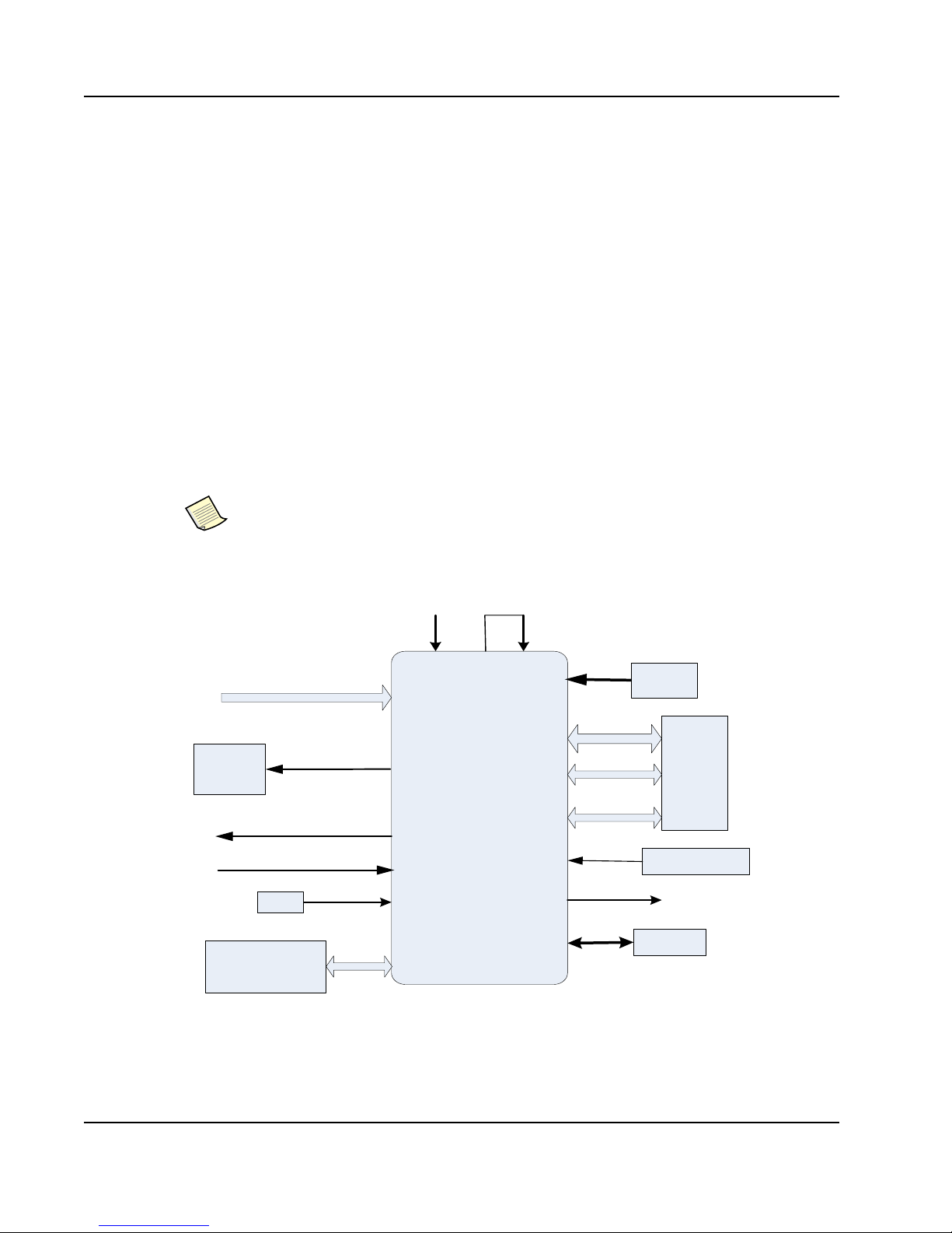
1.2 Board Architecture
1.2.1 Baseband Processing Data Flow
The Tsi620 evaluation board can function as a baseband processing module in a wireless base station
application. The board can connect to an RF module with OBSAI/CPRI links. It is assumed that the
board will be functioning in an MicroTCA chassis with AMC-sRIO backplane, which provides
networking and system management interconnection.
Intergrated Device Technology
www.idt.com
Tsi620 Evaluation Board User Manual
60D7000_MA001_03
Page 8

8
AMC Finger Connector
Tsi620
SRIO Swi tch
SFP
Cage
SFP
Cage
TCI6488
DSP
BB Processing
Stratix3
FPGA
BB Processing
PrPMC Connector
AMC Vertical Connector
DDR2 256MB
x4 SRIO
PCI 32b/66M
‘XGMII
DDR2 32b/614M
x2 SRIO
RJ45
x1 SGMI I
1000BaseT
1x OBSAI/CPRI
1x OBSAI/CPRI
768Mb-BW
3Gb-BW
10Gb-BW
5Gb-BW
10Gb-BW
1Gb-BW
10Gb-BW
PowerPC
Processor
RF
Module
OBSAI/CPRIx4
RJ45
4x 768Mb-BW
RJ45
x4 SRIO
x1 SGMII
1x OBSAI/C PRI
3Gb-BW
RJ45
100BaseTx1 MII
Figure 1: Baseband Processing Data Flow
The major baseband processing engine on the evaluation board is a TI triple-core DSP TCI6488 with
3-GHz processing capability. Altera’s Stratix3 FPGA with up to 150K LE functions as the DSP
accelerator of the baseband data processing. Two antenna OBSAI/CPRI links provide the interface to
an RF module through SFP optical transceiver over optical cable. The low-speed OBSAI link with
780 Mbps is directly connected to the FPGA, and another high-speed OBSAI with up to 3 Gbps is fed
directly into the DSP antenna interface. One OBSAI/CPRI link is also supported between the AMC
backplane at port 17 and the DSP antenna interface.
The Tsi620 functions as the central traffic hub to provide high-bandwidth data flow of the AMC
backplane, FPGA, DSP, and PrPMC module. The processed data can be transmitted to the AMC sRIO
backplane through the Tsi620 sRIO switch. Both upstream and downstream data flow can be
implemented. The data transfer between the DSP and FPGA is through the Tsi620 using two 1x sRIO
links so that the FPGA can function as a powerful accelerator to assist DSP baseband processing. The
Tsi620 Evaluation Board User Manual
60D7000_MA001_03
on-board PrPMC connector, which can function as the system management host and Ethernet
networking interface, supports all standard PrPMC modules.
Intergrated Device Technology
www.idt.com
Page 9

1.2.2 Board Specification
1.2.2.1 Baseband Processing Engine
• TI TCI6488 DSP
— Triple 1-GHz core fixed-point DSP with enhanced baseband processing capability
— 64-KB L1 cache, 3-MB L2 cache, and 64-KB L3 ROM
— External 256 MB, 32-bit DDR2 SDRAM at 614 M DDR speed
— External 4 MB serial Flash through the McBSP/SPI interface
— One OBSAI/CPRI link from the SPF connector
— One OBSAI/CPRI link from the AMC backplane port 17
— OBSAI speed: 768 Mbps, 1536 Mbps, 3072 Mbps
— CPRI speed: 614.4 Mbps, 1228.8 Mbps, 2457.6 Mbps
— Four OBSAI/CPRI links to the FPGA support OBSAI at 768 Mbps or CPRI at 614.4 Mbps
— One GigE SGMII port to RJ45 connector
— Dual x1 sRIO ports to Tsi620 sRIO switch with 5 Gb bandwidth
9
•Altera Stratix3 FPGA
— EP3SL150, 488 IOs, 780 FBGA 29 x 29 mm
— 150K LE
— 9.4-Mb embedded RAM
— XGMII-like Interface to sRIO switch with 10 Gb bandwidth
— One OBSAI/CPRI link to SFP port supports OBSAI at 768 Mbps or CPRI at 614.4 Mbps
— Four OBSAI/CPRI links to DSP supports OBSAI at 768 Mbps or CPRI at 614.4 Mbps
— One 10/100BaseT Ethernet to RJ45 connector
— System clocking synchronization interface and management
1.2.2.2 Antenna Interface
• Supports OBSAI/CPRI protocols on antenna interface
• Two OBSAI/CPRI links through the SFP connectors
• One OBSAI/CPRI link from AMC port 17
• Low-speed OBSAI/CPRI link to FPGA supports OBSAI at 786 Mbps and CPRI at 614.4 Mbps
• High-speed OBSAI/CPRI link to DSP supports OBSAI up to 3072 Mbps and CPRI up to
2457.6 Mbps
• Supports system frame synchronization through SMA connectors or AMC backplane
Intergrated Device Technology
www.idt.com
Tsi620 Evaluation Board User Manual
60D7000_MA001_03
Page 10

10
1.2.2.3 sRIO Fabric
• Tsi620 functions as the central hub to provide high-bandwidth data traffic of backplane, FPGA,
DSP, and PrPMC
• Tsi620 sRIO switch with dedicated PCI Interface and RIO XGMII port
• 4x sRIO link to AMC-sRIO backplane with 10-Gb bandwidth
• 4x sRIO link to AMC vertical slot for AMC to AMC connection in stand-alone mode
• 32-bit, 66-MHz PCI interface to PrPMC module
• XGMII-like 4x RIO port to FPGA with 10-Gb bandwidth
• Dual 1x sRIO links to DSP with 5-Gb bandwidth
1.2.2.4 Ethernet Network Interface
• GigE RJ45 port to DSP SGMII EMAC for external network connection
• PrPMC module can bridge between the external Ethernet network and Tsi620’s sRIO switch
• Supports AMC backplane port 0 GigE (1000Base-BX) to RJ45 to facilitate system management
networking connection
• 10M/100M Base-T RJ45 to Stratix3 FPGA
1.2.2.5 Board Form Factor
• Single width, full height, and custom length AMC card (73.8W x 350L x 29H mm)
• Supports a standard PrPMC module on the extension segment
• Available vertical AMC connector for another AMC card in stand-alone operation mode
• Front panel connectors: 2 x SFP cages, 2xRJ45(GigE), and 1xMINI-USB
• Additional connectors: RJ45 (100BaseT) and 12V DC input barrel plug
• Supports DSP emulation port and FPGA JTAG port on board
• AMC physical Hot Swap function with the manual toggle switch
1.2.2.6 Design for Testing Features
• 4x sRIO to AMC vertical connector for stand-alone operation
• USB based JTAG port on Tsi620 for the internal register access
• Tsi620 on-die scope support with standard JTAG port (Wiggler)
• 60-pin DSP emulator connector for DSP development
• Single JTAG header for both Altera FPGA and Actel FPGA programming and debugging
• GPIO signal network of Tsi620, FPGA, and DSP
• Two LED-display attached to FPGA
• LEDs, DIP switches, and test points, for testing support
Tsi620 Evaluation Board User Manual
60D7000_MA001_03
Intergrated Device Technology
www.idt.com
Page 11

1.2.2.7 Clocking Distribution
• On-board clock generation and distribution for sRIO domain, GigE domain, and OBSAI domain
• On-board clock generation and distribution for FPGA, DSP, and Tsi620
• SMT connectors for the base station system frame synchronization
• AMC backplane system clocking synchronization
1.2.2.8 Board System Controller
• Actel Flash-based FPGA, AFS600-FBGA256
• Board reset control
• Power sequence control and monitoring
• Board status report
• AMC MMC support
• Multiple voltage interface conversion
1.2.2.9 Power Management
11
• Meets AMC.0 specification for power management
• 12V power supply from AMC finger connector
• 12V@5A DC input connector for stand-alone operation
• 60W maximum power consumption including PrPMC module
• 3.3V@100mA for AMC management power
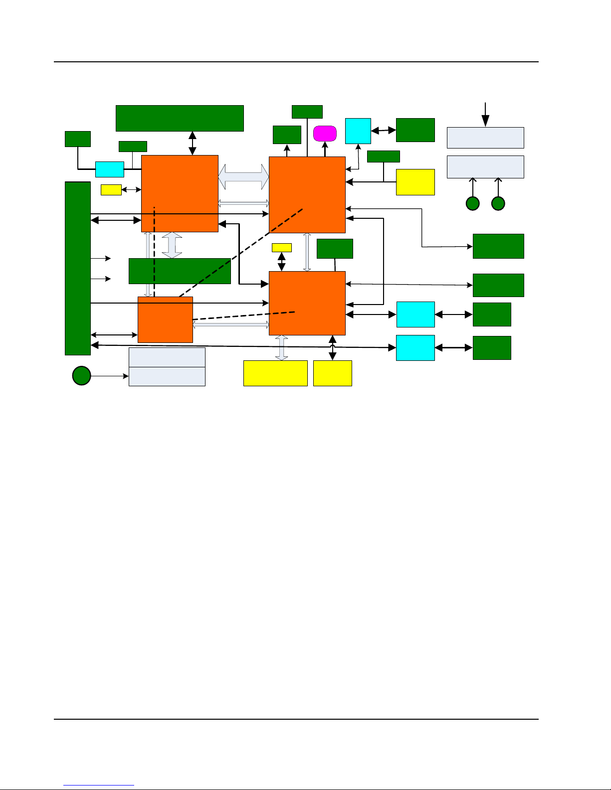
1.2.3 Board Architecture
Figure 2 displays the architecture of the Tsi620 evaluation board. The board includes the following
functional blocks; each block’s architectural features are discussed in the next section (see “Board
Hardware Functional Description”):
• sRIO switching and PrPMC module
• Stratix3 FPGA block
• TCI6488 DSP block
• GigE interface
• Clocking distribution
• Power management
• System controller
• AMC backplane and front panel connectors
Intergrated Device Technology
www.idt.com
Tsi620 Evaluation Board User Manual
60D7000_MA001_03
Page 12
12
AMC Finger Connector
Tsi620
SRIO Switch
SFP
Cage
SFP
Cage
TCI6488
DSP
Stratix3
FPGA
PrPMC Connector
AMC Ver tical Connector
DDR2 256MB
DSP
Emulator
x4 SRIO
x4 SRIO
PCI 32b/66M
‘XGMII
DDR2 32b/614M
x2 SRIO
OBSAI/CPRI
RJ45
x1 SGMI I
1000BaseT
OBSAI/CPRI (High Speed)
OBSAI /CPRI ( Low Sp eed)
POWER
Management
USB
SGMII
PHY
SPROM
SFLASH
4MB
CLOCK Management
RESET Contr ol
SPI
I2C
USB--
JTAG
Sync_SMA
PushButton
GPIO x 16
I2C
4x OBSAI/CPRI
Low Speed
AFS600
System
Controller
+12V@5A
Power Monitor
JTAG
RJ45
SGMII
PHY
x1 1000BASE- BX
LED
DIS
MMC
SYSCLK
JTAG
+12V
3.3V_MP
Mictor
AIF Port 1x OBSAI/CPRI
High Speed
MII
PHY
RJ45
100BaseT
Header
GPIO x6
GPIO x6
GPIO x4
Figure 2: Evaluation Board Architecture
1.3 Board Hardware Functional Description
1.3.1 sRIO Switching and PrPMC Module
Tsi620 sRIO switch provides the high-speed interconnection of AMC backplane, on-board vertical
AMC slot, Stratix3 FPGA, TI DSP, and the processor module (see Figure 3).
1.3.1.1 sRIO Switch
Tsi620 Evaluation Board User Manual
60D7000_MA001_03
• Tsi620 sRIO switch with an endpoint to PCI interface
• 4x sRIO link to AMC backplane with speed at 1.25 Gbaud. 2.5 Gbaud, and 3.125 Gbaud
• AMC finger connector with MMC support
• 4x sRIO link to on-board AMC slot connector with speed at 1.25 Gbaud, 2.5 Gbaud, and
3.125 Gbaud
• Conforms to AMC.1 and AMC.4 specification by PCIMG
• AMC.4 fabric port assignment support: Type4 (4x) only
• Two 1x sRIO links between TCI6488 and Tsi620
• XGMII interface to FPGA with 4x RapidIO protocol
Intergrated Device Technology
www.idt.com
Page 13

Figure 3: sRIO Switch and PrPMC Interface
SP0
SP2
4x SRIO
4x SRIO
SP4
SP5
1x SRIO
1x SRIO
SP6
4x FMAC
XGMI I R x 37pin
XGMI I Tx 37pin
SREP
PCI 32b 66M
AMC Finger
Connector
AMC Vertical
Connector
TCI6488
DSP
Stratix3
FPGA
Pr PMC 32 b
Connector
I2C
EEPROM
I2C_Master
PCI_CLK
PCI_Arbiter
TSI620 SRIO Switch
USB to
JTAG
JTAG
USB
S_CLK
156.25MHz
REF_CLK
CRSTn BRSTn
Reset
Controller
GPIO[0:15]
PCI_Reset
Pull-up/down
Resistors
PWRUP
CONFIG
GPIO[16:23]
1.2V3.3V 1.5V
INT(a,b,c,d)
MMC
156.25MHz
RX_CLK
JTAG
PHY
1x SGMII
RJ45
13
Table 1: sRIO Switch Power-Up Configuration Setting
Pin Name Setting Description
SP_HOST 0/1 0 = Not host
1 = Host (PrPMC is supposed to be the host) (S4 bit[1])
SP_MAST_EN 1 EndPoint can issue RapidIO Request packets
SP0_MODE_SEL 0 0 = 4x Connect to AMC vertical connector
SP2_MODE_SEL 0 0 = 4x Connect to AMC finger connector
SP4_MODE_SEL 1 1 = SP4 1x and SP5 1x connect to dual DSP 1x sRIO
SP6_MODE_SEL 1 1 = SP6 4x mode for FPGA I/F
SP_IO_SPEED[1:0] (10),01,00 10 = 3.125 Gb (Default)
SP_CLK_SEL[1:0] 01 01 = 156.25 MHz
SP(n)_PWRDN n=2,4,5,6 0 0 = Port 2, 4, 5, 6 are powered up (assuming SP(0) is always powered up)
Intergrated Device Technology
www.idt.com
01 = 2.5 Gb
00 = 1.25 Gb (S4 bit[4:3])
Tsi620 Evaluation Board User Manual
60D7000_MA001_03
Page 14
14
Table 1: sRIO Switch Power-Up Configuration Setting (Continued)
Pin Name Setting Description
SP(n)_PWRDN n=1,3 1 1 = Port 1 and 3 are powered down
SP_TX_SWAP 1 1 = Ports [0, 2, 4] Tx lane order is D, C, B, A
SP_RX_SWAP 1 1 = Ports [0, 2, 4] Rx lane order is D, C, B, A
1.3.1.2 Processor PMC (PrPMC) Interface
The PrPMC module is a high-performance, processor-based intelligent controller that can perform the
following functions:
• On-board system management
• Board software configuration
• Board booting control
• System interrupt handling
• Interface bridging between the module and the external networking system
• System operation status report and maintenance
• Baseband data processing assistance in real time
The PrPMC interface has the following features:
• Compliant to the following specifications:
— PCI Local Bus Specification (Revision 2.3)
— PCI Bus Power Management Specification (Revision 1.1)
— IEEE1386.1
— ANSI/VITA 32-2003
• PCI interface:
— 32-bit bus
— 33MHz/66MHz
— 3.3V signal only
— Tsi620 internal PCI arbiter
— Tsi620 PCI clock generator performs PCI clocking
— PCI interrupt handler: PrPMC module
— Tsi620 drives reset to PrPMC (PrPMC may issue system reset from PMC_RESETOUT#)
• PrPMC: system host for sRIO switching and monarch for PCI bus
• Physical position: PrPMC module located on AMC extension segment out of chassis
• Physical connector: 3x 64-pin CMC connectors (Jn1, Jn2, Jn3)
• Maximum power consumption: 24W
Tsi620 Evaluation Board User Manual
60D7000_MA001_03
Intergrated Device Technology
www.idt.com
Page 15

Table 2: PCI Interface Power-Up Configuration Setting
Pin Name Setting Description
PCI_RSTDIR 1 1 = PCI_RSTn is an output
PCI_M66EN 1/0 1 = 66MHz (PrPMC card could force it to 0 to 33 MHz operation using
S3 bit [1])
PCI_PLL_BYPASS 0 0 = PCI PLL is enabled
PCI_ARBEN 1 1 = PCI internal arbiter is used
PCI_HOLD_BOOT 0 0 = Release PCI software reset immediately after a Tsi620 reset is
completed
SPARE[1:0] 00 00 = Tsi620 (pull-up/down required for BOM selection)
Table 3: PrPMC Interrupt Routing
Interrupt Line Source Description
15
INTA Tsi620 Tsi620 interrupt output to PrPMC
INTB FPGA FPGA real-time events
INTC System Controller System administration coordination
INTD DSP DSP real-time events
1.3.1.3 XGMII FPGA Interface
• Tx/Rx clocking: synchronous 156.25, 125, or 62.5 MHz
• Tx_CLK: source to FPGA for RIO-XGMII interface clocking
• Signaling: HSTL-1.5V DDR
• Transmit: Tx_CLK, Tx_D[31:0], Tx_CTL[3:0], Tx_PHY_DISABLE
• Receive: Rx_CLK, Rx_D[31:0], Rx_CTL[3:0], Rx_ERROR
• The FPGA provides both on-chip parallel and serial termination for the XGMII interface.
Note: This feature is not supported on revision 1 of the prototype board.
1.3.1.4 JTAG, GPIO, and I2C
• Tsi620 supports I2C master mode or optional slave mode with jumper setting
• External socket I2C device with 8 DIP package (AT24C64B)
• Supports I2C configuration loading
• Uses FT2233D, USB to UART/FIFO controller, as USB to JTAG port converter
• Supports Tsi620 register access through JTAG port (mini-USB connector)
Intergrated Device Technology
www.idt.com
Tsi620 Evaluation Board User Manual
60D7000_MA001_03
Page 16
16
• Mini USB connector on front panel with USB2.0 compatible
• Tsi620 GPIO[0:15] connection to DSP and FPGA
• Standard JTAG header for Tsi620 on-die scope support
Table 4: I2C Power-Up Configuration Setting
Pin Name Setting Description
I2C_MA (PU) 0 1 = Multi-byte peripheral addressing
I2C_SA[6:0] (PU) 0000000 I2C port slave address
I2C_SLAVE (PU) 0 0 = Disable the I2C slave mode
I2C_SEL (PU) 0 only 0 = Asserted, I2C_SA[1,0] are used as the lower 2 bits of EEPROM
I2C_DISABLE (PD) 0/1 0 = Enable I2C register loading
1 = Disable I2C register loading (DIP Switch, S4 bit [2])
Table 5: Tsi620 GPIO Signal Assignment
GPIO Signal Connect To Description
GPIO[0:15] FPGA Intercommunicating between Tsi620 and FPGA
GPIO[16:23] DIP Switch and LED GPIO[16:19] connected to DIP Switch S2[1:4]
GPIO[20:23] connected to LED D3, D5, D6, and D4, respectively
GPIO[24:31] LED, Test point Intercommunicating between Tsi620 and the system controller (AFS600)
1.3.1.5 AMC Interfaces
• AMC finger connector supports sRIO AMC backplane
• AMC finger connector supports MMC including I2C
• AMC finger connector supports port 0 GigE (1000Base-BX) interface to RJ45 through the
VSC8221 PHY (AMC.2)
• AMC finger connector does not support JTAG
• 3.3V management power; maximum 100 mA from figure connector
• AMC vertical slot connector does not support JTAG, I2C, and MMC functions
• AMC vertical slot shared with 12V power and local 3.3V
• Total power consumption including PrPMC and AMC slot should not be more than 60W
Tsi620 Evaluation Board User Manual
60D7000_MA001_03
Intergrated Device Technology
www.idt.com
Page 17
1.3.2 FPGA Block
30.72MHz_REF
Stratix3 FPGA
780FBGA
EP C S64 AS-CF GHeader
RIO
XGMI I
OBSAI
Frame_Sync
XGMI I R x 38pi n
XGMI I Tx 38pin
Tsi620
GPIO[0:15]
156. 25M
DDR
PLL
x1
RX_CLK
PLL
x10
PLL
x8/10
GigE_ REF(p,n)
SFP
SMT_IN
FSYNC_OUT
FSYNC_IN
156. 25MHz
Mictor
Switching
Fabric
LED
Display
OBSAI
SERDES
O
B
S
A
I
7
6
8
M
b
/
C
P
R
I
6
1
4
.
4
M
b
DSP
JTAG
EMAC
10/100M
PHY
MII
RJ45
100B aseT
The Altera Stratix3 FPGA can function as either a baseband data processing engine or as an accelerator
to assist DSP baseband data processing (see Figure 4). The FPGA block includes a 780-pin FPGA,
FPGA configuration, RIO XGMII interface, and an antenna interface.
1.3.2.1 FPGA Device
• Altera Stratix3 EP3SL150 in 780-pin BGA
• Package: 29 x 29 mm, 780-pin FBGA with 1 mm pitch
• Speed grade: -3
• Core voltage: 1.1V
• Clock tree performance: 450 MHz for -4 grade
• Maximum IO pins: 480
• Maximum allowed power consumption: 10W
Figure 4: FPGA Block Diagram
17
Intergrated Device Technology
www.idt.com
Tsi620 Evaluation Board User Manual
60D7000_MA001_03
Page 18

18
1.3.2.2 RIO XGMII Interface
• Up to 12-Gb bandwidth of data transfer between FPGA and sRIO switch
• Reference clock: RX_CLK from Tsi620
• Frequency: 62.5, 125, or 156.25 MHz (Note: Revision 1 of the Tsi620 evaluation board does not
support 156.25 MHz.
• Tx_CLK: sync with Rx-CLK and must be PLL locked before driving out
• Signaling: HSTL-1.5V Class-II
• Termination: FPGA on-die parallel 50-ohm termination for the receiver and on-die 25 ohm serial
termination for the transmitter
• Protocol: RapidIO for logical and transport layers
• Rx: 38 signals
• Tx: 38 signals
1.3.2.3 RF Antenna Interface
• Compliant specifications: CPRI specification v2.1, OBSAI v2.0, OBSAI RP3 v4.0
• Supports 1x link to SFP connector with OBSAI-768 Mb or CPRI-614.4 Mb
• Supports 4x link to DSP with OBSAI-768 Mb or CPRI-614.4 Mb
• Clocking Source: FPGA local PLL with reference clock at 30.72 MHz and LVDS/LVPECL logic
1.3.2.4 OBSAI System Clock an Synchronization
• Compliant specifications: OBSAI RP1 standard
• Source mode: AMC backplane or SMA connectors
• System clock input: 30.72 MHz with LVDS/LVPECL logic standard
• Frame synchronization burst input: 3.84 MHz with LVTTL logic
• FPGA outputs the system synchronization signals to the DSP Frame Sync Module (FSM)
1.3.2.5 EMAC 100BaseT Port
• 10Mb/100Mb BaseT with MII interface
• External PHY to RJ45 connector
1.3.2.6 FPGA Testing Support
• 2-digit LED display
• One Mictor connector
• One 2-bit DIP switch
Tsi620 Evaluation Board User Manual
60D7000_MA001_03
Intergrated Device Technology
www.idt.com
Page 19

1.3.2.7 FPGA Configuration
• Configuration mode: Active serial and JTAG
• Serial configuration device: EPCS64, 3.3V, 67 Mb, 16-pin SOIC
• Dedicated header support USB blaster programming cable
• Dedicated JTAG port for FPGA JTAG configuration and debugging
• Voltage: 3.3V
1.3.3 DSP Block
The DSP block includes TI TCI6488 DSP, DDR2 memory, antenna interface, sRIO links, serial flash,
GigE link, and JTAG emulation port (see Figure 5). The TI TCI6488 is the major baseband processing
engine on the Tsi620 evaluation board.
1.3.3.1 TCI6488 DSP
• DSP core: Triple C64X+
• Core frequency: 983 MHz (61.44Mx16)
• Core PLL multiplier: 4 ~ 16
19
• Core reference clock: 61.44 MHz
• Cache: L1-64 KB, L2-3 MB
• Boot mode: I2C, EMAC, sRIO
• 16-bit GPIO assignment:
— 4 bits to FPGA
— 4 bits to Tsi620 through AFS600
— 1 bit to PrPMC for interrupt
— 1 bit to AFS600 for status report
— 6 bits for DSP local configuration
• Package: 561-pin, 23 x 23 mm BGA with 0.8 mm pitch
• Voltage supply: core-1.1V SerDes-1.1V, IO-1.8V
• Power consumption: max 8W
• Thermal dissipation management: Passive heat-sink, core voltage auto-scaling
Intergrated Device Technology
www.idt.com
Tsi620 Evaluation Board User Manual
60D7000_MA001_03
Page 20

20
DDR2
SDRAM
64Mx16b
DQ[0:31]
DQS( p,n)
ADD/
CTRL
DDR2 Controller
CK/ CK#
DDR
PLL
DDRREFCLK(p,n)
61.4 4MHz
307.2MHz
SRIO
SERDES
PLL
RIOS GMIIR EFCLK(p,n)
LVPECL/
156.25 MHz
1x SRIO
1x SRIO
Tsi620
SRIO
SWITCH
EMAC
SGMII
GIGE SGM II
SGMII
PHY
AIF
PLL
STSCLK(p,n)
61.44M Hz
OBS AI /CPRI I/F
FSYNC
FBURST(p,n)
O
B
S
A
I
7
6
8
M
b
/
C
P
R
I
6
1
4
.
4
M
b
SFP
BcB SP
SPI-Master
Serial
FLASH
8MB
FPGA
SPI Bus
3.3V-1.8V
LevelShifter
1.8V
PORZz
XWRSTz
MDI
I2C
EEPROM
60pin Port
Emulation
JTAG
TCI6488 DSP
RJ45
w/ Mag
GIGE SGM II
1x Link
4x Link
1x Link
AMC
GPIO x 16
FPGA
AFS600
x4
x6
x6
Conf igurati on
Figure 5: DSP Block Diagram
1.3.3.2 DDR2 SDRAM Memory
• DDR2 memory device: 2x MT47H64MHR-3, 64Mx16b-677M
• Interface speed: 307.2 MHz or 614.4M DDR
• Memory size: 256 MB
• DDR PLL provide the clocking to DDR2 SDRAM
• Interface data width: 32 bit
• Reference clock: 61.44 MHz
• I/O Standard: SSTL-1.8V
1.3.3.3 Antenna Interface
Tsi620 Evaluation Board User Manual
60D7000_MA001_03
• Antenna I/F link: 1x to SFP connector with up to 3 Gbps
• Antenna I/F link: 1x to AMC backplane Port 17 with up to 3 Gbps
• FPGA link: 4x to FPGA with up to 768 Mbps per lane
• CPRI compatible: 614.4 Mbps, 1.2288 Gbps, 2.4576 Gbps link rates
• OBSAI compatible: 768 Mbps, 1.536 Gbps, 3.072 Gbps link rates
Intergrated Device Technology
www.idt.com
Page 21

• Reference clock: 61.4 MHz LVDS/LVPECL
• Frame synchronization: receive the system clock and synchronization burst from FPGA
1.3.3.4 sRIO Links and GigE Port
• Two x1 sRIO links to Tsi620
• sRIO link rates: 1.25 Gbps, 2.5 Gbps, and 3.125 Gbps
• One GigE link with SGMII interface
• Reference clock: LVPECL 156.25 MHz
• MII interface to GigE switch and GigE PHY through 3.3V to 1.8V level shifter
• One RJ45 connector with integrated magnetic
• 10/100/1000BaseT capable
• VSC8221 GigE-PHY SGMII interface
• MII port controller by DSP
1.3.3.5 Serial FLASH
21
• McBSP0 is configured to SPI bus master to support serial flash memory
• Serial flash can store the boot loader or software image
• Serial flash: SF25L064, 64 Mb, 50 MHz SPI, 3.3V device
• 3.3V to 1.8V level shifter is required between DSP and Serial flash
1.3.3.6 EEPROM and Emulation Interface
• 1.8V I2C EEPROM, AT24C64B-10TU-18
• Support emulation interface with 60-pin emulation connector
1.3.3.7 DSP Interrupt Assignment
• Three non-mask interrupts with active high are routed to FPGA for user-defined usage.
• Interrupts between DSP and FPGA through DSP_GPIO[12:15] with active low
• Interrupts between DSP and Tsi620 by DSP_GPIO[6] through the AFS600 as the level shift.
Note: Care must be taken that the interrupt signals must be always driven after the reset once their
direction and function has been defined.
• The DSP is responsible for managing two GiGe PHYs and two GiGe PHY MI interface interrupts
(MINT# is connected to DSP_GPIO[7] pin).
Intergrated Device Technology
www.idt.com
Tsi620 Evaluation Board User Manual
60D7000_MA001_03
Page 22
22
3.3V_MP
1.5V
AFS600
Flash-FPGA
Analog
Bank
REFCLK
IPMB
Power Monitoring
Reset
Control
25MHz
SYN C_CLK
3.3V_Prog
1.5V_Reg
JTAG
R/C
2.5V
Bank
3.3V
Bank
1. 8 V
Bank
Pushbutton
DSP
SMT_CLK
MMC
GPIO
GPIO
FRAME-
SYNC
Tsi620
3.3V
Bank
LVDS
LVDS
UART
3.3V
Bank
USB
I/F
McBSP
1.3.4 System Management Controller
The system management controller is implemented with an Actel FPGA AFS600-256, which is a flash
memory based mixed signal FPGA (see Figure 6). This FPGA has an embedded processor and is
mainly powered by 3.3V_MP from an AMC finger connector since the system controller must be
functioning whenever 3.3V_MP is available.
1.3.4.1 System Controller Functionality
• Board reset control
• Board power sequencing control and power monitoring
• Real-time clock
• AMC MMC (Memory management control)
• Multi-voltage level conversion
• UART port to USB interface
• Board status report
For more information on the function of the system controller, see the source files for the
Tsi620 Evaluation Board System Controller (35D7000_PL007).
Figure 6: System Management Controller
Tsi620 Evaluation Board User Manual
60D7000_MA001_03
Intergrated Device Technology
www.idt.com
Page 23

1.3.4.2 AFS600-FBGA256 Implementation
• Bank 0: 1.8V LVCOMS1V8
• Bank 1: 3.3V LVTTL, LVCOMS, LVPECL
• Bank 2: 2.5V LVCOMS2V5
• Bank 4: 3.3V LVTTL, LVCOMS, LVPECL
• Analog Bank: 0 ~ 12V power monitoring
• Power: 3.3V_MP only with max. 100mA
1.3.4.3 Reset Control
The Actel Flash FPGA is used on the evaluation board to implement the module management
controller of the AMC interface. The Actel FPGA also functions as the central reset controller to
handle the reset control glue logic.
Reset Control Requirement
Table 6: Major Components Reset Signal List
23
Devices Reset Signal Logic Function
Tsi620 CHIP_RSTn 3.3VLVTTL Tsi620 chip reset
Tsi620 BLOCK_RSTn 3.3VLVTTL Tsi620 block reset
TI-DSP PORz 1.8VLVCOMS DSP power-on reset. Held low >1 ms after power and clk
TI-DSP XWRSTz 1.8VLVCOMS DSP warm reset. No affect on PLL and emulation
FPGA HRSTn 3.3VLVTTL FPGA power-on reset and trigger device reset
FPGA SRSTn 3.3VLVTTL FPGA soft reset and no affect to PLL
V8221 HRESETn 3.3VLVTTL GigE PHY reset
Reset Control Logic
• System management controller: Actel AFS256-FG256, Flash-based mixed signal FPGA
• Supports multi-volt device control
Intergrated Device Technology
www.idt.com
Tsi620 Evaluation Board User Manual
60D7000_MA001_03
Page 24

24
PrPMC
DSP
Tsi620
AFS600
System
Controller
Chip_RSTn
PORn
Push
Button
Power
Monitor
XWRSTn
FPGA
HW_RSTn
SW_RSTn
GigE
PHY
RSTn
PCI_RSTn
Block_RSTn
Interrupts
RSTOUTn
CLK_RSTn
Status
Figure 7: Reset Control Illustration
1.3.4.4 MMC Implementation
The MMC’s design is based on Actel’s MMC reference design, which has been customized with an
extended analog block for additional on-board voltage, current, and temperature monitoring functions.
The Actel MMC reference design is a custom 8051-based microcontroller implemented in an Actel
AFS600-FG256 Fusion mixed-signal FPGA, and is supported by IPMI firmware from uBlade. The
MMC design supports the basic requirements defined by the PICMIG AMC.0 and Intel IPMI v2.0
specifications. For additional information about the MMC design, contact the Actel or IDT Technical
Support team.
1.3.5 Clocking Management
This section specifies the clocking generation and distribution implementation.
1.3.5.1 Clocking Source Requirement
General requirements for all clocking sources:
• Stability: +/-100 ppm
• Duty cycle: 40/60%
• Trise/Tfall: 50 ps–1300 ps for 20% to 80% swing
Tsi620 Evaluation Board User Manual
60D7000_MA001_03
Intergrated Device Technology
www.idt.com
Page 25

Table 7 summarizes the clocking sources requirements for all major components on the Tsi620
evaluation board.
Table 7: Clocking Sources List
Clock Name Function/Domain Logic Standard Frequency Input Jitter
25
SCLK(p,n) Tsi620 system
reference
SP6_RXCLK Tsi620 XGMAI RXCLK HSTL-1.5V 62.5 MHz, 125 MHz,
PCI_CLK Tsi620 PCICLK input PCI-3.3V 66.7 MHz/33.3 MHz +/-100 ps
RIO_XGMII_RxCLK FPGA XGMII RxCLK
input from Tsi620
GigE_REFCLK FPGA GigE EMAC
reference
AIF_REFCLK FPGA OBSAI/OPRI
reference
SYSCLK{p,n} DSP core and AIF
reference
DDRREFCLK(p,n) DSP DDR2 reference LVDS/PECL(AC) 61.44 MHz 75 ps (pk2pk)
RIOSGMIICLK(p,n) DSP sRIO and SGMII
reference
LVDS/PECL(AC) 156.25 MHz
175 ps (pk2pk)
156.25 MHz
HSTL-1.5V 62.5 MHz, 125 MHz,
156.25 MHz
LVDS/PECL(AC) 156.25 MHz
LVDS/PECL(AC) 30.72 MHz
LVDS/PECL(AC) 61.44 MHz 2 ps RMS
LVDS/PECL(AC) 156.25 MHz 4 ps RMS
56 ps (pk2pk)
GigE PHY_REFCLK GigE PHY Crystal 25 MHz
AFS600_REFCLK AFS600 reference
clock
Internal RC 100 MHz +/-1%
1.3.5.2 Clocking Architecture Implementation
There are two clock synthesizers on board that provide the reference clocking required for the FPGA,
DSP, and sRIO switch. The first synthesizer has a 25-MHz crystal source: it outputs 156.25 MHz with
LVPECL logic to serve sRIO system reference clock, FPGA EMAC and SGMII reference, and DSP
sRIO and SGMII reference. The second clock synthesizer has a 30.72-MHz oscillator source: it
supplies 30.72 MHz and 61.44 MHz CML clocking references for the DSP, DDR2, FPGA antenna
interface, DSP core PLL, and DSP antenna interface (see Figure 8).
In order to simplify the clocking architecture, both the DSP core frequency and the on-board DDR2
memory operation frequency, run at slightly lower than their maximum specification. Both DSP and
DDR2 memory use the same clocking source at 61.44 MHz, DSP core frequency is 983 MHz, and
DDR2 memory operates at 614.4 M double data rate.
Intergrated Device Technology
www.idt.com
Tsi620 Evaluation Board User Manual
60D7000_MA001_03
Page 26

26
Tsi620
25MHz
Crystal
ICS843004
CLK Synthesizer
LVPECL/156.25M
SCLK TxCLK
PCLKOUT PCLKIN
PCI3V3/
66.7M
FPGA
RxCLK
PrPMC
HSTL-1.5
62.5/125/
156.25M
HSTL-1.5
XGMII
PLL x1
Sync to RxCLKin
LVPECL/156.25M
AIF
PLL
sRIO
PLL
SGMII
PLL
LVPECL/
156.25M
AFS600
CDCL6010
CLK Synthesizer
OBSA
PLL
CML/61.44MHz
DDR2
PLL x10
DDR2
SSTL-1.8
307.2M
30.72MHz
LVDS
Core
PLL
DSP
I2C
614.4Mb/
768Mb
OBSAI/CPRI
4to1
MUX
30.72MHz
OSC
FPGA
AFS600
CML/61.44MHz
CML/61.44MHz
CML/61.44MHz
CML/30.72MHz
30.72MHz
SERDES
PLL
SMT
AMC
25MHz
OSC
GigE
PHY
GigE
PHY
MII
PHY
LVPECL/156.25M
The Tsi620 FMAC and FPGA RIO-XGMII interface function in the synchronous mode. The TX_CLK
from the Tsi620 is sourcing from its SYSCLK(p,n), while the FPGA must use RX_CLK as its
RIO-XGMII operation reference clock. The TX_CLK driven from the FPGA must therefore be
synchronized with TX_CLK driven by the Tsi620. In addition, TX_CLK of the FPGA cannot be
applied to the Tsi620 until the FPGA PLL is locked.
Figure 8: Clocking Generation and Distribution
The FPGA XGMII PLL is synchronized to received RX_CLK from the Tsi620.
CDC6010 must be managed through its serial interface, while the DSP is responsible for CDC6010
configuration through its I2C bus.
1.3.6 Power Management
1.3.6.1 Power Supply and Consumption Analysis
The board power distribution design must comply with AMC.1 power management requirements. The
Tsi620 Evaluation Board User Manual
60D7000_MA001_03
AMC card has only single +12V supply available from either AMC finger connector or DC barrel plug:
• AMC max power consumption: <60W including all add-in cards
• AMC finger connector: 12V@5A for MicroTCA chassis operation
• DC barrel plug: 12V@5A for stand-alone operation
The clock synthesizer
Intergrated Device Technology
www.idt.com
Page 27

Table 8 summarizes the major components’ supply requirements and max potential current demand.
Table 8: Major Components Power Supply Requirement (Power Budget)
27
Device 1.1V 1.2V 1.5V 1.8V 2.5V 3.3V 3.3VSB 5V 12V Notes
Tsi620 3A 0.5A 0.5A <4.7W, sequencing
TCI6488 7A+1A 1A <9W, sequencing req.
EP3SL150 8A 0.5A 0.5A 0.5A 0.5A Assume <10W (TBV)
DDR2 x6 0.7A 350mA x2
VCS8221x2 0.5Ax2 <0.8w inner reg@1.2v
S25FL064 IG
PrPMC 4.5A 3A 0.5A Tall<25W, -12V@0.5A
AT24C512 IG
AMC SLOT 3A ½(60W)=30W
AFS600 80mA 0.1A 3.3V_MP@100mA
CDCL6010 0.5A
AMC FGR -6A 8V~14Vin, 60W
Ex Power -5A From DC barrel plug
a
LED 0.5A
Total 8A+8A 3A 1A 3A 0.5A 7A 1A 3A
a. IG = Ignore, FGR = Finger connector.
1.3.6.2 Power Distribution Implementation
• The LTM4601, LTC DC/DC switching micro module generates +5V, +3.3V, 1.1V_DSP, and
1.1V_FPGA (see Figure 9)
• 4x LTM4601 work in synchronous mode and are controlled by a 4 phase PLL driver
• TCI6488 power management supports the core voltage scaling for power consumption
auto-control
• TCI6488 SerDes 1.1V supply comes from FPGA_CORE_1.1v
• Both LTM4601and TI switching modules support auto-tracking, which is used for silicon power
sequencing control
• The LTM4604, 4A, (15 mm x 9 mm x 2.3 mm) DC/DC switching regulator generates +1.2V,
+1.5V, +1.8V, and +2.5v from either 5V rail or 3.3V rail.
• -12V is implemented on-board for PrPMC only with max I <= 350mA
Intergrated Device Technology
www.idt.com
Tsi620 Evaluation Board User Manual
60D7000_MA001_03
Page 28

28
1.3.6.3 Power Monitoring and Sequencing Control
• The Actel AFS600 is the on-board power monitor and power-on sequencing controller, and should
be working whenever 12V and 3.3V_MP are available. A 2.5V reference and a couple of
comparators are used to assist the sequencing control.
• Tsi620 sequencing: 1.5V1.2V3.3V
• TI-DSP sequencing: 1.8V 500uS CVdd and 1.1V
• FPGA sequencing: VCCio VCCcore
• Proposed sequencing: 12V 5V 1.5V 1.2V 3.3V 2.5V 1.8V 1.1V_core +
1.1V_dsp
• 3.3V_MP (100mA) is for AFS600. 3.3VSB is only working in stand-alone mode
The power-up sequencing has four stages:
1. After 3.3V_MP available, the AFS600 system controller is functioning and waiting for +12V from
the AMC backplane once the Hot Swap handler is closed.
2. When +12V is powered up and SW2 is turned on, the AFS600 signals to start +5V, 1.5V, and 1.2V.
3. After 1.2V is powered up, the third power chain, +3.3V, 2.5V, and 1.8V, start to ramp up.
4. When 1.8V power-good is detected, the sequencing control logic turns on the 1.1V_DSP and
1.1V_FPGA rails.
1.3.6.4 Power Consumption Assumption
The real power consumption of PrPMC and FPGA are critical to the power management. An active
cooling fan is required for the FPGA, and passive cooling heat sinks are needed for the DSP and
Tsi620.
• Assuming the power consumption of PrPMC module is <15W
• Assuming the power consumption of FPGA is <5W
• Assuming the power consumption of DSP + DDR2 are <10W
• Assuming the power consumption of MISC is <10W
• Assuming the power consumption of Tsi620 is <5W
So, the maximum power consumption allowed for the AMC vertical slot is <15W.
Tsi620 Evaluation Board User Manual
60D7000_MA001_03
Intergrated Device Technology
www.idt.com
Page 29

Figure 9: Power Distribution and Management
AMC12Vin
Plug-DC12Vin
@5A
@5A
DC/DC SW
LTM 4601
5V@ 8A
DC/DC SW
LTM 4601
3.3V@12A
DC/DC SW
LTM 4601
1.1V_DSP@10A
DC/DC SW
LTM 4601
1.1V@ 10A
DC/DC SW
LTM 4604
DC/DC SW
LTM 4604
DC/DC SW
LTM 4604
1.8V@4A
1.2V@ 4A
1.5V@ 2A
DC/DC SW
LTM 4604
2.5V@ 1A
5V@3A
3.3V@7A
DSP_IO,
AMC-Slot, PrPMC
FPGA
Tsi620_CORE
PrPMC, TSI620_IO
MISC_Devices
FPGA_IO, Tsi620_IO
DDR2 Memory
DSP_SERDES
FPGA_CORE
Scale
3.3VSB@1.0A
System
Management
+5V@3.5A
AFS600
Reset
Filters
1.1V@1.0A
DSP_CORE
Regulat or
senser
PLL Sy nc
PrPMC
FPGA_IO
-12V@0. 5A
Regulat or
PrPMC
Power
Monitoring
Sequencing
Control
Sequencing
29
1.3.7 JTAG Port and I2C Bus
1.3.7.1 JTAG Interface Implementation
• The Altera FPGA and Actel FPGA are in the same 3.3V JTAG chain (they share the single 10-pin
JTAG header)
• Tsi620’s internal registers can be accessed by either USB or JTAG header
Intergrated Device Technology
www.idt.com
Tsi620 Evaluation Board User Manual
60D7000_MA001_03
Page 30

30
System I2C Bus 3.3V
Tsi620
I2C
SFP2
EEPROM
SFP1
EEPROM
DSP
I2C
1.8V I2C Bus
CDCL
6010
• The FDTI-2232D is self-powered by 3.3V_USB from the mini-USB connector. It provides bridges
the USB interface and JTAG port for the Tsi620, and also provides a USB to UART interface for
the AFS600.
• JTAG connectors for the following:
— TI 6488 DSP (60-pin emulator)
— Tsi620 JTAG
— Actel FPGA and Stratix3 JTAG chain access
1.3.7.2 Local I2C Bus
There are two segments of the local I2C bus (see Figure 10):
• 3.3V I2C bus: The Tsi620 is I2C master. This bus includes the Tsi620 I2C EEPROM and two SFP
optical transceivers.
• 1.8V I2C bus: The DSP is I2C master. This bus includes the DSP, I2C EEPROM, and CDCL6010.
Figure 10: Local I2C Bus Connection
1.4 PCB Characteristics
1.4.1 PCB Form Factor
• Board form factor: AMC single width module
• Module dimension: 73.5 mm x 350 mm (Out-chassis section length 169 mm)
• Module height: Full height, components side 1 is <13.7 mm; components side 2 is <2.5 mm
• Thickness: 1.6 mm+/-10 %
• No mechanical front panel (face-plate) implemented
• Additional stand off or mounting holes are available for both chassis and standalone operation
Tsi620 Evaluation Board User Manual
60D7000_MA001_03
Intergrated Device Technology
www.idt.com
Page 31

1.5 Configuration Options
ON: represent “0” or logic “Low”
OFF: represent “1” or logic “High”
This section describes the configuration options for the Tsi620 evaluation board.
1.5.1 DIP Switches
Switches S1 to S5 combine four small slide switches identified with numbers 1 to 4 (see example in
Figure 5). For information on the individual DIP switches, see Tables 9 to 13.
31
Intergrated Device Technology
www.idt.com
Tsi620 Evaluation Board User Manual
60D7000_MA001_03
Page 32

32
1.5.1.1 S1 – DSP Boot-mode Setting
Table 9: S1[1:2:3:4] BSP Boot-mode Setting
Switch S1[1:2:3:4] BOOTMODE[0:3] DSP Boot-mode Note
ON-ON-ON-ON 0-0-0-0 No Boot
OFF-ON-ON-ON 1-0-0-0 I2C Master Boot A Not supported
ON-OFF-ON-ON 0-1-0-0 I2C Master Boot B I2C address at 0x51
OFF-OFF-ON-ON 1-1-0-0 I2C Slave Boot
ON-ON-OFF-ON 0-0-1-0 EMAC Master Boot
OFF-ON-OFF-ON 1-0-1-0 EMAC Slave Boot
ON-OFF-OFF-ON 0-1-1-0 EMAC Forced-Mode Boot
ON-OFF-ON-OFF 0-1-0-1 sRIO Boot – 1.25 G CFG2 - 1.25 G (Default)
OFF-OFF-ON-OFF 1-1-0-1 sRIO Boot – 3.125 G CFG3 – 3.125 G
All others Reserved
1.5.1.2 S2 – Tsi620 GPIO Setting
Table 10: S2[1:2:3:4] Setting
Switch S2 Signal Assignment Default ON/OFF Setting
Bit 1 Tsi620_GPIO16 OFF ON = 0 or logic low
OFF = 1 or logic high
Bit 2 Tsi620_GPIO17 OFF ON = 0 or logic low
OFF: 1 or logic high
Bit 3 Tsi620_GPIO18 OFF ON = 0 or logic low
OFF = 1 or logic high
Bit 4 Tsi620_GPIO19 OFF ON = 0 or logic low
OFF = 1 or logic high
Tsi620 Evaluation Board User Manual
60D7000_MA001_03
Intergrated Device Technology
www.idt.com
Page 33
1.5.1.3 S3 – MISC Setting
Table 11: S3[1:2:3:4] Setting
Switch S3 Signal Assignment Default ON/OFF Setting
Bit 1 PCI_M66EN 1 = OFF ON = Force PCI bus clock at 33 MHz
OFF = Set PCI bus clock at 66 MHz
Bit 2 Tsi620_BCE 1 = OFF ON = Set Tsi620_BCE to “0” for on-die-scope operation
OFF = Normal operation
Bit 3 FPGA_SET_3V3 1 = OFF ON = 0 or logic low to FPGA
OFF = 1 or logic High to FPGA
Bit 4 AFS_SET_3V3 1 = OFF Reserved
1.5.1.4 S4 – Tsi620 Option Setting
Table 12: S4[1:2:3:4] Setting
33
Switch S4 Signal Assignment Default ON/OFF Setting
Bit 1 TSI620_SP_HOST 1 = OFF ON = Force PCI bus clock at 33 MHz
OFF = Set PCI bus clock at 66 MHz
Bit 2 TSI620_I2C_DISABLE 1 = OFF ON = Set Tsi620_BCE to 0 for on-die-scope operation
OFF = Normal operation
Bit4_Bit3 TSI620_SP_IO_
SPEED[1:0]
1_0
OFF_ON
0_0 = 1.25 Gbps sRIO link
0_1 = 2.5 Gbps sRIO link
1_0 = 3.125 Gbps sRIO link
1_1 = Reserved
1.5.1.5 S5 – DSP Clocking Setting
Table 13: S5[1:2:3:4] Setting
Switch S5 Signal Assignment Default ON/OFF Setting
Bit 1 CORECLKSEL 1 = OFF ON = Force PCI bus clock at 33 MHz
OFF = Set PCI bus clock at 66 MHz
Bit 2 FPGA_SET_1V8 1 = OFF ON = 0 or logic low to FPGA
OFF = 1 or logic high to FPGA
Bit4_Bit3 30M72_SEL[0:1] 0_0
Intergrated Device Technology
www.idt.com
ON_ON
0_0: On-board 30.72 MHz oscillator
0_1: 30.72 MHz from AFS600
1_0: 30.72 MHz from FPGA
1_1: External 30.72 MHz clock from SMA J13
Tsi620 Evaluation Board User Manual
60D7000_MA001_03
Page 34

34
1.5.2 Jumpers
The Tsi620 evaluation board has only one jumper, J6, which is reserved for the future use. This jumper
should be left open for the normal operation.
1.5.3 Push Button and Toggle Switch
Reference Designator Switch Type Signal Assignment Function Description
SW1 Push button SOFT_RESETN When the button is pushed, the following
occurs:
• Negative asserted at Tsi620 pin, BLK_RSTN
• Negative asserted at DSP pin, XWRSTN;
and FPGA pin, FPGA_SRSTN
• Negative asserted at GigE PHY VSC8621
pin, SRESETN
SW2 Toggle Switch POWER_ON/OFF
HotSwap_
OPEN/CLOSE
SW3 Push button SYSTEM_RESETN When the button is pushed, the following
In non AMC-Chassis mode, after +12V applied,
SW2 functions as the power sequencing
ON/OFF switch.
In AMC-Chassis mode, SW2 functions as Hot
Swap switch
When switch handler position points to RJ45
side, it represents as “Power OFF” or “Hot
Swap Switch Open”.
When switch handler position points to push
button side, it represents as “Power ON” or
“Hot Swap Switch Close”.
occurs:
• Negative asserted FPGA pin, NCONFIG, for
FPGA re-configuration
• Negative asserted FPGA pin, FPGA_HRSTN
• Negative asserted Tsi620 pin, CHIP_RSTN
and TRSTN
• Negative asserted USB_RSTN
• Negative asserted DSP pin, PORSTN
• Negative asserted GigE PHY pin, HRSTN
• Positive asserted U7, 156.25M PLL buffer,
pin MR
Tsi620 Evaluation Board User Manual
60D7000_MA001_03
Intergrated Device Technology
www.idt.com
Page 35

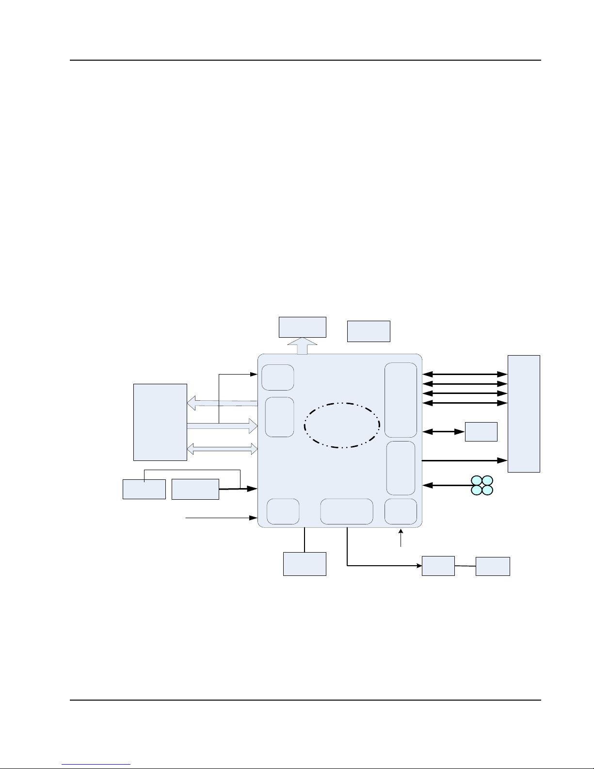
Figure 11: Location of Switches and Connections
Tsi620 EVB Placement Top View
S1
S2
S3
S4
J14-FPGA SFP
J15-DSP SFP
U35
Mini-USB
U26
FPGA-RJ45
U34
GigE-RJ45
SW2
ON/OFF
J4: Mictor
U29
+12Vin
J2: DSP
Emulator Port
J10
Tsi620 JTAG
P1: AMC Slot
J5
FPGA Active
Serial
Programming
U21
U22
2-Chars
LED Display
SW1:
Soft-Reset
SW3:
System-Reset
J13: SMA
ExCLK 32.72MHz
DSP-GigE
AMC-GigE
J7/J8 & J11/J12
SMA to FPGA
S5
JN2
JN1
JN3
Tsi620 EVB Placement Bottom View
PrPMC
Connector
J9
FPGA JTAG
35
Intergrated Device Technology
www.idt.com
Tsi620 Evaluation Board User Manual
60D7000_MA001_03
Page 36

36
1.6 Board Connectors
This section discusses the external connectors on the Tsi620 evaluation board.
The pin definition for each board connector is not included in this document. For information
on pin assignments, see the Tsi620 evaluation board schematics (60D7000_SC003).
1.6.1 JTAG and FPGA Programming Connectors
Reference
Connector Name
DSP Emulator J2 A dedicated 60-pin header for TI DSP emulator connection
FPGA Programmer J5 A dedicated 10-pin header for Altera FPGA active serial flash programming
Designator
Function Description
FPGA JTAG J9 A 10-pin header of the JTAG chain of both Actel FPGA and Altera FPGA. The header
supports both Actel and Altera FPGA programming download cables.
Tsi620 JTAG J10 A dedicated 16-pin header for the Tsi620 JTAG port; this header is pin-matched to a
Wiggler JTAG cable.
USB Port U35 A mini-USB port to access the Tsi620 JTAG port or AFS600 UART port through an
FTDI FT2232D converter.
a. The header supports both Actel FPGA and Altera FPGA JTAG access only when both FPGAs are powered up. IDT does not
recommend re-programming the Actel FPGA without consulting the IDT Technical Support team.
b. Both J10 and U35 can be used to access the Tsi620’s internal registers through its JTAG port; however, they work exclusively.
c. FT2232D has independent USB-to-JTAG and USB-to-UART channels.
b
c
a
1.6.2 Communication Interface Connectors
Reference
Connector Name
FPGA RJ45 U26 A dedicated RJ45 port for Altera FPGA 10/100BaseT Ethernet interface
GigE RJ45 U34 Dual RJ45 Jack for GigE interface
Designator
Function Description
Upper RJ45 port: AMC-SGMII GigE port
Lower RJ45 port: DSP-SGMII GigE port
FPGA SFP J14 A dedicated FPGA SFP connector of antenna RF SerDes interface for OBSAI at
DSP SFP J15 A dedicated DSP SFP connector of antenna RF SerDes interface for OBSAI at
a. IDT recommends Avago optical transceiver: AFBR-57J5APZ, tri-speed OBSAI/CPRI optical transceiver.
Tsi620 Evaluation Board User Manual
60D7000_MA001_03
768 Mbps or CPRI at 614.4 Mbps
3072 Mbps or CPRI at 2457.6 Mbps.
a
a
Intergrated Device Technology
www.idt.com
Page 37

1.6.3 SMA Connectors
Reference
Connector Name
Designator
37
Function Description
Differential SMA pair J7 & J8 Connected to FPGA pin, AE2 & AF1
Differential SMA pair J11 & J12 Connected to FPGA pin, AC2 & AC1
MICTOR J13 30.72 MHz external clock source
a. LVDS or 2.5V
b. 3.3VTTL
a
a
b
1.6.4 MISC Connectors
Reference
Connector Name
+12V Supply U29 A dedicated +12V DC barrel input connector
AMC Slot P1 AMC card slot with the components side facing SMA
MICTOR J4 A 32-pin Mictor connector attached to the FPGA
PrPMC J17, J18,
a. IDT recommends minimal 5A supply capability.
Designator
J16
Function Description
a
Standard PrPMC card connector
1.7 LEDs and Display
The following figure shows the location of the board’s LEDs and displays.
Intergrated Device Technology
www.idt.com
Tsi620 Evaluation Board User Manual
60D7000_MA001_03
Page 38

38
J14-FPGA SFP
J15-DSP SFP
D21
U21
U22
2-Chars
LED Display
D22
D20
D16
D17
D3
D5
D6
D7
D15
D14
D13
D12
D19
D18
D11
D10
D9
D8
Figure 12: Location of LEDs and Displays (Top View)
Tsi620 Evaluation Board User Manual
60D7000_MA001_03
Intergrated Device Technology
www.idt.com
Page 39

1.7.1 Power Good Indicators
Reference
Designator
D21 Red Indicates +12V and 3.3VSB are good
D22 Orange Indicates 5V is good
D20 Orange Indicates 3.3V is good
D16 Green Indicates 1.1V_DSP is good
Color Description
39
D17 Green Indicates 1.1V_FPGA is good
a. Not supported by the Tsi620 evaluation board.
1.7.2 AMC MMC LEDs
Reference
Designator
D15 Yellow Pharos Flash: Normal operation
D14 Green MMC LED2
D13 Red MMC LED1
D12 Blue MMC LED0
Color Description
1.7.3 LED Display
Two 7-segment LED displays, U21 and U22, are directly controlled by the FPGA. The LED display
can be used as an FPGA operation status indication.
a
Solid Yellow: Either HRSTn or SRSTn is asserted
1.7.4 Tri-color LEDs
D18 and D19 are tri-color LED devices, which are attached to the Actel FPGA AFS600. By default,
D18 and D19 demonstrate rotated color display in the second interval. They can be used as a board
status indicator by the system controller, which is implemented with the AFS600 FPGA.
Intergrated Device Technology
www.idt.com
Tsi620 Evaluation Board User Manual
60D7000_MA001_03
Page 40
40
1.7.5 SFP Optical Transceiver LEDs
Reference
Designator
D8 Green J14 SFP optical transceiver transmitter is good
D9 Orange J14 SFP optical transceiver receiver is good
D10 Green J15 SFP optical transceiver transmitter is good
D11 Orange J15 SFP optical transceiver receiver is good
1.7.6 GPIO LEDs
Reference
Designator
D3 Yellow Tsi620 GPIO20:
D5 Yellow Tsi620 GPIO21:
D6 Yellow Tsi620 GPIO22
Color Description
Color Description
0 = ON
1 = OFF
0 = ON
1 = OFF
0 = ON
1 = OFF
D4 Yellow Tsi620 GPIO23
Tsi620 Evaluation Board User Manual
60D7000_MA001_03
0 = ON
1 = OFF
Intergrated Device Technology
www.idt.com
Page 41

2. Board Software
This chapter describes how to use the software that is on the Tsi620 evaluation board. The following
topics are discussed:
• “PMC Software” on page 41
• “FPGA Software” on page 45
• “DSP Software” on page 51
• “PMC/DSP/FPGA Software Execution” on page 53
2.1 PMC Software
The Tsi620 evaluation board (EVB) features a PCI Mezzanine Card (PMC) connector on the underside
of the board for connecting a third-party board to the PCI port of the Tsi620. The standard evaluation
kit ships with the Embedded Planet EP8343 PMC connected to this port. The software running on the
PMC is based on the Linux kernel, the GNU software utilities, and custom applications provided by
IDT. The PMC software demonstrates the use of Tsi620 generated RapidIO transactions to access both
the FPGA and the DSP from the PMC.
41
The PMC software consists of four main components:
• Linux kernel and GNU utilities
• Tsi620 driver (tsi620.ko)
• RapidIO device access driver (rio-dev.ko)
• User space applications
The Linux kernel is based on version 2.6.26 available from www.kernel.org. A few modifications have
been done to the kernel to provide for better support of the EP8343 board and enhanced RapidIO
capabilities. The modified source of the Linux kernel is licensed under the GNU Public Licence (GPL),
and is available on the companion CD for the Tsi620 evaluation board. The GNU utilities consist of a
number of programs for Unix-like operating systems. The utilities included are from the Embedded
Linux Development Kit (ELDK) collection available from www.denx.de.
The Tsi620 driver (tsi620.ko) is a low-level hardware driver for the Linux operating system that allows
the Tsi620 device to be accessed as a RapidIO device. This driver translates RapidIO requests from the
Linux kernel into PCI accesses that perform the requested operations from the Tsi620. While the source
code for this driver is available on the companion CD for the Tsi620 evaluation board, the driver is not
licensed under the GPL and should not be compiled into the kernel. As a result, only the compiled
binary kernel module (tsi620.ko) should be distributed to customers (for licensing information, please
contact IDT by sending an email to sRIO@idt.com).
Intergrated Device Technology
www.idt.com
Tsi620 Evaluation Board User Manual
60D7000_MA001_03
Page 42

42
The RapidIO device access driver (rio-dev.ko) is another kernel module that allows for user space
applications to communicate with RapidIO devices. This driver allows special device files (in the /dev
directory of the system) to be created and used to access RapidIO devices as if they were simply a file.
The driver works with any RapidIO host that implements a specific set of kernel interfaces; however,
the only known driver that implements these interfaces is the Tsi620 driver. For example, the RapidIO
port built into the Freescale 8548 could potentially be accessed through this driver, however the
Freescale driver would have to be modified to support the device access routines. Because the driver
depends on the RapidIO system being enumerated, this driver must be loaded after the RapidIO
hardware driver. As the Tsi620 driver may only be loaded from a binary module after boot, the device
access driver should also be compiled as a binary module and loaded after the Tsi620 driver. This
driver may be released under the GPL, and the source code is included with the Linux kernel code on
the companion CD for Tsi620 evaluation board.
The user space applications demonstrate access of RapidIO devices using the device access driver
described above. The applications communicate with the DSP (or FPGA) to demonstrate correct
operation of the Tsi620 driver. There are two included applications:
• memdump – This accesses the memory of an endpoint and displays its memory contents
• askdsp – This communicates with a program executing on a DSP to perform a calculation
Although both applications are relatively simple, they demonstrate that the RapidIO devices are
accessible and useful from user space. This means that much more complex applications may be built
using RapidIO resources to extend and enhance the system’s capabilities. The user space applications
are provided in pre-compiled binary form on the EP8343 ramdisk image, or in both pre-compiled and
source code form on the EP8343 NFS image (both which can be found on the companion CD for the
Tsi620 evaluation board).
2.1.1 Running the Software Using Ramdisk
1. Ensure the serial cable is connected to the PMC’s RS-232 port using an RJ-45 cable and an RJ-45
to DB9 adapter.
2. Start the terminal program of your choice.
IDT has had success using the TeraTerm software although other terminal emulation programs can
be used (for information about the TeraTerm software, see hp.vector.co.jp/authors/VA002416/
teraterm.html). The terminal program should be configured to communicate 115200 bps with 8
data bits, 1 stop bit, and no parity bits.
3. Power up the Tsi620 evaluation board by connecting the power adapter, and setting the toggle
switch to the “on” position.
The U-Boot boot loader software should start and a prompt should appear on the terminal program.
4. Enter the command run rd.
This command boots the Linux kernel stored in flash. The Linux kernel uses a ramdisk stored in
flash as the file system.
5. Log in to the system as “root”; no password is required.
From the shell prompt you are presented with, enter the command cd /root to get to the root
user's home directory.
Tsi620 Evaluation Board User Manual
60D7000_MA001_03
Intergrated Device Technology
www.idt.com
Page 43

6. Load the binary kernel drivers by executing insmod ./tsi620.ko followed by
insmod ./rio-dev.ko.
7. Enter the command ls to see a list of directory contents. There are two programs:
• askdsp
• memdump
8. Enter the command ./memdump to see the contents of a portion of the DSP L2 cache. Additional
areas of DSP memory space can be viewed by specifying the memory address. For more
information, run ./memdump -h and a list of options are displayed. For information about the
DSP memory map, see the Texas Instruments 6487 User Manual.
9. If the DSP software is currently running on the DSP (see “Running the DSP Software”) then you
can enter the command ./askdsp 100.
This places a value of 100 in the DSP’s memory, and asks the DSP to calculate the square root of
the number. Other values can be substituted for 100.
2.1.2 Running the Software Using NFS Server
To facilitate testing and development, the PMC can also be run using a kernel and filesystem not stored
on internal Flash memory. A filesystem usable for this type of execution is provided on the CD;
however, directions for configuring an NFS server is beyond the scope of this document. To execute a
kernel downloaded from a remote TFTP server, and to boot it using a remote NFS file system,
complete the following:
43
1. Complete steps 1 to 3 in “Running the Software Using Ramdisk” to enter the U-Boot console.
2. Set the PMC’s IP address to a static value using the setenv ipaddr command (for example,
setenv ipaddr 192.168.1.6).
3. Set the address of the TFTP server to be used by using the setenv serverip command (for
example, setenv serverip 192.168.1.50).
4. Set the filename environment variable to the name of the kernel located on the TFTP server (for
example, setenv filename cuImage.mpc834x).
5. Set the nfsargs variable in U-Boot with the setenv nfsargs command (enter the
printenv command to see an example). When completing this command, ensure the
riohdid=1 argument is present in the argument.
6. Use the run nfs command to download the kernel and run it.
7. You may now complete execution by performing steps 5 to 9 in “Running the Software Using
Ramdisk”.
Intergrated Device Technology
www.idt.com
Tsi620 Evaluation Board User Manual
60D7000_MA001_03
Page 44

44
2.1.3 Installing the PMC Software
The PMC software is pre-installed on the Flash memory of the PMC. Re-installation is only required if
you need to modify the software (see “Modifying the PMC Software”).
Installing the software onto the Flash memory of the PMC requires it to be transferred to the card using
a TFTP server. Note that kernels must be in “cuImage” or “compatibility uImage” file format, and that
ramdisks must be in U-Boot image file format. The default images included on the CD are of this
format.
To install the PMC software, complete the following steps:
1. Follow step 1 to 3 in “Running the Software Using Ramdisk” to enter the U-boot console.
2. Set the PMC’s IP address to a static value using the setenv ipaddr command (example: setenv
ipaddr 192.168.1.6).
3. Set the address of the server to be used by using the setenv serverip command (example:
setenv serverip 192.168.1.50).
4. If installing a new Linux kernel, set the name of the kernel file on the TFTP server by using the
setenv kernel command (for example, setenv kernel cuImage.mpc834x). Transfer
the kernel and save it to flash using run install_kernel.
5. If installing a new ramdisk, set the name of the image file on the TFTP server by using the
setenv ramdisk command (for example, setenv ramdisk ramdisk.img). Transfer the
file and save it to flash using run install_ramdisk.
6. Run saveenv to save changed environment variables to flash (this is required to update file
sizes).
2.1.4 Modifying the PMC Software
To modify the PMC software, different steps must be followed depending on which aspect of the PMC
software you wish to modify.
2.1.4.1 Modifying the Linux Kernel
To modify the Linux kernel, unpack the source code from the CD into a directory of your choice. The
kernel may be compiled with ELDK 4.1 software available from DENX (www.denx.de) with the
“ARCH” and “CROSS_COMPILE” environment variables set to “powerpc” and “ppc_82xx-”
respectively. Note that the included Linux kernel source has been modified by IDT to support
additional RapidIO functionality, and to include the rio-dev driver. These modifications can be
distributed to customers or applied to your own custom software under the terms of the GPL. A sample
kernel configuration file which will build the kernel with these features enabled is included in
config.rio in the source directory. This file can be copied to “.config” to build a kernel with identical
functionality to the included precompiled kernel.
Example:
[/root] export ARCH=powerpc
[/root] export CROSS_COMPILE=ppc_82xx[/root] tar -xjf linux-2.6.26-rio
[/root] cd linux-2.6.26-rio
Tsi620 Evaluation Board User Manual
60D7000_MA001_03
Intergrated Device Technology
www.idt.com
Page 45

[/root/linux-2.6.26-rio] cp config.rio .config
[/root/linux-2.6.26-rio] make
2.1.4.2 Modifying the Tsi620 Driver
The Tsi620 low-level driver is not included in the Linux kernel source code because it is not licensed
under the GPL. To compile the binary kernel module, first compile the kernel as described above.
Uncompress the Tsi620 driver into a location of your choice and — from the Linux kernel source
directory — run “make SUBDIRS=<location> modules” with the same environment settings.
Example:
[/root/linux-2.6.26-rio] cd ..
[/root] tar -xjf tsi620.tar.bz2
[/root] cd linux-2.6.26-rio
[/root/linux-2.6.26-rio] make SUBDIRS=../tsi620 modules
2.1.4.3 Modifying the User Space Files
Modifying the user space files on the ramdisk can be done by uncompressing the rImage.gz file
included on the disc, and mounting it at as a loopback device on a Linux system. Files can then be
revised as if they were on the local filesystem. Please note that if installing any programs onto the
ramdisk, they should be compiled using static libraries, or appropriate shared libraries should be
installed. After modifications to the ramdisk are done, unmount the filesystem, gzip it and create a
U-Boot ramdisk image using mkimage program included with the Linux source code (for example,
mkimage -A ppc -O linux -T ramdisk -C gzip -d rImage.gz
rImage.gz.img).
45
2.2 FPGA Software
The FPGA software consists of the following:
• FPGA hardware loads based on the Altera NIOS II Processor and RapidIO IP for each RapidIO
configuration
• Software loads for the NIOS II processor, specific to each FPGA hardware load
Currently, the only RapidIO configuration available for the FPGA is a four-lane configuration
operating at 62.5 MHz DDR. This is the equivalent of a RapidIO port operating in 4x mode at
1.25 Gbaud. For this reason, the FPGA load is named “altera_stratic_3_srio_1250_x4.zip”.
All examples assume the use of the “altera_stratic_3_srio_1250_x4.zip” load.
The installation, configuration and execution of the different software loads is identical.
The loads available are found in the following zip files:
• altera_stratix_3_srio_1250_x1.zip - Single lane RapidIO interface, operating at 62.5 MHz DDR
• altera_stratix_3_srio_2500_x1_zip - Single lane RapidIO Interface, operating at 125 MHz DDR
Intergrated Device Technology
www.idt.com
Tsi620 Evaluation Board User Manual
60D7000_MA001_03
Page 46
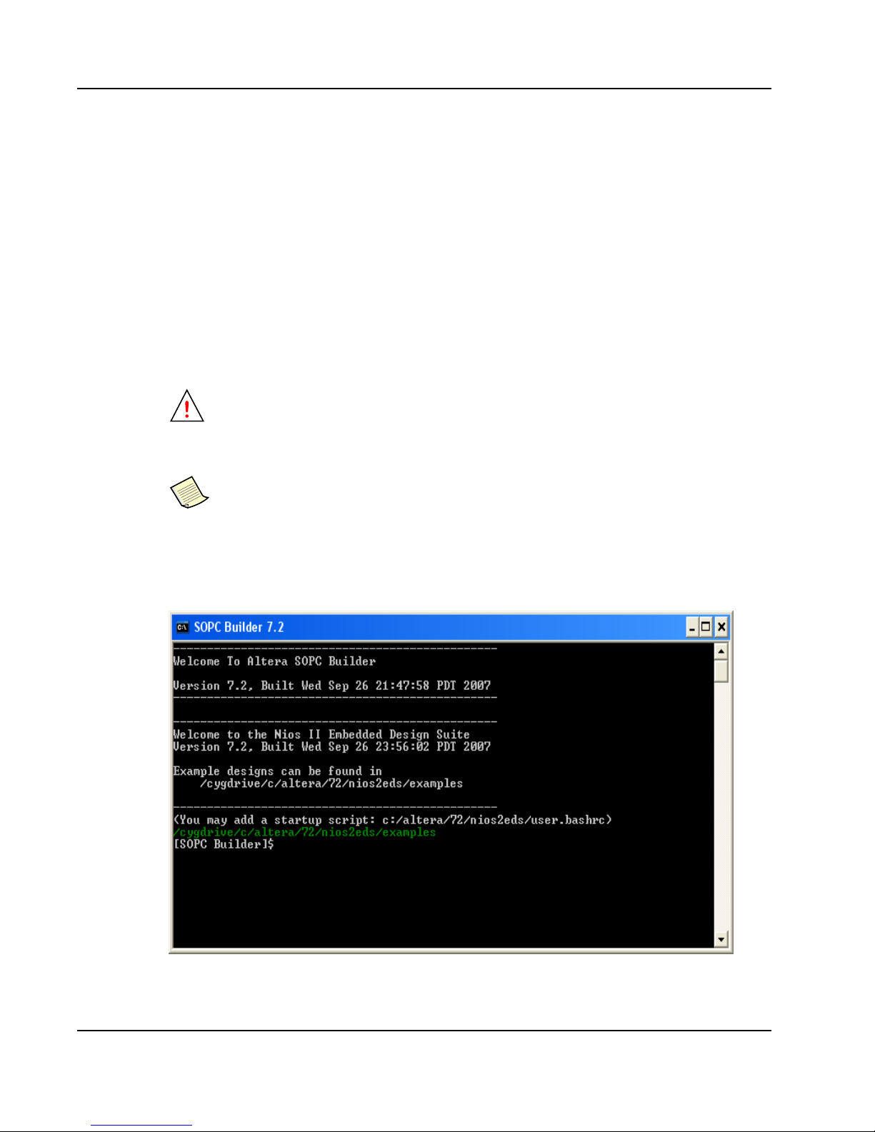
46
• altera_stratix_3_srio_3125_x1_zip - Single lane RapidIO Interface, operating at 156.25 MHz DDR
• altera_stratix_3_srio_1250_x4_zip - Four lane RapidIO Interface, operating at 62.5 MHz DDR
2.2.1 Installing the FPGA Software
In order to run the FPGA software, it is necessary to install the following software from
www.altera.com:
• Quartus Version 7.2 or later
• Megacore 7.2 or later
• NIOS II 7.2 IDE or later
Once the Altera software is installed, create the directory which should contain all of the Alter FPGA
loads and unpack the FPGA_loads.zip file into this directory.
Due to restrictions on the Altera software, the directory path must not have any spaces.
Correct example: c:/my_fpga_loads
Incorrect example: c:/my fpga loads/temp
Instructions for the NIOS II 7.2 IDE are used below. Future versions of the IDE may require
different actions.
Next, launch the a NIOS II Command Shell by selecting START->All Programs->Altera->NIOS II
EDS 7.2->NIOS II 7.2 Command Shell. This should create a window like the one shown in Figure 13.
Figure 13: NIOS II Command Shell Window
Tsi620 Evaluation Board User Manual
60D7000_MA001_03
Intergrated Device Technology
www.idt.com
Page 47
This command window supports Unix/Linux like commands for file system navigation, including cd
Tip
(change directory), pwd (print working directory), and file name completion by selecting the “Tab
Right” key. Using these commands, go to the directory of the FPGA configuration you would like to
run. You will need to execute the following commands to configure the software load:
• cd software_bsp
• The only file in software_bsp should be create-this-bsp. Execute this file by
typing ./create-this-bsp. This command configures and generates the Board Support
Package software based on the Altera software libraries.
The BSP software files are generated based on the Altera hardware configuration.
Do not modify the BSP software files after they have been generated.
The “system.h” file found in the software_bsp directory of all configurations gives definitions
for the base address and size of all hardware components and registers found in the FPGA
hardware configuration.
• cd ../software_app
• There should be nine files in /software_app:
– create-this-app
47
– srio_main_full.c
– srio_regs.h
– cmdFPGA.c
– cmdFPGA.h
– cmdRioDma.c
– cmdRioDma.h
–cmdBase.c
–cmdBase.h
• Execute create-this-app by typing ./create-this-app. This command configures the
makefile and other supporting files for the software application which the user has written. The
makefile will compile and link the users software application and the BSP to create an executable
file named srio_test.elf.
The command sequence above must be repeated for each hardware configuration that will be
used.
Once the software has been created, a NIOS II IDE project must be created by importing the user’s
software application as follows:
1. Launch the NIOS II IDE tool
2. Under the File menu, select Import. An Import dialog window will pop up.
3. In the Import dialog window, select “Existing NIOS II software build tools project or folder into
workspace”.
Intergrated Device Technology
www.idt.com
Tsi620 Evaluation Board User Manual
60D7000_MA001_03
Page 48

48
4. Select Next >.
The Import dialog window changes to “Import NIOS II Project from File System” dialog box.
5. In the “Project contents:” text box, select the software_app directory of the hardware configuration
you want to run.
6. In the “Project Name:” text box, give the software project a unique name.
This document assumes the project name is “srio_1250_x4”.
7. Select “Next >”.
The software project should now be created.
You are now ready to run the software.
2.2.2 Running the FPGA Software
The NIOS II IDE is used to run the FPGA software. The NIOS II IDE supports multiple debug
facilities and an integrated console to allow users to debug and interact with the software. It requires
the use of a JTAG cable, preferably the Altera USB-Blaster Download Cable, which is available from
Altera Corporation (see www.altera.com). Connect the USB side of the cable to your PC, then connect
the JTAG side of the cable as shown in the Altera USB-Blaster Download Cable User Guide.
The location of the “Pin 1” stripe on the cable must match the location of the “Pin 1” dot on
the Tsi620 evaluation board.
Before executing the FPGA software, the FPGA hardware load must be programmed into the FPGA as
follows:
1. In the “Tools” pull-down menu, select “Quartus II programmer”.
The Quartus II Programmer dialog box pops up.
2. If the USB-Blaster Download Cable is not selected in the “Hardware Setup” dialog window, select
the “Hardware Setup” button and then select the USB Blaster hardware.
3. Use the “Auto Detect” button to find the devices in the JTAG chain.
This should find two devices, the second of which is the Stratix III device labelled EP3SL150.
4. Select the Stratix III device, then select “Change File”.
A dialog box will pop up.
5. Navigate to the directory that contains the hardware configuration you want to execute, then select
the file named “srio_1250_x4.sof”.
The “.sof” indicates that this is an FPGA hardware configuration file. Other hardware
configurations have similarly named files, all ending in “.sof”.
Tsi620 Evaluation Board User Manual
60D7000_MA001_03
Intergrated Device Technology
www.idt.com
Page 49

49
6. Ensure the “Program/Configure” check box is selected for the Stratix III device file.
7. Select Start.
The Stratix III device will be programmed.
Software can be downloaded and executed only when the FPGA hardware load is programmed. To
download and execute the software load, complete the following:
1. Select “Run” from the “Run” pull-down menu.
This displays up the “Create, manage, and run configurations” dialog window.
2. Select the “Nios II Hardware” option in the dialog window, and then select the “New Hardware
Configuration” button in the upper left-hand corner of the dialog box.
This creates a hardware configuration named “New Configuration” below the “Nios II Hardware”
heading.
3. Select the “New Configuration” item that was just created.
4. In the “SOPC Builder System PTF File” entry text box, use the “Browse” button to select the PTF
file associated with the FPGA hardware configuration you have programmed. The
“srio_1250_x4_sys.ptf” file is found in the same directory as the “srio_1250_x4.sof” hardware
configuration file.
5. In the “Project” text box, select “Browse” and then select the software project name
(srio_1250_x4) which matches the FPGA hardware load.
When the software project is selected, the “NIOS II ELF Executable” text box is filled in with
“srio_test.elf”.
6. Change the name of the configuration from “New Configuration” to a unique hardware/software
configuration name, such as “srio_1250_x4_config”.
7. Select “Run”.
The software is downloaded, and begins execution. Once the software/hardware configuration has
been created, the configuration can be selected to execute or debug the software load.
2.2.3 FPGA Hardware Load Facilities
The FPGA hardware load has the following facilities:
• RapidIO packet sink memory, 16 KB in size, connected to the RapidIO Avalon Master
packet sink memory is the target for NREAD and NWRITE RapidIO request packets received by
the FPGA. The NIOS II processor accesses the RapidIO packet sink memory using the Remote
Read DMA engine or the Remote Write DMA engine.
• A Remote Read DMA engine, connected to the 16 KB RX_MEMORY. The Remote Read DMA
engine is used to generate NREAD requests. Addresses and packet types are controlled by the
RapidIO Avalon Slave configuration
0x80000.
1
. The processor can access RX_MEMORY starting at address
1
. The
1. For more information on the RapidIO Avalon Master or Slave, see the RapidIO MegaCore Function User Guide available at
www.altera.com.
Intergrated Device Technology
www.idt.com
Tsi620 Evaluation Board User Manual
60D7000_MA001_03
Page 50

50
• A Remote Write DMA engine, connected to the 64KB TX_MEMORY. The Remote Write DMA
engine is used to generate NWRITE, NWRITE_R, or SWRITE requests. Addresses and packet
1
types are controlled by the RapidIO Avalon Slave configuration
. The processor can access
TX_MEMORY starting at address 0x60000.
• Maintenance Avalon Slave and Maintenance Avalon Master modules for reception and origination
of Maintenance Read and Write transactions.
• A NIOS II Processor with 128 KB of memory for the storage and execution of a software load. The
NIOS II processor can access all control registers for the functions listed above, and the
TX_MEMORY and RX_MEMORY.
The NIOS II processor cannot access the packet sink memory. The only way for the NIOS II
processor to access the packet sink memory is for the Remote Read DMA engine to copy
packet sink memory to the RX_MEMORY. This can be done using the following commands:
• REMDEST – Set the remote destination ID to match the destination ID of the FPGA. The
FPGA’s destination ID is found in a register at offset 0x60
• REMRD – Copy the packet sink memory into the RX_MEMORY.
• MEM – Display the RX_MEMORY contents copied from the packet sink memory
2.2.4 Software Environment
The software environment begins execution by displaying the following:
• The environment
• The list of available commands
• The syntax for the “?” command, which displays information about commands in the environment.
For more information on a command and its syntax, use “? <cmd> FULL”.
Typically, the following command sequence is used:
1. INIT – To initialize the RapidIO masters and slaves
2. MNIT and MEM commands – To initialize and display the TX_MEMORY and RX_MEMORY
3. GET and LOAD commands – To read and write hardware registers and memory
4. RMR and RMW commands – To verify RapidIO connectivity to the Tsi620 and other RapidIO
devices.
1
.
5. REMDEST – To set the Destination ID for the REMRD and REMWR commands
6. REMRD and REMWR commands – To read and write memory on RapidIO devices
Tsi620 Evaluation Board User Manual
60D7000_MA001_03
Intergrated Device Technology
www.idt.com
Page 51

2.2.4.1 Software Implementation Structure
The main routine of the executable is found in the srio_main_full.c file. This consists of a single
routine that initializes the command base, binds FPGA and DMA related commands into the command
base, and then executes the main command loop.
The cmdBase.c and cmdBase.h files implement the command base, which consists of the following:
• Command interpreter initialization and main loop
• Mechanism for binding commands into the command interpreter
• “QUIT” command to exit the command interpreter
• “?” command
• Parameter parsing utilities
• Syntax error display facility
The cmdFPGA.c and cmdFPGA.h files implement basic FPGA commands:
• GET and LOAD
• RMR and RMW
• RMSOAK
51
•INIT
• RESET
• MEM and MNIT
The cmdRioDma.c and cmdRioDma.h files implement DMA-related FPGA commands:
•REMDEST
• REMRD, REMWR
•REMSOAK
2.3 DSP Software
The DSP software consists of a simple application that interacts with the PMC software. The DSP also
supports a large amount of memory that can act as a target for transfers to and from the FPGA/PMC.
2.3.1 Installing the DSP Software
In order to execute the DSP software, the Texas Instruments Code Composer Studio (CCS) application
must be used (for information on the application’s installation and use, see www.ti.com). CCS needs a
Blackhawk emulator to physically transfer data from CCS to the DSP hardware (for information on
ordering a Blackhawk emulator, see www.blackhawk-dsp.com).
IDT recommends the purchase of the Blackhawk “Bus-powered USB560 JTAG emulator”
product. This emulator requires a 14-pin to 60-pin converter module from Blackhawk, model
number BH-14e_TI-60t_TI.
Intergrated Device Technology
www.idt.com
Tsi620 Evaluation Board User Manual
60D7000_MA001_03
Page 52

52
The source code for the demo software can be installed to a directory of your choice. If you choose to
re-compile the software, you must install the Chip Support Library (CSL) available from Texas
Instruments. The precompiled image included on the disk was compiled with CSL version 10, although
newer versions of the software should also work.
2.3.2 Running the DSP Software
To execute the software, first connect the Blackhawk emulation pod to the Tsi620 evaluation board
connector. The 60-pin connector is not keyed, however once the Blackhawk emulator and adapter are
installed, a correctly oriented cable will have the lead pointing toward the FPGA fan.
On your PC, perform the following steps to run the DSP software:
1. Launch Code Composer Studio Setup.
2. Select “File->Import” and browse to the Tsi620EVB.ccs file found on the CD in the “DSP”
directory.
This configures CCS and the Blackhawk emulator to use the 3-core DSP mounted on the Tsi620
evaluation board.
3. Click “Save and Quit” and launch Code Composer Studio.
The “CCStudio: Parallel Debug Manager” window appears with four entries: ICEPICK_C_0,
C6400PLUS_0, C6400PLUS_1, and C6400PLUS_2. The C6400PLUS entries represent the three
cores in the TI 6487 DSP.
4. Right-click on C6400PLUS_0 and select “Connect”.
5. Double-click on C6400PLUS_0 to enter CCStudio using Core 0.
6. From the “File” menu, select “Load Program”.
7. Select the file “DSPDemo.out” located on the disc.
This programs the DSP from the precompiled file.
8. From the “Debug” menu, select “run”.
The DSP is now executing code, and waiting for interaction from the PowerPC
2.3.3 DSP Hardware Facilities
DSP hardware that is accessible from other devices includes L2 cache memory on each of the three
DSP cores. These memory addresses can be accessed from RapidIO using I/O transactions beginning at
offset 0x10800000 for core 0, 0x20800000 for core 1, and 0x30800000 for core 2. Each core can access
its local L2 cache as address 0x00800000.
The DSP hardware also supports RapidIO Doorbell functionality, although this is not covered by the
demo software or by this document (for more information, Texas Instruments documentation).
Tsi620 Evaluation Board User Manual
60D7000_MA001_03
Intergrated Device Technology
www.idt.com
Page 53

2.4 PMC/DSP/FPGA Software Execution
To execute the PMC software at the same time as the DSP and FPGA software, the following order of
software execution must be used:
1. After the Tsi620 evaluation board is powered up, the DSP and FPGA software must be started
before the PMC software can be started.
The correct Tsi620 configuration must be programmed into the EEPROM. The board must
then be reset before the DSP or PMC software can be executed.
To program the correct Tsi620 configuration, use the IDT JTAG Register Access Software
Tool for the “Tsi” RapidIO switches and the “altWSPD.txt” file to program the Tsi620
EEPROM, where:
• W – FPGA interface width, either 4 or 1
• SPD – FPGA interface speed, either 125, 250, or 3125
2. The FPGA “INIT” command must be executed before the PMC software can be started.
53
Intergrated Device Technology
www.idt.com
Tsi620 Evaluation Board User Manual
60D7000_MA001_03
Page 54

54
Tsi620 Evaluation Board User Manual
60D7000_MA001_03
Intergrated Device Technology
www.idt.com
Page 55

CORPORATE HEADQUARTERS
6024 Silver Creek Valley Road
San Jose, CA 95138
for SALES:
800-345-7015 or 408-284-8200
fax: 408-284-2775
www.idt.com
for Tech Support:
408-360-1533
sRIO@idt.com
Document: 60D7000_MA001_03
August 7, 2009
 Loading...