

Page 1

IDT Tsi572
Titl
Serial RapidIO Switch
Hardware Manual
May 18, 2012
Page 2

Integrated Device Technology, Inc. (“IDT”) reserves the right to make changes to its products or specifications at any time, without notice, in order to improve design or
performance. IDT does not assume responsibility for use of any circuitry described herein other than the circuitry embodied in an IDT product. Disclosure of the information
herein does not convey a license or any other right, by implication or otherwise, in any patent, trademark, or other intellectual property right of IDT. IDT products may
contain errata which can affect product performance to a minor or immaterial degree. Current characterized errata will be made available upon request. Items identi fied
herein as “reserved” or “undefined” are reserved for future definition. IDT does not assume responsibility for conflicts or incompatibilities arising from the future definition
of such items. IDT products have not been designed, tested, or manufactured for use in, and thus are not warranted for, applications where the failure, malfunction, or
any inaccuracy in the application carries a risk of death, serious bodily injury, or damage to tangible property. Code examples provided herein by IDT are for illustrative
purposes only and should not be relied upon for developing applications. Any use of such code examples shall be at the user's sole risk.
Copyright © 2012 Integrated Device Technology, Inc.
All Rights Reserved.
The IDT logo is registered to Integrated Device Technology, Inc. IDT and CPS are trademarks of Integrated Device Technology, Inc.
GENERAL DISCLAIMER
Page 3

Contents
1. Signals and Package . . . . . . . . . . . . . . . . . . . . . . . . . . . . . . . . . . . . . . . . . . . . . . . . . 9
1.1 Pinlist . . . . . . . . . . . . . . . . . . . . . . . . . . . . . . . . . . . . . . . . . . . . . . . . . . . . . . . . . . . . . . . . . . . . . . . 9
1.2 Signals . . . . . . . . . . . . . . . . . . . . . . . . . . . . . . . . . . . . . . . . . . . . . . . . . . . . . . . . . . . . . . . . . . . . . 10
1.3 Package Characteristics . . . . . . . . . . . . . . . . . . . . . . . . . . . . . . . . . . . . . . . . . . . . . . . . . . . . . . . . 24
1.4 Thermal Characteristics . . . . . . . . . . . . . . . . . . . . . . . . . . . . . . . . . . . . . . . . . . . . . . . . . . . . . . . . 27
2. Electrical Characteristics . . . . . . . . . . . . . . . . . . . . . . . . . . . . . . . . . . . . . . . . . . . . 29
2.1 Absolute Maximum Ratings. . . . . . . . . . . . . . . . . . . . . . . . . . . . . . . . . . . . . . . . . . . . . . . . . . . . . 29
2.2 Recommended Operating Conditions. . . . . . . . . . . . . . . . . . . . . . . . . . . . . . . . . . . . . . . . . . . . . . 30
2.3 Power . . . . . . . . . . . . . . . . . . . . . . . . . . . . . . . . . . . . . . . . . . . . . . . . . . . . . . . . . . . . . . . . . . . . . . 31
2.4 Electrical Characteristics . . . . . . . . . . . . . . . . . . . . . . . . . . . . . . . . . . . . . . . . . . . . . . . . . . . . . . . 34
3. Layout Guidelines . . . . . . . . . . . . . . . . . . . . . . . . . . . . . . . . . . . . . . . . . . . . . . . . . . 41
3.1 Overview . . . . . . . . . . . . . . . . . . . . . . . . . . . . . . . . . . . . . . . . . . . . . . . . . . . . . . . . . . . . . . . . . . . 41
3.2 Impedance Requirements . . . . . . . . . . . . . . . . . . . . . . . . . . . . . . . . . . . . . . . . . . . . . . . . . . . . . . . 41
3.3 Tracking Topologies. . . . . . . . . . . . . . . . . . . . . . . . . . . . . . . . . . . . . . . . . . . . . . . . . . . . . . . . . . . 42
3
3.4 Power Distribution . . . . . . . . . . . . . . . . . . . . . . . . . . . . . . . . . . . . . . . . . . . . . . . . . . . . . . . . . . . . 55
3.5 Decoupling Requirements . . . . . . . . . . . . . . . . . . . . . . . . . . . . . . . . . . . . . . . . . . . . . . . . . . . . . . 57
3.6 Clocking and Reset. . . . . . . . . . . . . . . . . . . . . . . . . . . . . . . . . . . . . . . . . . . . . . . . . . . . . . . . . . . . 61
3.7 Modeling and Simulation . . . . . . . . . . . . . . . . . . . . . . . . . . . . . . . . . . . . . . . . . . . . . . . . . . . . . . . 65
3.8 Testing and Debugging Considerations . . . . . . . . . . . . . . . . . . . . . . . . . . . . . . . . . . . . . . . . . . . . 66
3.9 Reflow Profile. . . . . . . . . . . . . . . . . . . . . . . . . . . . . . . . . . . . . . . . . . . . . . . . . . . . . . . . . . . . . . . . 69
A. Clocking . . . . . . . . . . . . . . . . . . . . . . . . . . . . . . . . . . . . . . . . . . . . . . . . . . . . . . . . . . 71
A.1 Line Rate Support. . . . . . . . . . . . . . . . . . . . . . . . . . . . . . . . . . . . . . . . . . . . . . . . . . . . . . . . . . . . . 71
A.2 P_CLK Programming. . . . . . . . . . . . . . . . . . . . . . . . . . . . . . . . . . . . . . . . . . . . . . . . . . . . . . . . . . 75
B. Ordering Information . . . . . . . . . . . . . . . . . . . . . . . . . . . . . . . . . . . . . . . . . . . . . . . . 87
B.1 Ordering Information . . . . . . . . . . . . . . . . . . . . . . . . . . . . . . . . . . . . . . . . . . . . . . . . . . . . . . . . . . 87
B.2 Part Numbering Information . . . . . . . . . . . . . . . . . . . . . . . . . . . . . . . . . . . . . . . . . . . . . . . . . . . . 87
Integrated Device Technology
www.idt.com
Tsi572 Hardware Manual
May 18, 2012
Page 4

4
Tsi572 Hardware Manual
May 18, 2012
Integrated Device Technology
www.idt.com
Page 5
About this Document
This section discusses general document information about the Tsi572. The following topics are
described:
• “Scope” on page 5
• “Document Conventions” on page 5
• “Revision History” on page 6
Scope
The Tsi572 Hardware Manual discusses electrical, physical, and board layout information for
the Tsi572. It is intended for hardware engineers who are designing system interconnect
applications with these devices.
5
Document Conventions
This document uses a variety of conventions to establish cons istency and to help you quickly
locate information of interest. These conventions are briefly discussed in the following sections.
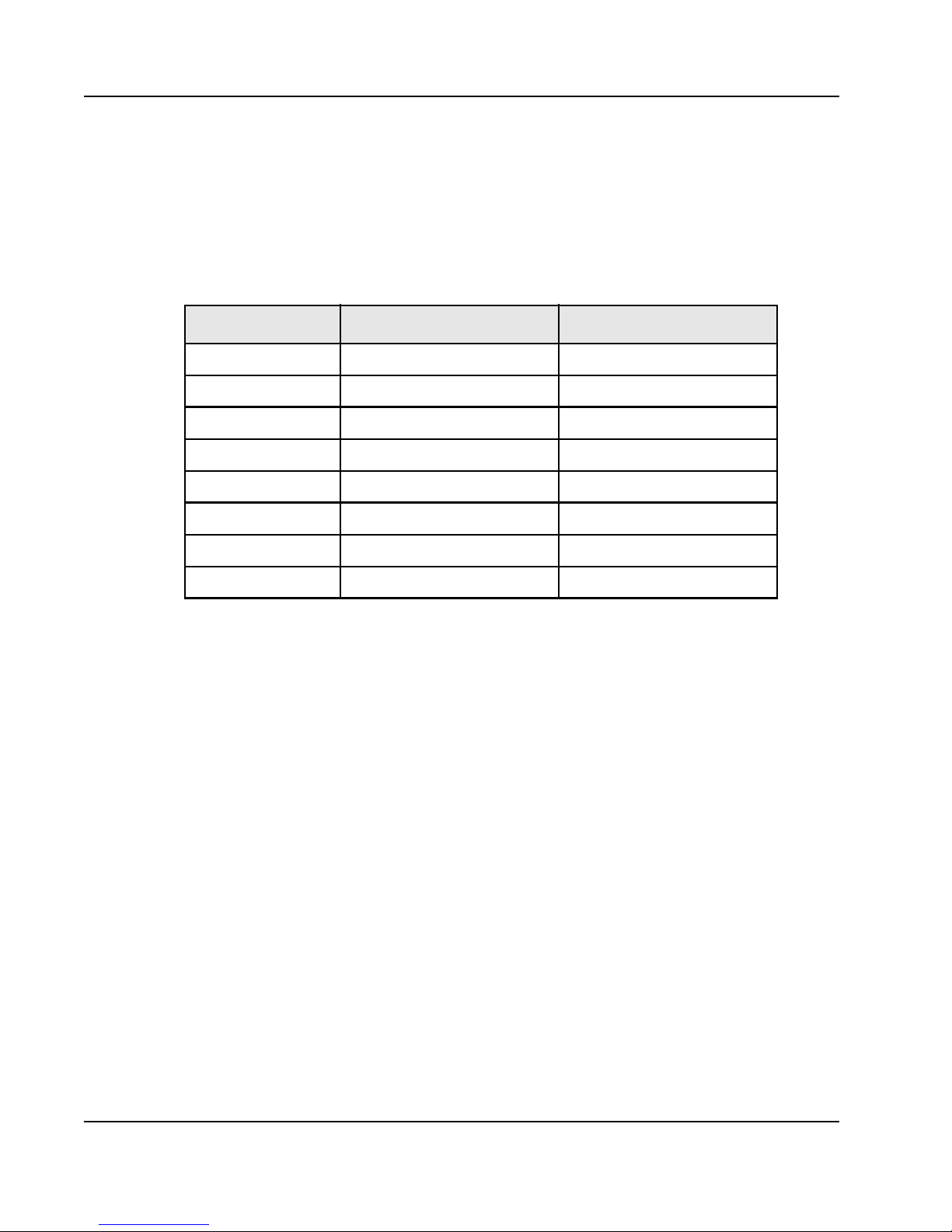
Non-differential Signal Notation
Non-differential signals are either active-low or active-high. An active-low signal has an active
state of logic 0 (or the lower voltage level), and is denoted by a lowercase “b”. An active-high
signal has an active state of logic 1 (or the higher voltage l evel ), an d is not denoted by a special
character. The following table illustrates the non-differential signal naming convention.
State Single-line signal Multi-line signal
Active low NAME_b NAMEn[3]
Active high NAME NAME[3]
Integrated Device Technology
www.idt.com
Tsi572 Hardware Manual
May 18, 2012
Page 6
6
Tip
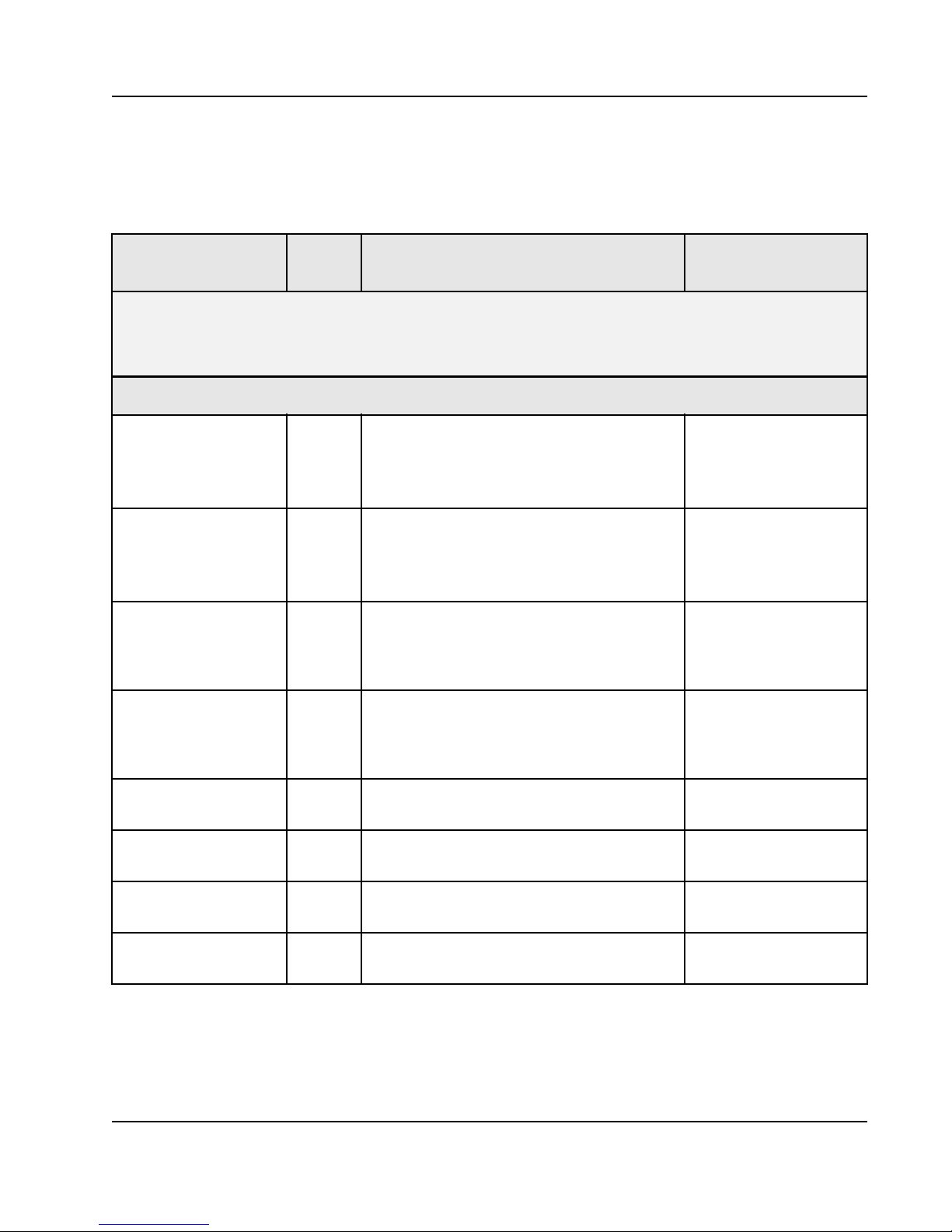
Differential Signal Notation
Differential signals consist of pairs of complement positive and negative signals that are
measured at the same time to determine a signal’s active or inactive state (they are denoted by
“_p” and “_n”, respectively). The following table illustrates the differential signal naming
convention.
State Single-line signal Multi-line signal
Inactive NAME_p = 0
Active NAME_p = 1
Symbols
This symbol indicates a basic design concept or information considered helpful.
This symbol indicates important configuration information or suggestions.
This symbol indicates procedures or operating levels that may result in misuse or
damage to the device.
Revision History
May 18, 2012, Formal
NAME_n = 1
NAME_n = 0
NAME_p[3] = 0
NAME_n[3] =1
NAME_p[3] is 1
NAME_n[3] is 0
• Updated the first paragraph in “Power Sequencing” on page 33
• Changed the SP_IO_SPEED setting in Table 21 for 125 MHz / 1.25 Baud rate to 1,1
November 18, 2010, Formal
• Added a note to Table 13
August 2009, Formal
This is the current release of the Serial RapidIO Switch. There have been no technical changes
to the document; the formatting has been updated to reflect IDT.
June 2009, Formal
Changes have been implemented throughout the document.
Serial RapidIO Switch
May 18, 2012
Integrated Device Technology
www.idt.com
Page 7

July 2008, Advance
The changes to this documents includes adding industrial variants of the device to “Ordering
Information” on page 87.
June 2008, Advance
This was the first version of the Serial RapidIO Switch.
7
Integrated Device Technology
www.idt.com
Tsi572 Hardware Manual
May 18, 2012
Page 8

8
Serial RapidIO Switch
May 18, 2012
Integrated Device Technology
www.idt.com
Page 9

1. Signals and Package
This chapter describes the packaging (mechanical) features for the Tsi572. It includes the
following information:
• “Pinlist” on page 9
• “Signals” on page 10
• “Package Characteristics” on page 24
• “Thermal Characteristics” on page 27
1.1 Pinlist
The pinlist and ballmap information for the Tsi572 are available by visiting www.idt.com. For
more information, see the following documents:
9
• Tsi572 Pinlist
• Tsi572 Ballmap
Integrated Device Technology
www.idt.com
Tsi572 Hardware Manual
May 18, 2012
Page 10
10
1.2 Signals
Figure 1: Signal Grouping
TCK
TDI
TDO
TMS
TRST_b
TRST_b
BCE
I2C_SCLK
I2C_SD
I2C_DISABLE
I2C_MA
I2C_SEL
I2C_SA[1,0]
MCES Multicast event
1
1
1
1
1
1
1
1
1
1
1
1
2
1
JTAG
TAP
2
I
C
Control symbol
HARD_RST_b
SW_RST_b
INT_b
1
Reset
1
1
Interrupt
Ports
4x Mode: 0
1x Mode: 0,1
Ports
4x Mode: 6
1x Mode: 6,7
Ports
1x Mode: 2,3,4,5
8
8
1
1
1
8
8
1
1
1
1
16
16
4
4
4
SP0_T[A,B,C,D]_[p,n]
SP0_R[A,B,C,D]_[p,n]
SP0_REXT
SP0_MODESEL
SP1_PWRDN
SP6_T[A,B,C,D]_[p,n]
SP6_R[A,B,C,D]_[p,n]
SP6_REXT
SP6_PWRDN
SP7_PWRDN
SP6_MODESEL
SP{2,4}_T[A,B]_[p,n]
SP{2,4}_R[A,B]_[p,n]
SP{2,4}_REXT
SP{2,4}_PWRDN
SP{3,5}_PWRDN
S_CLK_[p,n]
P_CLK
2
1
VSS
VDD
VDD _IO
REF_AVDD
2
Tsi572 Hardware Manual
May 18, 2012
Ref Clks
VSS
VDD
VDD_IO
REF_AVDD
4x Mode Lane Swap
Port
Configuration
Ports{0,2,4,6}
SP_VDD
Ports{0,2,4,6}
SP_AVDD
1
1
2
TX_SWAP
RX_SWAP
SP_IO_SPEED[1:0]
SP_VDD
SP_AVDD
Integrated Device Technology
www.idt.com
Page 11
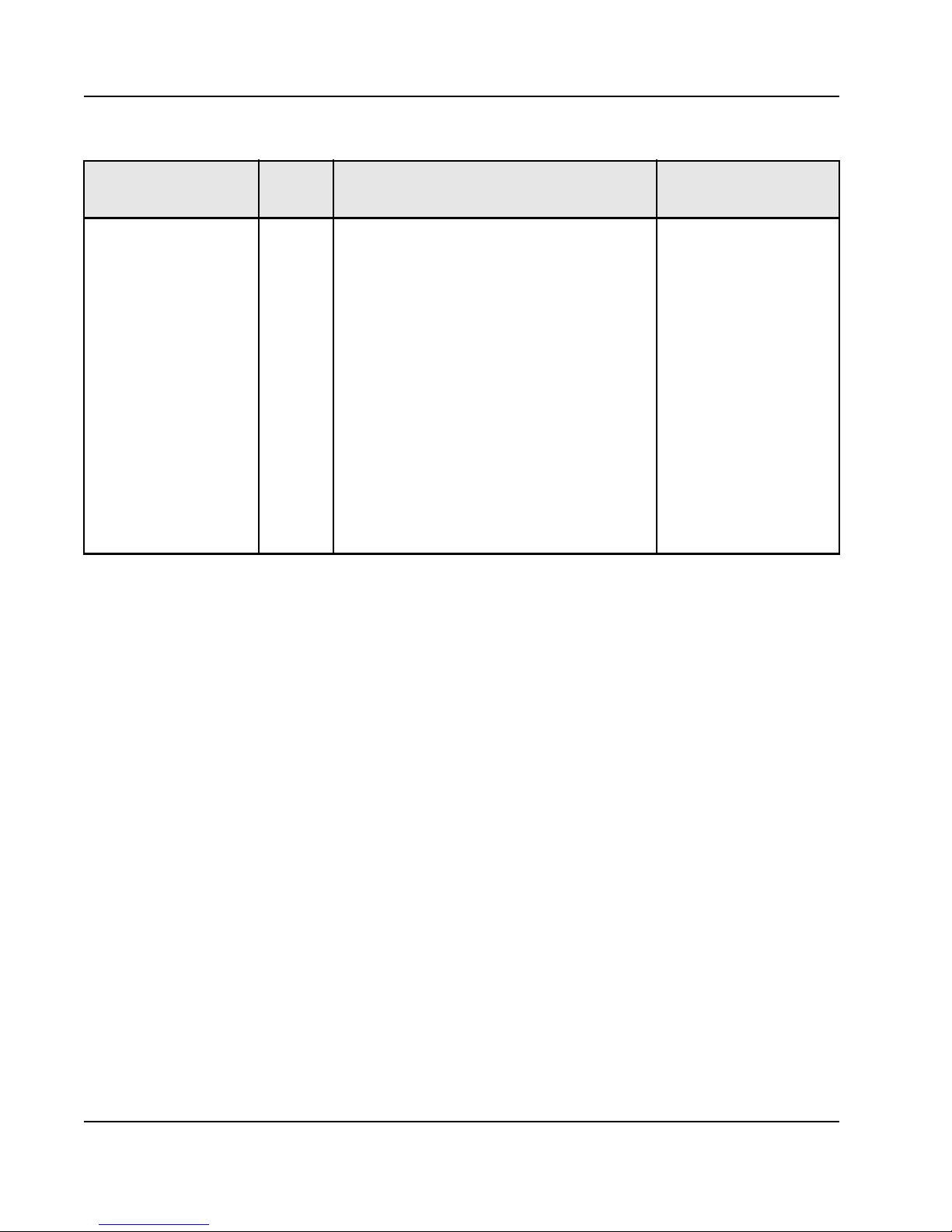
1.2.1 Conventions
The following conventions are used in the signal description table:
• Signals with the suffix “_p” are the positive half of a differential pair.
• Signals with the suffix “_n” are the negative half of a differential pair.
• Signals with the suffix “_b” are active low.
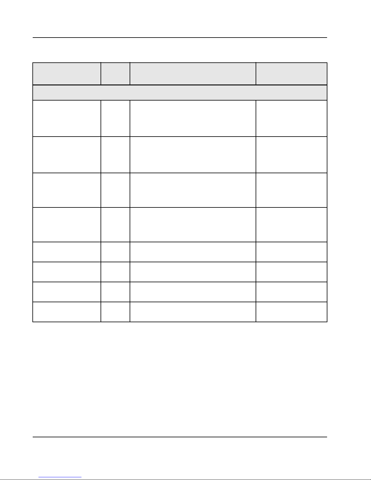
Signals are classified according to the types defined in Table 1.
Table 1: Signal Types
Pin Type Definition
I Input
O Output
I/O Input/Output
OD Open Drain
11
SRIO Differential driver/receiver defined by RapidIO
PU Pulled Up internal to the Tsi57 2
PD Pulled Down internal to the Ts i572
L VT TL CMOS I/O with LVTTL thresholds
Hyst
Core Power Core supply
Core Ground Ground for core logic
I/O Power I/O supply
N/C No connect
1.2.2 Endian Ordering
This document follows the bit-numbering convention adopted by RapidIO Interconnect
Specification (Revision 1.3), where [0:7] is used to represent an 8 bit bus with bit 0 as the
most-significant bit.
Interconnect Specification (Revision 1.3)
Hysteresis
These signals must be left unconnected.
Integrated Device Technology
www.idt.com
Tsi572 Hardware Manual
May 18, 2012
Page 12
12
1.2.3 Port Numbering
The following table shows the mapping between port numbers and the physical ports. These port
numbers are used within the destination ID lookup tables for ingress RapidIO ports and in numerous
register configuration fields.
Table 2: Port Numbering
Port Number RapidIO Port Mode
0 Serial Port 0 (SP0) 1x or 4x
1 Serial Port 1 (SP1) 1x
2 Serial Port 2 (SP2) 1x
3 Serial Port 3 (SP3) 1x
4 Serial Port 4 (SP4) 1x
5 Serial Port 5 (SP5) 1x
6 Serial Port 6 (SP6) 1x or 4x
7 Serial Port 7 (SP7) 1x
Tsi572 Hardware Manual
May 18, 2012
Integrated Device Technology
www.idt.com
Page 13
1.2.4 Signal Grouping
The following table lists the signals by group and their recommended termination.
Table 3: Signal Descriptions and Recommended Termination
13
Pin Name Type Description
Signal Port Numbering
n = 0, 2, 4, 6
Serial Port Transmit
SP{n}_TA_p O, SRIO Port n Lane A Differential Non-inverting Transmit
Data output (4x mode)
Port n Lane A Differential Non-inverting Transmit
Data output (1x mode)
SP{n}_TA_n O, SRIO Port n Lane A Differential Inverting T ransmit Data
output (4x mode)
Port n Lane A Differential Inverting Transmit Data
output (1x mode)
SP{n}_TB_p O, SRIO Port n Lane B Differential Non-inverting Transmit
Data output (4x mode)
Port n+1 Lane B Differential Non-inverting
Transmit Data output (1x mode)
Recommended
Termination
No termination required.
No termination required.
No termination required.
a
SP{n}_TB_n O, SRIO Port n Lane B Differential Inverting T ransmit Data
output (4x mode)
Port n+1 Lane B Differential Inverting Transmit
Data output (1x mode)
SP[0,6]_TC_p O, SRIO Port n Lane C Differential Non-inverting Transmit
Data output (4x mode)
SP[0,6]_TC_n O, SRIO Port n Lane C Differential Inverting Transmit Data
output(4x mode)
SP[0,6]_TD_p O, SRIO Port n Lane D Differential Non-inverting Transmit
Data output
SP[0,6]__TD_ O, SRIO Port n Lane D Differential Inverting Transmit Data
output (4x mode)
Integrated Device Technology
www.idt.com
(4x mode)
No termination required.
No termination required.
No termination required.
No termination required.
No termination required.
Tsi572 Hardware Manual
May 18, 2012
Page 14
14
Table 3: Signal Descriptions and Recommended Termination
Pin Name Type Description
Serial Port Receive
SP{n}_RA_p I, SRIO Port n Lane A Differential Non-inverting Receive
Data input (4x node)
Port n Lane A Differential Non-inverting Receive
Data input (1x mode)
SP{n}_RA_n I, SRIO Port n Lane A Differential Inverting Receive Data
input (4x mode)
Port n Lane A Differential Inverting Receive Data
input (1x mode)
SP{n}_RB_p I, SRIO Port n Lane B Differential Non-inverting Receive
Data input (4x mode)
Port n+1 Lane B Differential Non-inverting
Receive Data input (1x mode)
SP{n}_RB_n I, SRIO Port n Lane B Differential Inverting Receive Data
input (4x mode)
Port n+1 Lane B Differential Inverting Receive
Data input (1x mode)
Recommended
Termination
a
DC blocking capacitor of
0.1uF in series
DC blocking capacitor of
0.1uF in series
DC blocking capacitor of
0.1uF in series
DC blocking capacitor of
0.1uF in series
SP[0,6]_RC_p I, SRIO Port n Lane C Differential Non-inverting Receive
Data input(4x mode)
SP[0,6]_RC_n I, SRIO Port n Lane C Differential Inverting Receive Data
input (4x mode)
SP[0,6]_RD_p I, SRIO Port n Lane D Differential Non-inverting Receive
Data input(4x mode)
SP[0,6]_RD_n I, SRIO Port n Lane D Differential Inverting Receive Data
input (4x mode)
DC blocking capacitor of
0.1uF in series
DC blocking capacitor of
0.1uF in series
DC blocking capacitor of
0.1uF in series
DC blocking capacitor of
0.1uF in series
Tsi572 Hardware Manual
May 18, 2012
Integrated Device Technology
www.idt.com
Page 15
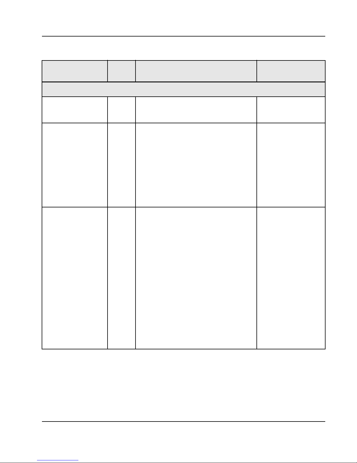
Table 3: Signal Descriptions and Recommended Termination
15
Pin Name Type Description
Serial Port Configuration
SP{n}_REXT Analog Used to connect a resistor to VSS to provide a
reference current for the driver and equalization
circuits.
SP{n}_MODESEL I/O,
LVTTL,
PD
Selects the serial port operating mode for ports
0and 6
0 = Port 0 or 6 operating in 4x mode
1 = Ports n and n+1 operating in 1x mode
Note: Output capability of this pin is only used in
test mode.
Must remain stable for 10 P_CLK cycles after
HW_RST_b is de-asserted in order to be sampled
correctly.
This signal is ignored after reset.
SP{n}_PWRDN I/O,
LVTTL,
PU
Port n Transmit and Receive Power Down control
This signal controls the state of Port n and Port
n+1
The PWRDN controls the state of all four lanes
(A/B/C/D) of SERDES Macro.
0 = Port n Powered Up. Port n+1 controlled by
SP{n+1}_PWRDN.
1 = Port n Powered Down. Port n+1 Powered
Down.
Override SP{n}_PWRDN using PWDN_x1 field in
“SRIO MAC x Clock Selection Register” in the
Tsi572 User Manual.
Output capability of this pin is only used in test
mode.
Must remain stable for 10 P_CLK cycles after
HW_RST_B is de-asserted in order to be sampled
correctly.
This signal is ignored after reset.
Recommended
Termination
a
Must be connected to VSS
with a 191-ohm (1%)
resistor.
Pin must be tied off
according to the required
configuration. Either a 10K
pull up to VDD_IO or a
10K pull-down to VSS_IO.
Internal pull-down may be
used for logic 0.
Pin must be tied off
according to the required
configuration. Either a 10K
pull up to VDD_IO or a
10K pull-down to VSS_IO.
Internal pull-up may be
used for logic 1.
Integrated Device Technology
www.idt.com
Tsi572 Hardware Manual
May 18, 2012
Page 16
16
Table 3: Signal Descriptions and Recommended Termination
Pin Name Type Description
SP{n+1}_PWRDN I/O,
LVTTL,
PU
Port n+1 Transmit and Receive Power Down
control
This signal controls the state of Port n+1. Note
that Port n+1 is never used when 4x mode is
selected for a Serial Rapid IO MAC, and it must
be powered down.
0 = Port n+1 Powered Up
1 = Port n+1 Powered Down
Override SP{n+1}_PWRDN using PWDN_x4 field
SRIO MAC x Clock Selection Register.
Output capability of this pin is only used in test
mode.
Must remain stable for 10 P_CLK cycles after
HW_RST_B is de-asserted in order to be sampled
correctly.
This signal is ignored after reset.
Recommended
Termination
a
Pin must be tied off
according to the required
configuration. Either a 10K
pull up to VDD_IO or a
10K pull-down to VSS_IO.
Internal pull-up may be
used for logic 1.
Tsi572 Hardware Manual
May 18, 2012
Integrated Device Technology
www.idt.com
Page 17
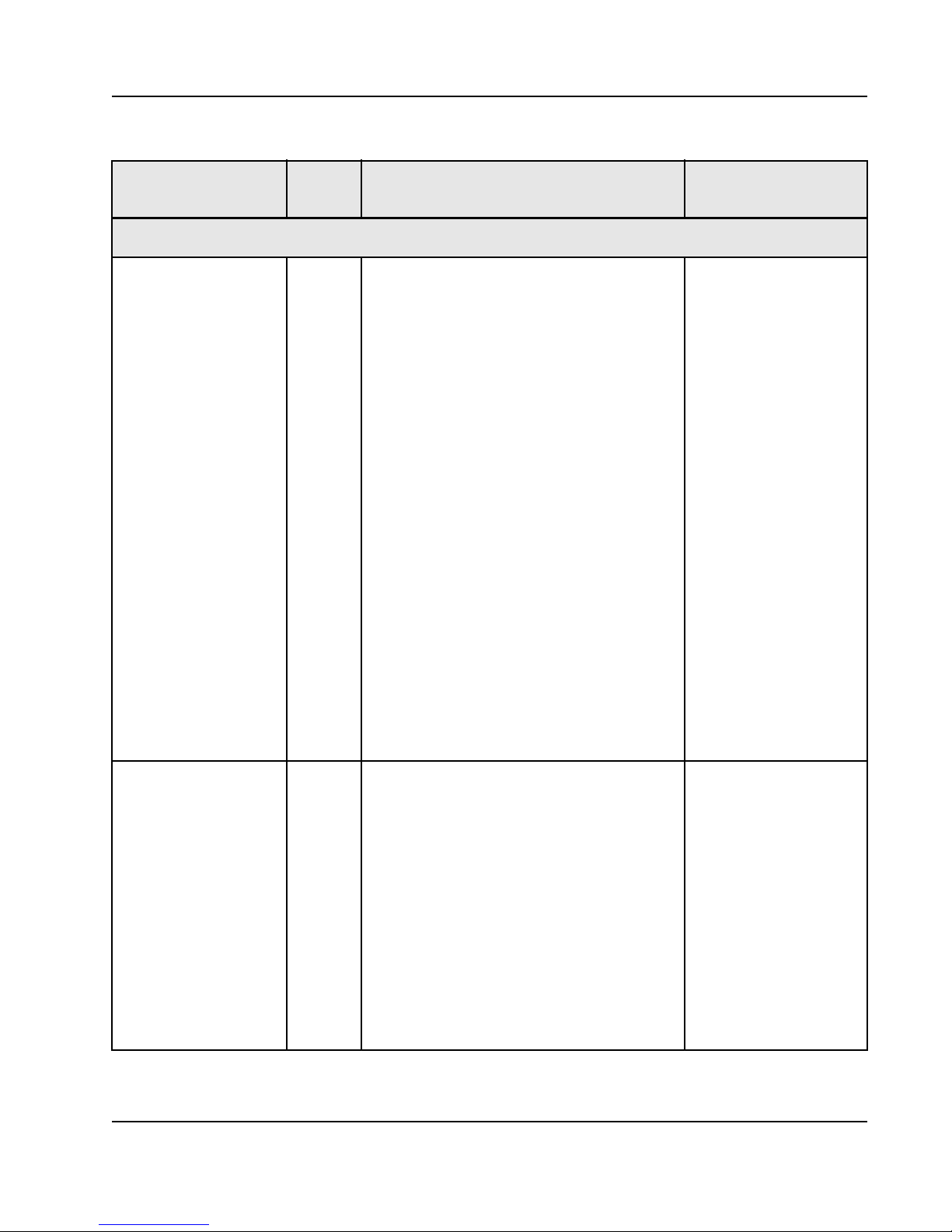
Table 3: Signal Descriptions and Recommended Termination
17
Pin Name Type Description
Serial Port Speed Select
SP_IO_SPEED[1] I/O,
LVTTL,
PU
Serial Port Transmit and Receive operating
frequency select, bit 1. When combined with
SP_IO_SPEED[0], this pin selects the default
serial port frequency for all ports.
00 = 1.25 Gbit/s
01 = 2.5 Gbit/s
10 = 3.125 Gbit/s (default)
11 = Illegal
Selects the speed at which the ports operates
when reset is removed. This could be at either
HARD_RST_b being de-asserted or by the
completion of a self-reset.
These signals must remain stable for 10 P_CLK
cycles after HW_RST_b is de-asserted in order to
be sampled correctly.
These signals are ignored after reset and
software is able to over-ride the port frequency
setting in the SRIO MAC x Digital Loopback and
Clock Selection register.
The SP_IO_SPEED[1:0] setting is equal to the
IO_SPEED field in SRIO MAC x Clock Selection
Register.
Output capability of this pin is only used in test
mode.
Recommended
Termination
a
Pin must be tied off
according to the required
configuration. Either a 10K
pull-up to VDD_IO or a
10K pull-down to VSS_IO.
Internal pull-down may be
used for logic 0.
SP_IO_SPEED[0] I/O,
LVTTL,
PD
Integrated Device Technology
www.idt.com
See SP_IO_SPEED[1] Pin must be tied off
according to the required
configuration. Either a 10K
pull-up to VDD_IO or a
10K pull-down to VSS_IO.
Internal pull-up may be
used for logic 1.
Tsi572 Hardware Manual
May 18, 2012
Page 18
18
Table 3: Signal Descriptions and Recommended Termination
Pin Name Type Description
Serial Port Lane Ordering Select
SP_RX_SWAP I, LVTTL, PDConfigures the order of 4x receive lanes on serial
ports [0,6]
0 = A, B, C, D
1 = D, C, B, A
This signal is ignored in 1X mode.
Must remain stable for 10 P_CLK cycles after
HARD_RST_b is de-asserted in order to be
sampled correctly.
This signal is ignored after reset.
Note: Ports that require the use of lane swapping
for ease of routing will only function as 4x mode
ports. The re-configuration of a swapped port to
dual 1x mode operation results in the inability to
connect to a 1x mode link partner.
SP_TX_SWAP I, LVTTL, PDConfigures the order of 4x transmit lanes on serial
ports [0,6].
0 = A, B, C, D
1 = D, C, B, A
Must remain stable for 10 P_CLK cycles after
HARD_RST_b is de-asserted in order to be
sampled correctly.
This signal is ignored after reset.
Note: Ports that require the use of lane swapping for
ease of routing only function as 4x mode ports. The
re-configuration of a swapped port to dual 1x mode
operation results in the inability to connect to a 1x
mode link partner.
Recommended
Termination
a
No termination required.
Internal pull-down can be
used for logic 0. Pull up to
VDD_IO through 10K if
external pull-up is desired.
Pull down to VSS_IO
through a 10K resistor if an
external pull-down is
desired.
No termination required.
Internal pull-down can be
used for logic 0. Pull up to
VDD_IO through 10K if
external pull-up is desired.
Pull down to VSS_IO
through 10K resistor if an
external pull-down is
desired.
Clock and Reset
P_CLK I,
LVTTL
Tsi572 Hardware Manual
May 18, 2012
This clock is used for the register bus clock.
The nominal frequency of this input clock is
100 MHz. For more information on programming
the P_CLK operating frequency, refer to “P_CLK
Programming” on page 75.
No termination required.
Integrated Device Technology
www.idt.com
Page 19
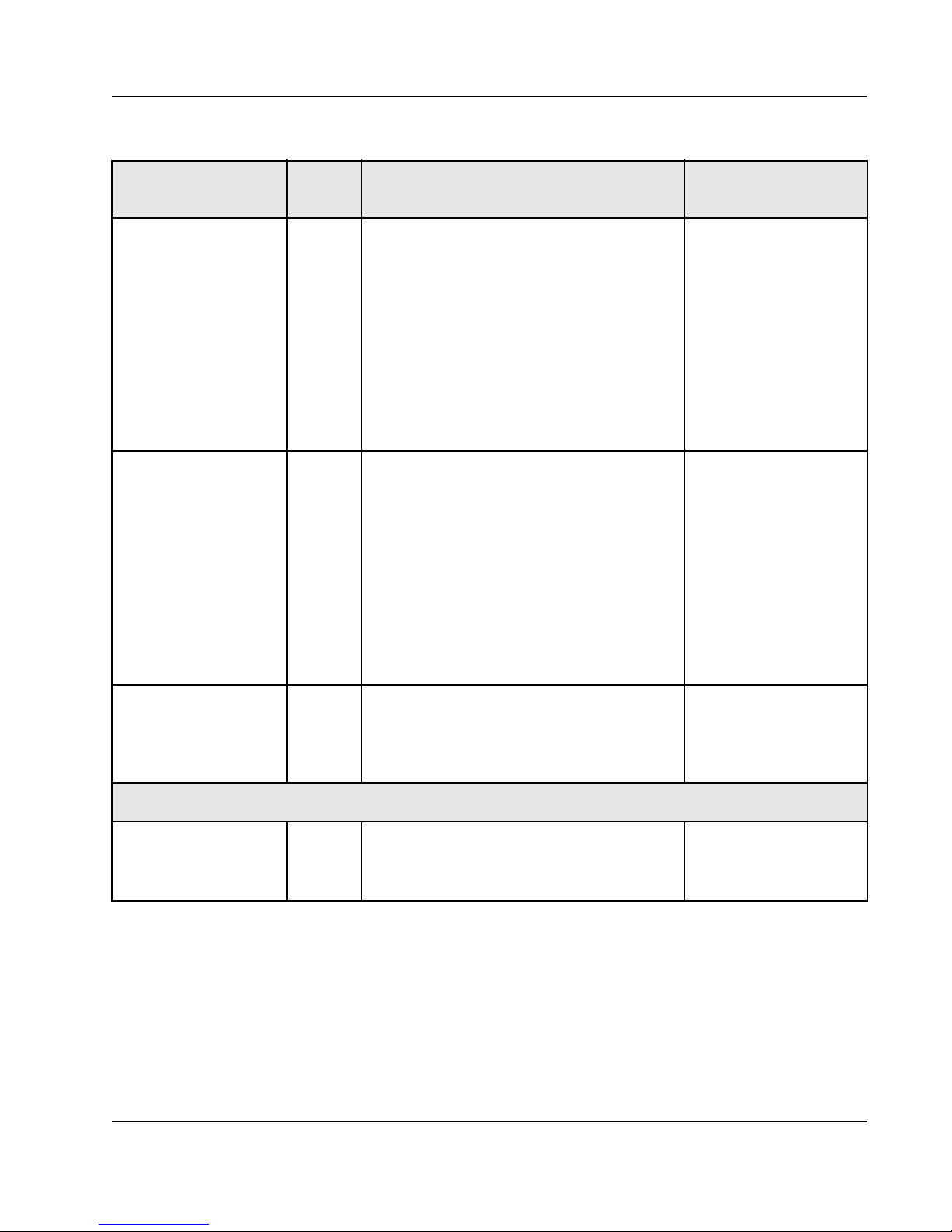
Table 3: Signal Descriptions and Recommended Termination
19
Pin Name Type Description
S_CLK_p I,
CML
Differential non-inverting reference clock. The
clock is used for following purposes: SERDES
reference clock, serial port system clock, ISF
clock and test clock.
The maximum frequency of this input clock is
156.25 MHz.
The clock frequency is defined in “Reference
Clock, S_CLK_p/n” on page 35.
For more information on the S_CLK operating
frequency, refer to “Line Rate Support” on
page 71.
S_CLK_n I,
CML
Differential inverting reference clock. The clock is
used for following purposes: SerDes reference
clock, serial port system clock, ISF clock and test
clock.
The maximum frequency of this input clock is
156.25 MHz.
The clock frequency is defined in “Reference
Clock, S_CLK_p/n” on page 35.
For more information on the S_CLK operating
frequency, refer to “Line Rate Support” on
page 71.
Recommended
Termination
a
AC coupling capacitor of
0.1uF required.
AC coupling capacitor of
0.1uF required.
HARD_RST_b I
LVTTL,
Hyst,
PU
Interrupts
INT_b O, OD,
LVTTL,
2mA
Integrated Device Technology
www.idt.com
Schmidt-triggered hard reset. Asynchronous
active low reset for the entire device.
The Tsi572 does not contain a voltage detector to
generate internal reset.
Connect to a power-up
reset source.
Refer to “Reset
Requirements” on page 64
Interrupt signal (open drain output) External pull-up required.
Pull up to VDD_IO through
a 10K resistor.
Tsi572 Hardware Manual
May 18, 2012
Page 20

20
Table 3: Signal Descriptions and Recommended Termination
Pin Name Type Description
SW_RST_b O, OD,
LVTTL,
2mA
Software reset (open drain output): This signal is
asserted when a RapidIO port receives a valid
reset request on a RapidIO link. If self-reset is not
selected, this pin remains asserted until the reset
request is cleared from the status registers. If
self-reset is selected, this pin remains asserted
until the self reset is complete. If the Tsi572 is
reset from the HARD_RST_b pin, this pin is
de-asserted and remains de-asserted after
HARD_RST_b is released.
For more information, refer to “Resets” in the
Tsi572 User’s Manual.
Multicast
MCES I/O,
LVTTL,
PD
Multicast Event Symbol pin.
As an input, an edge (rising or falling) will trigger a
Multicast Event Control Symbol will be sent to all
ports;
As an output, this pin will toggle its value every
time an Multicast Event Control Symbol is
received by any port which is enabled for
Multicast even control symbols.
Must remain stable for 10 P_CLK cycles before
and after a transition.
Recommended
Termination
a
External pull-up required.
Pull up to VDD_IO through
a 10K resistor.
No termination required.
This pin must not be driven
by an external source until
all power supply rails are
stable.
I2C
I2C_SCLK I/O, OD,
LVTTL,
PU
8mA
I2C_SD I/O, OD,
LVTTL,
PU
8mA
Tsi572 Hardware Manual
May 18, 2012
2
C input/output clock, up to 100 kHz.
I
2
If an EEPROM is present on the I
C bus, this
clock signal must be connected to the clock input
of the serial EEPROM on the I
2
C bus. If an
EEPROM is not present, the recommended
terminations should be used.
2
I
C input and output data bus (bidirectional open
drain)
No termination required.
Internal pull-up may be
used for logic 1.
Pull up to VDD_IO through
a minimum 470 ohms
resistor if higher edge rate
is required.
No termination required.
Internal pull-up may be
used for logic 1.
Pull up to VDD_IO through
a minimum 470 ohms
resistor if higher edge rate
required.
Integrated Device Technology
www.idt.com
Page 21

Table 3: Signal Descriptions and Recommended Termination
21
Pin Name Type Description
I2C_DISABLE I, LVTTL, PDDisable I2C register loading after reset. When
asserted, the Tsi572 does not attempt to load
register values from I
2
0 = Enable I
1 = Disable I
C register loading
2
2
C.
C register loading
Must remain stable for 10 P_CLK cycles after
HARD_RST_b is de-asserted in order to be
sampled correctly.
Note: This signal does not control the slave
accessibility of the interface.
This signal is ignored after reset.
I2C_MA I, CMOS, PUI
2
C Multibyte Address.
When driven high, I
2
C module will expect
multi-byte peripheral addressing; otherwise, when
driven low, single-byte peripheral address is
assumed.
Must remain stable for 10 P_CLK cycles after
HW_RST_b is de-asserted in order to be sampled
correctly.
This signal is ignored after reset.
Recommended
Termination
a
No termination required.
Pull up to VDD_IO through
a 10K resistor if I
2
C
loading is not required.
No termination required.
Internal pull-up may be
used for logic 1.
Pull up to VDD_IO through
10K resistor if an external
pull-up is desired. Pull
down to VSS_IO to
change the logic state.
I2C_SA[1,0] I, CMOS, PUI
2
C Slave Address pins.
The values on these two pins represent the
values for the lower 2 bits of the 7-bit address of
T si572 when acting as an I
2
C slave (see I2C Slave
Configuration register).
The values at these pins can be overridden by
software after reset.
No termination required.
Internal pull-up may be
used for logic 1.
Pull up to VDD_IO through
10K resistor if an external
pull-up is desired. Pull
down to VSS_IO to
change the logic state.
Integrated Device Technology
www.idt.com
Tsi572 Hardware Manual
May 18, 2012
Page 22
22
Table 3: Signal Descriptions and Recommended Termination
Recommended
Pin Name Type Description
I2C_SEL I, CMOS, PUI2C Pin Select. Together with the I2C_SA[1,0]
pins, Tsi572 will determine the lower 2 bits of the
7-bit address of the EEPROM address it boots
from.
When asserted, the I2C_SA[1,0] values will also
be used as the lower 2 bits of the EEPROM
address.
When de-asserted, the I2C_SA[1,0] pins will be
Termination
No termination required.
Internal pull-up may be
used for logic 1.
Pull up to VDD_IO through
10K resistor if an external
pull-up is desired. Pull
down to VSS_IO to
change the logic state.
a
ignored and the lower 2 bits of the EEPROM
address are default to 00.
The values of the lower 2 bits of the EEPROM
address can be over-ridden by software after
reset.
JTAG TAP Controller
TCK I, LVTTL, PDIEEE 1149.1 Test Access Port Clock input Pull up to VDD_IO through
10K resistor if not used.
TDI I, L VTTL, PUIEEE 1149.1 Test Access Port Serial Data Input Pull up to VDD_IO through
a 10K resistor if the signal
is not used or a if higher
edge rate is required.
TDO O,
LVTTL,
2mA
IEEE 1149.1 Test Access Port Serial Data Output No connect if JTAG is not
used.
Pull up to VDD_IO through
a 10K resistor if used.
TMS I, L VTTL, PUIEEE 1149.1 Test Access Port Test Mode Select Pull up to VDD_IO through
a 10K resistor if not used.
TRST_b I, LVTTL,
PU
IEEE 1149.1 Test Access Port TAP Reset Input
This input must be asserted during the assertion
Tie to VSS_IO through a
10K resistor if not used.
of HARD-RST_b. Afterwards, it may be left in
either state.
Combine the HARD_RST_b and TRST_b signals
with an AND gate and use the output to drive the
TRST_b pin.
Tsi572 Hardware Manual
May 18, 2012
Integrated Device Technology
www.idt.com
Page 23
Table 3: Signal Descriptions and Recommended Termination
23
Pin Name Type Description
BCE I, LVTTL, PUBoundary Scan compatibility enabled pin. This
input is used to aid 1149.6 testing.
This signal also enables system level diagnostic
capability using features built into the SerDes. For
more information on this functionality, refer to the
Serial RapidIO Signal Analyzer documentation.
This signal must be tied to VDD_IO during normal
operation of the device, and during JTAG
accesses of the device registers
Power Supplies
SP_AVDD - Port n and n+1: 3.3V supply for bias generator
circuitry. This is required to be a low-noise supply.
REF_AVDD - Analog 1.2V for Reference Clock (S_CLK_p/n).
Clock distribution network power supply.
Recommended
Termination
a
This signal should have
the capability to be
pulled-up or pulled-low.
• The default setting is to
be pulled-up.
• Pulling the signal low
enables the signal
analyzer functionality on
the SerDes
• A 10K resistor to
VDD_IO should be used.
Refer to ““Decoupling
Requirements” on
page 57”
Refer to ““Decoupling
Requirements” on
page 57”
Common Supply
VDD_IO - Common 3.3V supply for LVTTL I/O Refer to ““Decoupling
Requirements” on
page 57”
VSS - Common ground supply for digital logic Refer to ““Decoupling
Requirements” on
page 57”
VDD - Common 1.2V supply for digital logic Refer to ““Decoupling
Requirements” on
page 57”
SP_VDD - 1.2V supply for CDR, Tx/Rx, and digital logic for
all RapidIO ports
Refer to ““Decoupling
Requirements” on
page 57”
a. Signals for unused serial ports do not require termination and can be left as N/Cs.
Integrated Device Technology
www.idt.com
Tsi572 Hardware Manual
May 18, 2012
Page 24
24
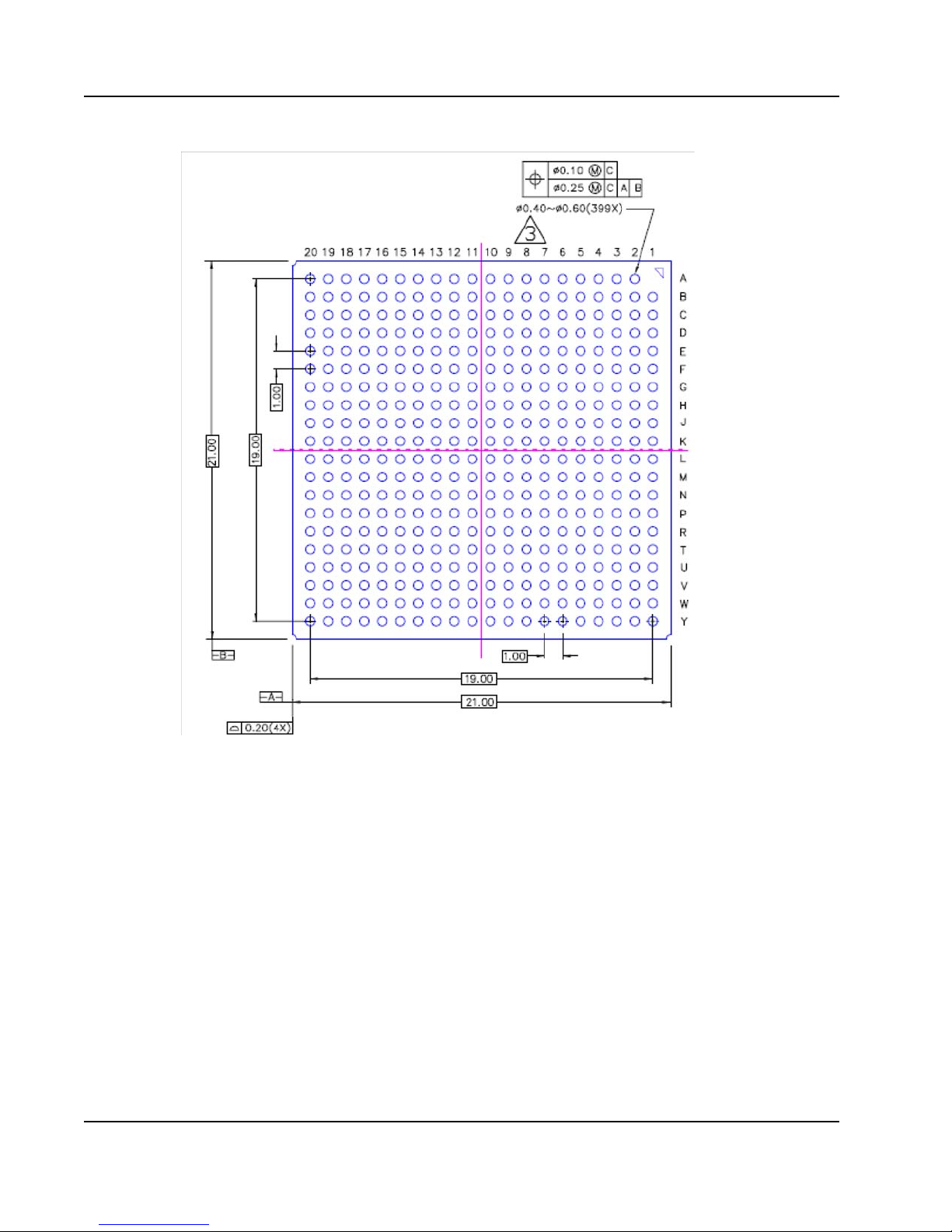
1.3 Package Characteristics
The Tsi572’s package characteristics are summarized in the following table. The following
figures show the top, side, and bottom views of the Tsi572 package.
Table 4: Package Characteristics
Feature Description
Package Type Heat Slug Ball Grid Array (HSBGA)
Package Body Size 21 mm x 21 mm
JEDEC Specification 95-1 Section 14
Pitch 1.00 mm
Ball pad size 500 um
Soldermask opening 400 um
Moisture Sensitivity Level 3
Tsi572 Hardware Manual
May 18, 2012
Integrated Device Technology
www.idt.com
Page 25
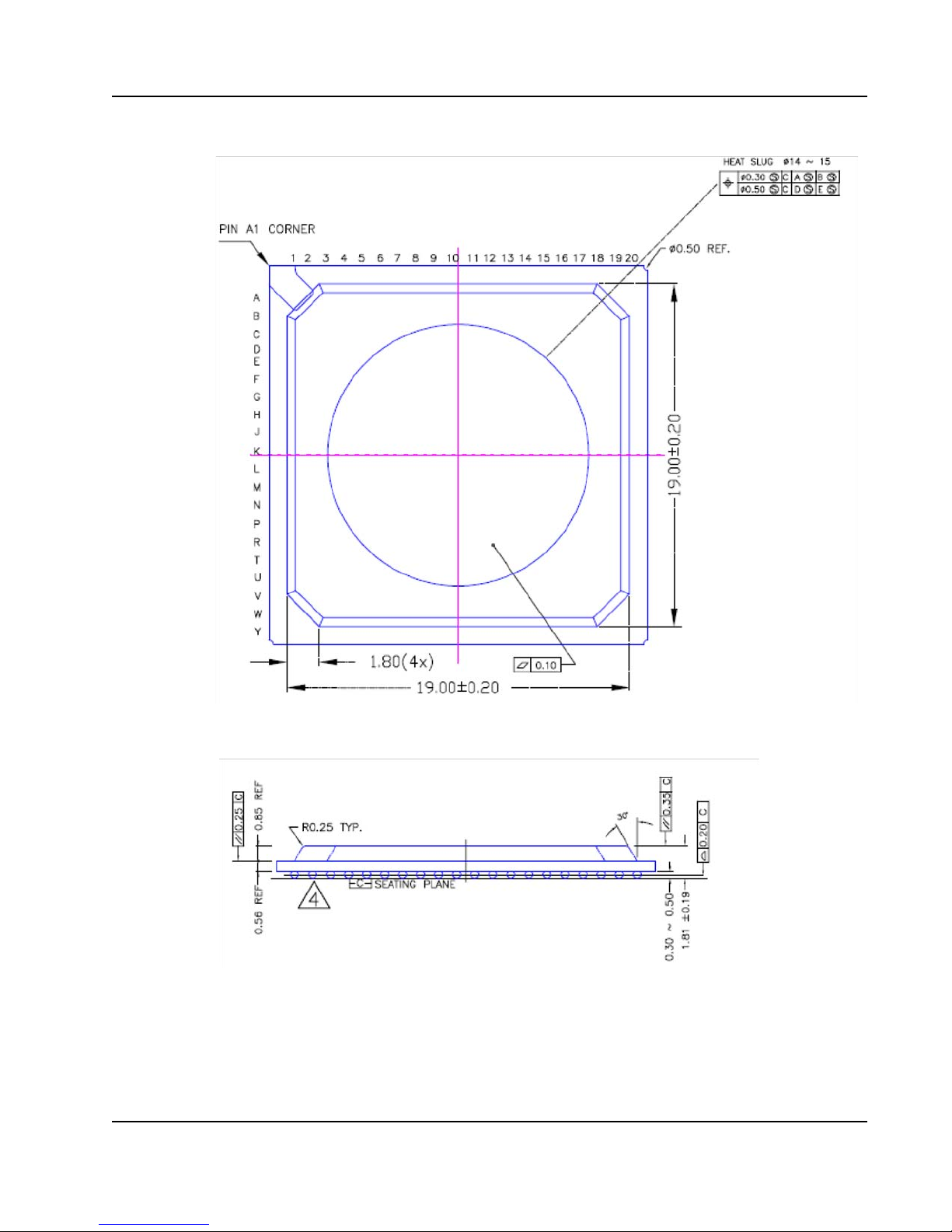
Figure 2: Package Diagram — Top View
25
Figure 3: Package Diagram — Side View
Integrated Device Technology
www.idt.com
Tsi572 Hardware Manual
May 18, 2012
Page 26
26
Figure 4: Package Diagram — Bottom View
Tsi572 Hardware Manual
May 18, 2012
Integrated Device Technology
www.idt.com
Page 27
1.4 Thermal Characteristics
Heat generated by the packaged IC has to be removed from the package to ensure that the IC is
maintained within its functional and maximum design temperature limits. If heat buildup
becomes excessive, the IC temperature may exceed the temperature limits. A consequence of
this is that the IC may fail to meet the performance specifications and the reliability objectives
may be affected.
Failure mechanisms and failure rate of a device have an exponential dependence of the IC
operating temperatures. Thus, the control of the package temperature, and by extension the
Junction Temperature, is essential to ensure product reliability. The Tsi572 is specified safe for
operation when the Junction Temperature is within the recommended limits.
27
Table 5 shows the simulated Thetajb and Theta
jc thermal characteristics of the T si572 HSBGA
package.
Table 5: Thermal Characteristics
Interface Result
Theta jb (junction to board) 9.2
Theta jc (junction to case) 4.7
C/watt
C/watt
1.4.1 Junction-to-Ambient Thermal Characteristics (Theta ja)
The following table shows the simulated Theta ja thermal characteristic of the Tsi572 HSBGA
package. The results in the table are based on a JEDEC Thermal Test Board configuration
(JESD51-9) and do not factor in system level characteristics. As such, these values are for
reference only.
The Theta ja thermal resistance characteristics of a package depend on multiple
system level variables.
Table 6: Simulated Junction to Ambient Characteristics
Package
Tsi572 HSBGA 13.0 C/watt 12.0
Integrated Device Technology
www.idt.com
Theta ja at specified airflow (no Heat Sink)
0m/s 1 m/s 2m/s
C/watt 11.4 C/watt
Tsi572 Hardware Manual
May 18, 2012
Page 28

28
1.4.1.1 System-level Characteristics
In an application, the following system-level characteristics and environmental issues must be
taken into account:
• Package mounting (vertical / horizontal)
• System airflow conditions (laminar / turbulent)
• Heat sink design and thermal characteristics
• Heat sink attachment method
• PWB size, layer count and conductor thickness
• Influence of the heat dissipating components assembled on the PWB (neighboring effects)
Example on Thermal Data Usage
Based on the Theta
data and specified conditions, the following formula can be used to derive
JA
the junction temperature (Tj) of the Tsi572 with a 0m/s airflow:
•Tj = è
P + Tamb.
JA *
Where: Tj is Junction Temperature, P is the Power consumption, Tamb is the Ambient
Temperature
Assuming a power consumption (P) of3 W and an ambient temperature (Tamb) of 70
resulting junction temperature (Tj) would be 109
C.
C, the
Tsi572 Hardware Manual
May 18, 2012
Integrated Device Technology
www.idt.com
Page 29

2. Electrical Characteristics
This chapter provides the electrical characteristics for the Tsi572. It includes the following
information:
• “Absolute Maximum Ratings” on page 29
• “Recommended Operating Conditions” on page 30
• “Power” on page 31
2.1 Absolute Maximum Ratings
Operating the device beyond the listed operating conditions is not recommended. Stressing the
Tsi572 beyond the Absolute Maximum Rating can cause permanent damage.
29
Table 7 lists the absolute maximum ratings.
Table 7: Absolute Maximum Ratings
Symbol Parameter Min Max Unit
T
storage
V
DD_IO
SP_AVDD 3.3 V Analog Supply Voltage -0.5 4.6 V
V
SP_VDD,
DD,
REF_AVDD
V
I_SP{n}-R{A-D}_{p,n}
V
O_SP{n}-T{A-D}_{p,n}
SP_AVDD Transient di/dt - 0.0917 A/nS
SP_VDD Transient di/dt - 0.136 A/nS
Storage Tempera ture -55 125 C
3.3 V DC Supply Voltage -0.5 4.6 V
1.2 V DC Supply Voltage -0.3 1.7 V
SERDES Port Receiver Input Voltage -0.3 3 V
SERDES Port VM Transmitter Output Voltage -0.3 3 V
Integrated Device Technology
www.idt.com
Tsi572 Hardware Manual
May 18, 2012
Page 30

30
Table 7: Absolute Maximum Ratings
Symbol Parameter Min Max Unit
V
O_LVTTL
V
ESD_HBM
L VTT L Output or I/O Voltage -0.5 V
Maximum ESD Voltage Discharge Tolerance
-2000V
for Human Body Model (HBM). [Test
Conditions per JEDEC standard JESD22-A114-B]
V
ESD_CDM
Maximum ESD Voltage Discharge Tolerance
- 500 V
for Charged Device Model (CDM). Test
Conditions per JEDEC standard JESD22-C101-A
2.2 Recommended Operating Conditions
Table 8 lists the recommended operating conditions.
Continued exposure of IDT's devices to the maximum limits of the specified
junction temperature could affect the device reliability. Subjecting the devices to
temperatures beyond the maximum/minimum limits could result in a permanent
failure of the device.
Table 8: Recommended Operating Conditions
+0.5 V
DD_IO
Symbol Parameter Min Max Unit
Tj Junction temperature -40 125C
V
DD_IO
3.3 V DC Supply Voltage 2.97 3.63 V
SP_AVDD 3.3 V Analog Supply Voltage 2.97 3.63 V
V
,SP_VDD,
DD
1.2 V DC Supply Voltage 1.14 1.29 V
REF_AVDD
I
VDD_IO
I
SP_VDD
I
SP_AVDD
I
VDD
I
REF_AVDD
3.3 V IO Supply Current
SerDes Digital Supply Current
3.3 V SerDes Supply Current
1.2 V Core Supply Current
1.2 V Ref Clock Supply Current - 12.5 mA
a
a
a
a
-15mA
-482mA
-382mA
-1176mA
Tsi572 Hardware Manual
May 18, 2012
Integrated Device Technology
www.idt.com
Page 31

Table 8: Recommended Operating Conditions
Symbol Parameter Min Max Unit
31
V
ripple1
V
ripple2
I
REXT
a. The current values provided are maximum values and dependent on device configuration, such as port
usage, traffic, etc.
Power Supply ripple for Voltage Supplies:
SP_VDD, VDD and VDD_IO
Power Supply ripple for Voltage Supplies:
SP{n}_AVDD, REF_AVDD
External reference resistor current
2.3 Power
The following sections describe the Tsi572’s power dissipation and power sequencing.
2.3.1 Power Dissipation
The Tsi572’s power dissipation values are dependent on device configuration, such as line rate,
port configuration, and traffic.
The following tables show the power in both 1x and 4x mode configurations in 125
temperature, typical process and voltage conditions.
-100mV
-50mV
-10uA
pp
pp
C ambient
Table 9: Power Consumption for Two links in 4x Mode, Four Links in 1x Mode
Line Rate 1.25GBaud 2.5GBaud 3.125GBaud Notes
VDD_CORE 0.67 1.00 1.15 2,9
SP_VDD 0.39 0.40 0.49 3
SP_AVDD 0.80 0.93 1.05 4
VDD_IO 0.01 0.01 0.01 5
Total Power Consumption
(W)
Integrated Device Technology
www.idt.com
1.88 2.33 2.70 1,6,7, 8
Tsi572 Hardware Manual
May 18, 2012
Page 32

32
Notes
1. Voltage, temperature and process are all nominal
2. VDD_CORE supplies the ISF and other internal digital logic
3. SP_VDD supplies the digital portion of the Serial RapidIO SerDes
4. SPn_AVDD supplies the analog portion of the Serial RapidIO SerDes
5. VDD_IO supplies power for all non-Serial RapidIO I/O
6. Total power is independen t of Serial Rap idIO distance travelled due to Voltage Mode
Driver technology used for Serial RapidIO I/O
7. Slight power variations must expected across different applications
8. Power is provided for fully utilized Serial RapidIO lanes
9. Core power reduces by approximately 10% under light traffic conditions
Table 10: Power Consumption for Eight Links in 1x Mode
Line Rate 1.25GBaud 2.5GBaud 3.125GBaud Notes
VDD_CORE 0.70 1.03 1.21 2,9
SP_VDD 0.40 0.37 0.45 3
SP_AVDD 0.77 0.85 0.96 4
VDD_IO 0.01 0.01 0.01 5
Total Power Consumption
(W)
1.87 2.26 2.62 1,6,7, 8
Notes
1. Voltage, temperature and process are all nominal
2. VDD_CORE supplies the ISF and other internal digital logic
3. SP_VDD supplies the digital portion of the Serial RapidIO SerDes
4. SPn_AVDD supplies the analog portion of the Serial RapidIO SerDes
5. VDD_IO supplies power for all non-Serial RapidIO I/O
6. Total power is independen t of Serial Rap idIO distance travelled due to Voltage Mode
Driver technology used for Serial RapidIO I/O
Tsi572 Hardware Manual
May 18, 2012
Integrated Device Technology
www.idt.com
Page 33

7. Slight power variations must expected across different applications
8. Power is provided for fully utilized Serial RapidIO lanes
9. Core power reduces by approximately 10% under light traffic conditions
2.3.2 Power Sequencing
Power-up option pins that are controlled by a logic device, in addition to all clocks, must not be
driven until all power supply rails to the Tsi572 are stable. External devices also must not be
permitted to sink current from, or source current to, the device because of the risk of triggering
ESD protection or causing a latch-up condition.
The Tsi572 must have the supplies powered-up in the following order:
• VDD (1.2 V) must be powered up first
• SP_VDD (1.2 V) and REF_AVDD (1.2 V) should power up at approximately the same
time as VDD
• Delays between the powering up of VDD, SP_VDD, and REF_AVDD are acceptable.
33
• No more than 50ms after VDD is at a valid level, VDD_IO (3.3 V) should be powered up to
a valid level
• VDD_IO (3.3V) must not power up before VDD (1.2 V)
• SP_AVDD (3.3V) should power up at approximately the same time as VDD_IO
• Delays between powering up VDD_IO and SP_AVDD are acceptable
• SP_AVDD must not power up before SP_VDD
It is recommended that there is no more than 50ms between ramping of the 1.2 V
and 3.3 V supplies. The power supply ramp rates must be kept between 10 V/s and
1x10E6 V/s to minimize power current spikes during power up.
If it is necessary to sequence the power supplies in a different order than that recommended
above, the following precaution must be taken:
• Any power-up option pins must be current limited with 10 K ohms to VDD_IO or VSS_IO
as required to set the desired logic level.
2.3.2.1 Power-down
Power down is the reverse sequence of power up:
• VDD_IO (3.3V) and SP_AVDD
• VDD (1.2V), SP_VDD and REF_AVDD power-down at the same time
• Or all rails falling simultaneously
Integrated Device Technology
www.idt.com
Tsi572 Hardware Manual
May 18, 2012
Page 34

34
2.4 Electrical Characteristics
This section describes the AC and DC signal characteristics for the Tsi572.
2.4.1 SerDes Receiver (SP{n}_RD_p/n)
Table 11 lists the electrical characteristics for the SerDes Receiver in the Tsi572.
Serial RapidIO signals may be presented to the receiver differential inputs while the switch is in
an un-powered state only if a return current path (VSS) is present between the Tsi572 and the
source of the signal. For example, this situation can occur if the Tsi572 is located on an AMC
card that has been inserted into an active uTCA chassis and the slot power has been left in the
off state.
Table 11: SerDes Receiver Electrical Characteristics
Symbol
Z
DI
V
DIFFI
L
CR
L
DR
V
LOS
T
RX_ch_skew
R
TR,RTF
Parameter Min Typ Max Unit Notes
RX Differential Input
impedance
RX Differential Input
Voltage
RX Common Mode
Return Loss
RX Differential Return
Loss
RX Loss of Input
Differential Level
RX Channel to
Channel Skew
Tolerance
RX Input Rise/Fall
times
90 100 110 Ohm -
170 - 1600 mV -
- - 6 dB Over a range 100MHz to 0.8* Baud
Frequency
- - 10 dB Over a range 100MHz to 0.8* Baud
Frequency
55 - - mV Port Receiver Input level below which
Low Signal input is detected
- - 24 ns Between channels in a given x4 port @
1.25/2.5Gb/s
- - 22 ns Between channels in a given x4 port @
3.125Gb/s
- - 160 ps Between 20% and 80% levels
Tsi572 Hardware Manual
May 18, 2012
Integrated Device Technology
www.idt.com
Page 35

2.4.2 SerDes Transmitter (SP{n}_TD_p/n)
Table 12 lists the electrical characteristics for the SerDes transmitter in the Tsi572.
Table 12: SerDes Transmitter Electrical Characteristics
Symbol Parameter Min Typ Max Unit Notes
35
Z
Z
V
V
DIFFO
V
V
V
L
L
SEO
DO
SW
OL
OH
TCM
DR1
DR2
TX Single-Ended
Output impedance
TX Differential Output
Impedance
TX Output Voltage
Swing (Single-ended)
TX Differential Output
Voltage Amplitude
TX Output Low-level
Voltage
TX Output High-level
Voltage
TX common-mode
Voltage
TX Differential Return
Loss
TX Differential Return
Loss
45 50 55 Ohm -
90 100 110 Ohm -
425 600 mVp-pVSW (in mV) = Z
/2 x Inom x
SEO
RIdr/Inom, where Ridr/Inom is the Idr to
Inom ratio
-2*V
SW
mVp
+/- 2%
-p
- 1.2 V
SW
V-
-1.2 V -
- 1.2 -
V-
VSW/2
- - 10 dB Baud Frequency)/10<Freq(f)<625 MHz
--10 +
dB 625 MHz<=Freq(f)<= Baud Frequency
|10log(f
/625M
Hz)|
T
TX_skew
TX Differential signal
skew
T
TR,TTF
TX Output Rise/Fall
times
2.4.3 Reference Clock, S_CLK_p/n
Table 13 lists the electrical characteristics for the differential SerDes Reference clock input
(S_CLK_p/n) in the Tsi572.
Integrated Device Technology
www.idt.com
- - 15 ps Skew between _p and _n signals on a
give Serial channel
80 - 110 ps Between 20% and 80% levels
Tsi572 Hardware Manual
May 18, 2012
Page 36

36
The S_CLK differential signal may be presented to the reference clock input while the switch is
in an un-powered state only if a return current path (VSS) is present between the Tsi572 and the
source of the signal. For example, this situation can occur if the Tsi572 is located on an AMC
card that has been inserted into an active uTCA chassis and the slot power has been left in the
off state
Table 13: Reference Clock (S_CLK_p/n) Electrical Characteristics
.
Symbol Parameter Min
V
SW
V
DIFF
VCM Differential Input
Fin Input Clock
F
S_CLK_P/N
Fin_DC Ref Clock Duty Cycle 40 50 60 %
T
skew
T
R_SCLK
T
F_SCLK
J
CLK-REF
Input voltage swing 0.1 0.5 1 V
Differential input
voltage swing
Common Mode
Range
((S_CLK_p +
S_CLK_n)/2)
Frequency
Ref Clock Frequency
Stability
Ref Clock Skew - - 0.32 ns Between _p and _n inputs.
,
S_CLK_p/n Input
Rise/Fall Time
Total Phase Jitter,
rms
a
175 - 2000 mV The S_CLK_p/n must be AC coupled.
156.25 - 156.25 MHz
-100 - +100 ppm PPM with respect to 156.25 MHz.
--1ns
--3ps
Typ Max Unit Notes
V
DIFF = VSW
* 2 V
rms
See below
-
-
-
-
-
b
Zin Input Impedance 80 100 114 ohms
-
a. RMS jitter from phase noise:
{** notation means “to the power of”}
{dBc will be a negative value from the data sheet}
RMSjitter pS(rms)= [((10**(dBc/10))**1/2) * 2] / [2 * pi * (freq in hz)]
{For 312.5 MHz and a phase noise of -63dBc, the RMS jitter = 0.72pS}
Peak to Peak jitter from RMS:
RJ(p-p) = a * RJ(rms) where a= 14.069 (a constant based on bit error rate for a given standard deviation)
b. Total Permissible Phase Jitter on the Reference Clock is 3 ps rms. This value is specified with assumption that the
measurement is done with a 20 G Samples/s scope with more than 1 million samples taken. The zero-crossing times of
each rising edges are recorded and an average Reference Clock is calculated. This average period may be subtracted
from each sequential, instantaneous period to find the difference between each reference clock rising edge and the
ideal placement to produce the Phase Jitter Sequence. The PSD of the phase jitter is calculated and integrated after
being weighted with the transfer function shown in Figure 5. The square root of the resulting integral is the rms Total
Phase Jitter.
Tsi572 Hardware Manual
May 18, 2012
Integrated Device Technology
www.idt.com
Page 37

Figure 5: Weighing function for RMS Phase Jitter Calculation
Magnitude
0dB
20dB/Decade 40dB/Decade
37
1.5 MHz
10 MHz
2.4.4 LVTTL I/O and Open Drain Signals
Table 14 lists the electrical characteristics for the 3.3 V digital LVTTL Interface pins on the
Tsi572
.
Table 14: LVTTL I/O and Open Drain Electrical Characteristics
Symbol Parameter Min Typ Max Unit Notes
LVTTL Input Low
V
IL
V
IH
I
IL
I
IH
I
OZL_PU, IIL_PU
Voltage
LVTTL Input High
Voltage
LVTTL Input Low
Current
LVTTL Input High
Current
LVTTL Input Low/
Output Tristate Current
- - 0.8 V All inputs and I/Os of LVTTL type
2.0 - - V All inputs and I/Os of LVTTL type
- - 10 uA All non-PU inputs and I/Os of LVTTL
type
- - -10 uA All non-PD inputs and I/Os of LVTTL
type
5 - 100 uA All PU inputs and I/Os of LVTTL type
for voltages from 0 to V
pin.
Frequency
on the
DD_IO
I
OZH_PD,
I
IH_PD
V
OL
LVTTL Input High/
Output Tristate Current
LVTTL Output Low
Voltage
V
OH
LVTTL Output High
Voltage
Integrated Device Technology
www.idt.com
-5 - -100 uA All PD inputs and I/Os of L VTTL type
for voltages from 0 to V
DD_IO
on the
pin.
--0.4VI
=2mA for INT_b, SW_RST_b,
OL
and TDO pins
IOL=8mA for I2C_CLK and I2C_SD
pins
V
DD_IO
-0.5
--VI
=2mA for INT_b, SW_RST_b,
OH
and TDO pins
Tsi572 Hardware Manual
May 18, 2012
Page 38

38
Table 14: LVTTL I/O and Open Drain Electrical Characteristics
Symbol Parameter Min Typ Max Unit Notes
V
OVERSHOOT
V
UNDERSHOOT
V
Hyst
C
Pad
T
cfgpS
T
cfgpH
T
sp_modeselS
T
sp_modeseH
Dynamic Overshoot - - 0.9 V 0.9V Max with a maximum energy of
0.75 V-ns
Dynamic Undershoot - - -0.9 V -0.9V Max with a maximum energy
of 0.75 V-ns
LVTTL Input
Hysteresis Voltage
LVTTL Pad
- 200 - mV All Hyst inputs and I/Os of LVTTL
type
- - 10 pF All pads of LVTTL type
Capacitance
Configuration Pin
Setup Time
100 - - ns For all Configuration pins (except
SP{n}_MODESEL with respect to
HARD_RST_b rising edge
Configuration Pin Hold
Time
100 - - ns For all Configuration pins (except
SP{n}_MODESEL) with respect to
HARD_RST_b rising edge
SP{n}_MODESEL
Setup Time
5 - - ns with respect to rising edge of
P_CLK. SP{n}_MODESEL pins are
sampled on every rising edge of
P_CLK.
SP{n}_MODESEL
Hold Time
5 - - ns with respect to rising edge of
P_CLK. SP{n}_MODESEL pins are
sampled on every rising edge of
P_CLK.
T
ISOV1
INT_b/SW_RST_b
Output Valid Delay
from rising edge of
P_CLK
T
ISOF1
INT_b/SW_RST_b
Output Float Delay
from rising edge of
P_CLK
F
in_P_CLK
F
in_STAB
Input Clock Frequency 100 - 100 MHz P_CLK Input Clock
Frequency Stability
F
in_PCLK_DC
P_CLK Input Clock
Duty Cycle
J
PCLK
P_CLK Input Jitter - - 300 ps
Tsi572 Hardware Manual
May 18, 2012
- - 15 ns Measured between 50% points on
both signals. Output Valid delay is
guaranteed by design.
- - 15 ns A float condition occurs when the
output current becomes less than
I
, where ILO is 2 x IOZ. Float delay
LO
guaranteed by design
.
-100 - +100 ppm -
40 50 60 % -
pp
-
Integrated Device Technology
www.idt.com
Page 39

Table 14: LVTTL I/O and Open Drain Electrical Characteristics
Symbol Parameter Min Typ Max Unit Notes
39
T
T
R_PCLK
F_PCLK
f
MCES
,
P_CLK Input Rise/Fall
--2.5ns -
Time
MCES pin frequency - - 1 MHz both as input and output
R pull-up Resistor pull-up 82K - 260K ohms @Vil=0.8V
R pull-down Resistor pull-down 28K - 54K ohms @Vih=2.0V
2.4.5 I2C Interface
Table 15 lists the AC specifications for Tsi572’ s I2C Interface. The I2C interfaces includes balls:
I2C_SCLK, I2C_SD, I2C_DISABLE, I2C_MA, I2C_SEL, I2C_SA[1:0] and I2C_SEL.
Table 15: AC Specifications for I2C Interface
Symbol Parameter Min Max Units Notes
F
T
T
T
SCL
BUF
LOW
HIGH
I2C_SD/I2C_SCLK Clock Frequency 0 100 kHz Bus Free Time Between STOP and START Condition 4.7 - s1
I2C_SD/I2C_SCLK Clock Low Time 4.7 - s1
I2C_SD/I2C_SCLK Clock High Time 4 - s1
T
HDSTA
T
SUSTA
T
HDDAT
T
SUDAT
T
SR
T
SF
T
SUSTOP
Hold Time (repeated) START condition 4 - s1,2
Setup Time for a Repeated START condition 4.7 - s1
Data Hold Time 0 3 .45 s1
Data Setup Time 250 - ns 1
Rise Time for I2C_xxx (all I2C signals) - 1000 ns 1
Fall Time for I2C_xxx (all I2C signals) - 300 ns 1
Setup Time for STOP Condition 4 - s1
Notes:
1. See Figure 6, I
2
C Interface Signal Timings.
2. After this period, the first clock pulse is generated.
Integrated Device Technology
www.idt.com
Tsi572 Hardware Manual
May 18, 2012
Page 40

40
SDA
SCL
T
BUF
Stop Start
T
LOW
T
HDSTA
T
HIGH
T
SR
T
HDDAT
T
SF
T
SUDAT
T
SUSTA
Repeated
T
HDSTA
T
SP
Stop
T
SUSTO
Start
Figure 6: I2C Interface Signal Timings
2.4.6 Boundary Scan Test Interface Timing
Table 16 lists the test signal timings for Tsi572.
Table 16: Boundary Scan Test Signal Timings
Symbol Parameter Min Max Units Notes
T
BSF
T
BSCH
T
BSCL
T
BSCR
T
BSCF
T
BSIS1
T
BSIH1
T
BSOV1
T
OF1
T
BSTRST1
TCK Frequency 0 25 MHz TCK High Time 50 - ns • Measured at 1.5V
• Note test
TCK Low Time 50 - ns • Measured at 1.5V
• Note test
TCK Rise Time - 25 ns • 0.8V to 2.0V
• Note test
TCK Fall Time - 25 ns • 2.0V to 0.8V
• Note test
Input Setup to TCK 10 - ns Input Hold from TCK 10 - ns TDO Output Valid Delay from falling edge
a
of TCK
TDO Output Float Delay from falling edge
-15ns -
-15ns -
of TCK
TRST_B release before HARD_RST_b
release
- 10 ns TRST_b must become
asserted while
HARD_RST_b is asserted
during device power-up
T
BSTRST2
TRST_B release before TMS or TDI
activity
a. Outputs precharged to VDD.
Tsi572 Hardware Manual
May 18, 2012
1-ns -
Integrated Device Technology
www.idt.com
Page 41

3. Layout Guidelines
This chapter describes the layout guidelines for the Tsi572. It includes the following
information:
• “Impedance Requirements” on page 41
• “Tracking Topologies” on page 42
• “Power Distribution” on page 55
• “Decoupling Requirements” on page 57
• “Clocking and Reset” on page 61
• “Modeling and Simulation” on page 65
• “Testing and Debugging Considerations” on page 66
• “Reflow Profile” on page 69
41
3.1 Overview
The successful implementation of a Tsi572 in a board design is dependent on properly routing
the Serial RapidIO signals and maintaining good signal integrity with a resultant low bit error
rate. The sections that follow contain information for the user on principals that will maximize
the signal quality of the links.
Since every situation is different, IDT urges the designer to model and simulate their board
layout and verify that the layout topologies chosen will provide the performance required of the
product.
3.2 Impedance Requirements
The impedance requirement of the Serial RapidIO interface is 100 ohms differential.
Integrated Device Technology
www.idt.com
Tsi572 Hardware Manual
May 18, 2012
Page 42

42
3.3 Tracking Topologies
The tracking topologies required to maintain a consistent differential impedance of 100 ohms to
the signal placed on the transmission line are limited to Stripline and Microstrip types. The
designer must decide whether the signalling must be moved to an outer layer of the board using
a Microstrip topology, or if the signalling may be placed on an inner layer as stripline where
shielding by ground and power planes above and below is possible.
In order to prevent consuming received eye margin, the =/- track skew of a lane
should be constrained to a maximum of 15pS.
The skew limitation between the shortest lane and longest lane of the RX or TX of a
port is 22 ns.
3.3.1 Stripline
The RapidIO buses should be routed in a symmetrical edge-coupled stripline structure in order
to ensure a constant impedance environment. The symmetrical stripline construction is shown in
Figure 7. This method also provid es clean and equal return paths through VSS and VDD from
the I/O cell of the Tsi572 to the adjacent RapidIO device. The u se of broadside coupled stripline
construction as shown in Figure 9 is discouraged because of its inability to maintain a constant
impedance throughout the entire board signal layer.
The minimum recommended layer count of a board design consists of 12 layers. The optimum
design consists of 16 layers. The designer should consider both of these desi gns and weigh their
associated costs versus performance.
Figure 7: Recommended Edge Coupled Differential Stripline (symmetric when h1=h2)
Power/Ground
plane
t
h1
h2
W
S
Power/Ground
plane
Tsi572 Hardware Manual
May 18, 2012
Integrated Device Technology
www.idt.com
Page 43

43
21
9.2
374.012
hh
s
eZoZdiff
tw
thh
Zo
r
8.067.0
)21(29.1
ln
60
t
b
b
c
w
h
Dielectric
Signal Layer
Signal Layer
t
b
b
c
w
h
Dielectric
Signal Layer
Signal Layer
Figure 8: Equations for Stripline and Differential Stripline Impedance (in Ohms):
The broadside coupled stripline construction is not recommended for use with RapidIO because
of the manufacturing variations in layer spacings. These variations will cause impedance
mismatch artifacts in the signal waveforms and will degrade the performance of the link.
Figure 9: Not Recommended Broadside Coupled or Dual Stripline Construction
3.3.1.1 Microstrip
When it is necessary to place the differential signal pairs on the outer surfaces of the board, the
differential microstrip construction is used. Figure 10 shows the construction of the microstrip
topology. Below the figure are the design equations for calculating the impedance of the trace
pair.
Figure 10: Differential Microstrip Construction
t
e
Integrated Device Technology
www.idt.com
W
S
W
r
d
h
Tsi572 Hardware Manual
May 18, 2012
Page 44

44
ohms
tw
h
r
o
Z
8.067.0
4
ln
67.0475.0
60
ohmseZZ
h
s
odiff
96.0
48.012
Figure 11: Equations for the Differential Microstrip Construction:
3.3.1.2 Signal Return Paths
The return path is the route that current takes to return to its source. It can take a path through
ground planes, power planes, other signals, or integrated circuits. The return path is based on
electro-magnetic field effects. The return path follows the path of least resistance nearest to the
signal conductor. Discontinuit ies in the return path often have signal integrity and timing effects
that are similar to the discontinuities in the signal conductor. Therefore, the return paths need to
be given similar consideration.
A simple way to evaluate return path parasitic inductance is to draw a loop that traces the
current from the driver through the signal conductor to the receiver, then back through the
ground/power plane to the driver again. The smaller the area of the loop, the lower the parasitic
inductance.
If via densities are large and most of the signals switch at the same time (as would be the case
when a whole data group switches layers), the layer to layer bypass capacitors may fail to
provide an acceptably short signal return path to maintain timing and noise margins.
When the signals are routed using symmetric stripline, return current is present on both the
VDD and VSS planes. If a layer change must occur, then both VDD and VSS vias must be
placed as close to the signal via as possible in order to provide the shortest possible path for the
return current.
The following return path rules apply to all designs:
• Always trace out the return current path and provide as much care to the return path as the
path of the signal conductor.
• Do not route impedance controlled signals over splits in the reference planes.
• Do not route signals on the reference planes in the vicinity of system bus signals.
• Do not make signal layer changes that force the return path to make a reference plane
change.
• Decoupling capacitors do not adequately compensate for a plane split.
• Do not route over via anti-pads or socket anti-pads.
Tsi572 Hardware Manual
May 18, 2012
Integrated Device Technology
www.idt.com
Page 45

If reference plane changes must be made:
rrd
rd
r
f
sm
f
c
3
8
3
20
/103
20
1
• Change from a VSS reference plane to another VSS reference plane and place a minimum
of one via connecting the two planes as close as possible to the signal via. This also applies
when making a reference plane change from one VDD plane to another VDD plane.
• For symmetric stripline, provided return path vias for both VSS and VDD.
• Do not switch the reference plane from VDD to VSS or vice versa.
3.3.1.3 Guard Traces
Guard traces are used to minimize crosstalk. Guard traces are tracks that run parallel to a signal
trace for the entire length and are connected to the reference plane to which the signal(s) are
associated. Guard traces can lower the radiated crosstalk by as much as 20dB.
The use of guard tracks requires some planning and foresight. The guard tracks will consume
board real estate but in a dense routing where the potential for crosstalk is present, guard traces
will save overall space that would have been consumed by separation space. Simulation has
shown that a 5 mil ground trace with 5 mil spaces between the aggressor and receptor traces
offers as much isolation as a 20 mil space between aggressor and receptor traces. The aggressor
trace is the trace with a driven waveform on it. The receptor trace is the trace onto which the
crosstalk is coupled.
45
Guard tracks are required to be stitched or connected with vias, to the reference plane associated
with the signal. T o ensure that there is no resonance on the guard traces, the stitching vias should
be spaced at intervals that equal 1/20l of the 3rd harmonic.
Figure 12: Equation
In the case of the 3.125 Gb/s data rate, the rise and fall times must be less than 40 pS. This
relates to an upper frequency of 25 Ghz and a corresponding wavelength of 25 mm based on a
permittivity of 4.3. Therefore, the stitching vias must not be further apart than 8 mm.
Integrated Device Technology
www.idt.com
Tsi572 Hardware Manual
May 18, 2012
Page 46

46
Tip
Reference ground planeReference ground plane
Reference ground planeReference ground plane
Signal Via Anti-pad which
touches the ground vias
4 vias connected
to ground planes
Differential Signal
3.3.1.4 Via Construction
Due to the high frequency content of the Serial RapidIO signals, it is necessary to minimize the
discontinuities imposed by crossing ground and power planes when it is necessary to transition
to different signal layers. The use of a controlled impedance via is recommended The
construction of a differential via is shown in Figure 13.
Detailed design information can be found in bibliography entry 15, “Designing
Controlled Impedance Vias” by Thomas Neu, EDN Magazine October 2, 2003.
Figure 13: Differential Controlled Impedance Via
3.3.1.5 Layer Transitioning with Vias
The basic rule in high speed signal routing is to keep vias in the signal path down to a minimum.
Vias can represent a significant impedance discontinuity and should be minimized. When
routing vias, try to ensure that signals travel through the via rather than across the via.
A via where the signal goes through the via, has a much different effect than a via where the
signal travels across the via. These two cases are shown in Figure 17 and in Figure 18. The “in”
and “out” nodes of the via model are shown on the their corresponding locations in the figures.
Transitioning across a via that is not blind or buried leaves a stub which appears as a capacitive
impedance discontinuity. The portion of the via that conducts current appears inductive while
the stub that develops only an electric field will appear capacitive.
Tsi572 Hardware Manual
May 18, 2012
Integrated Device Technology
www.idt.com
Page 47

47
L 5.08h
4h
d
----- -
1+ln=
C
1.41
r
TD
1
D2D1–
------------------------- -=
In order to minimize the effects of a via on a signal, the following equations may be used to
approximate the capacitance and inductance of the via design. It can be seen that the proximity
of the pad and antipad have a direct relationship on the capacitance, and that the length of the
barrel (h) has a direct effect on the inductance.
Figure 14: Equation 1
Equation parameters:
• L is the inductance in nH.
• h is the overall length of the via barrel.
• d is the diameter of the via barrel.
Figure 15: Equation 2
Equation parameters:
• C is the capacitance in pF.
• T is the thickness of the circuit board or thickness of pre-preg.
•D
•D
•
is the diameter of the via pad.
1
is the diameter of the antipad.
2
is the dielectric constant of the circuit board material.
r
Integrated Device Technology
www.idt.com
Tsi572 Hardware Manual
May 18, 2012
Page 48

48
D2
D1
d
T
T
h
Signal Signal
"In"
"Out"
Stub
Via
Pwr & Gnd Planes
Figure 16: Via Construction
Figure 17: Signal Across a Via
Figure 18: Signal Through a Via
Signal
"In"
Pwr & Gnd Planes
Via
Signal
"Out"
Tsi572 Hardware Manual
May 18, 2012
Integrated Device Technology
www.idt.com
Page 49

49
In
Rvia/3 Rvia/3 Rvia/3
Lvia/3 Lvia/3 Lvia/3
Cvia/4 Cvia/4 Cvia/4 Cvia/4
Out
Because of the high frequencies present in the RapidIO signal, vias become a significant
contributor to signal degradation. Most vias are formed by a cylinder going through the PCB
board. Because the via has some length, there is an inductance associated with the via. Parasitic
capacitance comes from the power and ground planes through which the via passes. From this
structure, the model of the vias in RLC lumps as shown in Figure 19 and Figure 20.
The figure parameters are:
• Cvia is the total capacitance of the via to ground or power
• Rvia is the total resistance through the via, and Lvia is the total inductance of the via.
These parameters may be extracted using 3D parasitic extraction tools. By distributing the R, L,
and C, the model better represents the fact that the capacitance, resistance and inductance are
distributed across the length of the via. For the Via model to be accurate in simulation, the
propagation delay of each LC section should be less than 1/10 of the signal risetime. This is to
ensure the frequency response of the via is modeled correctly up to the frequencies of interest.
More information may be found in reference [16].
Figure 19: Signal Transitioning Across a Via Simulation Model
Out
Lvia/3 Lvia/3 Lvia/3
In
Rvia/3 Rvia/3 Rvia/3
Cvia/4 Cvia/4 Cvia/4 Cvia/4
Figure 20: Signal Transitioning Through a Via Simulation Model
Integrated Device Technology
www.idt.com
Tsi572 Hardware Manual
May 18, 2012
Page 50

50
Signal
"In"
"Out"
Pwr & Gnd Planes
Via
Signal
Signal
"In"
"Out"
Pwr & Gnd Planes
Via
Signal
3.3.1.6 Buried Vs. Blind
The use of buried and blind vias is recommended because in both cases the signal travels
through the via and not across it. Examples of these two types of structures are shown in
Figure 21 and Figure 22.
Figure 21: Buried Via Example
Figure 22: Blind Via Example
3.3.1.7 Serpentine Traces
Tsi572 Hardware Manual
May 18, 2012
During layout, it is necessary to adjust the lengths of tracks in order to accommodate the
requirements of equal track lengths for pairs of signals. In the case of the differential signals,
this ensures that both the negative and positive halves of the signals arrive at the receiver
simultaneously, thus maximizing the data sampling window in the eye diagram. Creating a
serpentine track is a method of adjusting the track length.
Ensure that the wave front does not propagate along the trace and through the crosstalk path
perpendicular to the parallel sections, as shown in Figure 23. The arrival of a wave front at the
receiver ahead of the wave front travelling along the serpentine route is caused by the
self-coupling between the parallel sections of the transmission line (Lp).
Integrated Device Technology
www.idt.com
Page 51

Figure 23: Serpentine Signal Routing
Lp
DRIVER
S
To maximize the signal integrity, clock lines should not be serpentine.
Figure 26 describes the guidelines for length matching a differential pair. If it is necessary to
serpentine a trace, follow these guidelines:
crosstalk path
51
RECIEVER
• Make the minimum spacing between parallel sections of the serpentine trace (see “S” in
Figure 23) at least 3 to 4 times the distance between the signal conductor and the reference
ground plane.
• Minimize the total length (see “Lp” in Figure 23) of the serpentine section in order to
minimize the amount of coupling.
• Use an embedded microstrip or stripline layout instead of a microstrip layout.
For a detailed discussion about serpentine layouts, refer to Section 12.8.5 of
Tip
“High-Speed Signal Propag ation, Advanced Black Magic” by Howard Johnson and
Martin Graham.
3.3.2 Crosstalk Considerations
The Serial RapidIO signals easily capacitively couple to adjacent signals due to their high
frequency. It is therefore recommended that adequate space be used between different
differential pairs, and that channel transmit and receive be routed on different layers. Cross
coupling of differential signals results in an effect called Inter-Symbol Interference (ISI). This
coupling causes pattern dependent errors on the receptor, and can substantially increase the bit
error rate of the channel.
Integrated Device Technology
www.idt.com
Tsi572 Hardware Manual
May 18, 2012
Page 52

52
3.3.3 Receiver DC Blocking Capacitors
The Serial RapidIO interface requires that the port inputs be capacitor coupled in order to isolate
the receiver from any common mode offset that may be present in the transmitter outputs. DC
blocking capacitors should be selected such that they have low dissipation factor and low series
inductance. The recommended capacitor value is 0.1uF ceramic in an 0402 size.
Figure 24 shows the recommended tracking and capacitor pad placement required. It will be
necessary to model and simulate the effects of the changed track spacing on the channel quality
and determine if any changes are required to the topology. An often used method of correcting
the decreased impedance caused by the larger capacitor mounting pads is to create a slot in the
shield plane below the capacitor bodies and soldering pads. Since the impedance change caused
by the slot is dependent on the capacitor geometry, core thickness, core material characteristics
and layer spacings, the size and shape of the slot will have to be determined by simulation.
Do not place the capacitors along the signal trace at aincrement from the driver
in order to avoid possible standing wave effects.
Figure 24: Receiver Coupling Capacitor Positioning Recommendation
3.3.4 Escape Routing
All differential nets should maintain a uniform spacing throughout a route. Separation of
differential pairs to go around objects should not be allowed. Figure 25 illustrates several
options for breaking out a differential pair from the Tsi572 device. The order of preference is
from A to D.
Case D below has a small serpentine section used to match the inter-pair skew of the differential
pair. In this case each serpentine section should be greater than 3 x W (W=width), and the gap
should not increase by more than 2x. Figure 26 illustrates these requirements.
Tsi572 Hardware Manual
May 18, 2012
Integrated Device Technology
www.idt.com
Page 53

Figure 25: Escape Routing for Differential Signal Pairs
Figure 26: Differential Skew Matc hi n g Serpe nt in e
53
3.3.5 Board Stackup
The recommended board stack up is shown in Figure 27. This design makes provision for four
stripline layers and two outer microstrip layers. Layers eight and nine are provisioned as
orthogonal low speed signal routing layers.
Integrated Device Technology
www.idt.com
Tsi572 Hardware Manual
May 18, 2012
Page 54

54
Figure 27: Recommended Board Stackup
Tsi572 Hardware Manual
May 18, 2012
Integrated Device Technology
www.idt.com
Page 55

3.4 Power Distribution
The Tsi572 is a high speed device with both digital and analogue components in its design. The
core logic has a high threshold of noise sensitivity within its 1.2 V operating range. However,
the analogue portion of the switch is considerably more sensitive.
The correct treatment of the power rails, plane assignments, and decoupling is important to
maximize Tsi572 performance. The larg est indicator of poor performance on the Serial RapidIO
interfaces is the presence of jitter. The die, I/O, and package designs have all been optimized to
provide jitter performance well below the limits required by the Serial RapidIO specifications.
The guidelines provided below will assist the user in achieving a board layout that will provide
the best performance possible. The required decoupling by each voltage rail can be found in
“Electrical Characteristics” on page 29. The ripple specifications for each rail are maximums,
and every effort should be made to target the layout to achieve lower values in the design.
A solid, low impedance plane must be provided for the VDD 1.2V core supply referenced to
VSS. It is strongly recommended that the VDD and VSS planes be constructed with the intent of
creating a buried capacitance. The connection to the power supply must also be low impedance
in order to minimize noise conduction to the other supply planes.
55
Integrated Device Technology
www.idt.com
Tsi572 Hardware Manual
May 18, 2012
Page 56

56
Tip
VSS PLANE
VDD PLANE
SP_VDD PLANE
PWB TOP SIDE
Tsi57x
GNDGND
OUTPUTOUTPUT
POL rPOL regulaegulatoror
Example of connection points described as a Kelvin Connection
VDD and SP_VDD planes are only connected to each other at the
POL regulator output pin.
A solid, low impedance plane must be provided for the SP_VDD 1.2V SerDes supply,
referenced to the VSS plane. This supply can be derived from the same power supply as VDD,
as long as a Kelvin connection is used. The preference however, is to use a separate power
supply.
The term Kelvin connection is used to describe a single point of contact so that
power from one power plane does not leak past the power supply pin into the other
power plane. The leakage can be prevented by the fact the output of a power supply
is a very low impedance point in order to be able to supply a large amount of
current. Because it is such a low impedance point, any noise presented to it by the
power plane is sent to ground.
A kelvin connection enables two power planes to be connected together at a single
point. Using this technique, the same power supply module can be used to provide
power to a noisy digital power plane (VDD), as well as a quiet analog power plane
(SP_VDD).
Figure 28: Kelvin Connection Example
The SP_AVDD 3.3V SerDes analogue supply also needs low impedance supply plane. This
supply voltage powers the RapidIO receivers and transmitters, and their associated PLLs.
Connect all of the SP_AVDD pins to this plane and decouple the plane directly to VSS. The
plane must be designed as a low impedance plane in order to minimize transmitter jitter and
maximize receiver sensitivity. Construction of this plane as a buried capacitance referenced to
VSS is suggested.
The REF_AVDD pins provide power to the S_CLK distribution circuits in the switch. The
voltage should be derived from the SP_VDD plane. One ferrite will suffice to isolate the
SP_VDD from the REF_AVDD. Two decoupling capacitors should be assigned to each pin.
Tsi572 Hardware Manual
May 18, 2012
Integrated Device Technology
www.idt.com
Page 57

The VDD_IO supply powers the 3.3V I/O cells on the switch. This supply requires no special
+
-
Vdd Power
Rp
Lp
Cp
Rdc
Ldc
Cdc
Rsb
Lsb
Csb
Lpcb Rpcb
Decoupling
Substrate
Tsi574 Die
Power Delivery System
filtering other than the decoupling to the VSS plane.
3.5 Decoupling Requirements
This section deals with the subject of decoupling capacitors required by the Tsi572. To
accomplish the goal of achieving maximum performance and reliability, the power supply
distribution system needs to be broken down into its individual pieces, and each designed
carefully . The standard model fo r representing the components of a typical system are shown in
Figure 29. This figure graphically represents the parasitics present in a power distribution
system.
Figure 29: System Power Supply Model
57
3.5.1 Component Selection
The recommended decoupling capacitor usage for the Tsi572 is shown in “Electrical
Characteristics” on page 29. The capacitors should be selected with the smallest surface mount
body that the applied voltage permits in order to minimize the body inductance. Ceramic X7R
type are suggested for all of the values listed. The larger value capacitors should be low ESR
type.
The components should be distributed evenly around the device in order to provide filtering and
bulk energy evenly to all of the ports.
Use the Tsi572 ball map (available at www.idt.com) to aid in the distribution of the
capacitors.
Integrated Device Technology
www.idt.com
Tsi572 Hardware Manual
May 18, 2012
Page 58

58
REF_AVDD
0.01uF 0.1uF
120 Ω @1.5A
SP_VDD
REF_AVDD
0.01uF 0.1uF
SP_VDD (1.2V)
VSS (all)
SP{n}_REXT
SP_AVDD (3.3V)
VDD (1.2V)
191 ohms
all pins
all pins
all pins
VDD_IO (3.3V)
all pins
3.3V
Kelvin connection
or
separate power supplies
1.2V
Kelvin connection
or
separate power supplies
all pins
Tsi57x
3.5.1.1 REF_AVDD
The REF_AVDD pins require extra care in order to minimize jitter on the transmitted signals.
The circuit shown in Figure 30 is recommended for the REF_AVDD signal. One filter is
required for the two pins.
Figure 30: PLL Filter
3.5.1.2 Power and REXT
The circuit in Figure 31 shows the connection of the power rails as required by the device.
Figure 31: Power and REXT Diagram
Tsi572 Hardware Manual
May 18, 2012
Integrated Device Technology
www.idt.com
Page 59

3.5.2 Effective Pad Design
F
knee
0.5
T
rise
-----------
whereT
rise
time from 10% to 90%==
Table 17: Decoupling Capacitor Quantities and Values Recommended for the Tsi572
Voltage Usage Acronym Component Requirements
1.2V Logic Core VDD 20 x 0.1uF 20 x 0.01uF 16 x 1nF 16 x 22uF
1.2V SerDes core, SerDes bias SP_VDD 8 x 0.1uF 30 x 0.01uF 4 x 10uF 4 x 100uF
3.3V SerDes transceivers SPn_AVDD 8 x 0.1uF 8 x 0.01uF - -
3.3V Single ended I/O ports VDD_IO 12 x 0.1uF 12 x 0.01uF - -
1.2V Clock distribution circuit REF_AVDD 2 x 0.1uF 2 x 0.01uF 1 x ferrite bead 120 ohm @
1.5Amp
Breakout vias for the decoupling capacitors should be kept as close together as possible. The
trace connecting the pad to the via should also be kept as short as possible with a maximum
length of 50mils. The width of the breakout traces should be 20mils, or the width of the pad.
Via sharing should not be used in board design with the Tsi572.
59
Figure 32: Recommended Decoupling Capacitor Pad Designs
3.5.3 Power Plane Impedance and Resonance
The intent of adding decoupling to a board is to lower the impedance of the power supply to the
devices on the board. It is necessary to pay attention to the resonance of the combined bulk
capacitance and to stagger the values in order to spread the impedance valleys broadly across
the operating frequency range. Figure 34 demonstrates the concept of staggered bands of
decoupling. Calculate the impedance of each of the capacitor values at the knee frequency to
determine their impact on resonance.
Figure 33: Equation
Integrated Device Technology
www.idt.com
Tsi572 Hardware Manual
May 18, 2012
Page 60

60
Figure 34: Decoupling Bypass Frequency Bands
As the frequency changes, each part of the power distribution system responds proportionally;
the low-impedance power supply responds to slow events, bulk capacitors to mid-frequency
events, and so forth.
Tsi572 Hardware Manual
May 18, 2012
Integrated Device Technology
www.idt.com
Page 61

3.6 Clocking and Reset
I2C_SCLK
pin
pin
pin
P_CLK
S_CLK_p/n
I2C
Internal
registers
and bus
Serial Port 0
clk gen
Serial Port 7
clk gen
Serial Port 0
logic
Serial Port 1
logic
Serial Port 0
SerDes
Serial Port 7
logic
Serial Port 8
logic
Serial Port 7
SerDes
Internal Switching
Fabric
rxclka
rxclkb
rxclkc
rxclkd
txclk
rxclka
rxclkb
rxclkc
rxclkd
txclk
This section discusses the requirements of the clock and reset inputs.
3.6.1 Clock Overview
The Tsi572 switch input reference clocks that are used to drive the switch’s internal clock
domains.
Figure 35: Tsi572 Clocking Architecture
61
Integrated Device Technology
www.idt.com
Tsi572 Hardware Manual
May 18, 2012
Page 62

62
The reference clocks are described in Table 18. For more information about special line rate
support see “Clocking” on page 71.
Table 18: Clock Input Sources
Maximum
Clock Input Pin Type
S_CLK_[p/n] Differential 156.25 MHz Serial Transmit Domain (Nominally 156.25MHz)
Frequency
Internal Switching Fabric (ISF) Domain
For more information on programming the S_CLK operating
frequency, refer to “Line Rate Support” on page 71.
Clock Domain
P_CLK Single Ended 100 MHz Internal Register Domain and I
For more information on programming the P_CLK operating
frequency, refer to “P_CLK Programming” on page 75.
3.6.1.1 Clock Sources
The clock signals should be shielded from neighboring signal lines using ground traces on either
side. This reduces jitter by minimizing crosstalk from the neighboring signal lines. Since
P_CLK is single-ended, extra precaution should be taken so that noise does not get co upled onto
it.
In order to preserve the quality of the low jitter 156.25 MHz clock, the shielding requirement of
the clock lines is critical. It is possible that low-frequency noise can interfere with the operation
of PLLs, which can cause the PLLs to modulate at the same frequency as the noise. The
high-frequency noise is generally beyond the PLL bandwidth which is about 1/10th the S_CLK
frequency. For more information, refer to Figure 5 o n page 3 7.
2
C Domain
Tsi572 Hardware Manual
May 18, 2012
Integrated Device Technology
www.idt.com
Page 63

3.6.1.2 Stability, Jitter and Noise Content
The maximum input jitter on the S_CLK input is 3pS RMS from 1.5 to 10 MHz to avoid
passing through the PLL loop filter in the SerDes and affecting the transmit data streams. The
maximum input jitter allowable on the P_CLK input is 300 pSpp. Jitter on this input would be
reflected outside of the chip on the I
2
C bus. For more information, refer to Figure 5 on page 37.
Jitter Equation
The following equation can be used to convert Phase Noise in dBc to RMS jitter:
RMSjitter pS(rms) = [((10
(dBc/10))1/2
) * 2] / [2 * pi * (frequency in hz)]
Using this equation, an example of 312.5 MHz and a phase noise of -63dBc, would produce
0.72pS RMS jitter.
3.6.2 Clock Domains
Table 19: Tsi572 Clock Domains
63
Clock Domain Clock Source Description
Internal Register Domain P_CLK This clock domain includes all of the internal registers and their
interconnect bus.
The domain uses the input P_CLK directly.
For more information on programming the P_CLK operating
frequency, refer to “P_CLK Programming” on page 75.
Internal Switching Fabric
Domain
2
I
C Domain P_CLK divided by 1000 This clock domain is responsible for driving the I2C output clock
Serial Transmit Domain S_CLK_[p/n] This clock domain is used to clock all of the Serial RapidIO
S_CLK_[p/n] T his clock domain includes the switching matrix of the ISF and
the portion of each RapidIO block that interfaces to the ISF.
pin I2C_SCLK.
This clock domain is generated by dividing the P_CLK input by
1000.
The majority of the I
Domain
transmit ports.
2
C logic runs in the Internal Register
Integrated Device Technology
www.idt.com
Tsi572 Hardware Manual
May 18, 2012
Page 64

64
S_CLK_p
S_CLK_n
Clock Source
LVPECL
PCB Traces
150 ohm
150 ohm
100 ohm
0.1uF
0.1uF
3.6.2.1 Interfacing to the S_CLK_x Inputs
The interface for a LVPECL clock source to the receiver input cell is shown in Figure 36. In the
diagram, an AC-coupled interface is required to ensure only the AC information of the clock
source is transmitted to the clock inputs of the Tsi572.
T wo 150 ohm resistors are used in the diagram because LVPECL outputs need DC biasing and a
DC path for the source current. The requirements for DC biasing when interfacing a clock
driver’s output to a CML input should be checked with the suppliers of the clock driver.
Figure 36: LVPECL Clock Source to a Receiver Input Cell
3.6.3 Reset Requirements
The Tsi572 requires only one reset input, HARD_RST_b. The signal provided to the device
must be a monotonic 3.3V swing that de-asserts a minimum of 1mS after supply rails are stable.
The signal de-assertion is used to release synchronizers based on P_CLK which control the
release from reset of the internal logic. P_CLK must therefore be operating and stable before the
1mS HARD_RST_b countdown begins.
TRST_b must be asserted while HARD_RST_b is asserted following a device
power-up to ensure the correct setup of the tap controller. TRST_b is not required to
be re-asserted for non power cycle assertions of HARD_RST_b
The most versatile solution to this requirement is to AND the HARD_RST_b and TRST_b
signals together to form an output to drive the TRST_b pin on the switch.
Power up option pins are double sampled at the release of HARD_RST_b. As such, there is no
set-up time requirement, but the signals must be stable at the release of HARD_RST_b. There is
a hold time requirement of 100nS or 10 P_CLK cycles minimum.
Tsi572 Hardware Manual
May 18, 2012
Integrated Device Technology
www.idt.com
Page 65

3.7 Modeling and Simulation
Verifying the signal integrity of the board design is very important for designs using GHz
signalling. IDT recommends that the designer invest in a simulation tool as an aid to a
successful RapidIO design. Tools are available from companies such as Mentor Graphics
(HyperLynx GHZ), Ansoft (SIwave) and SiSoft (SiAuditor).
3.7.1 IBIS
The use of IBIS for signal integrity checking at the high frequencies of the Serial RapidIO link
have been found to be too inaccurate to be useful. Also, we have found that mo st tools do not
yet support the IBIS Specification (Revision 3.2) for the support of multi-staged slew rate
controlled buffers.
Contact IDT, at www.idt.com, for an IBIS file which supports the LVTTL pins on the device.
3.7.2 Encrypted HSPICE
Contact IDT , at www .idt.com, to request the Model License Agreement form required to acquire
the encrypted model.
65
Integrated Device Technology
www.idt.com
Tsi572 Hardware Manual
May 18, 2012
Page 66

66
3.8 Testing and Debugging Considerations
Making provisions for debugging and testing tools speeds-up board bring-up. This section
provides information on the probing requirements for monitoring the serial RapidIO link
between two devices. At GHz frequencies, standard probing techniques are intrusive and cause
excessive signal degradation introducing additional errors in the link stream. The recommended
solution is an ultra low capacitance probe that operates in conjunction with a logic analyzer. The
addition of the appropriate disassembler software to the analyzer makes it a very powerful tool
for examining the traffic on a link and aiding in software debugging. Please contact your local
test equipment vendor for appropriate solutions for your requirements.
3.8.1 Logic Analyzer Connection Pads
The pinout for a recommended Serial RapidIO 8-channel probe is shown in Table 20. This
pin/signal assignment has been adopted by several tool vendors but is not an established
standard.
The following notes apply:
Footprint Channel versus Lane/Link Designations
• Channel = either an upstream OR downstream differential pair for a given lane
• C<letter> = the designator for a channel which accepts a given differential pair of signals
• C<letter><p or n> = the two signals of the differential pair. The signals within a given pair
may be assigned to either P or N regardless of polarity.
3.8.1.1 General Rules for Signal Pair Assignment of Analyzer Probe
The differential pairs that make up the Serial RapidIO links must be assigned to specific pins of
the footprint in order to take advantage of the pre-assigned channel assignments provided by
Nexus when purchasing the Serial RapidIO pre-processor.
Table 20: 8-Channel Probe Pin Assignment
Pin
Number
2GND1CAp/Tx0
4 CBp/Rx0 3 CAn/Tx0
6CBn/Rx05 GND
8 GND 7 CCp/Tx1
Signal Name
Pin
Number
Signal Name
10 CDp/Rx1 9 CCn/Tx1
12 CDn/Rx1 11 GND
Tsi572 Hardware Manual
May 18, 2012
Integrated Device Technology
www.idt.com
Page 67

Table 20: 8-Channel Probe Pin Assignment
67
Pin
Number
14 GND 13 CEp/Tx2
16 CFp/Rx2 15 CEn/Tx2
18 CFn/Rx2 17 GND
20 GND 19 CGp/Tx3
22 CHp/Rx3 21 CGn/Tx3
24 CHn/rX3 23 GND
Signal Name
Pin
Number
Signal Name
Figure 37: Analyzer Probe Pad Tracking Recommendation
Integrated Device Technology
www.idt.com
Tsi572 Hardware Manual
May 18, 2012
Page 68

68
0.095
0.0320 +.002 -.001 NPTH
(key/alignment hole)
Pin 1
1
2
1
2
0.023 PAD WIDTH
TYP. 24 PLACES
0.275
(0.150)
0.050
Pin 2
0.050 PAD HEIGHT
TYP. 24 PLACES
1mm (0.03937)
PAD PITCH
(0.433)
0.708
4x 0.029 ± 0.003 PTH
WITH Ø 0.053" PADS
BOTH SIDES
(RETENTION HOLES)
0.868
COMPONENT KEEPOUT (NEAR SIDE ONLY)
RESERVED FOR RETENTION MODULE
1
2
MUST MAINTAIN A SOLDERMASK WEB BETWEEN PADS
WHEN TRACES ARE ROUTED BETWEEN THE PADS ON THE SAME
LAYER. HOWEVER, SOLDERMASK MAY NOT ENCROACH ONTO
THE PADS WITHIN THE PAD DIMENSIONS SHOWN.
VIA-IN-PAD NOT ALLOWED ON THESE PADS. HOWEVER,
VIA EDGES MAY BE TANGENT TO THE PAD EDGES.
3
PERMISSABLE SURFACE FINISHES ON PADS ARE HASL,
IMMERSION SILVER, OR GOLD OVER NICKEL.
ALL DIMENSIONS IN INCHES UNLESS OTHERWISE SPECIFIED
(0.1375)
(0.1375)
0.050
0.095
0.200
0.047
2 PLACES
VIA and ROUTE KEEPOUT AREAS
0.035
0.078
0.035
0.103
0.035
0.103
0.047
2 PLACES
C
L
C
L
Figure 38: Analyzer Probe Footprint
Tsi572 Hardware Manual
May 18, 2012
Integrated Device Technology
www.idt.com
Page 69

3.8.2 JTAG Connectivity
The Joint T est Action Group (JT AG) created the boundary-scan testing standard (documented in
the IEEE 1149.1 Standard) for testing printed circuit boards (PCBs).
The boundary-scan approach involves designing boundary-scan circuitry into the integrated
circuit. PCBs populated with 1149.1 compliant devices can be then tested for connectivity,
correct device orientation, correct device location, and device identification. All the pins on
compliant devices can be controlled and observed using (typically) five pins that are routed to
the board edge connector. Board designers can develop a standard test for all 1149.1 compliant
devices regardless of device manufacturer, package type, technology, or device speed.
In addition to the 1149.1 compliant boundary scan TAP controller, the Tsi572 also contains an
1149.6 compliant TAP controller to aid in the production testing of the SerDes pins.
The Tsi572 also has the capability to read and write all internal registers through the JTAG
interface. Through this interface, users may load and modify configuration registers and look up
tables without the use of RapidIO maintenance transactions or an I
2
C EEPROM.
69
3.9 Reflow Profile
The T si572 adheres to JEDEC-STD-020C for its reflow profile. For the leaded version, the peak
reflow temperature is 225
o
260
C (+0/-5oC).
o
C (+0/-5oC). For the lead-free version, the peak reflow temperature is
Integrated Device Technology
www.idt.com
Tsi572 Hardware Manual
May 18, 2012
Page 70

70
Tsi572 Hardware Manual
May 18, 2012
Integrated Device Technology
www.idt.com
Page 71

A. Clocking
This appendix describes device behavior outside the RapidIO Interconnect Specification (Revision 1.3)
recommended operating line rates and clock frequencies.
The following topics are discussed:
• “Line Rate Support” on page 71
• “P_CLK Programming” on page 75
A.1 Line Rate Support
The T si572 supports all of the RapidIO Inter connect Specificati on (Revis ion 1.3) specified line rates of
1.25, 2.50, and 3.125 Gbaud. The device also supports line rates that are outside of the RapidIO
specification. The ability to support multiple line rates gives the Tsi572 flexibility in both application
support and power consumption.
71
Table 21 shows the supported line rates for the Tsi572. The Serial Port Select pin, SP_IO_SPEED[1,0]
must be set to the values shown in Table 21 to achieve the documented line rates.
Table 21: Tsi572 Supported Line Rates
S_CLK_p/n (MHz) Baud Rate (Gbaud)
153.60 1.2288
CPRI Line Rate
153.60 1.536
OBSAI Line Rate
153.60 2.4576
CPRI Line Rate
153.60 3.0720
CPRI Line Rate
156.25 1.2500
Standard RapidIO Line Rate
156.25 2.5000
Standard RapidIO Line Rate
1
SP_IO_SPEED[1,0] Bit
Settings
0,0 -
0,1 -
0,1 -
1,0 -
0,0 -
0,1 -
Register Settings
156.25 3.1250
Standard RapidIO Line Rate
Integrated Device Technology
www.idt.com
1,0 -
Tsi572 Hardware Manual
May 18, 2012
Page 72

72
Table 21: Tsi572 Supported Line Rates (Continued )
S_CLK_p/n (MHz) Baud Rate (Gbaud)
125.00 1.2500
Standard RapidIO Line Rate
125.00 2.5000
Standard RapidIO Line Rate
125.00 3.1250
Standard RapidIO Line Rate
1. This information assumes a +/- 100 ppm clock tolerance that must be obeyed between link partners.
1
SP_IO_SPEED[1,0] Bit
Settings
1,1 -
1,0 -
1,0 See “Register Requirements
Register Settings
Using 125 MHz S_CLK for a
3.125 Gbps Link Rate” on
page 72
All bit and register settings that are documented for operation with S_CLK = 156.25 .MHz also apply
to the use of 153.6 MHz and 125 MHz. For more clocking information, see “Clocks” in the Tsi572
User Manual.
A.1.1 Register Requirements Using 125 MHz S_CLK for a 3.125 Gbps Link Rate
In order to use S_CLK at 125 MHz to create a 3.125 Gbps link baud rate, the default values in the
SerDes PLL Control Register must be modified from a x20 multiplier to a x25 multiplier. On
power-up, the default PLL multipliers of x20 causes the 125 MHz source to create a 2.5 Gbps link rate.
Changing this link rate to 3.125 Gbps requires eith er in tervention by the I
boot loading to reconfigure the SerDes, or the intervention of an external host to modify the SerDes
registers through the use of maintenance transactions. However, modifying by EEPROM is the
recommended method.
2
C boot EEPROM during
The SerDes PLL Control Registers are volatile. Applying HARD_RST_b or asserting
PWRDN_x4 results in the SerDes PLL Control Register default value being re-applied.
A.1.1.1 Modification by EEPROM Boot Load
Modifying the EEPROM is the recommended method for using the S_CLK at 125 MHz to create a
3.125 Gbps link baud rate because the EEPROM boot load accesses the required configuration
registers before the SerDes are released from reset. This can be performed by modifying the EEPROM
loading script (for more information, see “EEPROM Scripts” in the Tsi572 User Manual).
Once the boot load is complete, the modified switc h ports opera te at 3.125 Gbps, while the remaining
ports operate at 2.5 Gbps.
Tsi572 Hardware Manual
May 18, 2012
Integrated Device Technology
www.idt.com
Page 73

Using the Script
The example EEPROM loading script in the “EEPROM Scripts” appendix of the Tsi572 User Manual
configures ports six and eight of the Tsi572. Other ports can be added to the script and configured by
editing the text. The script is written assuming that no other contents are required in the EEPROM.
Additional register configurations may be appended to the script as required, as well as the value
written to location 0 of the EEPROM to indicate the number (hex) of registers the bootloader is
required to initialize. For more information regarding configuring the contents of the EEPROM, see
“I2C Interface” in the Tsi572 User Manual.
A.1.1.2 Modification by Maintenance Transaction
Modification by maintenance transactions must occur after the link to the ho st processor tasked with
changing the port speeds has initialized. The process involves performing the sequence of operations
listed in “Example Maintenance Transaction Sequence” on page 73.
The possibility of link instability exists should the process not be followed in the stated
sequence
Example Maintenance Transaction Sequence
73
The following procedure configures port two. After these steps are complete, port two can train with its
link partner at a baud rate of 3.125Gbps.
1. Reset the MAC by asserting SOFT_RST_x4 and leave the IO_SPEED set to 3.125
— Write offset 0x132C8 with 0x7FFF0012
2. Set the BYP ASS_INIT bit to enable control of the following: MPLL_CK_OFF, SERDES_RESET,
MPLL_PWRON, TX_EN, RX_PLL_PWRON, RX_EN
— Write offset 0x132C0 with 0xCA060084
3. Clear the RX_EN bit in the SMAC_x SerDes Configuration Register Channel 0 - 3
— Write offset 0x132B0 with 0x203CA513
— Write offset 0x132B4 with 0x203CA513
— Write offset 0x132B8 with 0x203CA513
— Write offset 0x132BC with 0x203CA513
4. Clear the RX_PLL_PWRON bit in the SMAC_x SerDes Configuration Register Channel 0 - 3
— Write offset 0x132B0 with 0x203C2513
— Write offset 0x132B4 with 0x203C2513
— Write offset 0x132B8 with 0x203C2513
— Write offset 0x132BC with 0x203C2513
5. Clear the TX_EN field in the SMACx_CFG_CH0
— Write offset 0x132B0 with 0x200C2513
— Write offset 0x132B4 with 0x200C2513
Integrated Device Technology
www.idt.com
Tsi572 Hardware Manual
May 18, 2012
Page 74

74
— Write offset 0x132B8 with 0x200C2513
— Write offset 0x132BC with 0x200C2513
6. Clear the MPLL_PWRON bit in the SMACx_CFG_GLOBAL register
— Write offset 0x132c0 with 0xCA060004
— Ensure that BYPASS_INIT remains asserted
7. Set the MPLL_CK_OFF bit in the SMACx_CFG_GLOBAL register
— Write offset 0x132c0 with 0xCA060044
8. Change the multipliers by:
— Write offset 0x132C4 with 0x002C0545
— Write offset 0x132C0 with 0xCA060045
9. Clear the MPLL_CK_OFF bit in the SMACx_CFG_GBL register
— Write offset 0x132C0 with 0xCA060005
10. Toggle the SERDES_RSTN bit in the SMACx_CFG_GBL register
— Write offset 0x132C0 with 0x4A060005
— Write offset 0x132c0 with 0xCA060005
11. Set the MPLL_PWRON bit in the SMACx_CFG_GLOBAL register
— Write offset 0x132C0 with 0xCA060085
— Ensure that BYPASS_INIT remains asserted
12. Set TX_EN[2:0] to 0b011 in the SMACx_CFG_CH0-3 register
— Write offset 0x132B0 with 0x203C2513
— Write offset 0x132B4 with 0x203C2513
— Write offset 0x132B8 with 0x203C2513
— Write offset 0x132BC with 0x203C2513
13. Set the RX_PLL_PWRON bit in the SMACx_CFG_CH0-3 register
— Write offset 0x132B0 with 0x203CA513
— Write offset 0x132B4 with 0x203CA513
— Write offset 0x132B8 with 0x203CA513
— Write offset 0x132BC with 0x203CA513
14. Set the RX_EN bit in the SMACx_CFG_CH0-3 register
— Write offset 0x132B0 with 0x203CE513
— Write offset 0x132B4 with 0x203CE513
— Write offset 0x132B8 with 0x203CE513
— Write offset 0x132BC with 0x203CE513
Tsi572 Hardware Manual
May 18, 2012
Integrated Device Technology
www.idt.com
Page 75

15. Release the M AC from reset
— Write offset 0x132c8 with 0x7FFF0002
A.2 P_CLK Programming
The Tsi572 recommends a P_CLK operating frequency of 100 MHz. However, the device also
supports P_CLK frequencies less than the recommended 100 MHz. The ability to support other
P_CLK frequencies gives the Tsi572 flexibility in both application support and design.
The minimum frequency supported by the P_CLK input is 25 MHz. Operation above
100 MHz or below 25 MHz is not tested or guaranteed.
The following sections describe the effects on the Tsi572 when the input frequency of the P_CLK
source is decreased from the recommended 100 MHz operating frequency.
A.2.1 RapidIO Specifications Directly Affected by Changes in the P_CLK
Frequency
The following sections describe how changing the P_CLK frequency to below the recommended
100 MHz operation affect the counters and state machines in the Tsi572 that are defined in the RapidIO
Interconnect Specification (Revision 1.3).
75
A.2.1.1 Port Link Time-out CSR
RapidIO Part 6: 1x/4x LP-Serial Physical Layer Specification Revision 1.3: Section
6.6.2.2 Port Link Time-out CSR (Block Offset 0x20)
The RapidIO Interconnect Specification (Revision 1.3) defines the Port Link Time-out CSR as follows:
The port-link time-out control register contains the time-out timer value for all ports on a device.
This time-out is for link events, such as sending a packet to receiving the corresponding
acknowledge and sending a link-request to receiving the corresponding link-response. The reset
value is the maximum time-out interval, and represents between three and six seconds.
IDT Implementation
The Tsi572 supports this timer in the RapidIO Switch Port Link Time Out Control CSR. Effects of
changing the P_CLK frequency are shown in the following formula:
• Time-out = 32/F x TVAL
— F is P_CLK frequency in MHz
— TVAL is the 24-bit counter setting
– Maximum TVAL decimal value of 16,777,215 (0xFFFFFF)
Integrated Device Technology
www.idt.com
Tsi572 Hardware Manual
May 18, 2012
Page 76

76
Effects of changing the P_CLK frequency and TVAL setting can be seen in Table 22.
Table 22: Timer Values with P_CLK and TVAL Variations
P_CLK Setting TVAL Setting Equation Timer Value
25 MHz 2,343,750 (0x23C346) 32/25 x 2,343,750 3 seconds
25 MHz 4,687,500 (0x47868C) 32/25 x 4,687,500 6 seconds
50 MHz 4,687,500 (0x47868C) 32/50 x 4,687,500 3 seconds
50 MHz 9,375,000 (0x8F0D18) 32/50 x 9,375,000 6 seconds
50 MHz 16,777,215 (0xFFFFFF) 32/50 x 16,777,215 10.4 seconds
100 MHz 9,375,000 (0x8F0D18) 32/100 x 9,375,000 3 seconds
100 MHz 16,777,215 (0xFFFFFF) 32/100 x 16,777,215 5.4 seconds
A.2.1.2 RapidIO Part 6: 1x/4x LP-Serial Physical Layer Specification Revision 1.3: Section
4.7.3.2 State Machine Variables and Functions
SILENCE_TIMER_DONE
The RapidIO Interconnect Specification (Revision 1.3) defines the SILENCE_TIMER_DONE as
follows:
Asserted when the SILENCE_TIMER_EN has been continuously asserted for 120 +/- 40µs and the
state machine is in the SILENT state. The assertion of SILENCE_TIMER_DONE causes
SILENCE_TIMER_EN to be deasserted. When the state machine is not in the SILENT state,
SILENCE_TIMER_DONE is deasserted
IDT Implementation
The T si572’ s silence timer does not have user programmable registers. The silence timer is sourced
from the P_CLK and any changes to P_CLK are directly reflected in the timer timeout period.
Tsi572 Hardware Manual
May 18, 2012
Integrated Device Technology
www.idt.com
Page 77

77
DISCOVERY_TIMER_DONE
The RapidIO Interconnect Specification (Revision 1.3) defines the DISCOVERY_TIMER_DONE as
follows:
Asserted when DISCOVERY_TIMER_EN ha s been continuously asserted for 12 +/- 4msec and
the state machine is in the DISCOVERY state. The assertion of DISCOVERY_TIMER_DONE
causes DISCOVERY_TIMER_EN to be de-asserted. When the state machine is not in the
DISCOVERY state, DISCOVERY_TIMER_DONE is de-asserted.
IDT Implementation
The Tsi572’s discovery timer is programmed in the RapidIO Port x Discovery Timer. The
DISCOVERY_TIMER field is used by serial ports configured to operate in 4x mode. The
DISCOVERY_TIMER allows time for the link partner to enter its discovery state, and if the link
partner supports 4x mode, for all four lanes to be aligned.
The DISCOVERY_TIMER field is a 4- bit field whose value is used as a pre-scaler for a
17-bit counter clocked by P_CLK.
The DISCOVERY_TIMER has a default value of 9 decimal, but can be programmed to various values.
The results of changing the DISCOVERY_TIMER value and P_CLK are shown in Table 23.
Table 23: Timer Values with DISCOVERY_TIMER and P_CLK Variations
DISCOVERY_TIMER
P_CLK Setting
100 MHz 9 decimal 9 * 0x1FFFF * 1/ P_CLK 11.79 mS
100 MHz 9 decimal 9 * 131071 * 1/ P_CLK 11.79 mS
25 MHz 1 decimal 1 * 131071 * 1/25 MHz 5.24 mS
25 MHz 2 decimal 2 * 131071 * 1/25 MHz 10.48 mS
25 MHz 15 decimal 15 * 131071 * 1/25 MHz 78.6 mS
50 MHz 1 decimal 1 * 131071 * 1/ 50 MHz 2.62 mS
50 MHz 5 decimal 5 * 131071 * 1/ 50 MHz 13.1 mS
50 MHz 15 decimal 15 * 131071 *1/ 50 MHz 19.7 mS
100 MHz 1 decimal 1 * 131071 * 1/ 100 MHz 1.31 mS
100 MHz 9 decimal 9 * 131071 * 1/ 100 MHz 11.79 mS
100 MHz 15 decimal 15 * 131071 *1/ 100 MHz 19.7 mS
Setting
Equation Timer Value
Integrated Device Technology
www.idt.com
Tsi572 Hardware Manual
May 18, 2012
Page 78

78
A.2.2 IDT Specific Timers
The following sections describe how changing the P_CLK frequency to below the recommended
100 MHz operation affect the IDT-specific counters and state machines in the Tsi572.
A.2.2.1 Dead Link Timer
The Dead Link Timer period is controlled by the DLT_THRESH field in the SRIO MAC x Digital
Loopback and Clock Selection Register.
Each time a silence is detected on a link, the counter is reloaded from this register and starts to count
down. When the count reaches 0, the link is declared dead, which means that all packets are flushed
from the transmit queue and no new packets are admitted to the queue until the link comes up.
The duration of the dead link timer is computed by the following formula:
• 2^^13 * DLT_THRESH * P_CLK period
— P_CLK is 100 MHz (which gives a P_CLK period of 10nS)
— Default value of DLT_THRESH is 0x7FFF (which corresponds to 32767)
• Using these parameters, the populated formula is 8192*32767*10e-9 = 2.68 seconds
When enabled, this timer is used to determine when a link is powered up and enabled, but dead (that is,
there is no link partner responding). When a link is declared dead, the transmitting port on the Tsi572
removes all packets from its transmit queue and ensure that all new packets sent to port are dropped
rather than placed in the transmit queue.
The DLT_THRESH is a 15-bit counter with a maximum value of 32767. Table 24 shows equations
using different values for DLT_THRESH and P_CLK.
Table 24: Timer Values with P_CLK and DLT_THRESH Variations
P_CLK Setting Equation Timer Value
25 MHz 8192 * 1 * 1/25 MHz 327 uS
8192 * 32767 * 1/25 MHz 10.74 seconds
50 MHz 8192 * 1 * 1/50 MHz 163.8 uS
8192 * 32767 * 1/50 MHz 5.37seconds
100 MHz 8192 * 1 * 1/100 MHz 81.9 uS
8192 * 32767 * 1/100 MHz 2.68 seconds
Tsi572 Hardware Manual
May 18, 2012
Integrated Device Technology
www.idt.com
Page 79

A.2.3 I2C interface and Timers
Tip
79
The I2C interface clock is derived from the P_CLK. Decreasing the frequenc y of P_CLK causes a
2
proportional decrease in the I
C serial clock and affects the I2C timers. The timer values can be
re-programmed during boot loading but the changes does not take effect until after the boot load has
completed. As a result, a decrease from 100 MHz to 50 MHz of P_CL K causes a doubling of the boot
load time of the EEPROM. Once boot loading has completed, the new values take effect and the I
interface can operate at the optimum rate of the attached devices.
A.2.3.1 I2C Time Period Divider Register
The I2C Time Period Divider Register provides programmable extension of the reference clock period
into longer periods used by the timeout and idle detect timers.
USDIV Period Divider for Micro-Second Based Timers
The USDIV field divides the reference clock down for use by the Idle Detect Timer, the Byte Timeout
Timer, the I2C_SCLK Low Timeout Timer, and the Milli-Second Period Divider.
• Period(USDIV) = Period(P_CLK) * (USDIV + 1)
• P_CLK is 10 ns
• Tsi572 reset value is 0x0063
MSDIV Period Divider for Milli-Second Based Timers
The MSDIV field divides the USDIV period down further for use by the Arbitration Timeout Timer,
the Transaction Timeout Timer, and the Boot/Diagnostic Timeout Timer.
2
C
• Period (MSDIV) = Period(USDIV) * (MSDIV + 1)
• Tsi572 reset value is 0x03E7
A.2.3.2 I2C Start Condition Setup/Hold Timing Register
The I2C Start Condition Setup/Hold Timing Register programs the setup and hold timing for the start
condition when generated by the master control logic. The timer periods are relative to the reference
clock.
This register is shadowed during boot loading, and can be reprogrammed prior to a chain operation
without affecting the bus timing for the current EEPROM.
START_SETUP Count for the START Condition Setup Period
The STAR T_SETUP field defines the minimum setup time for the START condition; that is, both
I2C_SCLK and I2C_SD seen high prior to I2C_SD pulled low. This is a mast er-only timing parameter.
This value also doubles as the effective Stop Hold time.
Integrated Device Technology
www.idt.com
Tsi572 Hardware Manual
May 18, 2012
Page 80

80
Tip
• Period (START_SETUP) = (START_SETUP * Period(PCLK))
— PCLK is 10ns
— Reset time is 4.71 microseconds.
— Tsi572 reset value is 0x01D7
START_HOLD Count for the START Condition Hold Period
The START_HOLD field defines the minimum hold time for the START condition; that is, from
I2C_SD seen low to I2C_SCLK pulled low. This is a master only timing parameter.
• Period (START_HOLD) = (START_HOLD * Period(P_CLK))
• P_CLK is 10 ns
• Reset time is 4.01 microseconds
• Tsi572 reset value is 0x0191
A.2.3.3 I2C Stop/Idle Timing Register
The I2C Stop/Idle Timing Register programs the setup timing for the Stop condition when generated by
the master control logic and the Idle Detect timer.
The START_SETUP time doubles as the Stop Hold.
The Stop/Idle register is broken down as follows:
• The timer period for the STOP_SETUP is relative to the reference clock
• The timer period for the Idle Detect is rel ativ e to the USDIV period
• The STOP_SETUP time is shadowed during boot loading, and can be reprogrammed prior to a
chain operation without affecting the bus timing for the current EEPROM.
STOP_SETUP Count for STOP Condition Setup Period
The STOP_SETUP field defines the minimum setup time for the STOP condition (that is, both
I2C_SCLK seen high and I2C_SD seen low prior to I2C_SD released high). This is a master-only
timing parameter.
• Period(STOP_SETUP) = (STOP_SETUP * Period(P_CLK))
— P_CLK is 10ns
— Reset time is 4.01 microseconds
— Tsi572 reset value is 0x0191
Tsi572 Hardware Manual
May 18, 2012
Integrated Device Technology
www.idt.com
Page 81

IDLE_DET Count for Idle Detect Period
The IDLE_DET field is used in two cases. First, it defines the period after reset during which the
I2C_SCLK signal must be seen high in order to call the bus idle. This period is needed to avoid
interfering with an ongoing transaction after reset. Second, it defines the period before a master
transaction during which the I2C_ SCLK and I2C_SD signals must both be seen high in order to cal l the
bus idle.
This period is a protection against external master devices not correctly idling the bus.
• Period(IDLE_DET) = (IDLE_DET * Period(USDIV)), where USDIV is the microsecond time
defined in the I2C Time Period Divider Register
A value of zero results in no idle detect period, meaning the bus will be sensed as idle
immediately.
— Reset time is 51 microseconds
— Tsi572 reset value is 0x0033
A.2.3.4 I2C_SD Setup and Hold Timing Register
81
The I2C_SD Setup and Hold T imi ng Register programs the setup and hold times for the I2C_SD s ignal
when output by either the master or slave interface. It is shadowed during boot loading, and can be
reprogrammed prior to a chain operation without affecting the bus timing for the current EEPROM.
SDA_SETUP Count for the I2C_SD Setup Period
The SDA_SETUP field defines the minimum setup time for the I2C_SD signal; that is, I2C_SD is set
to a desired value prior to rising edge of I2C_SCLK. This applies to both slave and master interface.
This value should be set to the sum of the I2C_SD setup time and the maximum rise/fall time
of the I2C_SD signal in order to ensure that the signal is valid on the output at the correct
2
time. This time is different than the raw I2C_SD setup time in the I
C Specification.
• Period(SDA_SETUP) = (SDA_SETUP * Period(P_CLK)), where P_CLK is 10ns.
— Reset time is 1260 nanoseconds
— Tsi572 reset value is 0x007E
SDA_HOLD Count for I2C_SD Hold Period
The SDA_HOLD field defines the minimum hold time for the I2C_SD signal; th at is, I2C_SD valid
past the falling edge of I2C_SCLK. This applies to both slave and master interface.
• Period(SDA_HOLD) = (SDA_HOLD * Period(P_CLK)), where P_CLK is 10 ns.
— Reset time is 310 nanoseconds
— Tsi572 reset value is 0x001F
Integrated Device Technology
www.idt.com
Tsi572 Hardware Manual
May 18, 2012
Page 82

82
A.2.3.5 I2C_SCLK High and Low Timing Register
The I2C_SCLK High and Low Timing Register programs the nominal high and low periods of the
I2C_SCLK signal when generated by the master interface.
It is shadowed during boot loading, and can be reprogrammed prior to a chain operation without
affecting the bus timing for the current EEPROM.
SCL_HIGH Count for I2C_SCLK High Period
The SCL_HIGH field defines the nominal high period of the clock, from rising edge to falling edge of
I2C_SCLK. This is a master-only parameter.
The actual observed period may be shorter if other devices pull the clock low.
• Period(SCL_HIGH) = (SCL_HIGH * Period(P_CLK))
— P_CLK is 10 ns
— Reset time is 5.00 microseconds (100 kHz)
— Tsi572 reset value is 0x01F4
SCL_LOW Count for I2C_SCLK Low Period
The SCL_LOW field defines the nominal low period of the clock, from falling edge to rising edge of
I2C_SCLK. This is a master-only parameter.
The actual observed period may be longer if other devices pull the clock low.
• Period(SCL_LOW) = (SCL_LOW * Period(P_CLK))
— P_CLK is 10 ns
— Reset time is 5.00 microseconds (100 kHz)
— Tsi572 reset value is 0x01F4
A.2.3.6 I2C_SCLK Minimum High and Low Timing Register
The I2C_SCLK Minimum High and Low Timing Register programs the minimum high and low
periods of the I2C_SCLK signal when generated by the master interface. It is shadowed during boot
loading, and can be reprogrammed prior to a chain operation without affecting the bus timing for the
current EEPROM.
SCL_MINH Count for I2C_SCLK High Minimum Period
The SCL_MINH field defines the minimum high period of the clock, from rising edge seen high to
falling edge of I2C_SCLK. This is a master-only parameter.
The actual observed period may be shorter if other devices pull the clock low.
• Period(SCL_MINH) = (SCL_MINH * Period(P_CLK))
— P_CLK is 10 ns
— Reset time is 4.01 microseconds
— Tsi572 reset value is 0x0191
Tsi572 Hardware Manual
May 18, 2012
Integrated Device Technology
www.idt.com
Page 83

SCL_MINL Count for I2C_SCLK Low Minimum Period
The SCL_MINL defines the minimum low period of the clock, from falling edge seen low to rising
edge of I2C_SCLK. This is a master-only parameter.
The actual observed period may be longer if other devices pull the clock low.
• Period(SCL_MINL) = (SCL_MINL * Period(P_CLK))
— P_CLK is 10 ns
— Reset time is 4.71 microseconds
— Tsi572 reset value is 0x01D7
A.2.3.7 I2C_SCLK Low and Arbitration Timeout Register
The I2C_SCLK Low and Arbitration Timeout Register programs the I2C_SCLK low timeout and the
Arbitration timeout. The arbitration timer period is relative to the MSDIV period, and the I2C_SCLK
low timeout period is relative to the USDIV period.
SCL_TO Count for I2C_SCLK Low Timeout Period
The SCL_TO field defines the maximum amount of time for a slave device holding the I2C_SCLK
signal low. This timeout covers the period from I2C_SCLK falling edge to the next I2C_SCLK rising
edge. A value of 0 disables the timeout.
83
• Period(SCL_TO) = (SCL_TO * Period(USDIV))
— USDIV is the microsecond time defined in the I2C Time Period Divider Register.
— The reset value of this timeout is 26 milliseconds
— Tsi572 reset value is 0x65BB
ARB_TO Count for Arbitration Timeout Period
The ARB_TO field defines the maximum amount of time for the master interface to arbitrate for the
bus before aborting the transaction. This timeout covers the period from master operation start (see
setting the START bit in the I2C Master Control Register) until the ACK/NACK is received from the
external slave for the slave device address. A value of 0 disables the timeout.
• Period(ARB_TO) = (ARB_TO * Period(MSDIV))
— MSDIV is the millisecond time defined in I2C Time Period Divider Register.
— The reset value of this timeout is 51 milliseconds
– This timeout is not active during the boot load sequence.
— Tsi572 reset value is 0x0033
Integrated Device Technology
www.idt.com
Tsi572 Hardware Manual
May 18, 2012
Page 84

84
Tip
A.2.3.8 I2C Byte/Transaction Timeout Register
The I2C Byte/Transaction Timeout Register programs the Transaction and Byte time-outs. The timer
periods are relative to the USDIV period for the byte timeout, and relative to the MSDIV period for the
transaction timeout.
BYTE_TO Count for Byte Timeout Period
The BYTE_TO field defines the maximum amount of time for a byte to be transferred on the I2C bus.
This covers the period from Start condition to next ACK/NACK, between two successive ACK/NACK
bits, or from ACK/NACK to Stop/Restart condition. A value of 0 disables the timeout.
• Period(BYTE_TO) = (BYTE_TO * Period(USDIV))
— USDIV is the microsecond time defined in I2C Time Period Divider Register.
— This timeout is disabled on reset, and is not used during boot load.
— Tsi572 reset value is 0x0000
TRAN_TO Count for Transaction Timeout Period
The TRAN_TO field defines the maximum amount of time for a transaction on the I2C bus. This
covers the period from Start to Stop. A value of 0 disables the timeout.
• Period(TRAN_TO) = (TRAN_TO * Period(MSDIV))
— MSDIV is the millisecond time defined in I2C Time Period Divider Register.
— This timeout is disabled on reset, and is not used during boot load
— Tsi572 reset value is 0x0000
A.2.3.9 I2C Boot and Diagnostic Timer
The I2C Boot and Diagnostic Timer programs a timer used to timeout the boot load sequence, and can
be used after boot load as a general purpose timer.
COUNT Count for Timer Period
The COUNT field defines the period for the timer. The initial reset value is used for overall boot load
timeout. A value of 0 disables the timeout.
During normal operation, this timer can be used for any general purpose timing.
The timer begins counting when this register is written. If this register is written while the counter is
running, the timer is immediately restarted with the new COUNT , and the DTIMER/BLTO event is not
generated.
Tsi572 Hardware Manual
May 18, 2012
Integrated Device Technology
www.idt.com
Page 85

When the timer expires, either the BLTO or DTIMER event is generated, depending on whether the
boot load sequence is active. If FREERUN is set to 1 when timer expires, then the timer is restarted
immediately (the event is still generated), providing a periodic interru pt capabilit y.
• Period(DTIMER) = (COUNT * Period(MSDIV))
— MSDIV is the millisecond period define in I2C Time PeriodDivider Register.
— The reset value for the boot load timeout is four seconds. If the boot load completes before the
timer expires, the timer is set to zero (disabled).
— Tsi572 reset value is 0x0FA0
A.2.4 Other Performance Factors
This section describes any other factors that may impact the performance of the Tsi572 if P-CLK is
programmed to operate lower than the recommended 100 MHz frequency.
A.2.4.1 Internal Register Bus Operation
The internal register bus, where all the internal registers reside, is a synchronous bus clocked by the
P_CLK source. A decrease in the P_CLK frequency causes a proportional increase in register access
time during RapidIO maintenance transactions, JTAG registers accesses, and I
2
C register accesses.
85
RapidIO Maintenance Transaction
Maintenance transactions use the internal register bus to read and write registers in the Tsi572. If the
P_CLK frequency is decreased, it may be necessary to review the end point’s response latency timer
value to ensure that it does not expire before the response is returned.
Changing the frequency of the P_CLK does not affect the operation or performance of the
RapidIO portion of the switch, in particular its ability to route or multicas t packets bet w een
ports.
JTAG Register Interface
Changing the P_CLK frequency affects acc esses to the interna l registers through the JTAG register
interface because the interface uses the internal register bus. However, the decreased performance will
not be noticeable.
Boundary scan operations are not affected by a chance in the P_CLK frequency because these
transactions use the JTAG TCK clock signal and do not access the internal register bus.
Integrated Device Technology
www.idt.com
Tsi572 Hardware Manual
May 18, 2012
Page 86

86
Tsi572 Hardware Manual
May 18, 2012
Integrated Device Technology
www.idt.com
Page 87

B. Ordering Information
Tsi NNN(N) - SS(S) E P G (Z#)
IDT product identifier
Product number
Operating frequency
Operating environment
Package type
Prototype version status
RoHS/Green compliance
This chapter discusses ordering information and describes the part numbering system for the Tsi572.
B.1 Ordering Information
When ordering the Tsi572 please refer to the device by its full part number, as displayed in Table 25.
Table 25: Tsi572 Ordering Information
Part Number Frequency Temperature Package Pin Count
87
TSI572-10GCL
TSI572-10GCLV
TSI572-10GIL
TSI572-10GILV
1.25–3.125 Gbit/s Commercial HSBGA 399
1.25–3.125 Gbit/s Commercial HSBGA (RoHS/Green) 399
1.25–3.125 Gbit/s Industrial HSBGA 399
1.25–3.125 Gbit/s Industrial HSBGA (RoHS/Green) 399
B.2 Part Numbering Information
The part numbering system is explained as follows.
• ( ) – Indicates optional characters.
• Tsi – IDT system interconnect product identifier.
• NNNN – Product number (may be three or four digits).
• SS(S) – Maximum operating frequency or data transfer rate of the fastest interface. For operating
frequency numbers, M and G represent MHz and GHz. For transfer rate numbers, M and G
represent Mbps and Gbps.
Integrated Device Technology
www.idt.com
Tsi572 Hardware Manual
May 18, 2012
Page 88

88
• E – Operating environment in which the product is guaranteed. This code may be on e of the
following characters:
— C - Commercial temperature range (0 to +70°C)
— I - Industrial temperature range (-40 to +85°C)
— E - Extended temperature range (-55 to +125°C)
• P – The Package type of the product:
— B - Ceramic ball grid array (CBGA)
— E, L, J, and K - Plastic ball grid array (PBGA)
— G - Ceramic pin grid array (CPGA)
— M - Small outline integrated circuit (SOIC)
— Q - Plastic quad flatpack (QFP)
• G – IDT products fit into three RoHS-compliance categories:
— Y - RoHS Compliant (6of6) – These products contain none of the six restricted substances
above the limits set in the EU Directive 2002/95/EC.
— Y - RoHS Compliant (Flip Chip) – These products contain only one of the six restricted
substances: Lead (Pb). These flip-chip products are RoHS compliant through the Lead
exemption for Flip Chip technology, Commission Decision 2005/747/EC, which allows Lead
in solders to complete a viable electrical connection between semiconductor die and carrier
within integrated circuit Flip Chip packages.
— V - RoHS Compliant/Green - These products follow the above definitions for RoHS
Compliance and meet JIG (Joint Industry Guide) Level B requirements for Brominated Flame
Retardants (other than PBBs and PBDEs).
• Z# – Prototype version status (optional). If a product is released as a prototype then a “Z” is added
to the end of the part number. Further revisions to the prototype prior to production release would
add a sequential numeric digit. F or example, the first prototype version of device would have a
“Z,” a second version would have “Z1,” and so on. The prototype version code is dropped once the
product reaches production status.
Tsi572 Hardware Manual
May 18, 2012
Integrated Device Technology
www.idt.com
Page 89

CORPORATE HEADQUARTERS
6024 Silver Creek Valley Road
San Jose, CA 95138
for SALES:
800-345-7015 or 408-284-8200
www.idt.com
for Tech Support:
408-360-1533
sRIO@idt.com
May 18, 2012
Page 90

Mouser Electronics
Authorized Distributor
Click to View Pricing, Inventory, Delivery & Lifecycle Information:
IDT (Integrated Device Technology):
TSI572-10GIL TSI572-10GCL TSI572-10GILV TSI572-10GCLV
 Loading...