

Page 1

®
IDT
®
Tsi384 PCIe®-to-PCI Bridge
User Manual
May 5, 2014
Page 2

Integrated Device Technology, Inc. reserves the right to make changes to its products or specifications at any time, without notice, in order to improve design or performance
and to supply the best possible product. IDT does not assume any responsibility for use of any circuitry described other than the circuitry embodied in an IDT product. The
Company makes no representations that circuitry described herein is free from patent infringement or other rights of third parties which may result from its use. No license is
granted by implication or otherwise under any patent, patent rights or other rights, of Integrated Device Technology, Inc.
GENERAL DISCLAIMER
Code examples provided by IDT are for illustrative purposes only and should not be relied upon for developing applications. Any use of the code examples below is completely
at your own risk. IDT MAKES NO REPRESENTATIONS OR WARRANTIES OF ANY KIND CONCERNING THE NONINFRINGEMENT, QUALITY, SAFETY OR SUITA BIL IT Y
OF THE CODE, EITHER EXPRESS OR IMPLIED, INCLUDING WITHOUT LIMITATION ANY IMPLIED WARRANTIES OF MERCHANTABILITY, FITNESS FOR A PARTICULAR PURPOSE, OR NON-INFRINGEMENT. FURTHER, IDT MAKES NO REPRESENTATIONS OR WARRANTIES AS TO THE TRUTH, ACCURACY OR COMPLETENESS
OF ANY STATEMENTS, INFORMATION OR MATERIALS CONCERNING CODE EXAMPLES CONTAINED IN ANY IDT PUBLICATION OR PUBLIC DISCLOSURE OR
THAT IS CONTAINED ON ANY IDT INTERNET SITE. IN NO EVENT WILL IDT BE LIABLE FOR ANY DIRECT, CONSEQUENTIAL, INCIDENTAL, INDIRECT, PUNITIVE OR
SPECIAL DAMAGES, HOWEVER THEY MAY ARISE, AND EVEN IF IDT HAS BEEN PREVIOUSLY ADVISED ABOUT THE POSSIBILITY OF SUCH DAMAGES. The code
examples also may be subject to United States export control laws and may be subject to the export or import laws of other countries and it is your responsibility to comply with
any applicable laws or regulations.
Integrated Device Technology's products are not authorized for use as critical components in life support devices or systems unless a specific written agreement pertaining to
such intended use is executed between the manufacturer and an officer of IDT.
1. Life support devices or systems are devices or systems which (a) are intended for surgical implant into the body or (b) support or sustain life and whose failure to perform,
when properly used in accordance with instructions for use provided in the labeling, can be reasonably expected to result in a significant injury to the user.
2. A critical component is any components of a life support device or system whose failure to perform can be reasonably expected to cause the failure of the life support device
or system, or to affect its safety or effectiveness.
IDT, the IDT logo, and Integrated Device Technology are trademarks or registered trademarks of Integrated Device Technology, Inc.
CODE DISCLAIMER
LIFE SUPPORT POLICY
Page 3

Contents
About this Document. . . . . . . . . . . . . . . . . . . . . . . . . . . . . . . . . . . . . . . . . . . . . . . . . . . . 15
Scope . . . . . . . . . . . . . . . . . . . . . . . . . . . . . . . . . . . . . . . . . . . . . . . . . . . . . . . . . . . . . . . . . . . . . . . . . . . . . . . . . . . . . . . . . 15
Document Conventions . . . . . . . . . . . . . . . . . . . . . . . . . . . . . . . . . . . . . . . . . . . . . . . . . . . . . . . . . . . . . . . . . . . . . . . . . . . 15
Revision History . . . . . . . . . . . . . . . . . . . . . . . . . . . . . . . . . . . . . . . . . . . . . . . . . . . . . . . . . . . . . . . . . . . . . . . . . . . . . . . . 17
1. Functional Overview . . . . . . . . . . . . . . . . . . . . . . . . . . . . . . . . . . . . . . . . . . . . . . . . 19
1.1 Overview . . . . . . . . . . . . . . . . . . . . . . . . . . . . . . . . . . . . . . . . . . . . . . . . . . . . . . . . . . . . . . . . . . . . . . . . . . . . . . . . 19
1.2 Features . . . . . . . . . . . . . . . . . . . . . . . . . . . . . . . . . . . . . . . . . . . . . . . . . . . . . . . . . . . . . . . . . . . . . . . . . . . . . . . . . 20
1.2.1 General Features. . . . . . . . . . . . . . . . . . . . . . . . . . . . . . . . . . . . . . . . . . . . . . . . . . . . . . . . . . . . . . . . . . . 20
1.2.2 PCIe Features. . . . . . . . . . . . . . . . . . . . . . . . . . . . . . . . . . . . . . . . . . . . . . . . . . . . . . . . . . . . . . . . . . . . . 21
1.2.3 PCI-X Features. . . . . . . . . . . . . . . . . . . . . . . . . . . . . . . . . . . . . . . . . . . . . . . . . . . . . . . . . . . . . . . . . . . . 21
1.2.4 PCI Features. . . . . . . . . . . . . . . . . . . . . . . . . . . . . . . . . . . . . . . . . . . . . . . . . . . . . . . . . . . . . . . . . . . . . . 21
1.3 Device Architecture . . . . . . . . . . . . . . . . . . . . . . . . . . . . . . . . . . . . . . . . . . . . . . . . . . . . . . . . . . . . . . . . . . . . . . . . 22
1.4 Typical Applications . . . . . . . . . . . . . . . . . . . . . . . . . . . . . . . . . . . . . . . . . . . . . . . . . . . . . . . . . . . . . . . . . . . . . . . 25
2. Signal Descriptions . . . . . . . . . . . . . . . . . . . . . . . . . . . . . . . . . . . . . . . . . . . . . . . . . 27
2.1 Overview . . . . . . . . . . . . . . . . . . . . . . . . . . . . . . . . . . . . . . . . . . . . . . . . . . . . . . . . . . . . . . . . . . . . . . . . . . . . . . . . 27
2.2 PCIe Interface Signals . . . . . . . . . . . . . . . . . . . . . . . . . . . . . . . . . . . . . . . . . . . . . . . . . . . . . . . . . . . . . . . . . . . . . . 28
2.3 PCI/X Interface Signals . . . . . . . . . . . . . . . . . . . . . . . . . . . . . . . . . . . . . . . . . . . . . . . . . . . . . . . . . . . . . . . . . . . . . 29
2.4 EEPROM Interface Signals . . . . . . . . . . . . . . . . . . . . . . . . . . . . . . . . . . . . . . . . . . . . . . . . . . . . . . . . . . . . . . . . . . 32
2.5 JTAG Interface Signals . . . . . . . . . . . . . . . . . . . . . . . . . . . . . . . . . . . . . . . . . . . . . . . . . . . . . . . . . . . . . . . . . . . . . 33
2.6 Power-up Signals . . . . . . . . . . . . . . . . . . . . . . . . . . . . . . . . . . . . . . . . . . . . . . . . . . . . . . . . . . . . . . . . . . . . . . . . . . 34
2.7 Power Supply Signals . . . . . . . . . . . . . . . . . . . . . . . . . . . . . . . . . . . . . . . . . . . . . . . . . . . . . . . . . . . . . . . . . . . . . . 34
3
3. Data Path. . . . . . . . . . . . . . . . . . . . . . . . . . . . . . . . . . . . . . . . . . . . . . . . . . . . . . . . . . 37
3.1 Overview . . . . . . . . . . . . . . . . . . . . . . . . . . . . . . . . . . . . . . . . . . . . . . . . . . . . . . . . . . . . . . . . . . . . . . . . . . . . . . . . 37
3.1.1 Upstream Data Path . . . . . . . . . . . . . . . . . . . . . . . . . . . . . . . . . . . . . . . . . . . . . . . . . . . . . . . . . . . . . . . . 37
3.1.2 Downstream Data Path. . . . . . . . . . . . . . . . . . . . . . . . . . . . . . . . . . . . . . . . . . . . . . . . . . . . . . . . . . . . . . 38
3.2 Transaction Management. . . . . . . . . . . . . . . . . . . . . . . . . . . . . . . . . . . . . . . . . . . . . . . . . . . . . . . . . . . . . . . . . . . . 39
3.2.1 Upstream Transaction Management. . . . . . . . . . . . . . . . . . . . . . . . . . . . . . . . . . . . . . . . . . . . . . . . . . . . 39
3.2.2 Downstream Transaction Management . . . . . . . . . . . . . . . . . . . . . . . . . . . . . . . . . . . . . . . . . . . . . . . . . 40
3.3 Buffer Structure . . . . . . . . . . . . . . . . . . . . . . . . . . . . . . . . . . . . . . . . . . . . . . . . . . . . . . . . . . . . . . . . . . . . . . . . . . . 40
3.3.1 Upstream Non-posted Buffer. . . . . . . . . . . . . . . . . . . . . . . . . . . . . . . . . . . . . . . . . . . . . . . . . . . . . . . . . 40
3.3.2 Upstream Posted Buffer. . . . . . . . . . . . . . . . . . . . . . . . . . . . . . . . . . . . . . . . . . . . . . . . . . . . . . . . . . . . . 41
3.3.3 Downstream Non-posted Buffer . . . . . . . . . . . . . . . . . . . . . . . . . . . . . . . . . . . . . . . . . . . . . . . . . . . . . . 42
3.3.4 Downstream Posted Buffer . . . . . . . . . . . . . . . . . . . . . . . . . . . . . . . . . . . . . . . . . . . . . . . . . . . . . . . . . . 42
3.4 Flow Control . . . . . . . . . . . . . . . . . . . . . . . . . . . . . . . . . . . . . . . . . . . . . . . . . . . . . . . . . . . . . . . . . . . . . . . . . . . . . 42
3.5 Prefetching Algorithm . . . . . . . . . . . . . . . . . . . . . . . . . . . . . . . . . . . . . . . . . . . . . . . . . . . . . . . . . . . . . . . . . . . . . . 43
3.6 Short Term Caching . . . . . . . . . . . . . . . . . . . . . . . . . . . . . . . . . . . . . . . . . . . . . . . . . . . . . . . . . . . . . . . . . . . . . . . . 44
3.7 Lane Reversal and Polarity Reversal . . . . . . . . . . . . . . . . . . . . . . . . . . . . . . . . . . . . . . . . . . . . . . . . . . . . . . . . . . . 44
Integrated Device Technology
www.idt.com
Tsi384 User Manual
May 5, 2014
Page 4

Contents4
4. Addressing . . . . . . . . . . . . . . . . . . . . . . . . . . . . . . . . . . . . . . . . . . . . . . . . . . . . . . . . .45
4.1 Overview . . . . . . . . . . . . . . . . . . . . . . . . . . . . . . . . . . . . . . . . . . . . . . . . . . . . . . . . . . . . . . . . . . . . . . . . . . . . . . . . 45
4.2 Memory-mapped I/O Space. . . . . . . . . . . . . . . . . . . . . . . . . . . . . . . . . . . . . . . . . . . . . . . . . . . . . . . . . . . . . . . . . . 45
4.3 Prefetchable Space. . . . . . . . . . . . . . . . . . . . . . . . . . . . . . . . . . . . . . . . . . . . . . . . . . . . . . . . . . . . . . . . . . . . . . . . . 47
4.4 I/O Space . . . . . . . . . . . . . . . . . . . . . . . . . . . . . . . . . . . . . . . . . . . . . . . . . . . . . . . . . . . . . . . . . . . . . . . . . . . . . . . . 48
4.5 VGA Addressing . . . . . . . . . . . . . . . . . . . . . . . . . . . . . . . . . . . . . . . . . . . . . . . . . . . . . . . . . . . . . . . . . . . . . . . . . . 50
4.6 ISA Addressing . . . . . . . . . . . . . . . . . . . . . . . . . . . . . . . . . . . . . . . . . . . . . . . . . . . . . . . . . . . . . . . . . . . . . . . . . . . 50
4.7 Non-transparent Addressing . . . . . . . . . . . . . . . . . . . . . . . . . . . . . . . . . . . . . . . . . . . . . . . . . . . . . . . . . . . . . . . . . 51
4.7.1 PCIe to PCI/X Non-prefetchable Address Remapping . . . . . . . . . . . . . . . . . . . . . . . . . . . . . . . . . . . . . 52
4.7.2 PCIe to PCI/X Prefetchable Address Remapping . . . . . . . . . . . . . . . . . . . . . . . . . . . . . . . . . . . . . . . . . 52
4.7.3 PCI/X to PCIe Address Remapping. . . . . . . . . . . . . . . . . . . . . . . . . . . . . . . . . . . . . . . . . . . . . . . . . . . . 53
4.8 Opaque Addressing . . . . . . . . . . . . . . . . . . . . . . . . . . . . . . . . . . . . . . . . . . . . . . . . . . . . . . . . . . . . . . . . . . . . . . . . 55
5. Configuration Transactions . . . . . . . . . . . . . . . . . . . . . . . . . . . . . . . . . . . . . . . . . . . 57
5.1 Overview . . . . . . . . . . . . . . . . . . . . . . . . . . . . . . . . . . . . . . . . . . . . . . . . . . . . . . . . . . . . . . . . . . . . . . . . . . . . . . . . 57
5.2 Configuration Transactions . . . . . . . . . . . . . . . . . . . . . . . . . . . . . . . . . . . . . . . . . . . . . . . . . . . . . . . . . . . . . . . . . . 57
5.2.1 Type 0 Configuration Transactions . . . . . . . . . . . . . . . . . . . . . . . . . . . . . . . . . . . . . . . . . . . . . . . . . . . . 58
5.2.2 Type 1 Configuration Transactions . . . . . . . . . . . . . . . . . . . . . . . . . . . . . . . . . . . . . . . . . . . . . . . . . . . . 59
5.2.3 Type 1 to Type 0 Conversion. . . . . . . . . . . . . . . . . . . . . . . . . . . . . . . . . . . . . . . . . . . . . . . . . . . . . . . . . 59
5.2.4 Type 1 to Type 1 Forwarding. . . . . . . . . . . . . . . . . . . . . . . . . . . . . . . . . . . . . . . . . . . . . . . . . . . . . . . . . 60
5.2.5 Type 1 to Special Cycle Forwarding . . . . . . . . . . . . . . . . . . . . . . . . . . . . . . . . . . . . . . . . . . . . . . . . . . . 60
5.3 PCIe Enhanced Configuration Mechanism . . . . . . . . . . . . . . . . . . . . . . . . . . . . . . . . . . . . . . . . . . . . . . . . . . . . . . 61
5.4 Configuration Retry Mechanisms . . . . . . . . . . . . . . . . . . . . . . . . . . . . . . . . . . . . . . . . . . . . . . . . . . . . . . . . . . . . . 61
6. Bridging . . . . . . . . . . . . . . . . . . . . . . . . . . . . . . . . . . . . . . . . . . . . . . . . . . . . . . . . . . .63
6.1 Overview . . . . . . . . . . . . . . . . . . . . . . . . . . . . . . . . . . . . . . . . . . . . . . . . . . . . . . . . . . . . . . . . . . . . . . . . . . . . . . . . 63
6.2 Flow Control Advertisements . . . . . . . . . . . . . . . . . . . . . . . . . . . . . . . . . . . . . . . . . . . . . . . . . . . . . . . . . . . . . . . . 63
6.3 Buffer Size and Management . . . . . . . . . . . . . . . . . . . . . . . . . . . . . . . . . . . . . . . . . . . . . . . . . . . . . . . . . . . . . . . . 64
6.4 Assignment of Requestor ID and Tag . . . . . . . . . . . . . . . . . . . . . . . . . . . . . . . . . . . . . . . . . . . . . . . . . . . . . . . . . . 64
6.5 Forwarding of PCIe to PCI . . . . . . . . . . . . . . . . . . . . . . . . . . . . . . . . . . . . . . . . . . . . . . . . . . . . . . . . . . . . . . . . . . 65
6.5.1 PCIe Memory Write Request. . . . . . . . . . . . . . . . . . . . . . . . . . . . . . . . . . . . . . . . . . . . . . . . . . . . . . . . . 65
6.5.2 PCIe Non-posted Requests . . . . . . . . . . . . . . . . . . . . . . . . . . . . . . . . . . . . . . . . . . . . . . . . . . . . . . . . . . 65
6.6 Forwarding of PCIe to PCI-X . . . . . . . . . . . . . . . . . . . . . . . . . . . . . . . . . . . . . . . . . . . . . . . . . . . . . . . . . . . . . . . . 66
6.6.1 PCIe Memory Write Request. . . . . . . . . . . . . . . . . . . . . . . . . . . . . . . . . . . . . . . . . . . . . . . . . . . . . . . . . 66
6.6.2 PCIe Non-posted Requests . . . . . . . . . . . . . . . . . . . . . . . . . . . . . . . . . . . . . . . . . . . . . . . . . . . . . . . . . . 66
6.7 Forwarding of PCI to PCIe . . . . . . . . . . . . . . . . . . . . . . . . . . . . . . . . . . . . . . . . . . . . . . . . . . . . . . . . . . . . . . . . . . 67
6.7.1 PCI Memory Write Request. . . . . . . . . . . . . . . . . . . . . . . . . . . . . . . . . . . . . . . . . . . . . . . . . . . . . . . . . . 67
6.7.2 PCI Non-posted Requests . . . . . . . . . . . . . . . . . . . . . . . . . . . . . . . . . . . . . . . . . . . . . . . . . . . . . . . . . . . 67
6.8 Forwarding of PCI-X to PCIe . . . . . . . . . . . . . . . . . . . . . . . . . . . . . . . . . . . . . . . . . . . . . . . . . . . . . . . . . . . . . . . . 68
6.9 Split Completion Buffer. . . . . . . . . . . . . . . . . . . . . . . . . . . . . . . . . . . . . . . . . . . . . . . . . . . . . . . . . . . . . . . . . . . . . 68
6.10 PCI Transaction Support . . . . . . . . . . . . . . . . . . . . . . . . . . . . . . . . . . . . . . . . . . . . . . . . . . . . . . . . . . . . . . . . . . . . 69
6.11 PCI-X Transaction Support . . . . . . . . . . . . . . . . . . . . . . . . . . . . . . . . . . . . . . . . . . . . . . . . . . . . . . . . . . . . . . . . . . 70
6.12 PCIe Transaction Support . . . . . . . . . . . . . . . . . . . . . . . . . . . . . . . . . . . . . . . . . . . . . . . . . . . . . . . . . . . . . . . . . . . 71
6.13 Message Transactions . . . . . . . . . . . . . . . . . . . . . . . . . . . . . . . . . . . . . . . . . . . . . . . . . . . . . . . . . . . . . . . . . . . . . . 72
6.13.1 INTx Interrupt Signaling . . . . . . . . . . . . . . . . . . . . . . . . . . . . . . . . . . . . . . . . . . . . . . . . . . . . . . . . . . . . 72
Tsi384 User Manual
May 5, 2014
Integrated Device Technology
www.idt.com
Page 5

Contents 5
6.13.2 Power Management . . . . . . . . . . . . . . . . . . . . . . . . . . . . . . . . . . . . . . . . . . . . . . . . . . . . . . . . . . . . . . . . 72
6.13.3 Locked Transaction . . . . . . . . . . . . . . . . . . . . . . . . . . . . . . . . . . . . . . . . . . . . . . . . . . . . . . . . . . . . . . . . 72
6.13.4 Slot Power Limit . . . . . . . . . . . . . . . . . . . . . . . . . . . . . . . . . . . . . . . . . . . . . . . . . . . . . . . . . . . . . . . . . . 72
6.13.5 Vendor-defined and Device ID. . . . . . . . . . . . . . . . . . . . . . . . . . . . . . . . . . . . . . . . . . . . . . . . . . . . . . . . 72
6.14 Transaction Ordering . . . . . . . . . . . . . . . . . . . . . . . . . . . . . . . . . . . . . . . . . . . . . . . . . . . . . . . . . . . . . . . . . . . . . . . 73
7. PCI/X Arbitration. . . . . . . . . . . . . . . . . . . . . . . . . . . . . . . . . . . . . . . . . . . . . . . . . . . . 75
7.1 Overview . . . . . . . . . . . . . . . . . . . . . . . . . . . . . . . . . . . . . . . . . . . . . . . . . . . . . . . . . . . . . . . . . . . . . . . . . . . . . . . . 75
7.2 Block Diagram . . . . . . . . . . . . . . . . . . . . . . . . . . . . . . . . . . . . . . . . . . . . . . . . . . . . . . . . . . . . . . . . . . . . . . . . . . . . 75
7.3 PCI/X Arbitration Scheme. . . . . . . . . . . . . . . . . . . . . . . . . . . . . . . . . . . . . . . . . . . . . . . . . . . . . . . . . . . . . . . . . . . 76
8. Interrupt Handling . . . . . . . . . . . . . . . . . . . . . . . . . . . . . . . . . . . . . . . . . . . . . . . . . . 79
8.1 Overview . . . . . . . . . . . . . . . . . . . . . . . . . . . . . . . . . . . . . . . . . . . . . . . . . . . . . . . . . . . . . . . . . . . . . . . . . . . . . . . . 79
8.2 Interrupt Sources . . . . . . . . . . . . . . . . . . . . . . . . . . . . . . . . . . . . . . . . . . . . . . . . . . . . . . . . . . . . . . . . . . . . . . . . . . 80
8.3 Interrupt Routing . . . . . . . . . . . . . . . . . . . . . . . . . . . . . . . . . . . . . . . . . . . . . . . . . . . . . . . . . . . . . . . . . . . . . . . . . . 80
9. Error Handling . . . . . . . . . . . . . . . . . . . . . . . . . . . . . . . . . . . . . . . . . . . . . . . . . . . . . 81
9.1 Overview . . . . . . . . . . . . . . . . . . . . . . . . . . . . . . . . . . . . . . . . . . . . . . . . . . . . . . . . . . . . . . . . . . . . . . . . . . . . . . . . 81
9.2 PCIe as Originating Interface. . . . . . . . . . . . . . . . . . . . . . . . . . . . . . . . . . . . . . . . . . . . . . . . . . . . . . . . . . . . . . . . . 84
9.2.1 Received Poisoned TLPs . . . . . . . . . . . . . . . . . . . . . . . . . . . . . . . . . . . . . . . . . . . . . . . . . . . . . . . . . . . . 85
9.2.2 Received ECRC Errors . . . . . . . . . . . . . . . . . . . . . . . . . . . . . . . . . . . . . . . . . . . . . . . . . . . . . . . . . . . . . 86
9.2.3 PCI/X Uncorrectable Data Errors . . . . . . . . . . . . . . . . . . . . . . . . . . . . . . . . . . . . . . . . . . . . . . . . . . . . . 87
9.2.4 PCI/X Uncorrectable Address/Attribute Errors . . . . . . . . . . . . . . . . . . . . . . . . . . . . . . . . . . . . . . . . . . . 89
9.2.5 Received Master-Abort on PCI/X Interface. . . . . . . . . . . . . . . . . . . . . . . . . . . . . . . . . . . . . . . . . . . . . . 89
9.2.6 Received Target-Abort On PCI/X Interface. . . . . . . . . . . . . . . . . . . . . . . . . . . . . . . . . . . . . . . . . . . . . . 91
9.2.7 PCIe Unsupported Request Completion Status . . . . . . . . . . . . . . . . . . . . . . . . . . . . . . . . . . . . . . . . . . . 92
9.2.8 PCIe Completer Abort Completion Status. . . . . . . . . . . . . . . . . . . . . . . . . . . . . . . . . . . . . . . . . . . . . . . 93
9.2.9 Receiver of an Unexpected Completion . . . . . . . . . . . . . . . . . . . . . . . . . . . . . . . . . . . . . . . . . . . . . . . . 93
9.3 PCI/X as Originating Interface. . . . . . . . . . . . . . . . . . . . . . . . . . . . . . . . . . . . . . . . . . . . . . . . . . . . . . . . . . . . . . . . 94
9.3.1 Received PCI/X Errors. . . . . . . . . . . . . . . . . . . . . . . . . . . . . . . . . . . . . . . . . . . . . . . . . . . . . . . . . . . . . . 95
9.3.2 Unsupported Request Completion Status. . . . . . . . . . . . . . . . . . . . . . . . . . . . . . . . . . . . . . . . . . . . . . . . 99
9.3.3 Completer Abort Completion Status . . . . . . . . . . . . . . . . . . . . . . . . . . . . . . . . . . . . . . . . . . . . . . . . . . . 99
9.3.4 Split Completion Message with Completer Errors . . . . . . . . . . . . . . . . . . . . . . . . . . . . . . . . . . . . . . . 100
9.4 Timeout Errors. . . . . . . . . . . . . . . . . . . . . . . . . . . . . . . . . . . . . . . . . . . . . . . . . . . . . . . . . . . . . . . . . . . . . . . . . . . 103
9.4.1 PCIe Completion Timeout Errors . . . . . . . . . . . . . . . . . . . . . . . . . . . . . . . . . . . . . . . . . . . . . . . . . . . . 103
9.4.2 PCI Delayed Transaction Timeout Errors . . . . . . . . . . . . . . . . . . . . . . . . . . . . . . . . . . . . . . . . . . . . . . 103
9.5 Other Errors . . . . . . . . . . . . . . . . . . . . . . . . . . . . . . . . . . . . . . . . . . . . . . . . . . . . . . . . . . . . . . . . . . . . . . . . . . . . . 104
9.6 Error Handling Tables . . . . . . . . . . . . . . . . . . . . . . . . . . . . . . . . . . . . . . . . . . . . . . . . . . . . . . . . . . . . . . . . . . . . . 105
10. Reset, Clocking, and Initialization . . . . . . . . . . . . . . . . . . . . . . . . . . . . . . . . . . . . .111
10.1 Reset. . . . . . . . . . . . . . . . . . . . . . . . . . . . . . . . . . . . . . . . . . . . . . . . . . . . . . . . . . . . . . . . . . . . . . . . . . . . . . . . . . . 111
10.1.1 PCIe Link Reset . . . . . . . . . . . . . . . . . . . . . . . . . . . . . . . . . . . . . . . . . . . . . . . . . . . . . . . . . . . . . . . . . . 112
10.1.2 PCI/X Bus Reset . . . . . . . . . . . . . . . . . . . . . . . . . . . . . . . . . . . . . . . . . . . . . . . . . . . . . . . . . . . . . . . . . 113
10.2 Clocking. . . . . . . . . . . . . . . . . . . . . . . . . . . . . . . . . . . . . . . . . . . . . . . . . . . . . . . . . . . . . . . . . . . . . . . . . . . . . . . . 114
10.2.1 PCIe Clocking . . . . . . . . . . . . . . . . . . . . . . . . . . . . . . . . . . . . . . . . . . . . . . . . . . . . . . . . . . . . . . . . . . . 114
Integrated Device Technology
www.idt.com
Tsi384 User Manual
May 5, 2014
Page 6

Contents6
10.2.2 PCI/X Clocking . . . . . . . . . . . . . . . . . . . . . . . . . . . . . . . . . . . . . . . . . . . . . . . . . . . . . . . . . . . . . . . . . . 114
10.3 Initialization. . . . . . . . . . . . . . . . . . . . . . . . . . . . . . . . . . . . . . . . . . . . . . . . . . . . . . . . . . . . . . . . . . . . . . . . . . . . . 119
11. Power Management . . . . . . . . . . . . . . . . . . . . . . . . . . . . . . . . . . . . . . . . . . . . . . . . .121
11.1 Overview . . . . . . . . . . . . . . . . . . . . . . . . . . . . . . . . . . . . . . . . . . . . . . . . . . . . . . . . . . . . . . . . . . . . . . . . . . . . . . . 121
11.1.1 Features . . . . . . . . . . . . . . . . . . . . . . . . . . . . . . . . . . . . . . . . . . . . . . . . . . . . . . . . . . . . . . . . . . . . . . . . 121
11.1.2 Unsupported Features . . . . . . . . . . . . . . . . . . . . . . . . . . . . . . . . . . . . . . . . . . . . . . . . . . . . . . . . . . . . . 122
11.2 Power Management Capabilities . . . . . . . . . . . . . . . . . . . . . . . . . . . . . . . . . . . . . . . . . . . . . . . . . . . . . . . . . . . . . 122
11.3 Power States. . . . . . . . . . . . . . . . . . . . . . . . . . . . . . . . . . . . . . . . . . . . . . . . . . . . . . . . . . . . . . . . . . . . . . . . . . . . . 122
11.3.1 ASPM . . . . . . . . . . . . . . . . . . . . . . . . . . . . . . . . . . . . . . . . . . . . . . . . . . . . . . . . . . . . . . . . . . . . . . . . . 122
11.3.2 L0 State . . . . . . . . . . . . . . . . . . . . . . . . . . . . . . . . . . . . . . . . . . . . . . . . . . . . . . . . . . . . . . . . . . . . . . . . 123
11.3.3 L0s State . . . . . . . . . . . . . . . . . . . . . . . . . . . . . . . . . . . . . . . . . . . . . . . . . . . . . . . . . . . . . . . . . . . . . . . 123
11.3.4 L1 State . . . . . . . . . . . . . . . . . . . . . . . . . . . . . . . . . . . . . . . . . . . . . . . . . . . . . . . . . . . . . . . . . . . . . . . . 123
11.3.5 L2/L3 Ready . . . . . . . . . . . . . . . . . . . . . . . . . . . . . . . . . . . . . . . . . . . . . . . . . . . . . . . . . . . . . . . . . . . . 123
11.3.6 L3 State . . . . . . . . . . . . . . . . . . . . . . . . . . . . . . . . . . . . . . . . . . . . . . . . . . . . . . . . . . . . . . . . . . . . . . . . 123
11.3.7 LDn State. . . . . . . . . . . . . . . . . . . . . . . . . . . . . . . . . . . . . . . . . . . . . . . . . . . . . . . . . . . . . . . . . . . . . . . 123
11.3.8 Link State Summary . . . . . . . . . . . . . . . . . . . . . . . . . . . . . . . . . . . . . . . . . . . . . . . . . . . . . . . . . . . . . . 124
11.3.9 Device Power States . . . . . . . . . . . . . . . . . . . . . . . . . . . . . . . . . . . . . . . . . . . . . . . . . . . . . . . . . . . . . . 125
11.3.10 D0 State . . . . . . . . . . . . . . . . . . . . . . . . . . . . . . . . . . . . . . . . . . . . . . . . . . . . . . . . . . . . . . . . . . . . . . . . 125
11.3.11 D3
11.3.12 D3
11.3.13 D State Transitions. . . . . . . . . . . . . . . . . . . . . . . . . . . . . . . . . . . . . . . . . . . . . . . . . . . . . . . . . . . . . . . . 126
11.3.14 Power Management Event. . . . . . . . . . . . . . . . . . . . . . . . . . . . . . . . . . . . . . . . . . . . . . . . . . . . . . . . . . 126
11.3.15 Power State Summary . . . . . . . . . . . . . . . . . . . . . . . . . . . . . . . . . . . . . . . . . . . . . . . . . . . . . . . . . . . . . 127
State. . . . . . . . . . . . . . . . . . . . . . . . . . . . . . . . . . . . . . . . . . . . . . . . . . . . . . . . . . . . . . . . . . . . . . 125
Hot
State . . . . . . . . . . . . . . . . . . . . . . . . . . . . . . . . . . . . . . . . . . . . . . . . . . . . . . . . . . . . . . . . . . . . . 125
Cold
12. Serial EEPROM . . . . . . . . . . . . . . . . . . . . . . . . . . . . . . . . . . . . . . . . . . . . . . . . . . . .129
12.1 Overview . . . . . . . . . . . . . . . . . . . . . . . . . . . . . . . . . . . . . . . . . . . . . . . . . . . . . . . . . . . . . . . . . . . . . . . . . . . . . . . 129
12.2 System Diagram. . . . . . . . . . . . . . . . . . . . . . . . . . . . . . . . . . . . . . . . . . . . . . . . . . . . . . . . . . . . . . . . . . . . . . . . . . 130
12.3 EEPROM Image . . . . . . . . . . . . . . . . . . . . . . . . . . . . . . . . . . . . . . . . . . . . . . . . . . . . . . . . . . . . . . . . . . . . . . . . . 132
12.4 Functional Timing . . . . . . . . . . . . . . . . . . . . . . . . . . . . . . . . . . . . . . . . . . . . . . . . . . . . . . . . . . . . . . . . . . . . . . . . 133
13. JTAG . . . . . . . . . . . . . . . . . . . . . . . . . . . . . . . . . . . . . . . . . . . . . . . . . . . . . . . . . . . . .137
13.1 Overview . . . . . . . . . . . . . . . . . . . . . . . . . . . . . . . . . . . . . . . . . . . . . . . . . . . . . . . . . . . . . . . . . . . . . . . . . . . . . . . 137
13.2 TAP Controller Initialization. . . . . . . . . . . . . . . . . . . . . . . . . . . . . . . . . . . . . . . . . . . . . . . . . . . . . . . . . . . . . . . . 13 8
13.3 Instruction Register . . . . . . . . . . . . . . . . . . . . . . . . . . . . . . . . . . . . . . . . . . . . . . . . . . . . . . . . . . . . . . . . . . . . . . . 138
13.4 Bypass Register . . . . . . . . . . . . . . . . . . . . . . . . . . . . . . . . . . . . . . . . . . . . . . . . . . . . . . . . . . . . . . . . . . . . . . . . . . 138
13.5 JTAG Device ID Register . . . . . . . . . . . . . . . . . . . . . . . . . . . . . . . . . . . . . . . . . . . . . . . . . . . . . . . . . . . . . . . . . . 138
13.6 JTAG Register Access . . . . . . . . . . . . . . . . . . . . . . . . . . . . . . . . . . . . . . . . . . . . . . . . . . . . . . . . . . . . . . . . . . . . . 139
13.6.1 Register Access from JTAG . . . . . . . . . . . . . . . . . . . . . . . . . . . . . . . . . . . . . . . . . . . . . . . . . . . . . . . . 139
13.6.2 Write Access to Registers from the JTAG Interface . . . . . . . . . . . . . . . . . . . . . . . . . . . . . . . . . . . . . . 139
13.6.3 Read Access to Registers from JTAG Interface . . . . . . . . . . . . . . . . . . . . . . . . . . . . . . . . . . . . . . . . . 140
13.7 Dedicated Test Pins . . . . . . . . . . . . . . . . . . . . . . . . . . . . . . . . . . . . . . . . . . . . . . . . . . . . . . . . . . . . . . . . . . . . . . . 141
13.8 Accessing SerDes TAP Controller. . . . . . . . . . . . . . . . . . . . . . . . . . . . . . . . . . . . . . . . . . . . . . . . . . . . . . . . . . . . 141
Tsi384 User Manual
May 5, 2014
Integrated Device Technology
www.idt.com
Page 7

Contents 7
14. Register Descriptions . . . . . . . . . . . . . . . . . . . . . . . . . . . . . . . . . . . . . . . . . . . . . . 143
14.1 Overview . . . . . . . . . . . . . . . . . . . . . . . . . . . . . . . . . . . . . . . . . . . . . . . . . . . . . . . . . . . . . . . . . . . . . . . . . . . . . . . 143
14.2 PCI Configuration Space . . . . . . . . . . . . . . . . . . . . . . . . . . . . . . . . . . . . . . . . . . . . . . . . . . . . . . . . . . . . . . . . . . . 144
14.3 Register Map . . . . . . . . . . . . . . . . . . . . . . . . . . . . . . . . . . . . . . . . . . . . . . . . . . . . . . . . . . . . . . . . . . . . . . . . . . . . 147
14.3.1 PCI Identification Register. . . . . . . . . . . . . . . . . . . . . . . . . . . . . . . . . . . . . . . . . . . . . . . . . . . . . . . . . . 150
14.3.2 PCI Control and Status Register. . . . . . . . . . . . . . . . . . . . . . . . . . . . . . . . . . . . . . . . . . . . . . . . . . . . . . 151
14.3.3 PCI Class Register . . . . . . . . . . . . . . . . . . . . . . . . . . . . . . . . . . . . . . . . . . . . . . . . . . . . . . . . . . . . . . . . 155
14.3.4 PCI Miscellaneous 0 Register . . . . . . . . . . . . . . . . . . . . . . . . . . . . . . . . . . . . . . . . . . . . . . . . . . . . . . . 156
14.3.5 PCI Bus Number Register . . . . . . . . . . . . . . . . . . . . . . . . . . . . . . . . . . . . . . . . . . . . . . . . . . . . . . . . . . 157
14.3.6 PCI Secondary Status and I/O Limit and Base Register . . . . . . . . . . . . . . . . . . . . . . . . . . . . . . . . . . . 158
14.3.7 PCI Memory Base and Limit Register. . . . . . . . . . . . . . . . . . . . . . . . . . . . . . . . . . . . . . . . . . . . . . . . . 161
14.3.8 PCI PFM Base and Limit Register. . . . . . . . . . . . . . . . . . . . . . . . . . . . . . . . . . . . . . . . . . . . . . . . . . . . 162
14.3.9 PCI PFM Base Upper 32 Address Register. . . . . . . . . . . . . . . . . . . . . . . . . . . . . . . . . . . . . . . . . . . . . 163
14.3.10 PCI PFM Limit Upper 32 Address Register . . . . . . . . . . . . . . . . . . . . . . . . . . . . . . . . . . . . . . . . . . . . 163
14.3.11 PCI I/O Address Upper 16 Register. . . . . . . . . . . . . . . . . . . . . . . . . . . . . . . . . . . . . . . . . . . . . . . . . . . 164
14.3.12 PCI Capability Pointer Register. . . . . . . . . . . . . . . . . . . . . . . . . . . . . . . . . . . . . . . . . . . . . . . . . . . . . . 165
14.3.13 PCI Bridge Control and Interrupt Register . . . . . . . . . . . . . . . . . . . . . . . . . . . . . . . . . . . . . . . . . . . . . 166
14.3.14 Secondary Retry Count Register . . . . . . . . . . . . . . . . . . . . . . . . . . . . . . . . . . . . . . . . . . . . . . . . . . . . . 172
14.3.15 PCI Miscellaneous Control and Status Register . . . . . . . . . . . . . . . . . . . . . . . . . . . . . . . . . . . . . . . . . 173
14.3.16 PCI Miscellaneous Clock Straps Register . . . . . . . . . . . . . . . . . . . . . . . . . . . . . . . . . . . . . . . . . . . . . . 176
14.3.17 Upstream Posted Write Threshold Register. . . . . . . . . . . . . . . . . . . . . . . . . . . . . . . . . . . . . . . . . . . . . 177
14.3.18 Completion Timeout Register . . . . . . . . . . . . . . . . . . . . . . . . . . . . . . . . . . . . . . . . . . . . . . . . . . . . . . . 178
14.3.19 Clock Out Enable Function and Debug Register . . . . . . . . . . . . . . . . . . . . . . . . . . . . . . . . . . . . . . . . . 179
14.3.20 SERRDIS_OPQEN_DTC Register . . . . . . . . . . . . . . . . . . . . . . . . . . . . . . . . . . . . . . . . . . . . . . . . . . . 180
14.4 Opaque Addressing Registers . . . . . . . . . . . . . . . . . . . . . . . . . . . . . . . . . . . . . . . . . . . . . . . . . . . . . . . . . . . . . . . 181
14.4.1 Opaque Memory Lower Register. . . . . . . . . . . . . . . . . . . . . . . . . . . . . . . . . . . . . . . . . . . . . . . . . . . . . 181
14.4.2 Opaque Memory Upper Base Register . . . . . . . . . . . . . . . . . . . . . . . . . . . . . . . . . . . . . . . . . . . . . . . . 182
14.4.3 Opaque Memory Upper Limit Register . . . . . . . . . . . . . . . . . . . . . . . . . . . . . . . . . . . . . . . . . . . . . . . . 182
14.5 Upstream Non-transparent Address Remapping Registers . . . . . . . . . . . . . . . . . . . . . . . . . . . . . . . . . . . . . . . . . 183
14.5.1 NTMA Control Register . . . . . . . . . . . . . . . . . . . . . . . . . . . . . . . . . . . . . . . . . . . . . . . . . . . . . . . . . . . 183
14.5.2 NTMA Primary Upper Base Register . . . . . . . . . . . . . . . . . . . . . . . . . . . . . . . . . . . . . . . . . . . . . . . . . 184
14.5.3 NTMA Secondary Lower Base Register . . . . . . . . . . . . . . . . . . . . . . . . . . . . . . . . . . . . . . . . . . . . . . . 184
14.5.4 NTMA Secondary Upper Base Register . . . . . . . . . . . . . . . . . . . . . . . . . . . . . . . . . . . . . . . . . . . . . . . 185
14.5.5 NTMA Secondary Lower Limit Register . . . . . . . . . . . . . . . . . . . . . . . . . . . . . . . . . . . . . . . . . . . . . 185
14.5.6 NTMA Secondary Upper Limit Register. . . . . . . . . . . . . . . . . . . . . . . . . . . . . . . . . . . . . . . . . . . . . . . 186
14.6 PCI Capability Registers . . . . . . . . . . . . . . . . . . . . . . . . . . . . . . . . . . . . . . . . . . . . . . . . . . . . . . . . . . . . . . . . . . . 186
14.6.1 PCI-X Capability and Status Register . . . . . . . . . . . . . . . . . . . . . . . . . . . . . . . . . . . . . . . . . . . . . . . . . 187
14.6.2 PCI-X Bridge Status Register . . . . . . . . . . . . . . . . . . . . . . . . . . . . . . . . . . . . . . . . . . . . . . . . . . . . . . . 189
14.6.3 PCI-X Upstream Split Transaction Control Register. . . . . . . . . . . . . . . . . . . . . . . . . . . . . . . . . . . . . . 191
14.6.4 PCI-X Downstream Split Transaction Control Register . . . . . . . . . . . . . . . . . . . . . . . . . . . . . . . . . . . 192
14.6.5 PCI Power Management Capability Register . . . . . . . . . . . . . . . . . . . . . . . . . . . . . . . . . . . . . . . . . . . 193
14.6.6 PCI Power Management Control and Status Register . . . . . . . . . . . . . . . . . . . . . . . . . . . . . . . . . . . . . 195
14.6.7 EEPROM Control Register . . . . . . . . . . . . . . . . . . . . . . . . . . . . . . . . . . . . . . . . . . . . . . . . . . . . . . . . . 197
14.6.8 Secondary Bus Device Mask Register. . . . . . . . . . . . . . . . . . . . . . . . . . . . . . . . . . . . . . . . . . . . . . . . . 198
14.6.9 Short-term Caching Period Register . . . . . . . . . . . . . . . . . . . . . . . . . . . . . . . . . . . . . . . . . . . . . . . . . . 200
Integrated Device Technology
www.idt.com
Tsi384 User Manual
May 5, 2014
Page 8

Contents8
14.6.10 Retry Timer Status Register. . . . . . . . . . . . . . . . . . . . . . . . . . . . . . . . . . . . . . . . . . . . . . . . . . . . . . . . . 201
14.6.11 Prefetch Control Register. . . . . . . . . . . . . . . . . . . . . . . . . . . . . . . . . . . . . . . . . . . . . . . . . . . . . . . . . . . 202
14.7 PCIe Capability Registers . . . . . . . . . . . . . . . . . . . . . . . . . . . . . . . . . . . . . . . . . . . . . . . . . . . . . . . . . . . . . . . . . . 203
14.7.1 PCIe Capabilities Register. . . . . . . . . . . . . . . . . . . . . . . . . . . . . . . . . . . . . . . . . . . . . . . . . . . . . . . . . . 204
14.7.2 PCIe Device Capabilities Register. . . . . . . . . . . . . . . . . . . . . . . . . . . . . . . . . . . . . . . . . . . . . . . . . . . . 205
14.7.3 PCIe Device Control and Status Register . . . . . . . . . . . . . . . . . . . . . . . . . . . . . . . . . . . . . . . . . . . . . . 207
14.7.4 PCIe Link Capabilities Register . . . . . . . . . . . . . . . . . . . . . . . . . . . . . . . . . . . . . . . . . . . . . . . . . . . . . 210
14.7.5 PCIe Link Control Register. . . . . . . . . . . . . . . . . . . . . . . . . . . . . . . . . . . . . . . . . . . . . . . . . . . . . . . . . 212
14.8 Downstream Non-transparent Address Remapping Registers. . . . . . . . . . . . . . . . . . . . . . . . . . . . . . . . . . . . . . . 214
14.8.1 Secondary Bus Non-prefetchable Address Remap Control Register . . . . . . . . . . . . . . . . . . . . . . . . . 214
14.8.2 Secondary Bus Non-prefetchable Upper Base Address Remap Register . . . . . . . . . . . . . . . . . . . . . . 215
14.8.3 Secondary Bus Prefetchable Address Remap Control Register . . . . . . . . . . . . . . . . . . . . . . . . . . . . . 215
14.8.4 Secondary Bus Prefetchable Upper Base Address Remap Register . . . . . . . . . . . . . . . . . . . . . . . . . . 216
14.8.5 Primary Bus Non-prefetchable Upper Base Address Remap Register . . . . . . . . . . . . . . . . . . . . . . . . 216
14.8.6 Primary Bus Non-prefetchable Upper Limit Remap Register. . . . . . . . . . . . . . . . . . . . . . . . . . . . . . . 217
14.9 Advanced Error Reporting Capability Registers. . . . . . . . . . . . . . . . . . . . . . . . . . . . . . . . . . . . . . . . . . . . . . . . . 218
14.9.1 PCIe Advanced Error Reporting Capability Register . . . . . . . . . . . . . . . . . . . . . . . . . . . . . . . . . . . . . 218
14.9.2 PCIe Uncorrectable Error Status Register. . . . . . . . . . . . . . . . . . . . . . . . . . . . . . . . . . . . . . . . . . . . . . 219
14.9.3 PCIe Uncorrectable Error Mask Register . . . . . . . . . . . . . . . . . . . . . . . . . . . . . . . . . . . . . . . . . . . . . . 220
14.9.4 PCIe Uncorrectable Error Severity Register . . . . . . . . . . . . . . . . . . . . . . . . . . . . . . . . . . . . . . . . . . . . 221
14.9.5 PCIe Correctable Error Status Register . . . . . . . . . . . . . . . . . . . . . . . . . . . . . . . . . . . . . . . . . . . . . . . . 222
14.9.6 PCIe Correctable Error Mask Register . . . . . . . . . . . . . . . . . . . . . . . . . . . . . . . . . . . . . . . . . . . . . . . . 223
14.9.7 PCIe Advanced Error Capabilities and Control Register . . . . . . . . . . . . . . . . . . . . . . . . . . . . . . . . . . 224
14.9.8 PCIe Header Log 1 Register . . . . . . . . . . . . . . . . . . . . . . . . . . . . . . . . . . . . . . . . . . . . . . . . . . . . . . . . 225
14.9.9 PCIe Header Log 2 Register . . . . . . . . . . . . . . . . . . . . . . . . . . . . . . . . . . . . . . . . . . . . . . . . . . . . . . . . 225
14.9.10 PCIe Header Log 3 Register . . . . . . . . . . . . . . . . . . . . . . . . . . . . . . . . . . . . . . . . . . . . . . . . . . . . . . . . 226
14.9.11 PCIe Header Log 4 Register . . . . . . . . . . . . . . . . . . . . . . . . . . . . . . . . . . . . . . . . . . . . . . . . . . . . . . . . 226
14.9.12 PCIe Secondary Uncorrectable Error Status Register . . . . . . . . . . . . . . . . . . . . . . . . . . . . . . . . . . . . . 227
14.9.13 PCIe Secondary Uncorrectable Error Mask Register . . . . . . . . . . . . . . . . . . . . . . . . . . . . . . . . . . . . . 228
14.9.14 PCIe Secondary Uncorrectable Error Severity Register . . . . . . . . . . . . . . . . . . . . . . . . . . . . . . . . . . . 229
14.9.15 PCIe Secondary Error Capabilities and Control Register . . . . . . . . . . . . . . . . . . . . . . . . . . . . . . . . . . 230
14.9.16 PCIe Secondary Header Log 1 Register . . . . . . . . . . . . . . . . . . . . . . . . . . . . . . . . . . . . . . . . . . . . . . . 230
14.9.17 PCIe Secondary Header Log 2 Register . . . . . . . . . . . . . . . . . . . . . . . . . . . . . . . . . . . . . . . . . . . . . . . 231
14.9.18 PCIe Secondary Header Log 3 Register . . . . . . . . . . . . . . . . . . . . . . . . . . . . . . . . . . . . . . . . . . . . . . . 232
14.9.19 PCIe Secondary Header Log 4 Register . . . . . . . . . . . . . . . . . . . . . . . . . . . . . . . . . . . . . . . . . . . . . . . 232
14.9.20 Replay Latency Register . . . . . . . . . . . . . . . . . . . . . . . . . . . . . . . . . . . . . . . . . . . . . . . . . . . . . . . . . . . 233
14.9.21 ACK/NACK Update Latency Register . . . . . . . . . . . . . . . . . . . . . . . . . . . . . . . . . . . . . . . . . . . . . . . . 234
14.9.22 N_FTS Register . . . . . . . . . . . . . . . . . . . . . . . . . . . . . . . . . . . . . . . . . . . . . . . . . . . . . . . . . . . . . . . . . . 235
14.10 PCIe and SerDes Control and Status Registers . . . . . . . . . . . . . . . . . . . . . . . . . . . . . . . . . . . . . . . . . . . . . . . . . . 235
14.10.1 Base Offset Address Calculation. . . . . . . . . . . . . . . . . . . . . . . . . . . . . . . . . . . . . . . . . . . . . . . . . . . . . 235
14.10.2 PCIe Per-Lane Transmit and Receive Registers . . . . . . . . . . . . . . . . . . . . . . . . . . . . . . . . . . . . . . . . . 237
14.10.3 PCIe Transmit and Receive Status Register . . . . . . . . . . . . . . . . . . . . . . . . . . . . . . . . . . . . . . . . . . . . 237
14.10.4 PCIe Output Status and Transmit Override Register. . . . . . . . . . . . . . . . . . . . . . . . . . . . . . . . . . . . . . 238
14.10.5 PCIe Receive and Output Override Register. . . . . . . . . . . . . . . . . . . . . . . . . . . . . . . . . . . . . . . . . . . . 239
14.10.6 PCIe Debug and Pattern Generator Control Register . . . . . . . . . . . . . . . . . . . . . . . . . . . . . . . . . . . . . 240
Tsi384 User Manual
May 5, 2014
Integrated Device Technology
www.idt.com
Page 9

Contents 9
14.10.7 PCIe Pattern Matcher Control and Error Register . . . . . . . . . . . . . . . . . . . . . . . . . . . . . . . . . . . . . . . . 241
14.10.8 PCIe SS Phase and Error Counter Control Register . . . . . . . . . . . . . . . . . . . . . . . . . . . . . . . . . . . . . . 242
14.10.9 PCIe Scope Control and Frequency Integrator Register . . . . . . . . . . . . . . . . . . . . . . . . . . . . . . . . . . . 243
14.10.10 PCIe Clock Module Control and Status Registers. . . . . . . . . . . . . . . . . . . . . . . . . . . . . . . . . . . . . . . . 244
14.10.11 PCIe Control and Level Status Register. . . . . . . . . . . . . . . . . . . . . . . . . . . . . . . . . . . . . . . . . . . . . . . . 244
14.10.12 PCIe Control and Level Override Register . . . . . . . . . . . . . . . . . . . . . . . . . . . . . . . . . . . . . . . . . . . . . 245
15. Electrical Characteristics . . . . . . . . . . . . . . . . . . . . . . . . . . . . . . . . . . . . . . . . . . . 247
15.1 Absolute Maximum Ratings . . . . . . . . . . . . . . . . . . . . . . . . . . . . . . . . . . . . . . . . . . . . . . . . . . . . . . . . . . . . . . . . 247
15.2 Recommended Operating Conditions . . . . . . . . . . . . . . . . . . . . . . . . . . . . . . . . . . . . . . . . . . . . . . . . . . . . . . . . . 248
15.3 Power Characteristics . . . . . . . . . . . . . . . . . . . . . . . . . . . . . . . . . . . . . . . . . . . . . . . . . . . . . . . . . . . . . . . . . . . . . 249
15.4 Power Supply Sequencing . . . . . . . . . . . . . . . . . . . . . . . . . . . . . . . . . . . . . . . . . . . . . . . . . . . . . . . . . . . . . . . . . . 249
15.5 DC Operating Characteristics . . . . . . . . . . . . . . . . . . . . . . . . . . . . . . . . . . . . . . . . . . . . . . . . . . . . . . . . . . . . . . . 250
15.6 AC Timing Specifications . . . . . . . . . . . . . . . . . . . . . . . . . . . . . . . . . . . . . . . . . . . . . . . . . . . . . . . . . . . . . . . . . . 250
15.6.1 PCI/X Interface AC Signal Timing . . . . . . . . . . . . . . . . . . . . . . . . . . . . . . . . . . . . . . . . . . . . . . . . . . . 250
15.6.2 PCIe Differential Transmitter Output Specification . . . . . . . . . . . . . . . . . . . . . . . . . . . . . . . . . . . . . . 252
15.6.3 PCIe Differential Receiver Input Specifications . . . . . . . . . . . . . . . . . . . . . . . . . . . . . . . . . . . . . . . . . 257
15.6.4 Reference Clock. . . . . . . . . . . . . . . . . . . . . . . . . . . . . . . . . . . . . . . . . . . . . . . . . . . . . . . . . . . . . . . . . . 260
15.6.5 Boundary Scan Test Signal Timing . . . . . . . . . . . . . . . . . . . . . . . . . . . . . . . . . . . . . . . . . . . . . . . . . . . 261
15.6.6 Reset Timing . . . . . . . . . . . . . . . . . . . . . . . . . . . . . . . . . . . . . . . . . . . . . . . . . . . . . . . . . . . . . . . . . . . . 261
15.7 AC Timing Waveforms . . . . . . . . . . . . . . . . . . . . . . . . . . . . . . . . . . . . . . . . . . . . . . . . . . . . . . . . . . . . . . . . . . . . 262
16. Packaging . . . . . . . . . . . . . . . . . . . . . . . . . . . . . . . . . . . . . . . . . . . . . . . . . . . . . . . . 265
16.1 Mechanical Diagram . . . . . . . . . . . . . . . . . . . . . . . . . . . . . . . . . . . . . . . . . . . . . . . . . . . . . . . . . . . . . . . . . . . . . . 265
16.2 Thermal Characteristics . . . . . . . . . . . . . . . . . . . . . . . . . . . . . . . . . . . . . . . . . . . . . . . . . . . . . . . . . . . . . . . . . . . . 266
16.3 Moisture Sensitivity. . . . . . . . . . . . . . . . . . . . . . . . . . . . . . . . . . . . . . . . . . . . . . . . . . . . . . . . . . . . . . . . . . . . . . . 267
17. Ordering Information . . . . . . . . . . . . . . . . . . . . . . . . . . . . . . . . . . . . . . . . . . . . . . . 269
17.1 Part Numbers . . . . . . . . . . . . . . . . . . . . . . . . . . . . . . . . . . . . . . . . . . . . . . . . . . . . . . . . . . . . . . . . . . . . . . . . . . . . 269
17.2 Part Numbering Information . . . . . . . . . . . . . . . . . . . . . . . . . . . . . . . . . . . . . . . . . . . . . . . . . . . . . . . . . . . . . . . . 269
A. PCIe Programmable Transmit and Receive Equalization. . . . . . . . . . . . . . . . . . 271
A.1 Overview . . . . . . . . . . . . . . . . . . . . . . . . . . . . . . . . . . . . . . . . . . . . . . . . . . . . . . . . . . . . . . . . . . . . . . . . . . . . . . . 271
A.2 Transmit Drive Level and Equalization . . . . . . . . . . . . . . . . . . . . . . . . . . . . . . . . . . . . . . . . . . . . . . . . . . . . . . . . 271
A.3 Receive Equalization . . . . . . . . . . . . . . . . . . . . . . . . . . . . . . . . . . . . . . . . . . . . . . . . . . . . . . . . . . . . . . . . . . . . . . 272
Glossary . . . . . . . . . . . . . . . . . . . . . . . . . . . . . . . . . . . . . . . . . . . . . . . . . . . . . . . . . . . . . 273
Index . . . . . . . . . . . . . . . . . . . . . . . . . . . . . . . . . . . . . . . . . . . . . . . . . . . . . . . . . . . . . . . . 277
Integrated Device Technology
www.idt.com
Tsi384 User Manual
May 5, 2014
Page 10

Contents10
Tsi384 User Manual
May 5, 2014
Integrated Device Technology
www.idt.com
Page 11

11
Figures
Figure 1: Tsi384 Block Diagram . . . . . . . . . . . . . . . . . . . . . . . . . . . . . . . . . . . . . . . . . . . . . . . . . . . . . . . . . . . . . . . . . . . . . . 20
Figure 2: Tsi384 Device Architecture. . . . . . . . . . . . . . . . . . . . . . . . . . . . . . . . . . . . . . . . . . . . . . . . . . . . . . . . . . . . . . . . . . . 22
Figure 3: Motherboard Application — PC, Server, SBC, Industrial PC . . . . . . . . . . . . . . . . . . . . . . . . . . . . . . . . . . . . . . . . 25
Figure 4: External Storage Application . . . . . . . . . . . . . . . . . . . . . . . . . . . . . . . . . . . . . . . . . . . . . . . . . . . . . . . . . . . . . . . . . 26
Figure 5: Server Add-in Cards for Networking and Storage . . . . . . . . . . . . . . . . . . . . . . . . . . . . . . . . . . . . . . . . . . . . . . . . . 26
Figure 6: Upstream Data Path. . . . . . . . . . . . . . . . . . . . . . . . . . . . . . . . . . . . . . . . . . . . . . . . . . . . . . . . . . . . . . . . . . . . . . . . . 38
Figure 7: Downstream Data Path . . . . . . . . . . . . . . . . . . . . . . . . . . . . . . . . . . . . . . . . . . . . . . . . . . . . . . . . . . . . . . . . . . . . . . 39
Figure 8: Memory-mapped I/O Address Space . . . . . . . . . . . . . . . . . . . . . . . . . . . . . . . . . . . . . . . . . . . . . . . . . . . . . . . . . . . 46
Figure 9: 64-bit Prefetchable Memory Address Range . . . . . . . . . . . . . . . . . . . . . . . . . . . . . . . . . . . . . . . . . . . . . . . . . . . . . 48
Figure 10: I/O Address Space. . . . . . . . . . . . . . . . . . . . . . . . . . . . . . . . . . . . . . . . . . . . . . . . . . . . . . . . . . . . . . . . . . . . . . . . . . 49
Figure 11: ISA Mode I/O Addressing. . . . . . . . . . . . . . . . . . . . . . . . . . . . . . . . . . . . . . . . . . . . . . . . . . . . . . . . . . . . . . . . . . . . 51
Figure 12: Memory Window Remapping Example . . . . . . . . . . . . . . . . . . . . . . . . . . . . . . . . . . . . . . . . . . . . . . . . . . . . . . . . . 54
Figure 13: PCIe Configuration Address Format. . . . . . . . . . . . . . . . . . . . . . . . . . . . . . . . . . . . . . . . . . . . . . . . . . . . . . . . . . . . 57
Figure 14: PCI Type 0 Configuration Addre ss Form at. . . . . . . . . . . . . . . . . . . . . . . . . . . . . . . . . . . . . . . . . . . . . . . . . . . . . . . 58
Figure 15: PCI Type 1 Configuration Addre ss Form at. . . . . . . . . . . . . . . . . . . . . . . . . . . . . . . . . . . . . . . . . . . . . . . . . . . . . . . 58
Figure 16: PCI-X Type 0 Configuration Address Format . . . . . . . . . . . . . . . . . . . . . . . . . . . . . . . . . . . . . . . . . . . . . . . . . . . . 58
Figure 17: PCI-X Type 1 Configuration Address Format . . . . . . . . . . . . . . . . . . . . . . . . . . . . . . . . . . . . . . . . . . . . . . . . . . . . 58
Figure 18: PCI/X Arbiter Block Diagram. . . . . . . . . . . . . . . . . . . . . . . . . . . . . . . . . . . . . . . . . . . . . . . . . . . . . . . . . . . . . . . . . 76
Figure 19: PCI/X Arbitration Priority. . . . . . . . . . . . . . . . . . . . . . . . . . . . . . . . . . . . . . . . . . . . . . . . . . . . . . . . . . . . . . . . . . . . 77
Figure 20: Interrupt Handling Diagram . . . . . . . . . . . . . . . . . . . . . . . . . . . . . . . . . . . . . . . . . . . . . . . . . . . . . . . . . . . . . . . . . . 80
Figure 21: PCIe Flowchart of Device Error Signaling and Logging Operations . . . . . . . . . . . . . . . . . . . . . . . . . . . . . . . . . . . 83
Figure 22: Transaction Error Forwarding with PCIe as Originating Interface. . . . . . . . . . . . . . . . . . . . . . . . . . . . . . . . . . . . . 84
Figure 23: Transaction Error Forwarding with PCI/X as Originating Interface. . . . . . . . . . . . . . . . . . . . . . . . . . . . . . . . . . . . 94
Figure 24: Reset Timing . . . . . . . . . . . . . . . . . . . . . . . . . . . . . . . . . . . . . . . . . . . . . . . . . . . . . . . . . . . . . . . . . . . . . . . . . . . . . 112
Figure 25: PCIe Clocking . . . . . . . . . . . . . . . . . . . . . . . . . . . . . . . . . . . . . . . . . . . . . . . . . . . . . . . . . . . . . . . . . . . . . . . . . . . . 114
Figure 26: PCI/X Clocking. . . . . . . . . . . . . . . . . . . . . . . . . . . . . . . . . . . . . . . . . . . . . . . . . . . . . . . . . . . . . . . . . . . . . . . . . . . 115
Figure 27: Master Mode Clocking . . . . . . . . . . . . . . . . . . . . . . . . . . . . . . . . . . . . . . . . . . . . . . . . . . . . . . . . . . . . . . . . . . . . . 116
Figure 28: Slave Clocking. . . . . . . . . . . . . . . . . . . . . . . . . . . . . . . . . . . . . . . . . . . . . . . . . . . . . . . . . . . . . . . . . . . . . . . . . . . . 118
Figure 29: PCIe Link Power Management States. . . . . . . . . . . . . . . . . . . . . . . . . . . . . . . . . . . . . . . . . . . . . . . . . . . . . . . . . . 124
Figure 30: D State Transitions . . . . . . . . . . . . . . . . . . . . . . . . . . . . . . . . . . . . . . . . . . . . . . . . . . . . . . . . . . . . . . . . . . . . . . . . 126
Figure 31: EEPROM Interface . . . . . . . . . . . . . . . . . . . . . . . . . . . . . . . . . . . . . . . . . . . . . . . . . . . . . . . . . . . . . . . . . . . . . . . . 130
Figure 32: 9-bit EEPROM Read Timing . . . . . . . . . . . . . . . . . . . . . . . . . . . . . . . . . . . . . . . . . . . . . . . . . . . . . . . . . . . . . . . . 133
Figure 33: 16-bit EEPROM Read Timing . . . . . . . . . . . . . . . . . . . . . . . . . . . . . . . . . . . . . . . . . . . . . . . . . . . . . . . . . . . . . . . 134
Figure 34: 9-bit EEPROM Write Timing . . . . . . . . . . . . . . . . . . . . . . . . . . . . . . . . . . . . . . . . . . . . . . . . . . . . . . . . . . . . . . . . 134
Figure 35: 16-bit EEPROM Write Timing . . . . . . . . . . . . . . . . . . . . . . . . . . . . . . . . . . . . . . . . . . . . . . . . . . . . . . . . . . . . . . . 135
Figure 36: EEPROM WREN Instruction Timing. . . . . . . . . . . . . . . . . . . . . . . . . . . . . . . . . . . . . . . . . . . . . . . . . . . . . . . . . . 135
Figure 37: EEPROM RDSR Instruction Timing . . . . . . . . . . . . . . . . . . . . . . . . . . . . . . . . . . . . . . . . . . . . . . . . . . . . . . . . . . 135
Figure 38: Read/Write Access from JTAG — Serial Data In. . . . . . . . . . . . . . . . . . . . . . . . . . . . . . . . . . . . . . . . . . . . . . . . . 139
Figure 39: Observe from JTAG — Serial Data Out . . . . . . . . . . . . . . . . . . . . . . . . . . . . . . . . . . . . . . . . . . . . . . . . . . . . . . . . 139
Figure 40: PCIe SerDes Connections . . . . . . . . . . . . . . . . . . . . . . . . . . . . . . . . . . . . . . . . . . . . . . . . . . . . . . . . . . . . . . . . . . . 141
Figure 41: Transmitter Eye Voltage and Timing Diagram. . . . . . . . . . . . . . . . . . . . . . . . . . . . . . . . . . . . . . . . . . . . . . . . . . . 256
Figure 42: Minimum Receiver Eye Timing and Voltage Compliance Specification. . . . . . . . . . . . . . . . . . . . . . . . . . . . . . . 259
Integrated Device Technology
www.idt.com
Tsi384 User Manual
May 5, 2014
Page 12

Figures12
Figure 43: Weighing Function for RMS Phase Jitter Calculation . . . . . . . . . . . . . . . . . . . . . . . . . . . . . . . . . . . . . . . . . . . . . 260
Figure 44: Input Timing Measurement Waveforms. . . . . . . . . . . . . . . . . . . . . . . . . . . . . . . . . . . . . . . . . . . . . . . . . . . . . . . . 262
Figure 45: Output Timing Measurement Waveforms . . . . . . . . . . . . . . . . . . . . . . . . . . . . . . . . . . . . . . . . . . . . . . . . . . . . . . 263
Figure 46: PCI/X TOV (max) Rising Edge AC Test Load . . . . . . . . . . . . . . . . . . . . . . . . . . . . . . . . . . . . . . . . . . . . . . . . . . 263
Figure 47: PCI/X TOV (max) Falling Edge AC Test Load . . . . . . . . . . . . . . . . . . . . . . . . . . . . . . . . . . . . . . . . . . . . . . . . . . 263
Figure 48: PCI/X TOV (min) AC Test Load . . . . . . . . . . . . . . . . . . . . . . . . . . . . . . . . . . . . . . . . . . . . . . . . . . . . . . . . . . . . . 264
Figure 49: Mechanical Diagram 256 pin 17x17mm BGA . . . . . . . . . . . . . . . . . . . . . . . . . . . . . . . . . . . . . . . . . . . . . . . . . . . 265
Figure 50: Drive Strength and Equalization Waveform. . . . . . . . . . . . . . . . . . . . . . . . . . . . . . . . . . . . . . . . . . . . . . . . . . . . . 272
Tsi384 User Manual
May 5, 2014
Integrated Device Technology
www.idt.com
Page 13

13
Tables
Table 1: Pin Types . . . . . . . . . . . . . . . . . . . . . . . . . . . . . . . . . . . . . . . . . . . . . . . . . . . . . . . . . . . . . . . . . . . . . . . . . . . . . . . . . 27
Table 2: PCIe Interface Signals . . . . . . . . . . . . . . . . . . . . . . . . . . . . . . . . . . . . . . . . . . . . . . . . . . . . . . . . . . . . . . . . . . . . . . . 28
Table 3: PCI/X Interface Signals . . . . . . . . . . . . . . . . . . . . . . . . . . . . . . . . . . . . . . . . . . . . . . . . . . . . . . . . . . . . . . . . . . . . . . 29
Table 4: EEPROM Interface Signals . . . . . . . . . . . . . . . . . . . . . . . . . . . . . . . . . . . . . . . . . . . . . . . . . . . . . . . . . . . . . . . . . . . 32
Table 5: JTAG Interface Signals . . . . . . . . . . . . . . . . . . . . . . . . . . . . . . . . . . . . . . . . . . . . . . . . . . . . . . . . . . . . . . . . . . . . . . 33
Table 6: Power-up Signals . . . . . . . . . . . . . . . . . . . . . . . . . . . . . . . . . . . . . . . . . . . . . . . . . . . . . . . . . . . . . . . . . . . . . . . . . . . 34
Table 7: Power Supply Signals. . . . . . . . . . . . . . . . . . . . . . . . . . . . . . . . . . . . . . . . . . . . . . . . . . . . . . . . . . . . . . . . . . . . . . . . 34
Table 8: Initial Credit Advertisement. . . . . . . . . . . . . . . . . . . . . . . . . . . . . . . . . . . . . . . . . . . . . . . . . . . . . . . . . . . . . . . . . . . 43
Table 9: PCI Transaction Support . . . . . . . . . . . . . . . . . . . . . . . . . . . . . . . . . . . . . . . . . . . . . . . . . . . . . . . . . . . . . . . . . . . . . 69
Table 10: PCI-X Transaction Support . . . . . . . . . . . . . . . . . . . . . . . . . . . . . . . . . . . . . . . . . . . . . . . . . . . . . . . . . . . . . . . . . . . 70
Table 11: PCIe Transaction Support . . . . . . . . . . . . . . . . . . . . . . . . . . . . . . . . . . . . . . . . . . . . . . . . . . . . . . . . . . . . . . . . . . . . 71
Table 12: Transaction Ordering . . . . . . . . . . . . . . . . . . . . . . . . . . . . . . . . . . . . . . . . . . . . . . . . . . . . . . . . . . . . . . . . . . . . . . . . 73
Table 13: Error Forwarding Requirements (Step A to Step B) for Received PCIe Errors. . . . . . . . . . . . . . . . . . . . . . . . . . . . 84
Table 14: Bridge Requirements for Transactions Requiring a Completion (Immediate Response) . . . . . . . . . . . . . . . . . . . . 84
Table 15: Error Forwarding Requirements for Received PCI/X Errors. . . . . . . . . . . . . . . . . . . . . . . . . . . . . . . . . . . . . . . . . . 94
Table 16: Error Forwarding Requirements for PCI Delayed Transaction . . . . . . . . . . . . . . . . . . . . . . . . . . . . . . . . . . . . . . . . 95
Table 17: Abnormal Conditions and Tsi384’s Response to Split Completion Message . . . . . . . . . . . . . . . . . . . . . . . . . . . . 100
Table 18: ECRC Errors . . . . . . . . . . . . . . . . . . . . . . . . . . . . . . . . . . . . . . . . . . . . . . . . . . . . . . . . . . . . . . . . . . . . . . . . . . . . . 105
Table 19: Poisoned TLP Errors . . . . . . . . . . . . . . . . . . . . . . . . . . . . . . . . . . . . . . . . . . . . . . . . . . . . . . . . . . . . . . . . . . . . . . . 105
Table 20: Malformed TLP Errors. . . . . . . . . . . . . . . . . . . . . . . . . . . . . . . . . . . . . . . . . . . . . . . . . . . . . . . . . . . . . . . . . . . . . . 106
Table 21: Link and Flow Control Errors . . . . . . . . . . . . . . . . . . . . . . . . . . . . . . . . . . . . . . . . . . . . . . . . . . . . . . . . . . . . . . . . 107
Table 22: Uncorrectable Data/Address/Attribute Errors . . . . . . . . . . . . . . . . . . . . . . . . . . . . . . . . . . . . . . . . . . . . . . . . . . . . 108
Table 23: Received Master/Target Abort Error . . . . . . . . . . . . . . . . . . . . . . . . . . . . . . . . . . . . . . . . . . . . . . . . . . . . . . . . . . . 109
Table 25: Request Errors . . . . . . . . . . . . . . . . . . . . . . . . . . . . . . . . . . . . . . . . . . . . . . . . . . . . . . . . . . . . . . . . . . . . . . . . . . . . 110
Table 24: Completion Errors . . . . . . . . . . . . . . . . . . . . . . . . . . . . . . . . . . . . . . . . . . . . . . . . . . . . . . . . . . . . . . . . . . . . . . . . . 110
Table 26: Reset Summary . . . . . . . . . . . . . . . . . . . . . . . . . . . . . . . . . . . . . . . . . . . . . . . . . . . . . . . . . . . . . . . . . . . . . . . . . . . 111
Table 27: Reset Timing . . . . . . . . . . . . . . . . . . . . . . . . . . . . . . . . . . . . . . . . . . . . . . . . . . . . . . . . . . . . . . . . . . . . . . . . . . . . . 112
Table 28: PCI/X Bus Mode and Speed Capability. . . . . . . . . . . . . . . . . . . . . . . . . . . . . . . . . . . . . . . . . . . . . . . . . . . . . . . . . 116
Table 29: Master Mode and Clock Rate. . . . . . . . . . . . . . . . . . . . . . . . . . . . . . . . . . . . . . . . . . . . . . . . . . . . . . . . . . . . . . . . . 117
Table 30: Master Mode External Clock Compensation . . . . . . . . . . . . . . . . . . . . . . . . . . . . . . . . . . . . . . . . . . . . . . . . . . . . . 117
Table 31: Slave Mode and Clock Rate. . . . . . . . . . . . . . . . . . . . . . . . . . . . . . . . . . . . . . . . . . . . . . . . . . . . . . . . . . . . . . . . . . 119
Table 32: Slave Mode Clock Insertion Compensation. . . . . . . . . . . . . . . . . . . . . . . . . . . . . . . . . . . . . . . . . . . . . . . . . . . . . . 119
Table 33: Initialization Pattern. . . . . . . . . . . . . . . . . . . . . . . . . . . . . . . . . . . . . . . . . . . . . . . . . . . . . . . . . . . . . . . . . . . . . . . . 120
Table 34: PCIe Link States. . . . . . . . . . . . . . . . . . . . . . . . . . . . . . . . . . . . . . . . . . . . . . . . . . . . . . . . . . . . . . . . . . . . . . . . . . . 124
Table 35: Power Management State Summary . . . . . . . . . . . . . . . . . . . . . . . . . . . . . . . . . . . . . . . . . . . . . . . . . . . . . . . . . . . 127
Table 36: EEPROM Image. . . . . . . . . . . . . . . . . . . . . . . . . . . . . . . . . . . . . . . . . . . . . . . . . . . . . . . . . . . . . . . . . . . . . . . . . . . 132
Table 37: PCI Type 1 Configuration Header . . . . . . . . . . . . . . . . . . . . . . . . . . . . . . . . . . . . . . . . . . . . . . . . . . . . . . . . . . . . . 144
Table 38: PCI-X Capability Registers . . . . . . . . . . . . . . . . . . . . . . . . . . . . . . . . . . . . . . . . . . . . . . . . . . . . . . . . . . . . . . . . . . 145
Table 39: Power Management Capability Registers . . . . . . . . . . . . . . . . . . . . . . . . . . . . . . . . . . . . . . . . . . . . . . . . . . . . . . . 145
Table 40: PCIe Capability Registers . . . . . . . . . . . . . . . . . . . . . . . . . . . . . . . . . . . . . . . . . . . . . . . . . . . . . . . . . . . . . . . . . . . 145
Table 41: Advanced Error Reporting Capability Registers . . . . . . . . . . . . . . . . . . . . . . . . . . . . . . . . . . . . . . . . . . . . . . . . . . 146
Table 42: Register Map . . . . . . . . . . . . . . . . . . . . . . . . . . . . . . . . . . . . . . . . . . . . . . . . . . . . . . . . . . . . . . . . . . . . . . . . . . . . . 147
Integrated Device Technology
www.idt.com
Tsi384 User Manual
May 5, 2014
Page 14

Tables14
Table 43: SerDes Per-lane and Clock Control and Status Register Map. . . . . . . . . . . . . . . . . . . . . . . . . . . . . . . . . . . . . . . . 235
Table 44: TX_LVL Values . . . . . . . . . . . . . . . . . . . . . . . . . . . . . . . . . . . . . . . . . . . . . . . . . . . . . . . . . . . . . . . . . . . . . . . . . . 245
Table 45: Absolute Maximum Ratings – PCI . . . . . . . . . . . . . . . . . . . . . . . . . . . . . . . . . . . . . . . . . . . . . . . . . . . . . . . . . . . . 247
Table 47: Recommended Operating Conditions . . . . . . . . . . . . . . . . . . . . . . . . . . . . . . . . . . . . . . . . . . . . . . . . . . . . . . . . . . 24 8
Table 46: Absolute Maximum Ratings – PCIe . . . . . . . . . . . . . . . . . . . . . . . . . . . . . . . . . . . . . . . . . . . . . . . . . . . . . . . . . . . 248
Table 48: Power Characteristics. . . . . . . . . . . . . . . . . . . . . . . . . . . . . . . . . . . . . . . . . . . . . . . . . . . . . . . . . . . . . . . . . . . . . . . 249
Table 49: DC Operating Characteristics . . . . . . . . . . . . . . . . . . . . . . . . . . . . . . . . . . . . . . . . . . . . . . . . . . . . . . . . . . . . . . . . 250
Table 50: PCI/X Clock (PCI_CLK) Specification. . . . . . . . . . . . . . . . . . . . . . . . . . . . . . . . . . . . . . . . . . . . . . . . . . . . . . . . . 250
Table 51: AC Specifications for PCI/X Interface . . . . . . . . . . . . . . . . . . . . . . . . . . . . . . . . . . . . . . . . . . . . . . . . . . . . . . . . . 25 1
Table 52: PCIe Differential Transmitter Output Specification . . . . . . . . . . . . . . . . . . . . . . . . . . . . . . . . . . . . . . . . . . . . . . . 252
Table 53: PCIe Differential Receiver Input Specifications . . . . . . . . . . . . . . . . . . . . . . . . . . . . . . . . . . . . . . . . . . . . . . . . . . 257
Table 54: Reference Clock (PCIE_REFCLK_n/p) Electrical Characteristics. . . . . . . . . . . . . . . . . . . . . . . . . . . . . . . . . . . . 260
Table 55: Boundary Scan Test Signal Timings . . . . . . . . . . . . . . . . . . . . . . . . . . . . . . . . . . . . . . . . . . . . . . . . . . . . . . . . . . . 261
Table 56: Reset Timing . . . . . . . . . . . . . . . . . . . . . . . . . . . . . . . . . . . . . . . . . . . . . . . . . . . . . . . . . . . . . . . . . . . . . . . . . . . . . 261
Table 57: Thermal Characteristics. . . . . . . . . . . . . . . . . . . . . . . . . . . . . . . . . . . . . . . . . . . . . . . . . . . . . . . . . . . . . . . . . . . . . 266
Table 58: Junction to Ambient Characteristics . . . . . . . . . . . . . . . . . . . . . . . . . . . . . . . . . . . . . . . . . . . . . . . . . . . . . . . . . . . 266
Table 59: Part Numbers . . . . . . . . . . . . . . . . . . . . . . . . . . . . . . . . . . . . . . . . . . . . . . . . . . . . . . . . . . . . . . . . . . . . . . . . . . . . . 269
Tsi384 User Manual
May 5, 2014
Integrated Device Technology
www.idt.com
Page 15

About this Document
This section discusses the following topics:
• “Scope”
• “Document Conventions”
• “Revision History”
Scope
The Tsi384 PCIe-to-PCI Bridge User Manual discusses the features, capabilities, and configuration
requirements for the Tsi384.
Document Conventions
15
This document uses the following conventions.
Non-differential Signal Notation
Non-differential signals are either active-low or active-high. An active-low signal has an active state of
logic 0 (or the lower voltage level), and is denoted by a lowercase “n”. An active-high signal has an
active state of logic 1 (or the higher voltage level), and is not denoted by a special character. The
following table illustrates the non-differential signal naming convention.
State Single-line signal Multi-line signal
Active low NAMEn NAMEn[3]
Active high NAME NAME[3]
Differential Signal Notation
Differential signals consist of pairs of complement positive and negative signals that are measured at
the same time to determine a signal’s active or inactive state (they are denoted by “_p” and “_n”,
respectively). The following table illustrates the differential signal naming convention.
State Single-line signal Multi-line signal
Inactive NAME_p = 0
Active NAME_p = 1
Integrated Device Technology
www.idt.com
NAME_n = 1
NAME_n = 0
NAME_p[3] = 0
NAME_n[3] =1
NAME_p[3] is 1
NAME_n[3] is 0
Tsi384 User Manual
May 5, 2014
Page 16
About this Document16
Tip
Object Size Notation
•A byte is an 8-bit object.
•A word is a 16-bit object.
•A doubleword (Dword) is a 32-bit object.
Numeric Notation
• Hexadecimal numbers are denoted by the prefix 0x (for example, 0x04).
• Binary numbers are denoted by the prefix 0b (for example, 0b010).
• Registers that have multiple iterations are denoted by {x..y} in their names; where x is first register
and address, and y is the last register and address. For example, REG{0..1} indicates there are two
versions of the register at different addresses: REG0 and REG1.
Symbols
This symbol indicates a basic design concept or information considered helpful.
This symbol indicates important configuration information or suggestions.
This symbol indicates procedures or operating levels that may result in misuse or damage to
the device.
Document Status Information
• Advance – Contains information that is subject to change, and is available once prototypes are
released to customers.
• Preliminary – Contains information about a product that is near production-ready , and is revised as
required.
• Formal – Contains information about a final, customer-ready product, and is available once the
product is released to production.
Tsi384 User Manual
May 5, 2014
Integrated Device Technology
www.idt.com
Page 17

About this Document 17
Revision History
May 5, 2014, Formal
• Changed the 00110 setting to 112 from 102 for UPST_PWR_THRES in the “Upstream Post ed
Write Threshold Register”
• Updated step 3 in “Initialization”
• Added footnote H to Table 51: AC Specifications for PCI/X Interface
August 2009, Formal
This version of the document does not include any technical changes.
May 2009, Formal
• Added additional information about the TEST_BCE signal (see Table 5)
• Added missing register offset, 0x010, to the register map (Table 42)
• Revised the description of the CSR_SEL_400 bit in the “PCI Miscellaneous Clock Straps
Register”
• Changed the minimum value of the T
parameter for PCI 66 MHz to 2 ns (see Table 51)
OV1
July 2008, Formal
• Removed reference to PCIE_REXT pin because it is not applicable to the Tsi384
• Changed the Pin Type definition of various signals (see “Signal Descriptions”)
• Added Design Recommendations for Tsi384’s signals (see “Signal Descriptions”). This
information previously resided in the Tsi384 Board Design Guidelines.
• Corrected the description of the JTAG_TDO signal. Previously it indicated that the signal should
be pulled low if unused. The correct description for this signal if unused is to leave it unconnected
(see “JTAG Interface Signals”).
• Updated the “PCIe and SerDes Control and Status Registers”
• Added a new section that discusses “PCIe Programmable Transmit and Receive Equalization”
February 2008, Formal
• Added a note that explains how the EEPROM Controller handles an EEPROM byte count value
that is programmed to a non-multiple of 6 (see “System Diagram”)
• Revised the description of the “Opaque Memory Lower Register”
• Added bits 18–20 to the “PCIe Link Capabilities Register”
Integrated Device Technology
www.idt.com
Tsi384 User Manual
May 5, 2014
Page 18

About this Document18
October 2007, Formal
• Revised the description of the PWRUP_EN_ARB signal (see “Power-up Signals”)
• Corrected the name of the PCI_PCIXCAP_PU signal that was used in several figures in “PCI/X
Clocking”. This signal was previously incorrectly named S_PCIXCAP_PU.
• Added power and current characteristics (see “Power Characteristics”)
July 2007, Preliminary
• Added error handling tables for PCIe and PCI/X (see “Error Handling Tables”)
• Updated the power supply sequencing information to indicate that the Tsi384 does not have any
specific sequencing constraints (see “Power Supply Sequencing”)
• Redefined two SerDes registers (see “PCIe Debug and Pattern Generator Control Register” and
“PCIe Pattern Matcher Control and Error Register”)
April 2007, Preliminary
• Updated the description of PCI/X bus arbitration (see “PCI/X Arbitration Scheme”)
• Added a cautionary note on how to use an EEPROM with the Tsi384 (see “System Diagram”)
• Updated the description of how JTAG can provide access to the Tsi384’s registers (see “JTAG
Register Access”)
• Added a new bit, PCI_MISC_CLK_STRAPS[CSR_SEL_400], to allow configuration of the PLL
clock (see “PCI Miscellaneous Clock Straps Register”)
• Added electrical and packaging information. This information used to reside in the
Tsi384 Hardware Manual, whic h is now an obsolete document.
December 2006, Preliminary
This version includes numerous minor changes.
October 2006, Advance
This version includes numerous minor changes.
Tsi384 User Manual
May 5, 2014
Integrated Device Technology
www.idt.com
Page 19

1. Functional Overview
Topics discussed include the following:
• “Overview”
• “Features”
• “Device Architecture”
• “Typical Applications”
1.1 Overview
The IDT T s i384 is a high-performance bus bridge that connects the PC I Expr ess (PCIe) protocol to the
PCI and PCI-X bus standards (see Figure 1).
The Tsi384’s PCIe Interface is a superior performance, configurable port that supports 1, 2, or 4 lanes.
This enables the bridge to offer exceptional throughput performance of up to 1 GBps per transmit and
receive direction. The device’s PCI/X Interface can operate up to 133 MHz in PCI-X mode, or up to
66 MHz in PCI mode. This interface offers designers extensive flexibility by supporting three types of
addressing modes: transparent, opaque, and non-transparent.
19
Integrated Device Technology
www.idt.com
Tsi384 User Manual
May 5, 2014
Page 20
Figure 1: Tsi384 Block Diagram
PCI/X
Arbiter
Error
Handling
Interrupt
Handling
Clocking/
Reset
EEPROM
Controller
Power
Mgmt
JTAG
PCI/X Interface
PCIe Interface (x4)
80E1000_BK001_01 (Tsi384)
Posted
Writer
Buffer
Posted
Queue
Mux Logic
Non-
Posted
Buffer
NonPosted
Queue
DownstreamDownstream
UpstreamUpstream
Posted
Writer
Buffer
Posted
Queue
Mux Logic
Non-
Posted
Buffer
NonPosted
Queue
Config
Registers
1. Functional Overview20
1.2 Features
The Tsi384’s key features are listed in the following sub-sections.
1.2.1 General Features
Tsi384 User Manual
May 5, 2014
• Forward bridge, PCIe to PCI/X
• Single store and forward for optimal latency performance
• Supports three modes of addressing:
— Transparent: For eff icient, flow-through configurations
— Opaque: For multi-processor configurations and enhanced private device suppo rt
— Non-transparent: For address remapping of the PCIe and the PCI/PCI-X domains
• Compliant to the following specifications:
— PCI Express Base Specification (Revision 1.1)
— PCI Express-to-PCI/PCI-X Bridge Specification (Revision 1.0)
— PCI-to-PCI Bridge Specification (Revision 1.2)
Integrated Device Technology
www.idt.com
Page 21

1. Functional Overview 21
— PCI Local Bus Specification (Revision 3.0)
— PCI-X Addendum to PCI Local Bus Specification (Revision 2.0) (mode 1 only)
— PCI Bus Power Management Interface Specification (Revision 1.2)
• 3.3V PCI/X I/Os
• Support for four external PCI/X bus masters through an integrated arbiter
• Support for external PCI/X bus arbiter
• Support for Masquerade mode (can overwrite vendor and device ID from EEPROM)
• JTAG IEEE 1149.1, 1149.6
• Support for D0, D3 hot, D3 cold power management states
• Packaged in 17 x 17 mm, 256-pin PBGA
1.2.2 PCIe Features
• 1, 2, or 4 lanes
• 512-byte maximum payload
• Advanced error reporting capability
• Lane reversal and lane polarity inversion
• End-to-end CRC (ECRC) check and generation
• Up to four outstanding memory reads
• Four, 128-byte read completion buffers
• ASPM L0s link state power management
• Legacy interrupt signaling
• Hot plug support
1.2.3 PCI-X Features
• 32/64-bit addressing
• 32/64-bit data bus
• 50-, 66-, 100-, and 133-MHz operation
• Up to eight outstanding memory reads
• 4-KB read completion buffer
1.2.4 PCI Features
• 32/64-bit addressing
• 32/64-bit data bus
• 25-, 33-, 50-, and 66-MHz operation
• Up to eight outstanding read requests
Integrated Device Technology
www.idt.com
Tsi384 User Manual
May 5, 2014
Page 22
• 4-KB read completion buffer
Rx PHY
SERDES
Configuration Registers
Data Link Layer
2K Repl ay buff ers
PC Ie P ri ma ry In t er f ac e
PCI /X Interface (Secondary Interface)
Tar get int erface
4
K
(
8
e
n
t
r
y
)
u
p
s
t
r
e
a
m
p
o
s
t
e
d
w
r
it
e
b
u
f
f
e
r
s
Mast er i nte rf ac e
T ransac ti on Layer
Tx P H Y
SERDES
Dat a Link Layer
Tr ansac ti on Layer
orderin g
Order ing
A ddres s dec odin g
PC I / X
Arbiter
JTA G
EEPROM
CLK/
Reset
U
p
s
t
r
e
a
m
R
e
a
d
R
e
q
u
e
s
t
q
u
e
u
e
Read
state
c ache
5
1
2
b
y
t
e
(
8
e
n
t
r
y
)
d
o
w
n
s
t
r
e
a
m
p
o
s
t
e
d
w
r
it
e
b
u
f
f
e
r
s
5
1
2
b
y
t
e
(
4
e
n
t
r
y
)
d
o
w
n
s
t
r
e
a
m
r
e
a
d
c
o
m
p
l
e
t
i
o
n
b
u
f
f
e
r
D
o
w
n
s
t
r
e
a
m
R
e
a
d
R
e
q
u
e
s
t
q
u
e
u
e
Read
state
cache
A ddress dec odi ng
F low control
ACK/noACK
Con fig w ri tes & r ead Request Config r eads
PC I - X
4
K
(
8
e
n
t
r
y
)
u
p
s
t
r
e
a
m
r
e
a
d
c
o
m
p
l
e
t
i
o
n
b
u
f
f
e
r
• Short-term caching support
1.3 Device Architecture
A high-level, architectural diagram of the Tsi384 is displayed in Figure 2. For more information about
data flow through the device, see “Upstream Data Path” and “Downstream Data Path”.
Figure 2: Tsi384 Device Architecture
1. Functional Overview22
Packets received on the PCIe Interface are processed by the data link layer and transaction layer, if
applicable. If a packet is destined for the transaction layer, its address is decoded and forwarded to the
appropriate destination:
• Configuration register
• Downstream posted write buffer
• Downstream read request queue
• Downstream read completion buffer
Tsi384 User Manual
May 5, 2014
Integrated Device Technology
www.idt.com
Page 23

1. Functional Overview 23
PCI/X data that is destined for the PCIe fabric are subject to PCIe ordering rules. Data is pulled from
the appropriate queue:
• Configuration register
• Upstream posted write buffer
• Upstream read request queue
• Upstream read completion buffer
PCI/X transactions that are decoded for the PCIe address space are forwarded to the appropriate queue:
• Upstream read request queue
• Upstream posted write buffer
PCI-X read completion (Tsi384 is target), from a split transaction, are also decoded and sent to the
downstream read completion buffer.
Transactions destined for downstream devices on the PCI/X bus, are subject to PCI/X ordering rules.
Data is pulled form the appropriate queue:
• Downstream posted write buffer
• Downstream read request queue
PCI-X read completion (Tsi384 is master), from a split transaction, are also ordered and pulled from
the upstream read completion buffer.
PCIe is a serialized protocol at the physical layer, and a packetized protocol at the data link layer. Each
PCIe lane operates at 2.5 Gb symbol rate, or at 2.0 Gb data rate; the difference is a result of the 8/10b
coding process. The Tsi384 uses the following processes to ensure the accurate and timely delivery of
data through the data link layer:
• Credit-based flow control – Prevents data loss and congestion
• ACK/noACK protocol and End-to-End CRC (ECRC) – Ensures reliable data delivery if bit errors
occur
• Replay buffer – Replays packets that are not acknowledged by the receiver (NAK)
In contrast, PCI/X is a parallel data interface at the physical layer. PCI is a non-packetized protocol.
When a bus master starts a read or a write transaction, it indicates only the starting transaction address
to the target, and not the size of the read or write. PCI-X is a also a parallel bus at the physical layer , but
is more accommodating to packetized data flow. For example, the length of a read or write transaction
is defined during the attribute phase on the PCI-X bus.
Integrated Device Technology
www.idt.com
Tsi384 User Manual
May 5, 2014
Page 24

1. Functional Overview24
In the case of a PCI/X write, which is initiated on the PCI/X Interface and is destined for the root
complex, the data is written into an upstream posted write buffer in the Tsi384. The end of the write
transaction is signaled by the master on the PCI/X bus. Once the write is completed the data can be
forwarded to the PCIe Interface. If the posted write buffer is about to overflow, the Tsi384 indicates a
retry/disconnect on the PCI bus. In the case of a PCI-X transaction, the Tsi384 disconnect on an
allowable disconnect boundary (ADB). Once the posted write buffer empties, the Tsi384 can accept
additional write transactions. The Tsi384 will split write transactions as required to meet PCIe
constraints: to prevent a write crossing a 4-KB boundary; if byte enables are used throughout the
transaction; or if the quantity of data exceeds the maximum payload size (see MAX_SIZE in “PCIe
Device Capabilities Register”). The upstream posted write buffer is managed as a simple FIFO.
A read initiated on the PCI bus that is decoded for an upstream target is handled as a delayed
transaction by the Tsi384. The bridge latches the read transaction and attempts to reserve buffer space
in its upstream read completion buffer. If space is successfully reserved in the buffer, the Tsi384
initiates a read on the PCIe Interface. When the read data is returned from the root comple x, it is store d
in the upstream read completion buffer. PCI-initiated reads, however, do not define the amount of data
to read. Once the master on the PCI bus retries the read transaction, the transaction is checked to
determine if the read data is returned. If it has the read data, the Tsi384 responds as the target and
transfers the read data to the PCI bus. Note the upstream read completion buffer is not a simple FIFO,
as the order that masters on the PCI bus retry is not deterministic. If the complet io n buffer becomes
empty prior to the transaction completing, the Tsi384 disconnects from the PCI bus. When the read
transaction is completed, the Tsi384 discards any prefetched data that is not used and frees up the
buffer.
A read initiated on the PCI-X bus that is decoded for an upstream target is handled as a split transaction
by the Tsi384. The bridge latches the read transaction and attempts to reserve buffer space in the
upstream read completion buffer . If space was successfully reserved in the buf fer, the T si384 initiates a
read on the PCIe Interface for the specified amount of data. When the read data is returned from the
root complex, it is stored in the upstream read completion buffer. When the Tsi384 has received
sufficient read data, the Tsi384 transfers the data to the target on the PCI-X bus.
The 512-byte data blocks in the upstream read completion buffer may be destined to different devices
on the PCI-X bus, and therefore, in different streams. A round-robin algorithm determin es which
stream is sent first. If the upstream read completion buffer is empty before the transaction completes,
the Tsi384 disconnects from the PCI-X bus on an ADB. The Tsi384 splits PCI-X read transactions as
required to meet PCIe constraints: to prevent a read crossing a 4-KB boundary; or if the quantity of
data exceeds MAX_RD_SIZE in the “PCIe Device Control and Status Register”.
A write initiated on the PCIe Interface with the target on the downstream PCI/X bus is written into the
downstream posted write buffer. The Tsi384 acts as the master for the transaction and arbitr ate s for the
PCI/X bus and initiates the write transaction. The downstream posted write buffer is managed as a
FIFO. There will always be space available in the buffer to accept packet data because of the flow
control method used by the PCIe data link layer. If the downstream posted write buffer is about to
overflow , the upstream device will be informed of this by its lack of credits and will not send any more
write data to the Tsi384.
Tsi384 User Manual
May 5, 2014
Integrated Device Technology
www.idt.com
Page 25
1. Functional Overview 25
4
A read initiated on the PCIe Interface with the target on the downstream PCI/X bus is written into the
downstream read request queue. The downstream read request queue is managed with flow control
credits to prevent overflowing. The T si384 latches the read transaction and attempts to reserve space in
the downstream read completion buffer. If space is successfully reserved in the buffer, the Tsi384 acts
as the master for the transaction and initiates a read transaction on the PCI/X bus. The read request
queue is managed using a round-robin algorithm. In the case of PCI-X, the target may respond with a
split response, which causes the Tsi384 to become the target for the read completion.
Programmable address decoders instruct the Tsi384 which transactions on the PCI/X bus to forward
upstream, and which transactions on the PCIe link to forward downstream.
1.4 Typical Applications
This section illustrates some typical applications for the Tsi384.
Figure 3: Motherboard Application — PC, Server, SBC, Industrial PC
DRAM
PCIe
Endpoints
Processor
Block
x4 x4
Tsi384
PCI-X
Tsi384
Ts i38
Device
Tsi384
PCIe
Switch
PCIe
Endpoints
Integrated Device Technology
www.idt.com
Tsi384 User Manual
May 5, 2014
Page 26
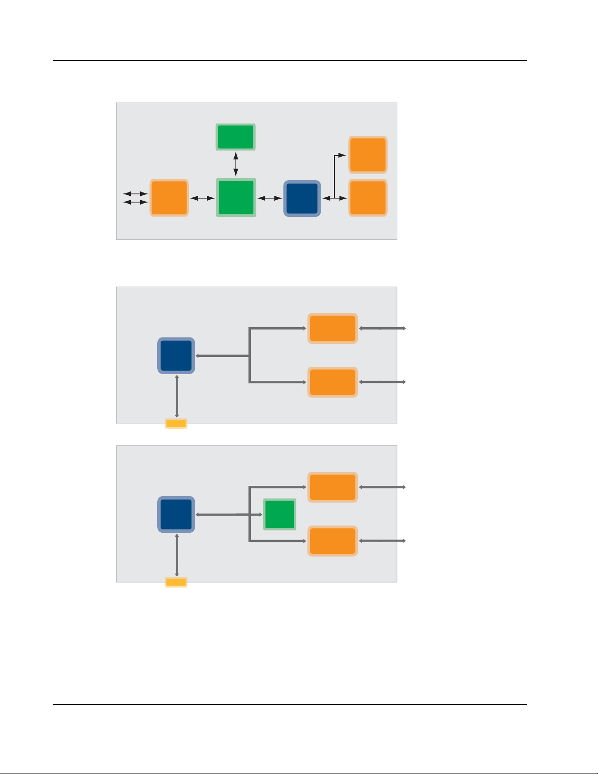
Figure 4: External Storage Application
PCI-X 133 MHz
PCI-X 133 MHz
PCIe x4
Tsi384
GbE/FC
Controller
GbE/FC
Controller
PCI 66 MHz
PCI 66 MHz
PCIe x4
Tsi384
SCSI
Controller
SCSI
Controller
IOP
DRAM
1. Functional Overview26
PCI-X
to SATA
iSCSI
GbE
with
TOE
Integrated
CPU
x4x4
Tsi384
PCI-X
to SATA
Figure 5: Server Add-in Cards for Networking and Storage
Tsi384 User Manual
May 5, 2014
Integrated Device Technology
www.idt.com
Page 27

2. Signal Descriptions
Topics discussed include the following:
• “Overview”
• “PCIe Interface Signals”
• “PCI/X Interface Signals”
• “EEPROM Interface Signals”
• “JTAG Interface Signals”
• “Power-up Signals”
• “Power Supply Signals”
2.1 Overview
27
Signals are classified according to the types defined in the following table.
Table 1: Pin Types
Pin Type Definition
3.3 OD 3.3V CMOS open-drain output
3.3 3-state 3.3V CMOS tri-state output
3.3 Bidir 3.3V CMOS bi-directional
3.3 Bidir PU 3.3V CMOS bi-directional with 265K (+/- 45K) pull-up resistor
3.3 Bidir OD 3.3V CMOS bi-directional open-drain
3.3 In 3.3V CMOS input
3.3 In PU 3.3V CMOS input with 265K (+/- 45K) pull-up resistor
3.3 Out 3.3V CMOS output
PCI/X Bidir PCI/X bi-directional
PCI/X Bidir OD PCI/X bi-directional open-drain
PCI/X In PCI/X input
PCI/X Out PCI/X output
PCI/X OD PCI/X output open-drain
Integrated Device Technology
www.idt.com
Tsi384 User Manual
May 5, 2014
Page 28

Table 1: Pin Types (Continued)
Pin Type Definition
PCIE Diff Out PCIe differential output
PCIE Diff In PCIe differential input
2.2 PCIe Interface Signals
Table 2: PCIe Interface Signals
Name Pin Type Description Design Recommendation
2. Signal Descriptions28
PCIE_PERSTn 3.3 In Master reset in:
0 = Tsi384 in reset
1 = Tsi384 in normal mode
PCIE_TXD_n[3:0]
PCIE_TXD_p[3:0]
PCIE_RXD_n[3:0]
PCIE_RXD_p[3:0]
PCIE_REFCLK_n
PCIE_REFCLK_p
PCIE_LANE_VALIDn[3
:0]
PCIE Diff Out Transmit Data. These differential pair
signals send PCIe 8b/10b encoded
symbols and an embedded clock to the
link partner.
PCIE Diff In Receive Data. These differential pair
signals receive PCIe 8b/10b encoded
symbols and an embedded clock from
the link partner.
PCIE Diff In Reference Clock. 100-MHz differential
reference clock.
3.3 out PCIe Lane Valid:
0 = Lane valid
1 = Lane invalid
Direct connect to the PERST# signal.
DC blocking capacitors must be placed
in the link between the transmitter and
the receiver. Place a 0603 or 0402
0.075uF to 0.1uF ceramic capacitor on
each TXD_n, TXD_p signal.
DC blocking capacitors must be placed
in the link between the transmitter and
the receiver; however, the DC blocking
capacitors are normally placed near the
transmitter. When designing an add-in
card, capacitors are not required on this
link. When designing a system board,
the DC blocking capacitors should be
placed near the transmitter.
Refer to the Tsi384 Board Design
Guidelines.
When connecting to LEDs, connect the
cathode on PCIE_LANE_VALIDn and
the anode to 3.3V.
Tsi384 User Manual
May 5, 2014
Integrated Device Technology
www.idt.com
Page 29

2. Signal Descriptions 29
2.3 PCI/X Interface Signals
Table 3: PCI/X Interface Signals
Name Pin Type Description Design Recommendation
PCI_ACK64n PCI/X Bidir Acknowledge 64-bit Transaction. The
bus target asserts this signal to indicate
it wants to participate in a 64-bit
transaction.
PCI_AD[63:0] PCI/X Bidir Address/Data Bus. These multiplexed
signals provide a 32/64-bit address and
64-bit data bus.
PCI_CBEn[7:0] PCI/X Bidir Command/Byte Enables. These
multiplexed signals indicate the current
transaction type.
PCI_CLK PCI/X In PCI Input Clock. This signal provides
timing for the Tsi384, either from an
external clock or from one of the
PCI_CLKO[4:0] signals (see
“Clocking”).
PCI_CLKO[4:0] PCI/X Out PCI Output Clock. PCI_CLKO[3:0] are
for driving four devices, and
PCI_CLKO[4] can feed back to
PCI_CLK to compensate for PCB track
length (see “Clocking”).
PCI_DEVSELn PCI/X Bidir Device Select. A target device asserts
this signal when it decodes its address
on the bus. The master samples the
signal at the beginning of a transaction,
and the target rescinds it at the end of
the transaction.
Pull up (8.2K) to 3.3V.
Pull up (8.2K) to 3.3V on
PCI_AD[63:32].
Pull up (8.2K) to 3.3V on
PCI_CBE[7:4].
None.
Point-to-point connection to PCI/X
device. IDT recommends a 33 Ohm
series termination resistor.
Pull up (8.2K) to 3.3V.
a
a
a
a
PCI_FRAMEn PCI/X Bidir Frame. The current initiator drives this
signal to indicate the start and duration
of a transaction, and the bus target
samples it. The bus master rescinds the
signal at the end of the transaction.
Integrated Device Technology
www.idt.com
Pull up (8.2K) to 3.3V.
Tsi384 User Manual
a
May 5, 2014
Page 30

Table 3: PCI/X Interface Signals (Continued)
Name Pin Type Description Design Recommendation
2. Signal Descriptions30
PCI_GNTn[3:0] PCI/X Bidir /
PCI/X Out
PCI_INTDn PCI/X In Interrupt D. Pull up (2.4K) to 3.3V.
PCI_INTCn PCI/X In Interrupt C. Pull up (2.4K) to 3.3V.
PCI_INTBn PCI/X In Interrupt B. Pull up (2.4K) to 3.3V.
PCI_INTAn PCI/X In Interrupt A. Pull up (2.4K) to 3.3V.
PCI_IRDYn PCI/X Bidir Initiator Ready. The bus master asserts
Bus Grant. The Tsi384 uses these
multifunction signals to grant access to
the PCI/X bus; however, they are used
differently depending on whether or not
the Tsi384 PCI/X arbiter is used. If the
arbiter is used, then PCI_GNTn[3:0] are
outputs used by the Tsi384 to grant
access to the bus (see “PCI/X
Arbitration”).
If an external arbiter is used,
PCI_GNTn[0] is an input that is driven
by the arbiter to grant the Tsi384 access
to the bus. The remaining pins,
PCI_GNTn[3:1], remain as outputs.
The input/output mode is controlled by
the PWRUP_EN_ARB pin (see
“Power-up Signals”).
this signal to indicate it is ready to
complete the current transaction.
PCI_GNTn[3:0] outputs connect directly
to the PCI device’s PCI_GNTn inputs.
Pull ups are not required on unused
outputs.
Pull up (8.2K) to 3.3V.
PCI_M66EN PCI/X In 66-MHz Enable. This signal enables the
PCI Interface for 66-MHz operation.
0 = 33-MHz operation
1 = 66-MHz operation
This signal is ignored in PCI-X mode.
PCI_M66EN must be stable and valid
around the rising edge of
PCIE_PERSTn (see “Reset”).
PCI_PAR PCI/X Bidir Parity. This signal carries even parity
across PCI_AD[31:0] and
PCI_CBEn[3:0]. The bus master
asserts this signal for the address and
write data phases. The bus target
asserts it for read data phases.
Tsi384 User Manual
May 5, 2014
Em
bedded designs
Pull down for 33 MHz and slower
operation. Pull up for greater than
33-MHz operation.
Bused designs using PCI/X slots for
add- in cards
Place a pull-up resistor (~5K to 10K) on
M66EN and route the signal from slot to
slot.
No pull-up or pull-down resistor is
required.
b
Integrated Device Technology
www.idt.com
Page 31

2. Signal Descriptions 31
Table 3: PCI/X Interface Signals (Continued)
Name Pin Type Description Design Recommendation
PCI_PAR64 PCI/X Bidir Parity for 64-bit Transaction. This signal
serves the same purpose as PCI_PAR,
but is associated with PCI_AD[63:32]
and PCI_CBEn[7:4].
PCI_PCIXCAP PCI/X In PCI-X capability. This signal determines
the PCI-X operating frequency (see
“PCI/X Clocking”).
PCI_PCIXCAP_PU PCI/X Bidir PCI-X capability pull-up (see “PCI/X
Clocking”).
PCI_PERRn PCI/X Bidir Parity Error. This signal indicates a
parity error occurred during the current
data phase. The bus target that
receives the data asserts this signal.
PCI_PMEn PCI/X In Power Management Event. This signal
indicates a power management event
occurred (see “Power Management”).
Pull-up (8.2K) to 3.3V.
Embedde
d designs
a
For PCI mode, connect to ground.
For PCI-X mode at 66 MHz, pull down
with a 10K resistor and pull up with 56K
resistor.
For PCI-X mode at 133 MHz, pull up
with 56K.
Bused designs using PCI-X slots for
add- in cards
Pull up to 3.3V with a 56K resistor and
route the signal from slot to slot.
Couple resistively to PCI_PCIXCAP
using a 1K resistor.
Pull up (8.2K) to 3.3V.
Pull up (8.2K) to 3.3V.
a
a
PCI_REQn[3:0] PCI/X In
PCI/X Bidir
Bus Request. These signals are used to
request access to the PCI/X bus. They
are used differently, however,
depending on whether or not the Tsi384
PCI/X arbiter is used. If the PCI/X
arbiter is used, then PCI_REQn[3:0] are
inputs used by external masters to
request access to the bus.
If an external arbiter is used,
PCI_REQn[0] is an output used by the
Tsi384 to request access to the bus,
while PCI_REQn[3:1] should be pulled
high, as they are still inputs.
The input/output mode is controlled by
the PWRUP_EN_ARB pin (see
“Power-up Signals”).
PCI_REQ64n PCI/X Bidir Request 64-bit Transfer. The bus
master asserts this signal to indicate it
wants to perform a 64-bit transaction.
The bus master rescinds this signal at
the end of the transaction.
Integrated Device Technology
www.idt.com
Pull up (8.2K) to 3.3V.
Pull up (8.2K) to 3.3V.
Tsi384 User Manual
a
May 5, 2014
Page 32

Table 3: PCI/X Interface Signals (Continued)
Name Pin Type Description Design Recommendation
2. Signal Descriptions32
PCI_RSTn PCI/X Out PCI/X reset: This signal resets all
devices on the PCI/X bus.
PCI_SEL100 PCI/X In Select 100-MHz frequency. This signal
selects the PCI/X operating frequency
(see Ta bl e 29 ).
PCI_SERRn PCI/X Bidir OD System Error. This signal indicates an
address or attribute phase parity error
occurred.
PCI_STOPn PCI/X Bidir Stop. A bus target asserts this signal to
indicate it wants to stop the current
transaction on the current data phase.
PCI_TRDYn PCI/X Bidir Target Ready. The bus target asserts
this signal to indicate it is ready to
complete the current data phase.
a. These pull-ups must exist somewhere on the PCI/X bus.
b. For more information on all combinations of PCI_M66EN, PCI_SEL100, and PCI_PCIXCAP, see the “Reset, Clocking, and
Initialization”.
No pull-up or pull-down resistor is
required.
Pull down for PCI 33 or 66 MHz, or
PCI-X 66 or 133 MHz.
Pull up for PCI 25 or 50 MHz, or
PCI-X 50 or 100 MHz.
Pull up (8.2K) to 3.3V.
Pull up (8.2K) to 3.3V.
Pull up (8.2K) to 3.3V.
b
a
a
a
2.4 EEPROM Interface Signals
Table 4: EEPROM Interface Signals
Name Pin Type Description Design Recommendation
SR_CLK 3.3 Out Serial ROM clock: This signal is derived
from REFCLKn/p (see “System
Diagram”).
SR_CSn 3.3 Out Serial ROM chip select: This active-low
signal activates the chip-select (CS) on
the external EEPROM.
SR_DIN 3.3 Out Serial ROM data in: This signal
transfers output data from the Tsi384 to
the EEPROM.
SR_DOUT 3.3 In PU Serial ROM data out: This signal
transfers input data from the EEPROM
to the Tsi384.
No pull-up or pull-down resistor is
required.
Tsi384 User Manual
May 5, 2014
Integrated Device Technology
www.idt.com
Page 33

2. Signal Descriptions 33
2.5 JTAG Interface Signals
Table 5: JTAG Interface Signals
Name Pin Type Description Design Recommendation
JTAG_TCK 3.3 In Test Clock. This signal clocks state
information and data into and out of the
Tsi384 during boundary scan.
JTAG_TDI 3.3 In PU Test Data Input. This signal, in
conjunction with JTAG_TCK, shifts data
and instructions into the TAP controller
in a serial bit stream.
JTAG_TDO 3.3 Out Test Data Output. This signal, in
conjunction with JTAG_TCK, shifts data
and instructions from the TAP controller
in a serial bit stream.
JTAG_TMS 3.3 In PU Test Mode Set. This signal controls the
state of the TAP controller.
JTAG_TRSTn 3.3 In PU Test Reset. This signal forces the TAP
controller into an initialized state. This
signal must be pulsed or pulled low
externally to reset the TAP controller.
TEST_BCE 3.3 In Test Boundary Scan Compatibility
Enabled. This input aids 1149.6 testing
and Scope function of PHYs.
Connect to 3.3V using a 2K pull-up
resistor.
Connect to 3.3V using a 2K pull-up
resistor.
If JTAG is not used, leave unconnected.
Connect to 3.3V using a 2K pull-up
resistor.
If JTAG is not used, connect this pin to a
2K pull-down resistor. If JTAG is used,
connect to output of AND gate where
inputs are TRST# and PERST#.
For more information, see the Tsi384
Evaluation Board User Manual.
For 1149.1 Boundary Scan testing, this
pin must be high. For 1149.6 Boundary
Scan testing, this pin must be low.
TEST_ON 3.3 In This signal controls scan shift enable. For normal operation, connect to 3.3V
using a 2K pull-up resistor.
TEST_BIDR_CTL 3.3 In PU This pin controls the direction of the
bidirectional pins as input during scan
shift.
Integrated Device Technology
For normal operation, connect to 3.3V
using a 2K pull-up resistor.
Tsi384 User Manual
www.idt.com
May 5, 2014
Page 34

2.6 Power-up Signals
Table 6: Power-up Signals
Name Pin Type Description Design Recommendation
2. Signal Descriptions34
PWRUP_CLK_MST 3.3 In PU Clock Master:
0 = Tsi384 is clock slave on the PCI/X
bus; it requires an external PCI/X bus
clock.
1 = Tsi384 is clock master on the PCI/X
bus (clock master mode); it drives the
PCI/X bus clock.
PWRUP_EN_ARB 3.3 In PU Internal PCI/X bus arbiter enable:
0 = Disable internal arbiter
1 = Enable internal arbiter
PWRUP_EXT_
CLK_SEL
PWRUP_PLL_
BYPASSn
3.3 In PU Clock select. This signal is used when
the Tsi384 is the clock master on the
PCI/X bus.
0 = Tsi384 uses the internal clock
generated from REFCLK to time the
PCI-X Interface (see “Master Mode
Clocking”).
1 = Tsi384 uses the clock on PCI_CLK
compensated through the PLL to time
the PCI-X Interface.
3.3 In PU PLL bypass. This signal bypasses the
PLL in the PCI clock generation (see
“PCI/X Clocking”).
0 = PLL bypass
1 = Normal operation
None.
None.
This signal can be set to 0 only when
the PCI bus frequency is set to 33 MHz
or less. For all other frequencies, this
signal must be set to 1.
This signal should always be tied high.
2.7 Power Supply Signals
Table 7: Power Supply Signals
Name Pin Type Description Design Recommendation
VDD Core power 1.2V core power None.
VDD_PCI I/O power 3.3 volt I/O power for PCI/X and 3.3V
I/O power for CMOS
VDD_PCIE Core power 1.2V power for SerDes Connect these signals to the 1.2V
Tsi384 User Manual
May 5, 2014
None.
source through a ferrite bead.
Integrated Device Technology
a
b
www.idt.com
Page 35

2. Signal Descriptions 35
Table 7: Power Supply Signals (Continued)
Name Pin Type Description Design Recommendation
VDDA_PCIE Analog power 3.3V analog power for SerDes Connect these signals to the 3.3V
source through a ferrite bead.
VDDA_PLL Analog power 1.2V analog power for PLL Connect these signals to the 1.2V
source through a ferrite bead.
a
b
b
VSS GND GND, core power None.
VSS_IO GND GND, I/O power None.
VSSA_PLL GND GND, analog PLL power None.
a. For filtering and decoupling information for these signals, see “Power Supply Filtering and Decoupling” in the Tsi384 Board
Design Guidelines.
b. For more information, see “Analog Power Supply Filtering” in the Tsi384 Board Design Guidelines.
Integrated Device Technology
www.idt.com
Tsi384 User Manual
May 5, 2014
Page 36

2. Signal Descriptions36
Tsi384 User Manual
May 5, 2014
Integrated Device Technology
www.idt.com
Page 37

3. Data Path
Topics discussed include the following:
• “Overview”
• “Transaction Management”
• “Buffer Structure”
• “Flow Control”
• “Prefetching Algorithm”
• “Short Term Caching”
• “Lane Reversal and Polarity Reversal”
3.1 Overview
37
The Tsi384 uses two buffering methods for transferring data between its PCIe and PCI/X ports:
• Two-stage buffering for its upstream data path
• One-stage buffering in its downstream data path
These buffering methods are summarized in the following sub-sections.
3.1.1 Upstream Data Path
Two-stage buffering in the upstream path consists of two different sized buffers for each transaction
type: posted, non-posted, and completion (see Figure 6).
The first-stage buffering in the PCI Core, which supports the store and forward method, meets the
synchronization requirements of PCI and PCIe. This buffer design also provides optimized throughput
and improved latencies.
The second-stage buffering in the PCIe Core, which supports the cut-through method, handles the
possible backpressure due to scaled down link, lack of flow control credits, and replay. Posted and
completion buffers allow the Tsi384 to accept a few more cycles of data transfer even after the
assertion of stall which indicates to the initiator in the PCI Core to stop the data transfer. This buffer
design ensures idle cycles are not inserted in data cycles while forwarding TLPs to its egress block.
Integrated Device Technology
www.idt.com
Tsi384 User Manual
May 5, 2014
Page 38

Figure 6: Upstream Data Path
S
c
r
a
m
b
l
e
r
r
Pos ted FIFO
(512 bytes)
Non Posted FIFO
4 Entrie s
Co mpl et i o n F IFO
(64 by tes )
Retry Buffer (2 KB)
Erro r Message TL P
EHU
CSR
PME_ n
M
a
s
te
r
In
t
e
r
fa
c
e
T
a
r
g
e
t
In
t
e
r
fa
c
e
Posted Bu ffer (4 KB)
Non Po sted Q ueue
8 En tri es
Dow ns t rea m Read
Co mp le tion Buffer
(512 bytes)
PM C
PM E
Mesaage
TLP
Pos ted R equest
No n-Po s ted
Request
Co mp leti o ns
Cl ai m
Cyc le
Add res s
De co de r
2ndS tag e Buf fer ing
C u t th ro ug h
1stS tag e Buf fering
S tor e an d For w ar d
PCIe C ore
PCI/X Core
Spli t
Co m pl e tion
Devi ce C o re
Inte rfa ce
3. Data Path38
3.1.2 Downstream Data Path
In the downstream path, the T si384 uses one-stage buffering for each type of transaction (see Figure 7).
These buffers support the store and forward method, receive flow control, protocol differences,
synchronization, and error handling requirements.
Tsi384 User Manual
May 5, 2014
Integrated Device Technology
www.idt.com
Page 39

3. Data Path 39
P
C
I
-
X
I
n
t
e
r
f
a
c
e
R
x
S
E
R
D
E
S
D
e
-
s
c
r
a
m
b
l
e
r
B
y
t
e
U
n
-
s
tr
i
p
e
r
LCRC
Che cke r
Pa ck et
Dec od er
Ad dress
Decoder
ECR C
Che cke r
TLP
Erro r
Detec ter
Req ues t
Generato r
A
r
b
i
t
e
r
M
a
s
t
e
r
I
n
t
e
r
f
a
c
e
T
a
r
g
e
t
I
n
t
e
r
f
a
c
e
Po sted Buffer
(5 12 Bytes)
No n-Posted Queue
4 Entries
Up st ream Re ad
Completion Buffer
(4 K B)
PCIe C ore
PCI Core
Receive Flow
Control Buffers
D e laye d C om ple t ion
Device Core Interface
Split Co mp letion
Figure 7: Downstream Data Path
3.2 Transaction Management
The following sub-sections describe how the Tsi384 handles upstream and downstream transactions.
3.2.1 Upstream Transaction Management
Transactions that originate on the PCI/X Interface that are destined for the PCIe Interface are stored in
the respective queues or buffers in the PCI/X cloc k domain, and are then forwarded to the PCIe Core
(see Figure 6). PCI/X buffer logic decomposes the received transactions as per the PCIe constraints
(for example, MAX_RD_SIZE, MAX_PAY_SIZE, RCB, and 4-KB address boundary). Three sets of
data and control signals for the three types of transactions (posted, non-posted, and completions) are
used between the PCI/X and PCIe Cores.
Transactions are stored temporarily in the PCIe Core buffers before they are used to construct TLPs,
and are then made visible to TLP arbiter. The TLPs are processed by the TLP arbiter only after
message, posted, completion, and non-posted TLPs) in a round-robin mode if sufficient credits and
ordering rules are satisfied. The TLP arbiter selects one of the five input TLPs (error message, PME
retry buffer space is available for the specific TLPs. The TLP arbiter continues to check the available
credit and retry buffer space against each of the active inputs, and selects the one that meets the
constraint. The ECRC adder calculates and appends a 32-bit ECRC value to the end of the TLP
selected by the arbiter if ECRC generation is enabled by software, and then forwards the TLP to the
Data link layer.
Integrated Device Technology
www.idt.com
Tsi384 User Manual
May 5, 2014
Page 40

The Data link layer applies a sequence number to the TLP received from transaction layer block, and
then calculates and appends a 32-bit LCRC value to ensure integrity during the transmission across the
physical lanes. A copy of the TLP sent to the physical layer is stored in the retry buffer for future replay
if there is negative acknowledgment from the other end component. The Retry buffer replays the stored
unacknowledged TLPs if it receives a NAK or replay timer expiration.
The Byte striper block of the physical layer unit appends start and end characters to the TLP received
from Data link layer, and then multiplexes the bytes of the packet onto the lanes. These bytes on the
lanes are scrambled using LFSR to eliminate repetitive bit patterns in the bit stream. The scrambled
8-bit characters are sent to the SerDes to convert to a 10-bit character in order to transmit it in a serial
bit stream on the physical lanes.
3.2.2 Downstream Transaction Management
In the downstream path, the physical layer unit converts the incoming serial bit stream into a parallel
symbol stream, de-scrambles the bytes in the transmit path, assembles packets, and then sends them to
the Data link layer unit (see Figure 7).
The Data link layer unit checks for LCRC and sequence number errors for packets received from the
physical layer unit. If there are no errors, LCRC and sequence number fields are stripped and resultant
TLP is sent to Transaction layer unit.
3. Data Path40
The Transaction layer unit checks for ECRC errors and framing violations based on header fields and
ECRC fields in the TLP received from the Data link layer unit. It extracts routing information based on
the header fields and determines whether to forward or reject the TLP. The ECRC field is stripped and
the resulting information in the TLP header, payload, and any detected error information, is sent to the
PCI Core.
The T s i384 uses receive flow control buffers in the PCI Core instead of in the PCIe Core to store
downstream requests or completions to be forwarded on the PCI/X Interface.
3.3 Buffer Structure
The following sub-sections describe the three Tsi384 buffer structures:
• Upstream non-posted buffer
• Upstream posted buffer
• Downstream non-posted buffer
• Downstream posted buffer
3.3.1 Upstream Non-posted Buffer
The 4-KB, non-posted data buffer stores the data returned from the root complex for memory or I/O
read transactions that are initiated by PCI/X devices. This buffer contains eight independent 512-byte
buffers to allow for multi-threading.
Tsi384 User Manual
May 5, 2014
Integrated Device Technology
www.idt.com
Page 41

3. Data Path 41
Every 512-byte buffer also consists of 32-byte sub-sections in PCI mode and 128-byte subsections in
PCI-X mode. In PCI mode, the T si384 allows the delayed response data transfer to the requester only if
the programmed number of 32-byte chunks of data are accumulated in the data buffer (see
CPL_INIT_COUNT in “PCI Miscellaneous Control and Status Register”). In PCI-X mode, the Tsi384
initiates split completion transactions only on 128-byte boundaries. However, read completions with
byte counts larger than 128 bytes can be returned to the PCI-X bus provided the data is available in the
buffer.
The T si384 continues to try the outstanding split completion transactions in a round-robin fashion, even
if the current split transaction received a retry or abort response.
While each request queue entry has up to 512 bytes of buffer space, in order to keep data flowing
efficiently, the 128-byte sub-sections are reused as needed when they are emptied. This means that
when the PCIe and PCI/X Interfaces are operating at similar frequencies and there is little bus
contention, long transfers can proceed without disconnection after the initial latency needed to fill the
first 128-byte sub-section. For large transfers when the PCI/X bus is operating at low frequency,
disconnections can occur on every 128 bytes as the 512-byte buffer becomes empty.
This buffer contains an eight-deep request queue that stores ad dress and command information for PCI
delayed transactions (reads/writes) and PCI-X split transactions (reads/writes). This handles
non-posted transactions that originate on the PCI/X Interface and are destined to devices on the PCIe
Interface.
3.3.1.1 Non-posted Write Buffer
The Tsi384 supports one non-posted write transaction. Similar to read requests, its request information
is stored in one of the eight request queue entries, and its data is stored in a 32-bit register. Non-posted
write requests are forwarded onto the PCIe Core in two PCIe clock cycles. Request information is
forwarded in the first cycle, while 32-bit data is forwarded in the second cycle.
3.3.2 Upstream Posted Buffer
The upstream posted buffer is a FIFO of size 4-KB that stores memory write transactions that originate
on the PCI/X Interface and are destined to devices on PCIe Interface. The Tsi384 completes the posted
transactions on the originating bus before forwarding them to the PCIe Interface. Unlike the read
buffers, the amount of space assigned to each transaction is dynamic. A single transaction can use
4-KB of buffer space. The Tsi384 translates all types of memory write transactions from the PCI/X
Interface to memory write requests on the PCIe Interface. The Tsi384 terminates a new transaction with
retry and an active transaction with disconnect if sufficient buffer space is not available.
The Tsi384 uses an 8-deep request FIFO to store the request information, including first and last
Dwords byte enables of the received transactions.
Memory write transactions can contain any or al l in valid payload bytes, where as memory write and
invalidate (MWI) or memory write block command transactions carry all the valid payload bytes. The
Tsi384 decomposes the received transactions with non-contiguous byte enables on 32-byte boundaries
while writing into the request FIFO.
The PCI Core makes a request to the PCIe Core if one of the following conditions is met:
• All data bytes of the transaction are received and are stored in the data buffer
Integrated Device Technology
www.idt.com
Tsi384 User Manual
May 5, 2014
Page 42

• Received data bytes count exceeds the programmed threshold value (see UPST_PWR_THRES in
“Upstream Posted Writ e Threshold Register”)
• Received data bytes count exceeds the PCIe maximum payload size (see MAX_PAY_SIZE in
“PCIe Device Control and Status Register”)
• Address plus received data bytes count exceeds 4 KB
• Data with non-contiguous byte enables
3.3.3 Downstream Non-posted Buffer
The 512-byte, downstream non-posted buffer stores the data returned for the non-posted requests that
originate on the PCIe Interface and are destined for PCI/X devices.
This buffer is divided into four independent 128-byte buffers to allow for multi-threading. Each
128-byte buffer has a read queue that provides up to four active non-posted requests. The Tsi384
decomposes the read request while placing it on the PCI/X Interface if the requested read data size
exceeds the maximum buffer size of 128 bytes. This means a downstream read request of 512 bytes
would be divided into four, 128-byte read completions.
The Tsi384 continues to process outstan ding non-posted transactions in a round-robin fashion. An
active, non-posted transaction is either retried or aborted.
3. Data Path42
3.3.4 Downstream Posted Buffer
The 512-byte downstream posted write buffer stores the payload of memory write transactions that
originate on the PCIe Interface and are destined for PCI/X devices. The amount of space assigned to
each transaction is dynamic. A single transaction can use 512 bytes of buffer space.
The Tsi384 uses an 8-deep request FIFO to store the request information, including the first and last
Dwords byte enables. The Tsi384 initiates a transaction on the PCI/X Interface only after a complete
packet is stored in the buffer. The Tsi384 attempts another outstanding transaction only if the current
transaction is either successfully completed or terminated with either master or target abort.
3.4 Flow Control
The Tsi384 handles packet-based protoco l on its PCIe Interface, and transaction-based protocol on its
PCI/X Interface. PCI/X requesters initiate transactions without prior knowledge on receiver buffer
status. As a result, flow control is managed through retries and disconnects that can waste bus
bandwidth. In comparison, PCIe requesters initiate requests while having prior knowledge on receiver
buffer availability status, and therefore, eliminate the wasteful effects of unnecessary retries and
disconnects.
The T s i384 does not issue retries or disconnects on the PCI/X Interface for completions returned for a
downstream read request, but may issue retries or disconnects for a posted or non-posted transaction on
the PCI/X Interface based on the buffer space availability.
Tsi384 User Manual
May 5, 2014
Integrated Device Technology
www.idt.com
Page 43

3. Data Path 43
The Tsi384 uses flow control buffers in the PCI Core for three categories of downstream traffic. The
amount of flow control buffer space availability is conveyed to the other end of the component using
flow control credits. The Tsi384 advertises infinite credits for completions as it ensures enough buffer
space is available to store the returned completion data before initiating a read request. The Tsi384
advertises initial flow control credits as follows. Each credit of data is 16 bytes.
Table 8: Initial Credit Advertisement
Credit Type Initial Advertisement
Posted Header (PH) 0x08
Posted Data (PD) 0x020
Non-Posted Header (NPH) 0x04
Non-Posted Data (NPD) 0x01
Completion Header (CPLH) 0x00 (Infinite)
Completion Data (CPLD) 0x000 (Infinite)
3.5 Prefetching Algorithm
To optimize data throughput, the Tsi384 prefetches read data from a target device when the
PCI/X Interface is configured in PCI mode. The Tsi384 does not prefetch additional read data when
operating in PCI-X mode because the amount of data requested is specified in the byte count. The
T si384 prefetches the data by default for the transact ion that uses Memory Read Line or Memory Read
Multiple command. The Tsi384 does not prefetch the data by default for the transaction that uses the
memory read command since the bridge does not know whether or not the transaction address falls in
prefetchable region.
The prefetch algorithm is configured for various commands as follows:
• Memory read – Controlled by P_MR, MRL_66 and MRL_33 of the “Prefetch Control Register”.
The default value of these bits indicates that either one Dword in 32-bit bus mode or two Dwords
in 64-bit bus mode is prefetched.
• Memory read line – Controlled by P_MRL, MRL_66 and MRL_33 of the “Prefetch Control
Register”. The default value of these bits indicates that either 128 bytes in 32-bit bus mode or
256 bytes in 64-bit bus mode is prefetched. The Tsi384 prefetches one cacheline if P_MRL is set to
0.
• Prefetch algorithm for memory read mult ipl e command is controlled by P_MRM, MRM_66 and
MRM_33 of the “Prefetch Control Register”. The default value of these bits indicates that either
256 bytes in 32-bit bus mode or 384 bytes in 64-bit bus mode is prefetched. The T si384 prefetches
two cachelines if P_MRM is set to 0.
Integrated Device Technology
www.idt.com
Tsi384 User Manual
May 5, 2014
Page 44

3.6 Short Term Caching
This feature provides performance improvements in situations where upstream devices are not able to
stream data continuously to meet the prefetching needs of the Tsi384. As defined in the PCI-to-PCI
Bridge Specification (Revision 1.2), when the bus master completes a transaction, the bridge is required
to discard the balance of any data that was prefetched for the master. To prevent performance im pa cts
when dealing with devices between requester and completer that can only stream data of 128 to 512
bytes due to buffering constraints, the Tsi384 uses “Short Term Caching.” This feature applies only
when the PCI/X Interface is operating in PCI mode, and provides a time-limited read data cache in
which the T si384 will not discard prefetched read data after the request completes on the initiating bus.
To enable Short Term Caching, set the STC_EN bit in the “PCI Miscellaneous Control and Status
Register”. When enabled, the Tsi384 does not discard the additional prefetched data when the read
transaction completes on the initiating bus. The Tsi384 then continues to prefetch data up to the amount
specified in the “Prefetch Control Register”. If the initiator generates a new transaction that requests
the previously prefetched data, the Tsi384 returns that data.
The Tsi384 discards data after some of the data for a request is returned to the initiator and one of the
following conditions is met:
• Short-term discard timer is expired before the initiator has requested additional data (see
“Short-term Caching Period Register”).
3. Data Path44
• An upstream posted transaction is received on the PCI/X Interface
Short-term caching should only be used in systems that can ensure the data provided to the
master has not been modified since the initial transaction.
3.7 Lane Reversal and Polarity Reversal
The Tsi384 supports lane reversal, lane degradation, and polarity reversal. For information on how to
use these features, see the Tsi384 Board Design Guidelines.
Tsi384 User Manual
May 5, 2014
Integrated Device Technology
www.idt.com
Page 45

4. Addressing
Topics discussed include the following:
• “Overview”
• “Memory-mapped I/O Space”
• “Prefetchable Space”
• “I/O Space”
• “VGA Addressing”
• “ISA Addressi ng”
• “Non-transpar ent Addressing”
• “Opaque Addressing”
45
4.1 Overview
This chapter discusses the various types of address decoding performed by the Tsi384 when it forwards
transactions upstream and downstream. The memory and I/O address ranges are defined using a set of
base and limit registers in the bridge’s configuration header. The base and limit address registers define
the address ranges that a bridge forwards downstream transactions. These registers are effectively
inversely decoded to determine the address ranges on the PCI/X Interface for transactions that are
forwarded upstream to the PCIe Interface.
4.2 Memory-mapped I/O Space
Memory transactions are forwarded across the T si384 when their address falls within a window defined
by one of the following registers:
• “PCI Memory Base and Limit Register”
• “PCI PFM Base and Limit Register”
The memory-mapped I/O address spacing maps memory address ranges of devices that are not
prefetchable. For PCI to PCIe reads, prefetching occurs in this space only if the Memory Read Line or
Memory Read Multiple commands are issued on the PCI bus. When either of these commands is use d,
the quantity of data prefetched is determined by the prefetching algorithm defined in “Prefetching
Algorithm”. For PCI-X to PCIe reads, the number of bytes to read is determined by the transaction size
requested in the PCI-X attributes. For PCIe-to-PCI or PCI-X reads, the number of bytes to read is
determined by the Memory Read Request TLP.
Integrated Device Technology
www.idt.com
Tsi384 User Manual
May 5, 2014
Page 46

4. Addressing46
Memory Base
Memory Limit
Downstream
Upstream
Memory Base
Memory Limit
Downstream
Upstream
The response of the bridge to memory-mapped I/O transactions is controlled by the following:
•MS bit in “PCI Control and Status Register” – This bit must be set to allow memory transactions to
be forwarded downstream. If not set, all memory transactions on the PCI/X bus are forwarded to
the PCIe link. In addition, if not set, all memory requests on the PCIe Interface are completed with
an Unsupported Request status.
• BM bit in “PCI Control and Status Register” – This bit must be set to allow memory transactions to
be forwarded upstream. If this bit is not set, all memory transactions on the PCI/X bus are ignored.
• VGA_EN bit in “PCI Bridge Control and Interrupt Register”
The T si384 forwards memory transact ions downstream from its PCIe I nterface to its PCI/X Interface if
a memory address is in the range defined by the Memory Base and Memory Limit registers (when the
base is less than or equal to the limit), as shown in Figure 8. A memory transaction on the PCI/X
Interface that is within this address range, however, is not be forwarded upstream to the PCIe Interface.
Any memory transactions on the PCI/X Interface that are outside this address range are forwarded
upstream to the PCIe Interface (provided they are not in the address range defined by the set of
prefetchable memory address registers).
Figure 8: Memory-mapped I/O Address Space
Tsi384 User Manual
May 5, 2014
Integrated Device Technology
www.idt.com
Page 47

4. Addressing 47
The memory-mapped I/O address range that is defined by the Base and Limit registers are always
aligned to a 1-MB boundary and has a size granularity of 1 MB.
4.3 Prefetchable Space
The prefetchable address space maps memory address ranges of devices that are prefetchable; that is,
devices that do not have side-effects during reads. For PCI-to-PCIe reads, prefetching occurs in this
space for all memory read commands (MemRd, MemRdLine, MemRdMult) issued on the PCI bus. For
these Read commands, the Tsi384 prefetches data according to prefetching algorithm defined in
“Prefetching Algorithm”. For PCIe-to-PCI/X reads, the number of bytes to be read is determined by the
Memory Read Request.
The Prefetchable Memory Base, Prefetchable Memory Limit, Prefetchable Base Upper 32 Bits, and
Prefetchable Limit Upper 32 Bits registers in the bridge configuration header specify an address range
that is used by the bridge to determine whether to forward PCIe and PCI/X memory read and memory
write transactions across the bridge. The prefetchable memory address range defined by these registers
is always aligned to a 1-MB boundary and has a size granularity of 1 MB. If the address specified by
the Prefetchable Memory Base and Prefetchable Base Upper 32 Bits registers is set to a value higher
than the address specified by the Prefetchable Memory Limit and Prefetchable Limit Upper 32 Bits
registers, the address range is disabled.
Following register bits effect the response by the bridge to memory transactions:
• Memory Enable bit in “PCI Control and Status Register”
• Bus Master Enable bit in “PCI Control and Status Register”
• VGA Enable bit in “PCI Bridge Control and Interrupt Register”
The T si384 forwards memory trans actions downstream from its PCIe Interface to its PCI/X Interface if
a memory address is in the range defined by the Prefetchable Memory Base and Prefetchable Memory
Limit registers. Conversely, a memory transaction on the PCI/X Interface that is within this address
range is not be forwarded upstream to the PCIe Interface. Any memory transactions on the PCI/X
Interface that are outside this address range are forwarded upstream to the PCIe Interface (provided
they are not in the address range defined by the memory-mapped I/O address range registers).
If the Prefetchable Memory Base is programmed to have a value greater than the Prefetchable Memory
Limit, then the prefetchable memory range is disabled. In this case, all memory transaction forwarding
is determined by the memory-mapped I/O base and limit registers. Note that all four prefetchable base
and limit registers must be considered when disabling the prefetchable range.
Unlike non-prefetchable memory-mapped I/O memory, Prefetchable memory can be located below,
above, or span across the first 4-GB address boundary. Figure 9 illustrates a prefetchable memory
window that spans across the 4-GB address boundary. Memory locations above 4 GB are accessed
using 64-bit addressing. PCIe memory transactions that use the Short Address (32-bit) format can
target a non-prefetchable memory window or the portion of a prefetchable memory window that is
below the first 4-GB address boundary. Memory transactions that use the Long Address (64-bit) format
can target the portion of a prefetchable memory window that is at or above the first 4-GB address
boundary.
Integrated Device Technology
www.idt.com
Tsi384 User Manual
May 5, 2014
Page 48

Figure 9: 64-bit Prefetchable Memory Address Range
Downstream
Upstream
Memory Mapped I/O
Secondary Interface
Prefetchable Memory
Downstream
Upstream
Memory Mapped I/O
Secondary Interface
Prefetchable Memory
4. Addressing48
4.4 I/O Space
I/O Base, I/O Limit, I/O Base Upper 16 Bits, and I/O Limit Upper 16 Bits registers in the Tsi384
configuration header specify an address range that is used by the br idge to de termine whether to
forward I/O read and I/O write transactions across the bridge. If the address specified by the I/O Base
and I/O Base Upper 16 Bits registers is set to a value greater than the address specified by the I/O Limit
and I/O Limit Upper 16 Bits registers, the address range is disabled.
The response of the bridge to I/O transactions is controlled by the following configuration register bits:
• I/O Space Enable bit in “PCI Control and Status Register”
• Bus Master Enable bit in “PCI Control and Status Register”
• ISA Enable bit in “PCI Bridge Control and Interrupt Register”
• VGA Enable bit in “PCI Bridge Control and Interrupt Register”
The I/O Enable bit must be set for any I/O transaction to be forwarded downstream. If this bit is not set,
all I/O transactions on the PCI/X bus are forwarded to the PCIe link. If this bit is not set, all PCIe
Interface I/O requests are completed with Unsupported Request status.
Tsi384 User Manual
May 5, 2014
Integrated Device Technology
www.idt.com
Page 49

4. Addressing 49
Secondary Interface
0x0_C000 – 0x0_FFFF
0x0_B000 – 0x0_BFFF
0x0_A000 – 0x0_AFFF
0x0_9000 – 0x0_9FFF
0x0_8000 – 0x0_8FFF
0x0_0000 – 0x0_7FFF
Downstream
Upstream
Secondary Interface
0x0_C000 – 0x0_FFFF
0x0_B000 – 0x0_BFFF
0x0_A000 – 0x0_AFFF
0x0_9000 – 0x0_9FFF
0x0_8000 – 0x0_8FFF
0x0_0000 – 0x0_7FFF
Downstream
Upstream
The Bus Master Enable bit must be set for any I/O transaction to be forwarded upstream. If this bi t is
not set, all I/O transactions on the PCI/X bus are ignored.
If ISA Enable bit is set, the bridge does not forward any I/O transactions downstream that are in the top
768 bytes of each 1-KB block within the first 64 KB of address space. Only transactions in the bottom
256 bytes of each 1-KB block are forwarded downstream. If the ISA Enable bit is clear, then all
addresses within the range defined by the I/O base and limit registers are forwarded downstream. I/O
transactions with addresses above 64 KB are forwarded according to the range defined by th e I/O base
and limit registers. If the ISA Enable bit is set, the bridge forwards upstream any I/O transactions on
the PCI/X bus that are in the top 768 bytes of each 1-KB block within the first 64 KB of address space,
even if the address is within the I/O base and limit. All other transactions on the PCI/X bus are
forwarded upstream if they fall outside the range defined by the I/O base and limit registers. If the ISA
Enable bit is clear, then all PCI/X bus I/O addresses outside the range defined by the I/O base and limit
registers are forwarded upstream.
Figure 10: I/O Address Space
Integrated Device Technology
www.idt.com
Tsi384 User Manual
May 5, 2014
Page 50

A bridge uses the I/O Base and I/O Limit registers to determine whether to forward I/O transactions
across the bridge, as shown in Figure 10. The I/O address range defined by these registers is always
aligned to a 4-KB boundary and has a size granularity of 4 KB. A bridge forwards I/O read and I/O
write transactions from its PCIe Interface to its PCI/X Interface if the address is in the range defined by
the I/O base and I/O limit registers (when th e base is less than or equal to the limit). Conversely, I/O
transactions on the PCI/X bus in the address range defined by these registers are not forwarded
upstream by the bridge. I/O transactions on the PCI/X bus that are outside the defined address range are
forwarded upstream.
4.5 VGA Addressing
The Tsi384 supports VGA addressing. The VGA_EN bit in the “PCI Bridge Control and Interrupt
Register” controls the response by the bridge to both VGA frame buffer addresses and to VGA register
addresses. If the VGA Enable bit is set, the bridge decodes and forwards memory accesses to VGA
frame buffer addresses and I/O accesses to VGA registers from the PCIe Interface to the PCI/X
Interface (and block forwarding from PCI/X to PCIe of these same accesses).
The VGA_16BIT_EN bit in the “PCI Bridge Control and Interrupt Reg ister” selects between 10-bit
and 16-bit VGA I/O address decoding, and is applicable when the VGA Enable bit is 1.
4. Addressing50
VGA memory addresses are 0x0A_0000 through 0x0B_FFFF
VGA I/O Addresses (Address bits 15:10 are not decoded when the VGA 16-Bit Decode bit is 0b) are:
• Address bits 9:0 = 0x3B0 through 0x3BB and 0x3C0 through 0x3DF (VGA 16-Bit Decode bit is
0b)
• Address bits 15:0 = 0x03B0 through 0x03BB and 0x03C0 through 0x03DF (VGA 16-bit Decode
bit is 1b)
The VGA Palette Snoop Enable bit is implemented as read-only with a value of zero.
4.6 ISA Addressing
The Tsi384 supports ISA addressing through ISA Enable bit in the “PCI Bridge Control and Interrupt
Register”. The ISA Enable affects only I/O addresses that are in the bridge’s I/O range (as defined by
the I/O Base, I/O Base Upper 16 Bits, I/O Limit, and I/O Limit Upper 16 Bits) and in the first 64 KB of
PCI/X I/O Space (0000 0000h to 0000 FFFFh). If this bit is set and the I/O address meets the stated
constraints, the T si384 blocks the forwarding of I/O transactions downstream if the I/O address is in the
top 768 bytes of each naturally aligned 1-KB block. If the ISA Enable bit is clear, the Tsi384 forwards
downstream all I/O addresses in the address range defined by the I/O Base and I/O Limit registers.
If the ISA Enable bit is set, I/O transactions on the PCI/X bus in the top 768 bytes of any 1-KB address
block within the first 64 KB of PCI/X I/O space is forwarded upstream, even if the address is between
the I/O base and I/O limit addresses. Figure 11 illustrates this mapping for a 4-KB range.
The ISA Enable bit only affects the I/O address decoding behavior of the bridge. It does not affect the
bridge's prefetching, posting, ordering, or error handling behavior.
Tsi384 User Manual
May 5, 2014
Integrated Device Technology
www.idt.com
Page 51

4. Addressing 51
Secondary Interface
0x0_xD000 – 0x0_xFFF
0x0_xC00 – 0x0_xCFF
0x0_x000 – 0x0_x0FF
0x0_x400 – 0x0_x4FF
0x0_x800 – 0x0_x8FF
Downstream
Upstream
0x0_x900 – 0x0_x9FF
0x0_x500 – 0x0_x7FF
0x0_x100 – 0x0_x3FF
Secondary Interface
0x0_xD000 – 0x0_xFFF
0x0_xC00 – 0x0_xCFF
0x0_x000 – 0x0_x0FF
0x0_x400 – 0x0_x4FF
0x0_x800 – 0x0_x8FF
Downstream
Upstream
0x0_x900 – 0x0_x9FF
0x0_x500 – 0x0_x7FF
0x0_x100 – 0x0_x3FF
Figure 11: ISA Mode I/O Addressing
4.7 Non-transparent Addressing
At power-up, the host processor discovers the need for non-transparent bridging and enables the
address remapping of prefetchable, non-prefetchable, and I/O ranges through configuration. Before
enabling address remapping of the base and limit values, the remapped address ranges need to be
programmed. The “Downstream Non-transparent Address Remapping Registers” allow downstream
accesses to be mapped to arbitrary positions in PCI/X memory space. While the Memory Base and
Limit registers always define the range of addresses to be claimed on the PCIe link and forwarded to
the PCI/X bus, cycles that are claimed have their addresses modified because of the difference in the
base addresses of the windows on the two buses.
Integrated Device Technology
www.idt.com
Tsi384 User Manual
May 5, 2014
Page 52

4.7.1 PCIe to PCI/X Non-prefetchable Address Remapping
Downstream transactions that fall within the address window defined by the “PCI Memory Base and
Limit Register” are remapped according to the address window defined by the “Secondary Bus
Non-prefetchable Address Remap Control Register” and “Secondary Bus Non-prefetchable Upper
Base Address Remap Register”. The following equations describe the address remapping process:
• PriSecNPDiff = PriNPBase - SecNPBase, where
— PriSecNPDiff: Defines the difference between the Primary Non-prefetchable Base and the
Secondary Non-prefetchable Base.
— PriNPBase: Defined in the previous paragraph.
— SecNPBase: Defined by “Secondary Bus Non-prefetchable Address Remap Control Register”
and “Secondary Bus Non-prefetchable Upper Base Address Remap Register”.
• SecNPAddr = PriNPAddr - PriSecNPDiff, where
— SecNPAddr: Defines the remapped address that the Tsi384 presents on the PCI/X bus.
— PriNPAddr: Defines the address presented to the Tsi384 that falls within the registers
described in the previous paragraph.
— PriSecNPDiff: See previous bullet.
4. Addressing52
4.7.2 PCIe to PCI/X Prefetchable Address Remapping
Downstream transactions that fall within the address window defined by the “PCI PFM Base and Limit
Register”, “PCI PFM Base Upper 32 Address Register”, and “PCI PFM Limit Upper 32 Address
Register”are remapped according to the address window defined by the “Secondary Bus Prefetchable
Address Remap Control Register” and “Secondary Bus Prefetchable Upper Base Address Remap
Register”. The following equations describe the address remapping process:
• PriSecPFDiff = PriPFBase - SecPFBase, where
— PriSecPFDiff: Defines the difference between the Primary Prefetchable Base and the
Secondary Prefetchable Base.
— PriPFBase: Defined by the registers listed above.
— SecPFBase: Defined by “Secondary Bus Prefetchable Address Remap Control Register” and
“Secondary Bus Prefetchable Upper Base Address Remap Register”.
• SecPFAddr = PriPFAddr - PriSecPFDiff, where
— SecPFAddr: Defines the remapped address the Tsi384 presents on PCI/X bus.
— PriPFAddr: Defines the address presented to the Tsi384 that falls within the registers
described in the previous paragraph.
— PriSecPFDiff: See previous bullet.
Tsi384 User Manual
May 5, 2014
Integrated Device Technology
www.idt.com
Page 53

4. Addressing 53
4.7.3 PCI/X to PCIe Address Remapping
Because the addresses of the downstream memory windows on the PCI/X bus have been shifted from
their locations on the PCIe link, the address range of cycles that a bridge will not claim on the PCI/X
bus must also be shifted. Therefore, memory cycles with addresses from SecNPBase (see “Secondary
Bus Non-prefetchable Address Remap Control Register” and “Secondary Bus Non-prefetchable Upper
Base Address Remap Register”) to SecNPLimit or from SecFPBase (see “Secondary Bus Prefetchable
Address Remap Control Register” and “Secondary Bus Prefetchable Upper Base Address Remap
Register”) to SecFPLimit will not be claimed by the bridge on the PCI/X bus.
The Secondary Bus Non-prefetchable Limit is described in the following equation:
• SecNPLimit = PriNPLimit - PriSecNPDiff, where
— PriNPLimit: Defined by “PCI Memory Base and Limit Register” and the additional “Primary
Bus Non-prefetchable Upper Limit Remap Register”.
— PriSecNPDiff: Defines the difference between the Primary Non-prefetchable Base and the
Secondary Non-prefetchable Base.
The Secondary Prefetchable Limit is described in the following equation:
• SecPFLimit = PriPFLimit - PriSecPFDiff, where
— PriPFLimit: Defined by “PCI PFM Base and Limit Register” and “PCI PFM Base Upper 32
Address Register”.
— PriSecPFDiff: Defines the difference between the Primary Prefetchable Base and the
Secondary Prefetchable Base.
Once the address is claimed as defined above, a memory cycle is forwarded from the PCI/X bus to the
PCIe link with its address modified according to the Non-transparent Address (NTMA) remapping
windows (see offsets 0x68 to 0x7C):
• NTMA window remapping
The NTMA Secondary Base (see “NTMA Secondary Lower Base Register” and “NTMA Secondary
Upper Base Register”) and NTMA Secondary Limit (see “NTMA Secondary Lower Limit Register”
and “NTMA Secondary Upper Limit Register”) define memory windows in the PCI/X bus memory
space that are mapped to arbitrary positions on the PCIe link. The resulting location of the NTMA
window on the PCIe link is defined by the following equations:
• PriSecNTMADiff = PriNTMABase - SecNTMABase, where
— PriNTMABase: Defined by “NTMA Control Register” and “NTMA Primary Upper Base
Register”.
— SecNTMABase: Defined by “NTMA Secondary Lower Base Register”
and “NTMA
Secondary Upper Base Register”.
• PriNTMALimit = SecNTMALimit + PriSecNTMADiff, where
— SecNTMALimit: Defined by “NTMA Secondary Lower Limit Register” and “NTMA
Secondary Upper Limit Register”.
— PriSecNTMADiff: See previous bullet.
Integrated Device Technology
www.idt.com
Tsi384 User Manual
May 5, 2014
Page 54

4. Addressing54
NTMA Window
Prefetchable Window
Non-prefetchable Window
NTMA Window
Prefetchable Window
Non-prefetchable Window
PCIe Address Space PCI Address Space
8000_0000
BFFF_FFFF
3FFF_FFFF
0000_0000
9_C00_0000
A_FFFF_FFFF
C000_0000
1_FFFF_FFFF
C_C000_0000
C_FFFF_FFFF
4000_0000
7FFF_FFFF
A memory cycle whose address falls within a NTMA window on the PCI/X bus will have its address
on the PCIe link modified by the following equation:
• PriNTMAAddr = SecNTMAAddr + PriSecNTMADiff, where
— SecNTMAAddr: Secondary NTMA Address, which must fall within the window defined by
the NTMA Secondary Base and Limit registers.
— PriSecNTMADiff: See previous bullet.
Transactions that are claimed on PCI/X Interface, and which are outside the NTMA window, are
forwarded upstream without address remapping. Software should ensure that the location of the NTMA
window on the PCI/X bus is outside of the PCI/X bus memory windows, and that the NTMA window
on the PCIe link is outside of the PCIe link memory windows, or un defined operation may result.
Figure 12 displays an example of memory window remapping.
Figure 12: Memory Window Remapping Example
I/O Address Remapping
The “PCI I/O Address Upper 16 Register” in the Tsi384 configuration space indicates the number of
upper bits of the I/O address that are not used when forwarding downstream I/O space cycles to the
PCI/X bus. This allows I/O addresses to be translated down into the address range that is available on
the PCI/X bus. There is no enable bit for I/O address remapping; any non-zero value in this register
remaps the I/O transactions to a different address location, as described in this section.
Tsi384 User Manual
May 5, 2014
Integrated Device Technology
www.idt.com
Page 55

4. Addressing 55
4.8 Opaque Addressing
Opaque address ranges are defined in the Tsi384 configuration space. This feature can be enabled by
setting OPQ_MEM_EN to 1 in the “SERRDIS_OPQEN_DTC Register”.
Memory transactions with addresses that fall in the opaque address range are not claimed by either the
PCIe or PCI/X Interfaces. This region is typically used for peer-to-peer communication between
devices on the PCI/X bus.
Integrated Device Technology
www.idt.com
Tsi384 User Manual
May 5, 2014
Page 56

4. Addressing56
Tsi384 User Manual
May 5, 2014
Integrated Device Technology
www.idt.com
Page 57

5. Configuration Transactions
ReservedRegister
Address
Extended
Register
Address
ReservedFunction
Number
Device
Number
Bus
Number
1 07 211 815 1218 1623 1931 24
ReservedRegister
Address
Extended
Register
Address
ReservedFunction
Number
Device
Number
Bus
Number
1 07 211 815 1218 1623 1931 24
Topics discussed include the following:
• “Overview”
• “Configuration Transactions”
• “PCIe Enhanced Configuration Mechanism”
• “Configuration Retry Mechanisms”
5.1 Overview
Each device in a PCIe or PCI/X system has a configuration space that is accessed using configuration
transactions in order to define its operational characteristics. This chapter describes how the Tsi384
handles PCIe configuration requests.
57
5.2 Configuration Transactions
There are two types of configuration transactions: Type 0 and Type 1. Type 0 configuration
transactions access the Tsi384’s internal configuration registers, while Type 1 configuration
transactions access devices that reside downstream of the Tsi384. Type 1 transactions are converted to
T ype 0 transactions if they target devices that reside on the downstream Tsi384 bus. If the transaction is
intended for a device that is downstream of the bus directly below the Tsi384, the transaction is passed
through the Tsi384 as a Type 1 configuration transaction. If the transaction is not targeted for the
Tsi384 or any device below the Tsi384, the transaction is rejected. Configuration transactions are only
initiated by the Root Complex in PCIe-based systems.
Configuration address formats are as follows.
Figure 13: PCIe Configuration Address Format
Integrated Device Technology
www.idt.com
Tsi384 User Manual
May 5, 2014
Page 58

Figure 14: PCI Type 0 Configuration Address Format
Unique Address (AD[31:16])
corresponding to a particular Device
Number)
31 16
00Register
Number
Function
Number
Reserved
1 07 210 815 11
Unique Address (AD[31:16])
corresponding to a particular Device
Number)
31 16
00Register
Number
Function
Number
Reserved
1 07 210 815 11
Device
Number
15 11
Reserved
31 24
01Register
Number
Function
Number
Bus Number
1 07 210 823 16
Device
Number
15 11
Reserved
31 24
01Register
Number
Function
Number
Bus Number
1 07 210 823 16
Unique address(AD [31:16])
corresponding to a particular Device
Number
31 16
00Register
Number
Function
Number
Device
Number
1 07 210 815 11
AD[31:0]
Unique address(AD [31:16])
corresponding to a particular Device
Number
31 16
00Register
Number
Function
Number
Device
Number
1 07 210 815 11
AD[31:0]
Reserved
31 24
Bus
Number
23 16
0 1Register
Number
Function
Number
Device
Number
1 07 210 815 11
Reserved
31 24
Bus
Number
23 16
0 1Register
Number
Function
Number
Device
Number
1 07 210 815 11
AD[31:0]
Figure 15: PCI Type 1 Configuration Address Format
5. Configuration Transactions58
Figure 16: PCI-X Type 0 Configuration Address Format
Figure 17: PCI-X Type 1 Configuration Address Format
5.2.1 Type 0 Configuration Transactions
The Tsi384 responds to PCIe Type 0 configuration transactions that address its configuration space.
This type of transaction configures the Tsi384 and is not forwarded downstream. The Tsi384 ignores
Type 0 configuration transactions that originate on the PCI/X Interface. If a Type 0 configuration
cannot be processed, the Tsi384 handles it as an Unsupported Request.
Tsi384 User Manual
May 5, 2014
Integrated Device Technology
www.idt.com
Page 59

5. Configuration Transactions 59
5.2.2 Type 1 Configuration Transactions
PCIe Type 1 configuration transactions are used for device config uration in a hierarchical bus system.
The Bus Number field contained in the header of a Type 1 configuration transaction specifies a unique
PCI/X bus in the PCI/X bus hierarchy. The Tsi384 compares the specified Bus Number with two
register fields — Secondary Bus Number and Subordinate Bus Number in “PCI Bus Number Register”
— that are programmed by system software or firmware to determine whethe r or not to forward a Type
1 configuration transactions acros s the bridge.
If a T ype 1 configur ation tra nsaction is received on the PCIe Interface, the following sequence of tests
is completed on the Bus Number field to determine how the Tsi384 should handle the transaction:
1. If the Bus Number field is equal to the Secondary Bus Number value and the conditions for
converting the transaction into a Special Cycle transaction are met, the Tsi384 forwards the
configuration request to its PCI/X Interface as a Special Cycle transaction. If the conditions are not
met, the T si384 forwards the configuration request to the PCI/X Interface as a Type 0 configuration
transaction.
2. If the Bus Number field is not equal to the Secondary Bus Number value but is in the range of the
Secondary Bus Number and the Subordinate Bus Number (inclusive) values, the T ype 1
configuration request is specifying a Bus Number that is located behind the bridge. In this case, the
Tsi384 forwards the configuration request to the PCI/X Interface as a Type 1 configuration
transaction.
3. If the Bus Number field does not satisfy the tests 1 and 2, the Type 1 configuration request
indicates a Bus Number that is not located behind the bridge. In this case, the configuration request
in invalid and Tsi384 handles this as an Unsupported Request.
5.2.3 Type 1 to Type 0 Conversion
If a PCIe Type 1 configur ation transaction’s Bus Number field is equal to the Secondary Bus Number
value, and the conditions for conversion to a Special Cycle transaction are not met, the Tsi384 forwards
the transaction to the PCI/X bus as a Type 0 configuration transaction. In this case, a device connected
to the PCI/X Interface of the bridge is the target of the Type 0 configuration transaction.
To translate and convert a PCIe Type 1 configuration transaction to a PCI/X Type 0 configuration
transaction, the Tsi384 does the following:
• Sets address bits PC I _AD[1:0] as 0b00
• Sets address bits PCI_AD[7 :2] the same as the PCIe transaction’s Register Address field
• Sets address bits PCI_AD[10:8] the same as PCIe transaction’s Function Number field
• For a Secondary bus operating in PCI mode, it drives value 0b0000 on address PCI_AD[15:11]
Integrated Device Technology
www.idt.com
Tsi384 User Manual
May 5, 2014
Page 60

• For Secondary bus operating in PCI-X mode, it sets address PCI_AD[15:11] from the PCIe
transaction’s Device Number Field
• For a Secondary bus operating in PCI or PCI-X (Mode 1), the Tsi384 check’s if the received
Extended Register Address field is zero. If this field is non-zero, the Tsi384 does not forward the
transaction and treats it as an Unsupported Request on PCIe and a received Master-Abort on the
destination bus. If the field is zero, the Tsi384 decodes the PCIe Device Number field and asserts a
single address bit in the range PCI_AD[31:16] during the address phase (for device numbers in the
range 0b0_0000 to 0b0_ 1111b).
5.2.4 Type 1 to Type 1 Forwarding
If a PCIe T ype 1 configuration transaction is received and the value specified by the Bus Number field
is within the range of bus numbers between the Secondary Bus Number (exclusive) and the
Subordinate Bus Number (inclusive), the Tsi384 forwards the transaction to its PCI/X Interface as a
T ype 1 configuration transaction. In this case, the target of the transaction does not reside on the PCI/X
Interface but is located on a bus segment further downstream.
To translate the forwarded transaction from a PCIe Type 1 configuration request to a PCI/X Type 1
configuration transaction, the Tsi384 does the following:
• Sets address bits PC I _AD[1:0] as 0b01
5. Configuration Transactions60
• PCI/X Register Number, Function Number, Device Number, and Bus Number (address bits
PCI_AD[23:2]) are generated directly – th at is, unmodified – from the PCIe configuration
transaction’s Register Address, Function Number, Device Number, and Bus Number fields,
respectively.
• Checks if the received Extended Register Address field is zero. If this field is non-zero, the Tsi384
does not forward the transaction and treats it as an Unsupported Request on PCIe and a received
Master-Abort on the destination bus. If the field is zero, the Tsi384 generates PCI_AD[27:24] as
0b0000.
5.2.5 Type 1 to Special Cycle Forwarding
When the Tsi384 receives a PCIe Type 1 configuration write request transaction, it converts it to a
Special Cycle on its PCI/X Interface when the following conditions are met by the transaction:
• The Bus Number field matches the Secondary Bus Number register value
• The Device Number field is all o nes (equals 0b1_1111)
• The Function Number field is all ones (equals 0b111)
• The Register Address and Extended Register Address are both all zeros (equal 0b00_0000 and
0b0000, respectively).
Tsi384 User Manual
May 5, 2014
Integrated Device Technology
www.idt.com
Page 61

5. Configuration Transactions 61
5.3 PCIe Enhanced Configuration Mechanism
The PCIe Enhanced Configuration Mechanism adds four additional bits to the Register Address field,
thereby expanding the space to 4096 bytes. The Tsi384 forwards configuration transactions only when
the Extended Register Address bits are all zero. This prevents address aliasing on the PCI/X bus that
does not support Extended Register Addressing. If a configuration transaction targets the PCI/X bus
and has a non-zero value in the Extended Register Address field, the Tsi384 handles the transaction as
if it received a Master-Abort on the PCI/X bus and then does the following:
• Sets the appropriate status bits for the destination bus, as if the transaction had executed and
resulted in a Master-Abort
• Generates a PCIe completion with Unsupported Request status
5.4 Configuration Retry Mechanisms
A PCIe-to-PCI/X bridge is required to return a completion for all configuration requests that cross the
bridge from PCIe to PCI/X prior to expiration of the Completion Timeout timer in the Root Complex.
This requires that bridges take ownership of all configuration requests forwarded across th e bridge. If
the configuration request to PCI/X completes successfully prior to the bridge’s timer expiration, the
bridge returns a completion with Normal Status on PCIe for that request. If the configuration request to
PCI/X encounters an error condition prior to the bridge’s timer expiration, the bridge returns an
appropriate error completion on PCIe. If the configuration request to PCI/X does not complete either
successfully or with an error, prior to timer expiration, the bridge is required to return a completion
with Configuration Retry Status (CRS) on PCIe for that request.
After the Tsi384 returns a completion with CRS on PCIe, it continues to keep the configuration
transaction active on the PCI/X bus. For PCI, the Tsi384 keeps retrying the transaction until it
completes on the PCI bus. For PCI-X, if the configuration request received a split response for the
configuration transaction prior to the bridge returning a completion with CRS on PCIe, the bridge
maintains the transaction information in its queues unt il the spl it completion is returned. If the
configuration request did not receive a split response for the configuration transaction prior to the
bridge returning a completion with CRS, the bridge may discard the transaction and remove it from its
queues or continue to retry the transaction on PCI-X until it completes successfully or with an error.
When the configuration transaction completes on the PCI/X bus after the return of a completion with
CRS on PCIe, the Ts i384 discards the completion information. Bridges that use this option are also
required to implement Bridge Configuration Retry Enable in the “PCIe Device Control and Status
Register”. If this bit is cleared, the bridge does not return a completion with CRS on behalf of
configuration requests forwarded acros s th e bridge. The lack of a completion results in eventual
Completion Timeout at the Root Complex.
Integrated Device Technology
www.idt.com
Tsi384 User Manual
May 5, 2014
Page 62

5. Configuration Transactions62
Tsi384 User Manual
May 5, 2014
Integrated Device Technology
www.idt.com
Page 63

6. Bridging
Topics discussed include the following:
• “Overview”
• “Flow Control Advertisements”
• “Buffer Size and Management”
• “Assignment of Requestor ID and Tag”
• “Forwarding of PCIe to PCI”
• “Forwarding of PCIe to PCI-X”
• “Forwarding of PCIe to PCI-X”
• “Forwarding of PCI-X to PCIe”
• “Split Completion Buffer”
• “Forwarding of PCI-X to PCIe”
• “PCI-X Transaction Support”
63
• “PCIe Transaction Support”
• “Message Transactions”
• “Transaction Ordering”
6.1 Overview
The T si384 provides a connection path between a PCI/X bus and a PCIe link. The main function of the
Tsi384 is to allow transactions between a master or a transmitter on one bus\link, and a target or a
receiver on the other bus\link. The PCI/X Interface can operate in 32-/64-bit PCI mode up to 66 MHz,
or in PCI-X mode up to 133 MHz. Transactions flow through the Tsi384 can be classified as follows:
• PCIe-to-PCI
• PCIe-to-PCI-X
• PCI-to-PCIe
• PCI-X-to-PCIe
6.2 Flow Control Advertisements
The flow control method on the PCI/X Interface is managed through retries or disconnects, where as on
the PCIe link it is managed using flow control credi ts.
On the PCI/X Interface, the Tsi384 issues retries to new request transactions and issues a disconnect for
the active transaction if the internal request queues or data storage buffers are full or approaching full.
Integrated Device Technology
www.idt.com
Tsi384 User Manual
May 5, 2014
Page 64

On PCIe Interface, the Tsi384 periodically conveys its available buffer space to the other end
component in terms of flow control credits using flow control packets. The Tsi384 advertises flow
control credits as per PCIe protocol requirements.
6.3 Buffer Size and Management
The Tsi384 provides sufficient buffering to satisfy PCIe bridging requirements. The Tsi384 does not
overcommit its buffers: it forwards requests onto the other side only when enough buffer space is
reserved to handle the returned completions.
The Tsi384 uses 2-KB retry buffering, which is large enough to ensure that under normal operating
conditions upstream traffic is never throttled. Ack latency value, internal processing delays, and
receiver L0s exit latency values, are considered for determining the Retry buffer size.
6.4 Assignment of Requestor ID and Tag
The Tsi384 assigns a unique transaction ID for all the non-posted requests forwarded to upstream
devices and unique sequence ID for all the posted and non-posted transactions forwarded to
downstream devices. The Tsi384 takes ownership of the upstream and downstream non-posted
transactions on behalf of orig inal requestors, and stores the transaction-related state information needed
to return the completions to the original requesters. The action of replacing the original transaction’s
requester ID and/or Tag fields with the bridge’s own assigned values is referred to as taking ownership
of the transaction.
6. Bridging64
For upstream non-posted requests, the Tsi384 assigns the PCIe requester ID using its secondary bus
number and sets both the device number and function number fields to zero. For downstream
non-posted transactions, the Tsi384 assigns the PCI-X requester ID using its primary bus number,
device number and function number. For the upstream and downstream non-posted transactions, the
Tsi384 sets the Tag field to a request enqueued entry number. The Tsi384 forwards the downstream
posted transactions to PCI-X devices with the requester ID and Tag fields the same as that were
received with the request from the PCIe Interface.The Tsi384 attempts another posted request on the
PCI/X Interface only after the current transaction is committed on the PCI/X Interface, and thus,
eliminates the chance of sequence ID aliasing because the Tag[7:5] is non-zero.
Tsi384 User Manual
May 5, 2014
Integrated Device Technology
www.idt.com
Page 65

6. Bridging 65
6.5 Forwarding of PCIe to PCI
The T si384 forwards posted, non-posted, and upstream read completions to the PCI devices, and stores
the non-posted TLPs’ state information to return the completion TLPs to th e PCIe Int erface.
6.5.1 PCIe Memory Write Request
The Tsi384 forwards the received PCIe Memory Write Requests to the PCI Interface with either
Memory Write (MW) or Memory Write and Invalidate (MWI) command. The Tsi384 translates the
request into a PCI transaction using the MWI command if it meets the MWI command rules specified
in the PCI Local Bus Specification (Revision 3.0), and the MWI bit is set in the “PCI Control and Status
Register”. An MW command is used for the remaining part of the MWI transact ion if the transacti on is
disconnected such that the remaining request does not meet the MWI command rules. The T si384 does
not support relaxed ordering among the received requests. It forwards all requests in the order they are
received even if the relaxed ordering bit is set for some of the requests.
6.5.2 PCIe Non-posted Requests
The T s i384 translates the PCIe Memory Read Requests into PCI transactions that use a PCI memory
read command (that is, Memory Read, Memory Read Line, or Memory Read Multiple) bas ed on its
cacheline size value, requested byte enables, and prefetchable and non-prefetchable memory windows.
PCIe Read Request command translation is completed as follows:
• Memory Read if the PCIe Request falls into the non-prefetchable address range defined by the
“PCI Memory Base and Limit Register”.
• Memory Read Line if the PCIe Request falls into the prefetchable range defined by the “PCI PFM
Base and Limit Register” , and the requested data size is less than or equal to the value specified in
Cacheline Size of the “PCI Miscellaneous 0 Register”.
• Memory Read Multiple if the PCIe Request falls into the prefetchable range defined by the “PCI
PFM Base and Limit Register”, and the requested the data size is greater than or equa l to the value
specified in Cacheline Size of the “PCI Miscellaneous 0 Register”.
The Tsi384 attempts another outstanding request if the current request is retried or discon nected to
improve the link bandwidth utilization. It does not attempt to read beyond the requested length. The
Tsi384 decomposes the requests if the requested data length is greater than 128 bytes, and returns the
completions in 128-byte boundary fragments.
The Tsi384 uses PCI byte enable fields such that the byte enable information is preserved and no
additional bytes are requested for the transactions that fall into the non-prefetchable address range (for
example, Configuration, I/O, and Memory read commands).
Integrated Device Technology
www.idt.com
Tsi384 User Manual
May 5, 2014
Page 66

6.6 Forwarding of PCIe to PCI-X
The Tsi384 forwards posted, non-pos ted, and upstream read completions to PCI-X devices, and stores
the non-posted TLPs’ state information to return the completion TLPs to the PCIe Interface.
6.6.1 PCIe Memory Write Request
The Tsi384 forwards the PCIe Memory Write Requests to the PCI-X Interface using either Memory
Write (MW) or Memory Write Block (MWB) command. It translates the PCIe MW into a PCI-X
transaction using the MWB command if the PCIe memory write meets the MWI command rules
specified in the PCI-X Addendum to PCI Local Bus Specification (Revision 2.0), and the No snoop
attribute field is set to 0 in the “PCI Control and Status Register”. An MW command is used for the
remaining part of the MWB transaction if the transaction was disconnected such that the remaining
request does not meet the MWI command rules. The Tsi384 does not support relaxed ordering among
the received requests, and forwards all the requests in the order they were received even if the relaxed
ordering bit is set for some of the requests. Relaxed ordering and No snoop attributes are forwarded
unchanged.
6.6.2 PCIe Non-posted Requests
The Tsi384 translates the PCIe Memory Read Requests into the PCI-X transactions that use one of the
PCI-X memory read commands, either Memory Read DWORD or Memory Read Block, based on
requested byte enables, prefetchable and non-prefetchable memory windows. PCIe Read Request
command translation is completed as follows:
6. Bridging66
• Memory Read DWORD if the PCIe Read request falls into non-prefetchable address range and
requested byte enables are non-contiguous.
• Memory Read Block if the PCIe Read request falls into the prefetchable range or requested byte
enables are contiguous.
In order to improve bus bandwidth utilization, the Tsi384 keeps attempting the other outstanding
requests if the current request is either retried or disconnected. The Tsi384 decomposes the requests if
the requested data length is greater than 128 bytes and returns the completions in 128-byte boundary
fragments.
The Tsi384 uses PCI-X byte enable fields such that the byte enable information is preserved and no
additional bytes are requested for the transactions that fall into the non-prefetchable address range (for
example, transactions that use configuration, I/O, or memory read DWORD command.
The Tsi384 does not use any timeout for the requests it received split response, and waits indefinitely
for the split completion from the PCI-X completer to return the completion TLP onto the
PCIe Interface. However, the Tsi384 discards a request and returns completion with an Unsupported
Request (UR) completion status if that request is retried on the PCI-X Interface for more than the
programmed number of times (see “Secondary Retry Count Register”).
Tsi384 User Manual
May 5, 2014
Integrated Device Technology
www.idt.com
Page 67

6. Bridging 67
6.7 Forwarding of PCI to PCIe
The Tsi384 forwards posted and non-posted requests and downstream read completions to PCIe
devices, and stores the non-posted requests’ state information to return the delayed completions to the
requester.
6.7.1 PCI Memory Write Request
The T s i384 translates the received Memory Write (MW) and Memory Write and Invalidate (MWI)
transactions into PCIe Memory Write Requests. The T si384 uses a 4-KB posted buffer to post the
received transactions. Write requests are fragmented if one of the following PCIe constraints is met:
• Address plus length crosses the 4-KB boundary
• Burst writes with discontinuous byte enables
• Payload size exceeds MAX_PAY_SIZE in “PCIe Device Control and Status Register”
The Tsi384 terminates a posted transaction with retry only if the buffers are filled with previously
received memory requests, or if the bridge is locked from the PCIe side (see “Locked Trans a ction”).
6.7.2 PCI Non-posted Requests
The Tsi384 processes all non-posted transactions as delayed transactions. The Tsi384 first terminates
the received non-posted transaction with retry and then forwards it onto the PCIe Interface. The T si384
stores the request-related state information while forwarding the request onto the PCIe Interface. This
information tracks the requests repeated by the master and returned completions for the request. Since
PCI read requests do not specify the amount of data to be read, the Tsi384 uses a programmable
prefetch algorithm to determine the amount of data to be read on behalf of the original requester. The
T si384 does not attempt to prefetch past the 4-KB address boundary on behalf of the original requester.
The Tsi384 stores the returned completion until the PCI requester repeats the initial request and
terminates the delayed transaction. If short-term caching is enabled (see STC_EN in “PCI
Miscellaneous Control and Status Register”), the Tsi384 responds to subsequent requests with the
incremental addresses issued by the master until the programmed number of data bytes are transferred
to the master or the short-term discard timer is expired (see ST_DIST_EN in
“SERRDIS_OPQEN_DTC Register”).
The Tsi384 enqueues up to eight requests and issues the initial requests on the PCIe Interface in the
order they were received; however, the ordering is not guaranteed for the subsequent requests of
decomposed transactions.
The Tsi384 discards the enqueued delayed request if the requested data is not returned before the
completion timeout is expired (see “Completion Ti meout Register”), and ret urns a delayed comple tion
with target abort to the requester (see DISCARD2 in “PCI Bridge Control and Interrupt Register”). A
delayed completion is discarded if the requester does not repeat the initial request or if the requester
disconnects the delayed completion after few data bytes are transferred.
Integrated Device Technology
www.idt.com
Tsi384 User Manual
May 5, 2014
Page 68

6.8 Forwarding of PCI-X to PCIe
The Tsi384 forwards Memory Write, Memory Write Block, Memory Read DWORD, Memory Read
Block, alias to Memory Read Block, I/O requests, and downstream read completions, to the
PCIe Interface as per PCIe constraints and protocol mapping requirements specified in section 2.5 of
the PCI Express Base Specification (Revision 1.1). The device terminates all non-posted requests on
the PCI-X Interface a with split response and then forwards them onto the PCIe Interface. Once the
completion is returned for the forwarded request, the Tsi384 provides data for reads and status for the
writes to the requester through split completion and split completion message transactions,
respectively. The device initiates split completions on the PCI-X Interface on ADB boundaries if the
requested data size is greater than one ADB. However, byte counts larger than 128 bytes can be
returned to the PCI-X bus provided the data is available in the buffer. The Tsi384 provides normal
completion up to the device boundary, and split completion error message with master abort for the
remaining length, if the received PCI-X read byte count is in out of range.
The Tsi384 discards the enqueued split request if the requested data is not returned before the
completion timeout expires (see “Completion Timeout Register”) and returns a split completion error
message with master abort to the requester.
6. Bridging68
6.9 Split Completion Buffer
The T si384 e nsures suf ficient buffer space is available to handle all the requested data before initiating
a read request on the PCI-X or PCIe Interface. It decomposes the received read request while
forwarding onto the destination interface if the request’s read data size is greater than the available
buffer size. As a result, the Tsi384 never sets the Split Completion Overrun bit in the “PCI-X Bridge
Status Register”. The Tsi384 decomposes the read requests received from the PCI-X Interface into two
or more requests on the PCIe Interface if one of the following conditions is met:
• Starting address plus requested length crosses the 4-KB address boundary
• Requested length exceeds the MAX_RD_SIZE in “PCIe Device Control and Status Register”
• Requested length exceeds the available buffer space
Tsi384 User Manual
May 5, 2014
Integrated Device Technology
www.idt.com
Page 69

6. Bridging 69
6.10 PCI Transaction Support
The following table lists the transactions supported by the PCI Interface.
Table 9: PCI Transaction Support
PCI Interface
Cmd Transaction
0000b Interrupt Acknowledge NA NA
0001b Special Cycle Yes NA
0010b I/O Read Yes Yes
0011b I/O Write Yes Yes
0100b Rsvd NA NA
0101b Rsvd NA NA
0110b Memory Read Yes Yes
0111b Memory Write Yes Yes
1000b Rsvd NA NA
1001b Rsvd NA NA
1010b Configuration Read Yes NA
1011b Configuration Write Yes NA
1100b Memory Read Multiple Yes Yes
a
As a Master As a Target
1101b Dual Address Cycle Yes Yes
1110b Memory Read Line Yes Yes
1111b Memory Write and Invalidate Yes Yes
a. For unsupported transactions, see “PCIe as Originating Interface”.
Integrated Device Technology
www.idt.com
Tsi384 User Manual
May 5, 2014
Page 70

6.11 PCI-X Transaction Support
The following table lists the transactions supported by the PCI-X Interface.
Table 10: PCI-X Transaction Support
6. Bridging70
PCI-X Interface
Cmd Transaction
0000b Interrupt Acknowledge NA NA
0001b Special Cycle Yes NA
0010b I/O Read Yes Yes
0011b I/O Write Yes Yes
0100b Rsvd NA NA
0101b Device ID Message No No
0110b Memory Read DWORD Yes Yes
0111b Memory Write Yes Yes
1000b Alias to Memory Read Block NA Yes
1001b Alias to Memory Write Block NA Yes
1010b Configuration Read Yes NA
1011b Configuration Write Yes NA
1100b Split Completion Yes Yes
a
As a Master As a Target
1101b Dual Address Cycle Yes Yes
1110b Memory Read Block Yes Yes
1111b Memory Write Block Yes Yes
a. For unsupported transactions, see “PCI/X as Originating Interface”.
Tsi384 User Manual
Integrated Device Technology
May 5, 2014
www.idt.com
Page 71

6. Bridging 71
6.12 PCIe Transaction Support
The following table lists the transactions supported by the PCIe Interface.
Table 11: PCIe Transaction Support
PCIe Interface
TLP Type Transaction
MRd Memory Read Request Yes Yes
MRdLk Memory Read Request Locked NA Yes
MWr Memory Write Request Yes Yes
IORd I/O Read Request Yes Yes
IOWr I/O Write Request Yes Yes
CfgRd0 Configuration Read Type 0 NA Yes
CfgWr0 Configuration Write Type 0 NA Yes
CfgRd1 Configuration Read Type 1 NA Yes
CfgWr1 Configuration Write Type 1 NA Yes
Msg Message Request Yes Yes
MsgD Message Request with Data Payload NA Yes
MsgD
(Vendor Defined)
Cpl Completion without Data Yes Yes
Vendor-Defined Message
Request With Data Payload
a
As a Transmitter As a Receiver
No No
CplD Completion with Data Yes Yes
CplLk Completion without Data for
MRR- Locked
CplDLk Completion with Data for MRR - Locked Yes NA
a. For unsupported transactions, see “PCIe as Originating Interface”.
Yes N A
Integrated Device Technology
www.idt.com
Tsi384 User Manual
May 5, 2014
Page 72

6.13 Message Transactions
Message transactions are used for in-band communication of events, and therefore, eliminate the need
for sideband signals. PCIe messages are routed depending on specific bit field encodings in the
message request header.
6.13.1 INTx Interrupt Signaling
The Tsi384 forwards the INTx interrupts – PCI_INT[A:D]n – generated by PCI devices onto the PCIe
Interface, as PCIe Assert_INTx and Deassert_ INTx messa ges (for more information, see “Interrupt
Handling”).
6.13.2 Power Management
Power management messages support Power Management Events (PME) signaled by sources
integrated into the bridge and for devices downstream of the bridge. The Tsi384 forwards the power
management events (PCI_PMEn) from PCI devices onto the PCIe Interface using PCIe PME messages
(for more information, see “Power Management Event”).
6.13.3 Locked Transaction
6. Bridging72
Unlock messages support locked transaction sequences in the downstream direction. This type of
message indicates the end of a locked sequence. The Tsi384 supports locked transactions in the
downstream direction and uses unlocked messages to unlock itself from the PCIe Interface.
6.13.4 Slot Power Limit
These messages are transmitted to downstream devices by the root complex or a switch. The Tsi384
copies the set slot power limit payload into the Set Slot Power Limit Scale and Set Slot Power Value
fields of the “PCIe Device Capabilities Register”.
6.13.5 Vendor-defined and Device ID
These messages are used for vendor-specific purposes. The Tsi384 does not support forwarding of
these messages. It terminates Device ID message transactions on the PCI/X Interface with
Master-Abort. It silently discards the Vendor-defined Type 1 message TLPs and handles the
Vendor-defined Type 0 message TLPs as Unsupported Requests.
The T s i384 ignores the receipt of Ignored messages. It handles the receipt of Error signaling messages
as Unsupported Requests. The Tsi384 handles the receipt of INTx messages as malformed TLPs.
Tsi384 User Manual
May 5, 2014
Integrated Device Technology
www.idt.com
Page 73

6. Bridging 73
6.14 Transaction Ordering
Table 12 defines the transaction ordering rules that are followed by the Tsi384. These rules apply
uniformly to all types of transactions, including Memory, I/O, Configurations, and Messages.
In the table, the columns represent a first received transaction while the rows represent a subsequently
received transaction. Each table entry indicates the ordering relationship between the two transactions.
The table entries are defined as follows:
• Yes – The second transaction is allowed to pass the first transaction.
• No – The second transaction is not allowed to pass the first transaction.
The T s i384 does not allow a posted transaction to pass another posted transaction even if the relaxed
ordering attribute bit is set. However, the device allows a Read completion with the relaxed ordering
attribute bit set to pass a posted transaction.
Table entries with 1) and 2) are defined as follows:
1. Indicates the ordering relationship when the relaxed ordering attribute bit is clear in the second
transaction header information.
2. Indicates the ordering relationship when the relaxed ordering attribute bit is set in the second
transaction header information.
Table 12: Transaction Ordering
Posted Request Non-Posted Request Completion
Can Row Pass Column?
Memory Write
or Message
Posted
Request
Request
Read Request No Yes Yes Yes Yes
I/O or
Configuration
Request
Non-Posted
Read
Completion
I/O or
Configuration
Completion
Write
Completion
Memory Write or
Message
Request
1) No
2) No
No Ye s Ye s Yes Yes
1) No
2) Yes
No Ye s Ye s Yes Yes
Read Request I/O or
Configuration
Write Request
Yes Yes 1) Yes
Yes Yes 1) Yes
Read Completion I/O or
2) Yes
2) Yes
Configuration
Write Completion
1) Yes
2) Yes
Yes
Integrated Device Technology
www.idt.com
Tsi384 User Manual
May 5, 2014
Page 74

6. Bridging74
Tsi384 User Manual
May 5, 2014
Integrated Device Technology
www.idt.com
Page 75

7. PCI/X Arbitration
Topics discussed include the following:
• “Overview”
• “Block Diagram”
• “PCI/X Arbitration Scheme”
7.1 Overview
The PCI/X internal bus arbiter manages access to the PCI/X bus for up to five requesters, including the
Tsi384. The bus arbiter has the following features:
• Supports five requests (four external and on e internal, the Tsi384)
• Can be programmed to give high and low priorities for requesters
75
• Arbiter is enabled wi th a power-up signal, PWRUP_EN_ARB
• Bus is parked on latest master given grant
7.2 Block Diagram
The bus arbiter handles internal requests from the PCI/X Core and external requests from devices on
the PCI/X bus (see Figure 18). When the arbiter is enabled, the Tsi384 asserts the grant for PCI/X
devices and for the PCI Core. When the arbiter is disabled, there must be an external arbiter on the
PCI/X bus that handles Tsi384 requests through the PCI_REQ[0]n signal, and grants bus access using
the PCI_GNT[0] signal. Grant for the PCI Core is the muxed output of internal arbiter grant and
external arbiter grant with PWRUP_EN_ARB as select signal.
Grants and Requests are bi-directional pins. PCI_REQ[0]n is output enabled when the internal arbiter
is disabled. Enable of PCI_REQ[3:1]n are always hardcoded to 1’h0. PCI_GNT[0] is an input pin
when the internal arbiter is disabled.
Integrated Device Technology
www.idt.com
Tsi384 User Manual
May 5, 2014
Page 76

Figure 18: PCI/X Arbiter Block Diagram
Tsi384 Request
Grant for Tsi384
Bus
Arbiter
PCI/X
Core
PCI_GNT[3:0]n
PCI_REQ[3:0]n
PWRUP_EN_ARB
7.3 PCI/X Arbitration Scheme
The PCI/X bus arbiter is enabled through the power-up signal , PWRUP_EN_ARB (see “Power-up
Signals”). The arbiter can be programmed to enable or disable, and prioritize, each requester through
configuration (see “PCI Miscella neous Control and Status Register”).
7. PCI/X Arbitration76
The Tsi384, by default, is assigned a high priority and the other requesters are also assigned a high
priority. Based on the arbitration priority setting, requesters are divided into two priority levels (see
Figure 19). Within each level, priority is determined using a round-robin method. The low-priority
group is handled as one member of the high-priority group. Initially , a snap sh ot of reques ters wi th low
and high priority is loaded and requests are arbitrated until all flags in the snap shot are cleared. A new
snap shot is taken when all flags of the same level are cleared.
By default, the PCI/X arbiter initially parks the bus on the Tsi384. After servicing the requesters when
the bus is in idle state, the arbiter is parked on the last served requester.
Tsi384 User Manual
May 5, 2014
Integrated Device Technology
www.idt.com
Page 77

7. PCI/X Arbitration 77
Device C
Device D
Low Priority
Low
Tsi384
Device A
Device B
High Priority
Arbitration Order Example
High, High, High, Low.
That is, if all bus masters
assert Request at the same time:
* Tsi384, A, B, C
* Tsi384, A, B, D
Figure 19: PCI/X Arbitration Priority
Integrated Device Technology
www.idt.com
In Figure 19, it is assumed that all PCI/X bus masters, including the Tsi384, are requesting the bus at
the same time. Since the Tsi384 and devices A and B are assigned a high priority they are granted
access to the bus first. Once device B is granted access, one of the bus requests from the low priority
group — in this example, device C — is granted access to the bus. After device C is granted access
another snap shot of the requestors is taken. If a high priority device is requesting the bus then it is
granted access before device D can become bus master. This process continues indefinitely on the
PCI/X bus.
Tsi384 User Manual
May 5, 2014
Page 78

7. PCI/X Arbitration78
Tsi384 User Manual
May 5, 2014
Integrated Device Technology
www.idt.com
Page 79

8. Interrupt Handling
Topics discussed include the following:
• “Overview”
• “Interrupt Sources”
• “Interrupt Routing”
8.1 Overview
The Tsi384 supports the two types of interrupts that originate on a PCI/X bus:
• Legacy PCI/X interrupts, PCI_INT[D:A]n
• Message-based interrupts
— Message Signaled Interrupts (MSI)
79
— Enhanced Message Signaled Interrupts (MSI-X)
The Tsi384’s PCI/X Interface forwards legacy INTx assertion/de-assertions in the form of
Assert_INTx and Deassert_INTx messages on its PCIe link. The T si384 handles MSI and MSI-X
transactions as PCI/X memory write transactions. When the bridge receives an MSI/MSI-X transaction
on its PCI/X Interface, it forwards it as a memory write TLP on its PCIe link. Both INTx messages and
MSI/MSI-X transactions flow through the T si384’s upstream posted buffer, as displayed in Figure 20.
The T si384 does not contain an MSI capability structure. The bridge cannot generate MSIs; it
can only forward them as posted memory writes.
Integrated Device Technology
www.idt.com
Tsi384 User Manual
May 5, 2014
Page 80

8. Interrupt Handling80
Upstream
Posted
Buffer
PCI/X Target
Interface
PCI_INTAn
PCI_INTBn
Interrupt
Message
Generation
Figure 20: Interrupt Handling Diagram
The Interrupt Message Generation module connects to the PCI/X Target Interface, external
PCI_INT[D:A]n interrupts, and the upstream posted buffer (see Figure 20). Assertion and de-assertion
of interrupts are stored in the form of Assert_INTx and Deassert_INTx flags. These flags are kept
asserted until the posted buffer can handle corresponding assert and de-assert messages. If an interrupt
pin is toggled when the PCI/X Interface is engaged with a PCI/X-initiated posted transaction, assert or
de-assert message loading into the upstream p ost ed request buffer is stalled until the upstream posted
transaction terminates. Posted transactions are retried on the AD bus while an interrupt message is
loaded into the posted buffer. A De-assert message always follows an Assert message. More then one
interrupt pin can toggle at any point of time; however, a round-robin arbitration schedules the interrupt
message transmission.
There is no buffering for interrupt messages before loading them int o the upstream posted buffer.
Therefore, only one pair of Assert_INTx and Deassert_INTx messages is loaded into the buffer when
allowed. In the worst case, the bridge may send duplicate messages; however, this is permitted
according to the PCI Express Base Specification (Revision 1.1).
8.2 Interrupt Sources
The Tsi384 does not have an internal so urce of interrupts: it forwards legacy PCI_INT[D:A]n
interrupts from the PCI/X Interface to the PCIe Interface in the form of Assert[D:A] and
De-assert[D:A] messages with Tsi384 PCIe transaction IDs.
8.3 Interrupt Routing
Tsi384 User Manual
May 5, 2014
Interrupt remapping is not performed by the Tsi384. Legacy interrupts, PCI_INT[A:D]n, are routed to
the upstream PCIe port in the form of Assert_INTx and Deassert_INTx [A,B,C,D] messages.
Integrated Device Technology
www.idt.com
Page 81

9. Error Handling
Topics discussed include the following:
• “Overview”
• “PCIe as Originating Interface”
• “PCI/X as Originating Interface”
• “Timeout Errors”
• “Other Errors”
• “Error Handling Tables”
9.1 Overview
This chapter discusses how the Tsi384 handles errors that occur during the processing of upstream and
downstream transactions. For all errors that are detected by the bridge, it sets the appropriate Error
Status bits – PCI/X Error bit(s) and PCIe Error status bit(s) – and generates an error message on PCIe,
if enabled.
81
Each error condition has an error severity level programmable by software, and a corresponding error
message generated on PCIe. Each detected error condition has a default error severity level (fatal or
non-fatal) and, when enabled, has a corresponding error message generated on PCIe. The error severity
level is software programmable.
PCIe link error message generation is controlled by the following bits:
•SERR_EN in the “PCI Bridge Control and Interrupt Register”
•FTL_ERR_EN in the “PCIe Device Control and Status Register”
• NFTL_ERR_EN in the “PCIe Device Control and Status Register”
• COR_ERR_EN in the “PCIe Device Control and Status Register”
ERR_FATAL PCIe messages are enabled for transmission if either of the following bits is set:
SERR_EN in “PCI Control and Status Register”, or FTL_ERR_EN in “PCIe Device Control and Status
Register”.
Integrated Device Technology
www.idt.com
Tsi384 User Manual
May 5, 2014
Page 82

9. Error Handling82
ERR_NONFATAL messages are enabled for transmission if either of the following bits is set:
SERR_EN in “PCI Control and Status Register”, or NFTL_ERR_EN in “PCIe Device Control and
Status Register”.
ERR_COR messages are enabled for transmission if COR_ERR_EN is set in “PCIe Device Control
and Status Register”.
FTL_ERR_DTD, NFTL_ERR_DTD, and COR_ERR_DTD bits in “PCIe Device Control and Status
Register” are set for the corresponding errors on the PCIe Interface, regardless of the error reporting
enable bits.
The Ts i384 also supports Advisory Non-Fatal error messages in the case where a TLP Error detected is
a Advisory Non-Fatal Error and the Advisory Non-Fatal Error mask bit, ANFE, in the “PCIe
Correctable Error Mask Register” is not masked then a Correctable error message is generated instead
of a Non-Fatal error message.
Figure 21 depicts the high-level flowchart for error handling on PCIe. This is taken from Table 6-2 of
the PCI Express Base Specification (Revision 1.1), and includes advanced error handling. Additional
error handling requirements for a PCIe bridge are described in subsequent sections of the specification.
Tsi384 User Manual
May 5, 2014
Integrated Device Technology
www.idt.com
Page 83

9. Error Handling 83
Figure 21: PCIe Flowchart of Device Error Signaling and Logging Operations
Integrated Device Technology
www.idt.com
Tsi384 User Manual
May 5, 2014
Page 84

9.2 PCIe as Originating Interface
Requestor/ Split
or Delayed
Transaction
completer
Tsi384
I m m e di at e
Completer
Step A St ep B
St ep D Step C
PC I/ X
(Dest inat ion Interface)
PC Ie
(Originating Interf ace)
This section describes how the Tsi384 handles error support for transactions that flow downstream
from PCIe to PCI/X (see Figure 2 2).
In the case of reception of a Write Request or Read Completion with a Poisoned TLP, the entire data
payload of the PCIe transaction is considered as corrupt and the parity is inverted on every data phase
forwarded (see Table 13). In the case of reception of a request with ECRC error, the entire TLP is
considered as corrupt and is dropped by the bridge.
Table 13: Error Forwarding Requirements (Step A to Step B) for Received PCIe Errors
9. Error Handling84
Received PCIe Error
(Step A)
Write Request or Read Completion
with Poisoned TLP
Request with ECRC (Optional
Support) Error
Forwarded PCI/X Error Mode 1
(Parity) (Step B)
Poisoned Data Parity
Do not forward
Figure 22: Transaction Error Forwarding with PCIe as Originating Interface
Tsi384 User Manual
May 5, 2014
Table 14 provides the translation a bridge has to perform when it forwards a non-posted PCIe request
(read or write) to PCI/X and the request is completed immediately on PCI/X, either normally or with an
error condition.
Table 14: Bridge Requirements for Transactions Requiring a Completion
(Immediate Response)
Immediate PCI/X Termination PCIe Completion Status
Data transfer with uncorrectable data
Data transfer with uncorrectable data
error (reads)
error (non-posted writes)
Successful (Poisoned TLP)
Unsupported Request
Integrated Device Technology
www.idt.com
Page 85

9. Error Handling 85
Table 14: Bridge Requirements for Transactions Requiring a Completion
(Immediate Response)
Immediate PCI/X Termination PCIe Completion Status
Master-Abort Unsupported Request
Target-Abort Completer Abort
In the case of an Advisory Non-Fatal Error detection, the following actions are taken by the Tsi384:
1. If the severity of the TLP Error detected in “PCIe Uncorrectable Error Severity Register” is
Non-Fatal then:
a. COR_ERR_DTD is set in the “PCIe Device Control and Status Register”
b. ANFE is set in the “PCIe Correctable Error Status Register”
2. And if the ANFE bit is not masked in the “PCIe Correctable Error Mask Register” then:
a. TLP Error Status bit is set in the “PCIe Uncorrectable Error Status Register”
b. If the corresponding TLP Error Mask bit is clear in the “PCIe Uncorrectable Error Mask
Register” and ERR_PTR is not valid in the “PCIe Advanced Error Capabilities and Control
Register”, then the TLP header is logged in the “PCIe Header Log 1 Register” and ERR_PTR
is updated in the “PCIe Advanced Error Capabilities and Control Register”.
c. If COR_ ERR_EN is set in the “PCIe Device Control and Status Register” then it sends a
Correctable error message.
9.2.1 Received Poisoned TLPs
When the bridge receives a poisoned TLP it completes the following while forwarding it to the PCI/X
Interface:
1. If the severity of the PTLP in the “PCIe Uncorrectable Error Severity Register” is Non-Fatal and
the ANFE Mask bit is clear in “PCIe Correctable Error Mask Register” then:
• A Correctable error message is generated if the COR_ERR_EN bit is set in the “PCIe Device
Control and Status Register”
• ANFE bit is set in the “PCIe Correctable Error Status Register”
• COR_ERR_DTD bit is set in the “PCIe Device Control and Status Register”
• PTLP bit is set in the “PCIe Uncorrectable Error Status Register”
• TLP header is logged in the Header Log register and ERR_PTR is updated if the PTLP Mask
bit in “PCIe Uncorrectable Error Mask Register” is clear and the ERR_PTR is not valid
2. If the severity of the PTLP bit in “PCIe Uncorrectable Error Severity Register” is Non-Fatal and
the ANFE Mask bit is set in “PCIe Correctable Error Mask Register” then:
• No error message is generated
• COR_ERR_DTD bit is set in the “PCIe Device Control and Status Register”
• ANFE bit is set in the “PCIe Correctable Error Status Register”
Integrated Device Technology
www.idt.com
Tsi384 User Manual
May 5, 2014
Page 86

9. Error Handling86
3. If it is not an AFNE then:
• Fatal error message is generated if PTLP Mask bit is clear in the “PCIe Uncorrectable Error
Mask Register” and either SERR_EN bit is set in “PCI Control and Status Register” or
FTL_ERR_EN bit is set in the “PCIe Device Control and Status Register”
• FTL_ERR_DTD bit is set in the “PCIe Device Control and Status Register”
• PTLP bit is set in the “PCIe Uncorrectable Error Status Register”
• TLP header is logged in the Header Log register and ERR_PTR is updated if the PTLP Mask
bit is clear and the ERR_PTR is not valid.
• S_SERR bit is set in the “PCI Control and Status Register” if Fatal error message is generated
and the SERR_EN bit is set in the “PCI Control and Status Register”.
4. In all three of the previous cases the following actions are also taken by the Tsi384:
• D_PE bit is set in “PCI Control and Status Register”
• MDP_D bit set in “PCI Control and Status Register” if the poisoned TLP is a read completion
and the PERESP bit is set in the “PCI Control and Status Register”
• Parity bit is inverted on the PCI/X bus with each associated data Dword
• MDP_D bit is set in the “PCI Secondary Status and I/O Limit and Base Register” if the
S_PERESP bit is set in the “PCI Bridge Control and Interrupt Register”, and the bridge sees
the PCI_PERRn pin asserted when forwarding a write request transaction with bad parity to
the PCI/X bus. The PERR_AD bit in the “PCIe Secondary Uncorrectable Error Status
Register” is set, Secondary Header is Logged and Secondary First Error Pointer is updated if
enabled. No error message is generated when PCI_PERRn is seen asserted by the bridge when
forwarding a Poisoned TLP transaction from PCIe to PCI/X with bad parity.
9.2.2 Received ECRC Errors
When the Tsi384 receives a TLP with ECRC error, it does the following:
1. Drops the transaction
2. D_PE is set in the “PCI Control and Status Register”
3. ECRC bit is set in the “PCIe Uncorrectable Error Status Register”
4. Header is logged in the “PCIe Header Log 1 Register” and the ERR_PTR field is updated in the
“PCIe Advanced Error Capabilities and Control Register” if ECRC Error Mask bit is clear in the
“PCIe Uncorrectable Error Mask Register” and ERR_PTR is not valid.
5. Error Fatal or Non-Fatal message is generated on PCIe as per the severity level of ECRC bit in
“PCIe Uncorrectable Error Severity Register” if the ECRC Mask bit is clear in “PCIe
Uncorrectable Error Mask Register”, and either SERR_EN bit is set in the “PCI Control and S tatus
Register” or FTL_ERR_EN/NFTL_ERR_EN is set in the “PCIe Device Control and Status
Register”
6. S_SERR bit is set in the “PCI Control and Status Register” if an error message (Fatal/Non-Fatal) is
generated and SERR_EN bit is set in the “PCI Control and Status Register”
7. FTL_ERR_DTD/NFTL_ERR_DTD bit is set in the “PCIe Device Control and Status Register”
Tsi384 User Manual
May 5, 2014
Integrated Device Technology
www.idt.com
Page 87

9. Error Handling 87
9.2.3 PCI/X Uncorrectable Data Errors
This section describes the bridge requirements for error handling when forwarding a downstream
non-poisoned PCIe transaction to PCI/X and the bridge detects an uncorrectable data error. The error is
detected on the PCI/X Interface.
9.2.3.1 Immediate Reads and Split Responses
When the Tsi384 forwards a read request (I/O, Memory, or Configuration) downstream, it does the
following when it detects an uncorrectable data error on the destination interface while receiving an
immediate response or split response from the completer:
1. MDP_D bit is set in the “PCI Secondary S tatus and I/O Limit and Base Register”
if the S_PERESP
bit is set in the “PCI Bridge Control and Interrupt Register”
2. D_PE in the “PCI Control and Status Register” is set
3. PCI_PERRn is asserted on the PCI/X Interface if the S_PERESP bit is set in the “PCI Bridge
Control and Interrupt Register”
4. UDERR bit is set in “PCIe Secondary Uncorrectable Error S t atus Register”
5. Header is logged in the “PCIe Secondary Header Log 1 Register” and the SUFEP field is updated
in the “PCIe Secondary Error Capabilities and Control Register” if UDERR Mask bit is clear in the
“PCIe Secondary Uncorrectable Error Mask Register” and SUFEP is not valid
6. Error Fatal or Non-Fatal message is generated on PCIe as per the severity level of UDERR bit in
“PCIe Secondary Uncorrectable Error Severity Register” if the UDERR Mask bit is clear in “PCIe
Secondary Uncorrectable Error Mask Register” and either SERR_EN bit is set in the “PCI Control
and Status Register” or FTL_ERR_EN/NFTL_ERR_EN bit is set in the “PCIe Device Control and
Status Register”
7. S_SERR bit is set in the “PCI Control and Status Register” if an error message (Fatal/Non-Fa tal) is
generated and S_SERR bit is set in the “PCI Control and Status Register”
8. FTL_ERR_DTD/NFTL_ERR_DTD bit is set in the “PCIe Device Control and Status Register”
For an immediate read transaction, if the Tsi384 detects an uncorrectable data error on the destination
bus it continues to fetch data until the byte count is satisfied, or the target on the destination bus ends
the transaction. When the bridge creates the PCIe completion, it forwards it with successful completion
status and poisons the TLP. For PCI-X, an uncorrectable data error on a split response does not affect
the handling of subsequent split completions.
9.2.3.2 Non-Posted Writes
When the Tsi384 detects PCI_PERRn asserted on the PCI/X Interface while forwarding a
non-poisoned non-posted write transaction from PCIe, it does the following:
1. If the target completes the transaction immediately with a data transfer, the Tsi384 generates a
PCIe completion with Unsupported Request status to report the error to the requester
2. PERR_AD bit is set in the “PCIe Secondary Uncorrectable Error Status Register”
3. MDP_D bit in the “PCI Secondary Status and I/O Limit and Base Register” is set if S_PERESP bit
is set in the “PCI Bridge Control and Interrupt Register”
Integrated Device Technology
www.idt.com
Tsi384 User Manual
May 5, 2014
Page 88

4. Header is logged in the “PCIe Secondary Header Log 1 Register” and the SUFEP field is updated
in the “PCIe Secondary Error Capabilities and Control Register” if PERR_AD Mask bit is clear in
the “PCIe Secondary Uncorrectable Error Mask Register” and SUFEP is not valid
5. Error Fatal or Non-Fatal message is generated on PCIe as per the severity level of PERR_AD bit in
“PCIe Secondary Uncorrectable Error Severity Register” if the PERR_AD Mask bit is clear in
“PCIe Secondary Uncorrectable Error Mask Register” and either SERR_EN bit is set in the “PCI
Control and Status Register” or FTL_ERR_DTD/NFTL_ERR_DTD bit is set in the “PCIe Device
Control and Status Register”
6. S_SERR bit is set in the “PCI Control and Status Register” if an error message (Fatal/Non-Fatal) is
generated and SERR_EN bit is set in the “PCI Control and Status Register”
7. FTL_ERR_DTD/NFTL_ERR_DTD bit is set in the “PCIe Device Control and Status Register”
If the target signals split response, the Tsi384 terminates the transaction as it would for a split request
that did not have an error and takes no further action. If the returned split completion is a split
completion error message, the bridge returns a PCIe Completion with Unsupported Request status to
the requester .
9.2.3.3 Posted Writes
9. Error Handling88
When the Tsi384 detects PCI_PERRn asserted on the PCI/X Interface while forwarding a
non-poisoned posted write transaction from PCIe, it does the following:
1. Continues to forward the remainder of the transaction
2. MDP_D bit in the “PCI Secondary Status and I/O Limit and Base Register” is set if S_PERESP bit
is set in the “PCI Bridge Control and Interrupt Register”
3. PERRn Assertion Detected Status bit is set in the “PCIe Secondary Uncorrectable Error Status
Register”
4. Header is logged in the “PCIe Secondary Header Log 1 Register” and the SUFEP field is updated
in the “PCIe Secondary Error Capabilities and Control Register” if PERR_AD Mask bit is clear in
the “PCIe Secondary Uncorrectable Error Mask Register” and SUFEP is not valid
5. Error Fatal or Non-Fatal message is generated on PCIe as per the severity level of PERR_AD bit in
“PCIe Secondary Uncorrectable Error Severity Register” if the PERR_AD Mask bit is clear in
“PCIe Secondary Uncorrectable Error Mask Register”, and either SERR_EN bit is set in the “PCI
Control and Status Register” or FTL_ERR_DTD/NFTL_ERR_DTD bit is set in the “PCIe Device
Control and Status Register”
6. S_SERR bit is set in the “PCI Control and Status Register” if an error message (Fatal/Non-Fatal) is
generated and SERR_EN bit is set in the “PCI Control and Status Register”
7. FTL_ERR_DTD/NFTL_ERR_DTD bit is set in the “PCIe Device Control and Status Register”
9.2.3.4 PCI-X Split Read Completions
While forwarding a non-poisoned read completion from PCIe to PCI-X, if the Tsi384 detects
PCI_PERRn asserted by the PCI-X target, it does the following:
1. Continues to forward the remainder of the split completion
2. PERR_AD bit is set in the “PCIe Secondary Uncorrectable Error Status Register”
Tsi384 User Manual
May 5, 2014
Integrated Device Technology
www.idt.com
Page 89

9. Error Handling 89
3. Header is logged in the “PCIe Secondary Header Log 1 Register” and the SUFEP field is updated
in the “PCIe Secondary Error Capabilities and Control Register” if PERR_AD Mask bit is clear in
the “PCIe Secondary Uncorrectable Error Mask Register” and SUFEP is not valid
4. Error Fatal or Non-Fatal message is generated on PCIe as per the severity level of PERR_AD bit in
“PCIe Secondary Uncorrectable Error Severity Register” if the PERR_AD Mask bit is clear in
“PCIe Secondary Uncorrectable Error Mask Register” and either SERR_EN bit is set in the “PCI
Control and Status Register” or FTL_ERR_EN/NFTL_ERR_EN bit is set in the “PCIe Device
Control and Status Register”
5. S_SERR bit is set in the “PCI Control and Status Register” if an error message (Fatal/Non-Fa tal) is
generated and SERR_EN bit is set in the “PCI Control and Status Register”
6. FTL_ERR_DTD/NFTL_ERR_DTD bit is set in the “PCIe Device Control and Status Register”
9.2.4 PCI/X Uncorrectable Address/Attribute Errors
When the Tsi384 forwards transactions from PCIe to PCI/X, address or attribute errors are reported
through the PCI_SERRn pin. When the Tsi384 detects PCI_SERRn asserted it does the following:
1. Continues forwarding transaction
2. S_SERR System bit is set in the “PCI Secondary Status and I/O Limit and Base Register”
3. SERR_AD bit is set in the “PCIe Secondary Uncorrectable Error Status Register”
4. In this case Header is not logged but the SUFEP is updated in the “PCIe Secondary Error
Capabilities and Control Register” if the SUFEP bit is not valid and SERR_AD Mask bit is clear in
the “PCIe Secondary Uncorrectable Error Mask Register”
5. Error Fatal or Non-Fatal message is generated on PCIe as per the severity level of SERR_AD bit in
“PCIe Secondary Uncorrectable Error Severity Register” if SERR_AD Mask bit is clear in “PCIe
Secondary Uncorrectable Error Mask Register” or SERR_EN bit is set in “PCI Bridge Control and
Interrupt Register”, and either SERR_EN bit is set in “PCI Control and Status Register” or
FTL_ERR_EN/NFTL_ERR_EN bit is set in “PCIe Device Control and Status Register”
6. S_SERR bit is set in the “PCI Control and Status Register” if an error message (Fatal/Non-Fa tal) is
generated and SERR_EN bit is set in the “PCI Control and Status Register”
7. FTL_ERR_DTD/NFTL_ERR_DTD bit is set in the “PCIe Device Control and Status Register”
9.2.5 Received Master-Abort on PCI/X Interface
This section describes the actions taken by the Tsi384 when a Master-Abort is received on the
PCI/X Interface.
9.2.5.1 Master Abort on a Posted Transaction
When the T si384 receives a Master-Abort on the PCI/X bus while forwarding a posted write
transaction from PCIe, it does the following:
1. Discards the entire transaction
2. R_MA bit is set in “PCI Secondary Status and I/O Limit and Base Register”
3. R_MA bit is set in the “PCIe Secondary Uncorrectable Error Status Register”
Integrated Device Technology
www.idt.com
Tsi384 User Manual
May 5, 2014
Page 90

4. Header is logged in the “PCIe Secondary Header Log 1 Register” and SUFEP is updated in the
“PCIe Secondary Error Capabilities and Control Register” if R_MA Mask bit is clear in “PCIe
Secondary Uncorrectable Error Mask Register” and ERR_PTR is not valid
5. Error Fatal or Non-Fatal message is generated on PCIe as per the severity level of R_MA bit in
“PCIe Secondary Uncorrectable Error Severity Register” if R_MA Mask bit is clear in the “PCIe
Secondary Uncorrectable Error Mask Register” or MA_ERR bit is set in “PCI Bridge Control and
Interrupt Register”, and either SERR_EN bit is set in “PCI Control and Status Register” or
FTL_ERR_EN/NFTL_ERR_EN bit is set in “PCIe Device Control and Status Register”
6. S_SERR bit is set in “PCI Control and Status Register” if the R_MA Mask bit is clear in “PCIe
Secondary Uncorrectable Error Mask Register” or MA_ERR bit is set in “PCI Bridge Control and
Interrupt Register” and the SERR_EN bit is set
7. FTL_ERR_DTD/NFTL_ERR_DTD bit is set in the “PCIe Device Control and Status Register”
9.2.5.2 Master-Abort On PCI/X Interface for Non-Posted Transaction
When the Tsi384 receives a Master-Abort on the PCI/X bus while forwarding a non-posted PCIe
request, it does the following:
1. Returns a completion with Unsupported Request status on the PCIe
9. Error Handling90
2. R_MA bit is set in “PCI Secondary Status and I/O Limit and Base Register”
3. R_MA bit is set in “PCIe Secondary Uncorrectable Error Status Register”
4. Header is logged in the “PCIe Secondary Header Log 4 Register” and ERR_PTR is updated in the
“PCIe Secondary Error Capabilities and Control Register” if R_MA Mask bit is clear in “PCIe
Secondary Uncorrectable Error Mask Register” and ERR_PTR is not valid
5. Error Fatal or Non-Fatal message is generated on PCIe as per the severity level of R_MA bit in
“PCIe Secondary Uncorrectable Error Severity Register” if R_MA Mask bit is clear in “PCIe
Secondary Uncorrectable Error Mask Register” and either SERR_EN bit is set in “PCI Control and
Status Register” or FTL_ERR_EN/NFTL_ERR_EN bit is set in “PCIe Device Control and Status
Register”
6. S_SERR bit is set in “PCI Control and Status Register” if an error message (Fatal/Non-Fatal) is
generated and the SERR Enable bit is set in “PCI Control and Status Register”
7. FTL_ERR_DTD/NFTL_ERR_DTD bit is set in “PCIe Device Control and Status Register”
9.2.5.3 Master Abort on PCI-X Interface for Split Completion
When the Tsi384 forwards PCIe completions to the PCI-X Interface as split completions and it
encounters a Master-Abort, the following actions are taken:
1. Discards the entire transaction
2. R_MA bit is set in “PCI Secondary Status and I/O Limit and Base Register”
3. SCD bit is set in the “PCI-X Capability and Status Register”
4. MA_SC bit is set in “PCIe Secondary Uncorrectable Error Status Register”
Tsi384 User Manual
May 5, 2014
Integrated Device Technology
www.idt.com
Page 91

9. Error Handling 91
5. Header is logged in the Secondary Header log register and ERR_PTR is updated in the “PCIe
Secondary Error Capabilities and Control Register” if MA_SC Mask bit is clear in “PCIe
Secondary Uncorrectable Error Mask Register” and ERR_PTR is not valid
6. Error Fatal or Non-Fatal message is generated on PCIe as per the severity level of Master Abort on
Split Completion bit in “PCIe Secondary Uncorrectable Error Severity Register”, if MA_SC Mask
bit is clear in “PCIe Secondary Uncorrectable Error Mask Register” and either SERR_EN bit is set
in “PCI Control and Status Register” or FTL_ERR_EN/NFTL_ERR_EN bit is set in “PCIe Device
Control and Status Register”
7. S_SERR bit is set in “PCI Control and Status Register” if an error message (Fatal/Non-Fatal) is
generated and the SERR_EN bit is set in “PCI Control and Status Register”
8. FTL_ERR_DTD/NFTL_ERR_DTD bit is set in “PCIe Device Control and Status Register”
9.2.6 Received Target-Abort On PCI/X Interface
This section describes the functionality of the Tsi384 when a Target-Abort is received on the PCI/X
Interface in response to posted, non-posted and split completion transa ct ions.
9.2.6.1 Target Abort On A Posted Transaction
When the Tsi384 receives Target-Abort on the PCI/X Interface for posted requests, it takes the
following actions:
1. Drops the entire transaction
2. R_TA bit is set in “PCI Secondary Status and I/O Limit and Base Register”
3. R_TA bit is set in “PCIe Secondary Uncorrectable Error Status Register”
4. Header is logged in the “PCIe Secondary Header Log 1 Register” and ERR_PTR is updated in the
“PCIe Secondary Error Capabilities and Control Register” if R_TA Mask bit is clear in “PCIe
Secondary Uncorrectable Error Mask Register” and ERR_PTR is not valid
5. Error Fatal or Non-Fatal message is generated on PCIe as per the severity level of R_TA bit in the
“PCIe Secondary Uncorrectable Error Severity Register” if R_TA Mask bit is clear in the “PCIe
Secondary Uncorrectable Error Mask Register” and either SERR_EN bit is set in the “PCI Control
and Status Register”
or FTL_ERR_EN/NFTL_ERR_EN bit is set in the “PCIe Device Control and
Status Register”
6. S_SERR bit is set in “PCI Control and Status Register” if an error message (Fatal/Non-Fatal) is
generated and the SERR_EN bit is set
7. FTL_ERR_DTD/NFTL_ERR_DTD bit is set in “PCIe Device Control and Status Register”
9.2.6.2 Target-Abort On PCI/X Interface For Non-Posted Transaction
When the Tsi384 receives a Target-Abort while forwarding a PCIe non-posted request to the PCI/X
Interface, it takes the following actions:
1. Returns a completion with Completer Abort status on the PCIe link
2. R_TA bit is set in “PCI Secondary Status and I/O Limit and Base Register”
3. R_TA bit is set in “PCIe Secondary Uncorrectable Error Status Register”
Integrated Device Technology
www.idt.com
Tsi384 User Manual
May 5, 2014
Page 92

4. Header is logged in the “PCIe Secondary Header Log 1 Register” and ERR_PTR is updated in the
“PCIe Secondary Error Capabilities and Control Register” if R_TA Mask bit is clear in “PCIe
Secondary Uncorrectable Error Mask Register” and ERR_PTR is not valid
5. Error Fatal or Non-Fatal message is generated on PCIe as per the severity level of R_TA bit in
“PCIe Secondary Uncorrectable Error Severity Register” if R_TA Mask bit is clear in “PCIe
Secondary Uncorrectable Error Mask Register” and either SERR_EN bit is set in “PCI Control and
Status Register” or FTL_ERR_EN/NFTL_ERR_EN bit is set in “PCIe Device Control and Status
Register”
6. S_SERR bit is set in “PCI Control and Status Register” if an error message (Fatal/Non-Fatal) is
generated and the SERR_EN bit is set in “PCI Control and Status Register”
7. FTL_ERR_DTD/NFTL_ERR_DTD bit is set in “PCIe Device Control and Status Register”
9.2.6.3 Target-Abort On PCI-X Interface For Split Completion
When the Tsi384 forwards PCIe completions to the PCI-X Interface as split completions and it
encounters a Target Abort, it takes the following actions:
1. Discards the entire transaction
2. R_TA bit is set in “PCI Secondary Status and I/O Limit and Base Register”
9. Error Handling92
3. SCD bit is set in “PCI-X Capability and Status Register”
4. TA_SC bit is set in the “PCIe Secondary Uncorrectable Error Status Register”
5. Header is logged in the Secondary Header log register and ERR_PTR is updated in the “PCIe
Secondary Error Capabilities and Co ntrol Register” if TA_SC Mask bit is clear in “PCIe Secondary
Uncorrectable Error Mask Register” and ERR_PTR is not valid
6. Error Fatal or Non-Fatal message is generated on PCIe as per the severity level of TA_SC bit in
“PCIe Secondary Uncorrectable Error Severity Register” if TA_SC Mask bit is clear in “PCIe
Secondary Uncorrectable Error Mask Register” and either SERR_EN bit is set in “PCI Control and
Status Register” or FTL_ERR_EN/NFTL_ERR_EN bit is set in “PCIe Device Control and Status
Register”
7. S_SERR bit is set in “PCI Control and Status Register” if an error message (Fatal/Non-Fatal) is
generated and the SERR_EN bit is set
8. FTL_ERR_DTD/NFTL_ERR_DTD bit is set in “PCI Control and Status Register”
9.2.7 PCIe Unsupported Request Completion Status
When the Tsi384 receives a completion with Unsupported Request status on the PCIe Interface in
response to any forwarded non-poste d PCI-X transaction, it takes the following actions:
1. R_MA bit is set in the “PCI Control and Status Register”
2. Split completion message is generated
Tsi384 User Manual
May 5, 2014
Integrated Device Technology
www.idt.com
Page 93

9. Error Handling 93
9.2.8 PCIe Completer Abort Completion Status
When the Tsi384 receives a completion with Completer Abort status on the PCIe Interface in response
to any forwarded non-posted PCI-X transaction, it takes the following actions:
1. R_TA bit is set in the “PCI Control and Status Register”
2. S_TA bit is set in “PCI Secondary Status and I/O Limit and Base Register”
3. Split completion error message is generated
9.2.9 Receiver of an Unexpected Completion
The Tsi384 takes the following actions when it receives an Unexpected Completion from PCIe that
matches the PCIe Interface Requester ID:
1. If the severity of the UXC bit in “PCIe Uncorrectable Error Severity Register” is Non-Fatal and the
ANFE Mask bit is clear in “PCIe Uncorrectable Error Mask Register” then:
• A Correctable error message is generated if COR_ERR_EN bit is set in “PCIe Device Control
and Status Register”
• ANFE bit is set in “PCIe Correctable Error Status Register”
• COR_ERR_DTD bit is set in “PCIe Device Control and Status Register”
• UXC bit is set in “PCIe Uncorrectable Error Mask Register”
• TLP header is logged in the Header Log register and ERR_PTR is updated if the UXC bit in
“PCIe Uncorrectable Error Mask Register”
is clear and the ERR_PTR is not valid
2. If the severity of UXC in “PCIe Uncorrectable Error Severity Register” is Non-Fatal and the
ANFE Mask bit is set in “PCIe Uncorrectable Error Mask Register” then:
• No error message is generated
• COR_ERR_DTD bit is set in “PCIe Device Control and Status Register”
• ANFE bit in “PCIe Correctable Error Status Register” is set
3. If not Advisory Non-Fatal Error then:
• Fatal error message is generated if UXC Mask bit is clear in “PCIe Uncorrectable Error Mask
Register” and either SERR_EN bit in “PCI Control and Status Register” is set or
FTL_ERR_EN bit in “PCIe Device Control and Status Register” is set
• FTL_ERR_DTD bit is set in “PCIe Device Control and Status Register”
• UXC bit is set in “PCIe Uncorrectable Error Mask Register”
• TLP header is logged in the Header Log register and ERR_PTR is updated if the UXC Mask
bit is clear and the ERR_PTR is not valid
• S_SERR bit is set in the “PCI Control and Status Register” if Fatal error message is generated
and the SERR_EN bit in “PCI Control and Status Register” is set
• The T si384 also se ts the UXC bit in the “PCI-X Bridge Status Register” if the s plit completion
is targeted at the bridge; that is, the requester ID carries the bridge’s PCI-X Bus Number, and
has a Device Number and Function Number set to zero, but the tag field does not match that of
any transactions owned by the bridge
Integrated Device Technology
www.idt.com
Tsi384 User Manual
May 5, 2014
Page 94

9.3 PCI/X as Originating Interface
Requ estor /Split
or Del ayed
Transac tion
co mp le te r
Tsi 384 Completer
PC Ie
(Des tination
In ter fa ce)
PC I/X
(Ori ginati ng
Interface)
This section describes how the Tsi384 handles errors for upstream transactions from PCI/X to PCIe
(see Figure 23). The bridge supports TLP poisoning as a Transmitter to permit proper forwarding of
parity errors that occur on the PCI/X Interface.
Figure 23: Transaction Error Forwarding with PCI/X as Originating Interface
Table 15 provides the error forwarding requirements for Uncorrectable data errors detected by the
Tsi384 when a transaction targets the PCIe Interface. Posted and non-posted writ e data, and split
completion data, received on the secondary PCI/X Interface with bad parity are forwarded to PCIe as
Poisoned TLPs.
9. Error Handling94
Table 15: Error Forwarding Requirements for Received PCI/X Errors
Received PCI/X Error Forwarded PCIe Error
Write with Uncorrectable Data Error Write request with Poisoned TLP
Split Read Completion with Uncorrectable
Data Error
Split Completion message with
Uncorrectable Data Error in Data Phase
Read Completion with Poisoned TLP
Read/Write Completion with Completer
Abort Status
Tsi384 User Manual
May 5, 2014
Integrated Device Technology
www.idt.com
Page 95

9. Error Handling 95
Table 16 describes the Tsi384 behavior on a PCI Delayed transaction that is forwarded by a bridge to
PCIe as a Memory Read request or an I/O Read/Write request, and the PCIe Interface returns a
completion with Unsupported Request or Completer Abort Completion status for the request.
Table 16: Error Forwarding Requirements for PCI Delayed Transaction
PCI/X Immediate Response
PCIe Completion Status
Unsupported Request (on Memory
or I/O Read)
Unsupported Request (on I/O
Write)
Completer Abort Target Abort Target Abort
Master-Abort Mode = 1
Target Abort Normal Completion, return
Target Abort Normal Completion
PCI/X Immediate Response
Master-Abort Mode = 0
0xFFFF_FFFF
9.3.1 Received PCI/X Errors
This section describes how the Tsi384 handles PCI/X errors.
9.3.1.1 Uncorrectable Data Error on a Non-Posted Write Transaction PCI Mode
When the T si384 receives non-posted write transa ction that is a ddressed such that it crosses the bridge,
and the bridge detects an uncorrectable data error on its PCI Interface, it does the following:
1. D_PE bit is set in “PCI Secondary Status and I/O Limit and Base Register”
2. If S_PERESP bit is set in the “PCI Bridge Control and Interrupt Register”, then the transaction is
discarded and is not forwarded to PCIe and the PERR# pin is asserted on the PCI bus
3. If S_PERESP bit is not set in “PCI Bridge Control and Interrupt Register”, then the data is
forwarded to PCIe as a Poisoned TLP. M_DPE bit is set in “PCI Control and Status Register” if the
S_PERESP bit is set. The PERR# pin is not asserted on the PCI bus
4. UDERR bit is set in “PCIe Secondary Uncorrectable Error S t atus Register”
5. Header is logged in the “PCIe Secondary Header Log 1 Register” and ERR_PTR is updated in the
“PCIe Secondary Error Capabilities and Control Register” if UDERR Mask bit is clear in “PCIe
Secondary Uncorrectable Error Mask Register” and ERR_PTR is not valid
6. Error Fatal or Non-Fatal message is generated on PCIe as per the severity level of Uncorrectable
Data Error bit in “PCIe Secondary Uncorrectable Error Severity Register”, if UDERR Mask bit is
clear in “PCIe Secondary Uncorrectable Error Mask Register” and either SERR_EN bit is set in
“PCI Control and Status Register” or FTL_ERR_EN/NFTL_ERR_EN bit is set in “PCIe Device
Control and Status Register”
7. S_SERR bit is set in “PCI Control and Status Register” if an error message (Fatal/Non-Fatal) is
generated and the SERR_EN bit is set
8. FTL_ERR_DTD/NFTL_ERR_DTD bit is set in “PCIe Device Control and Status Register”
Integrated Device Technology
www.idt.com
Tsi384 User Manual
May 5, 2014
Page 96

9.3.1.2 Uncorrectable Data Error on a Non-Posted Write PCI-X Mode
When the Tsi384 receives non-posted write transaction that is addressed such that it crosses the bridge
and the bridge detects an uncorrectable data error on its secondary PCI-X interface, it does the
following:
1. D_PE bit is set in “PCI Secondary Status and I/O Limit and Base Register”
2. The Tsi384 always signals Data Transfer for non-posted write transactions, and if there is an
uncorrectable data error, the transaction is discarded
3. If S_PERESP bit is set in “PCI Bridge Control and Interrupt Register”, the PERR# pin is asserted
on the PCI bus
4. UDERR bit is set in “PCIe Secondary Uncorrectable Error Status Register”
5. Header is logged in the “PCIe Secondary Header Log 1 Register” and ERR_PTR is updated in the
“PCIe Secondary Error Capabilities and Control Register” if UDERR Mask bit is clear in “PCIe
Secondary Uncorrectable Error Mask Register” and ERR_PTR is not valid
6. Error Fatal or Non-Fatal message is generated on PCIe as per the severity level of UDERR bit in
“PCIe Secondary Uncorrectable Error Severity Register” if UDERR Mask bit is clear in the “PCIe
Secondary Uncorrectable Error Mask Register” and either SERR_EN bit is set in the “PCI Control
and Status Register” or FTL_ERR_EN/NFTL_ERR_EN bit is set in “PCIe Device Control and
Status Register”
9. Error Handling96
7. S_SERR bit is set in “PCI Control and Status Register” if an error message (Fatal/Non-Fatal) is
generated and the SERR_EN bit is set
8. FTL_ERR_DTD/NFTL_ERR_DTD bit is set in “PCIe Device Control and Status Register”
9.3.1.3 Uncorrectable Data Error on a Posted Write
When the Tsi384 receives posted write transaction that is addressed such that it crosses the bridge and
the bridge detects an uncorrectable data error on its secondary PCI/X Interface, it does the following:
1. D_PE bit is set in “PCI Secondary Status and I/O Limit and Base Register”
2. If S_PERESP bit is set in “PCI Bridge Control and Interrupt Register”, PERR# signal is asserted
3. MDP_D bit is set in “PCI Secondary Status and I/O Limit and Base Register” if S_PERESP bit is
set in the “PCI Bridge Control and Interrupt Register”
4. UDERR bit is set in “PCIe Secondary Uncorrectable Error Status Register”
5. Header is logged in the “PCIe Secondary Header Log 1 Register” and ERR_PTR is updated in the
“PCIe Secondary Error Capabilities and Control Register” if UDERR Mask bit is clear in “PCIe
Secondary Uncorrectable Error Mask Register” and ERR_PTR is not valid
6. Error Fatal or Non-Fatal message is generated on PCIe as per the severity level of UDERR bit in
“PCIe Secondary Uncorrectable Error Severity Register” if UDERR Mask bit is clear in “PCIe
Secondary Uncorrectable Error Mask Register” and either SERR_EN bit is set in “PCI Control and
Status Register” or FTL_ERR_EN/NFTL_ERR_EN bit is set in “PCIe Device Control and Status
Register”
Tsi384 User Manual
May 5, 2014
Integrated Device Technology
www.idt.com
Page 97

9. Error Handling 97
7. S_SERR bit is set in “PCI Control and Status Register” if an error message (Fatal/Non-Fatal) is
generated and the SERR_EN bit is set in “PCI Control and Status Register”
8. FTL_ERR_DTD/NFTL_ERR_DTD bit is set in “PCIe Device Control and Status Register”
9.3.1.4 Uncorrectable Data Error on Split Read Completion
When the T si384 receives a Split Read Completion that crosses the bridge and the bridge detects an
Uncorrectable Data Error on the PCI-X secondary interface, it does the following:
1. If P_PERESP bit is set in “PCI Bridge Control and Interrupt Register”, PCI PERR# signal is
asserted
2. D_PE status bit is set in “PCI Secondary Status and I/O Limit and Base Register”
3. Split Read Completion transaction is forwarded to PCIe as a poisoned TLP
4. MDP_D bit is set in “PCI Secondary Status and I/O Limit and Base Register” if the P_PERESP bit
is set in “PCI Bridge Control and Interrupt Register”
5. UDERR error bit is set in “PCIe Secondary Uncorrectable Error Status Register”
6. Header is logged in the “PCIe Secondary Header Log 1 Register” and ERR_PTR is updated in the
“PCIe Secondary Error Capabilities and Control Register” if UDERR Mask bit is clear in “PCIe
Secondary Uncorrectable Error Mask Register” and ERR_PTR is not valid
7. Error Fatal or Non-Fatal message is generated on PCIe as per the severity level of UDERR bit in
“PCIe Secondary Uncorrectable Error Severity Register” if UDERR Mask bit is clear in “PCIe
Secondary Uncorrectable Error Mask Register” and either SERR_EN bit is set in “PCI Control and
Status Register” or FTL_ERR_EN/NFTL_ERR_EN bit is set in “PCIe Device Control and Status
Register”
8. S_SERR bit is set in “PCI Control and Status Register” if an error message (Fatal/Non-Fatal) is
generated and the SERR_EN bit is set in “PCI Control and Status Register”
9. FTL_ERR_DTD/NFTL_ERR_DTD bit is set in “PCIe Device Control and Status Register”
9.3.1.5 Uncorrectable Data Error on PCI Delayed Read Completions
When the Tsi384 detects PERR# asserted by the initiating PCI master while forwarding a non-poisoned
read completion from PCIe to PCI, it does the following:
1. Forwards the remainder of completion
2. PERR_AD bit is set in “PCIe Secondary Uncorrectable Error S ta tus Register”
3. Header is logged in the “PCIe Secondary Header Log 1 Register” and ERR_PTR is updated in the
“PCIe Secondary Error Capabilities and Control Register” if, PERR_AD Mask bit is clear in “PCIe
Secondary Uncorrectable Error Mask Register” and ERR_PTR is not valid
4. Error Fatal or Non-Fatal message is generated on PCIe as per the severity level of PERR_AD bit in
“PCIe Secondary Uncorrectable Error Severity Register”, if PERR_AD Mask bit is clear in “PCIe
Secondary Uncorrectable Error Mask Register” and either SERR_EN bit is set in “PCI Control and
Status Register” or FTL_ERR_EN/NFTL_ERR_EN bit is set in “PCIe Device Control and Status
Register”
Integrated Device Technology
www.idt.com
Tsi384 User Manual
May 5, 2014
Page 98

5. S_SERR bit is set in “PCI Control and Status Register” if an error message (Fatal/Non-Fatal) is
generated and the SERR_EN bit is set in “PCI Control and Status Register”
6. FTL_ERR_DTD/NFTL_ERR_DTD bit is set in “PCIe Device Control and Status Register”
When the Tsi384 detects PERR# asserted by the initiating PCI master while forwarding a poisoned
read completion from PCIe to PCI, it does the above mentioned actions but no error message is
generated.
9.3.1.6 Uncorrectable Address Error
When the Tsi384 detects an Uncorrectable Address Error, and parity error detection is enabled using
the S_PERESP bit in “PCI Bridge Control and Interrupt Register”, the bridge takes the following
actions:
1. Transaction is terminated with a Target Abort and discarded
2. D_PE bit is set in “PCI Secondary Status and I/O Limit and Base Register” independent of
S_PERESP bit in “PCI Bridge Control and Interrupt Register”
3. S_TA bit is set in “PCI Secondary Status and I/O Limit and Base Register”
4. UADD_ERR bit is set in “PCIe Secondary Uncorrectable Error Status Register”
9. Error Handling98
5. Header is logged in the Secondary Header Log register and ERR_PTR is updated in the “PCIe
Secondary Error Capabilities and Control Register” if UADD_ERR Mask bit is clear in “PCIe
Secondary Uncorrectable Error Mask Register” and ERR_PTR is not valid
6. Error Fatal or Non-Fatal message is generated on PCIe as per the severity level of UADD_ERR bit
in “PCIe Secondary Uncorrectable Error Severity Register” if UADD_ERR Mask bit is clear in
“PCIe Secondary Uncorrectable Error Mask Register” and either SERR_EN bit is set in “PCI
Control and Status Register” or FTL_ERR_EN/NFTL_ERR_EN bit is set in “PCIe Device Control
and Status Register”
7. S_SERR bit is set in “PCI Control and Status Register” if an error message (Fatal/Non-Fatal) is
generated and the SERR_EN bit is set in “PCI Control and Status Register”
8. FTL_ERR_DTD/NFTL_ERR_DTD bit is set in “PCIe Device Control and Status Register”
9.3.1.7 Uncorrectable Attribute Error
When the Tsi384 detects an Uncorrectable Attribute Error and parity error detection is enabled via the
Parity Error Response Enable bit in “PCI Bridge Control and Interrupt Register” then the bridge takes
the following actions:
1. Transaction is terminated with a Target Abort and discarded
2. D_PE bit is set in “PCI Secondary Status and I/O Limit and Base Register” independent of
S_PERESP bit in “PCI Bridge Control and Interrupt Register”
3. S_TA bit is set in “PCI Secondary Status and I/O Limit and Base Register”
4. UATT_ERR bit is set in “PCIe Secondary Uncorrectable Error Status Register”
5. Header is logged in the Secondary Header Log register and ERR_PTR is updated in the “PCIe
Tsi384 User Manual
May 5, 2014
Secondary Error Capabilities and Control Register” if UATT_ERR Mask bit is clear in “PCIe
Secondary Uncorrectable Error Mask Register” and ERR_PTR is not valid
Integrated Device Technology
www.idt.com
Page 99

9. Error Handling 99
6. Error Fatal or Non-Fatal message is generated on PCIe as per the severity level of UATT_ERR bit
in “PCIe Secondary Uncorrectable Error Severity Register” if UATT_ERR Mask bit is clear in
“PCIe Secondary Uncorrectable Error Mask Register” and either SERR_EN bit is set in “PCI
Control and Status Register” or FTL_ERR_EN/NFTL_ERR_ EN bit is set in “PCIe Device Control
and Status Register”
7. S_SERR bit is set in “PCI Control and Status Register” if an error message (Fatal/Non-Fatal) is
generated and the SERR_EN bit is set in “PCI Control and Status Register”
8. FTL_ERR_DTD/NFTL_ERR_DTD bit is set in “PCIe Device Control and Status Register”
9.3.2 Unsupported Request Completion Status
The T si384 provides two methods for handling a PCIe completion received with Unsupported Request
status in response to a request originated by a secondary interface in PCI mode. The bridge’s response
to this completion is controlled by the MA_ERR bit in “PCI Bridge Control and Interrupt Register”:
• MA_ERR bit set – When MA_ERR is set the Tsi384 signals a Target-Abort to the originating
master of an upstream read or a non-posted write transaction if the corresponding request on the
PCIe link results in a completion with Unsupported Request status. The Tsi3 84 also sets the S_TA
bit in the “PCI Secondary Status and I/O Limit and Base Register”.
• MA_ERR bit is cleared – This is the default PCI compatible mode where an Unsupported Request
Error is not considered an error. When a Read transaction initiated on the secondary interface
results in a completion with Unsupported Request status, the Tsi384 returns 0xFFFF_FFFFto the
originating master and normally terminates the read transaction on the originatin g interface (by
asserting TRDY#). When a non-posted write transaction results in a completion with Unsupported
Request status, the Tsi384 normally completes the write transaction on the originating bus (by
asserting TRDY#) and discards the write data.
In all cases of receiving Unsupported Request completion status on PCIe in response to a PCI request
initiated on the secondary interface, the Tsi384 sets the R_MA in the “PCI Control and Status
Register”.
9.3.3 Completer Abort Completion Status
When the Tsi384 receives a completion with Completer Abort status on the PCIe link in response to a
forwarded non-posted PCI transaction, it sets the R_TA bit in the “PCI Secondary Status and I/O Limit
and Base Register”.
A Completer Abort response on PCIe translates to a Delayed Transaction Ta rget-Abort if the secondary
interface is in PCI mode. The Tsi384 provides data to the requesting agent up to the point where data
was successfully returned from the PCIe interface, and then signals Target-Abort. R_TA is set in “PCI
Control and Status Register” when signaling a Target-Abort to a PCI agent.
Integrated Device Technology
www.idt.com
Tsi384 User Manual
May 5, 2014
Page 100

9.3.4 Split Completion Message with Completer Errors
A transaction originating from the PCIe Interface that requires a completion may be forwarded to the
PCI-X Interface where the target responds with split response. If the completer encounters an abnormal
condition that prevents it from executing a split transaction, the completer must notify the requestor of
the abnormal condition by sending a Split Completion Message wi th th e Completer Error class.
Table 17 lists the abnormal conditions and the Tsi384’s response to the Split Completion Message.
When the bridge responds with Completer Abort status, it sets the S_TA bit in the “PCI Secondary
Status and I/O Limit and Base Register”.
Table 17: Abnormal Conditions and Tsi384’s Response to Split Completion Message
PCI-X Split
Completion
Message
Completer Error
Code CLASS
Completer Error
Code INDEX
PCIe Completion
Status
Secondary
Status Register
9. Error Handling100
Secondary
Uncorrectable
Error Status
Register
Master-Abort 0x1 0x00 Unsupported
Request
Target-Abort 0x1 0x01 Completer Abort Received Target
Uncorrectable
Write Data Error
Byte Count Out of
Range
Uncorrectable
Split Write Data
Error
Device specific
Error
0x1 0x02 Unsupported
Request
0x2 0x00 Unsupported
Request
0x2 0x01 Unsupported
Request
0x2 0x8X Completer Abort None None
Received Master
Abort
Abort
Master Data Parity
Error
None None
Master Data Parity
Error
9.3.4.1 Split Completion Message with Master Abort
When the Tsi384 receives a Split Completion message with Master-Abort, it takes the following
actions:
1. Completion with Unsupported request is returned to the requester
2. R_MA is set in “PCI Secondary Status and I/O Limit and Base Register”
Received Master
Abort
Received Target
Abort
PERR# Assertion
Detected
PERR# Assertion
Detected
3. R_MA is set in “PCIe Secondary Uncorrectable Error Status Register”
4. Header is logged in the Secondary Header log register and ERR_PTR is updated in the “PCIe
Tsi384 User Manual
May 5, 2014
Secondary Error Capabilities and Control Register” if R_MA Mask bit is clear in “PCIe Secondary
Uncorrectable Error Mask Register” and ERR_PTR is not valid
Integrated Device Technology
www.idt.com
 Loading...