

Page 1

IDT
Tsi340 Evaluation Board
User Manual
80E3000_MA002_02
September 19, 2009
6024 Silver Creek Valley Road San Jose, California 95138
Telephone: (408) 284-8200 • FAX: (408) 284-3572
Printed in U.S.A.
©2009 Integrated Device Technology, Inc.
Page 2

Titlepage
Integrated Device Technology, Inc. ("IDT") reserves the right to make changes to its products or specifications at any time, without notice, in order to improve design or
performance. IDT does not assume responsibility for use of any circuitry described herein other than the circuitry embodied in an IDT product. Disclosure of the information
herein does not convey a license or any other right, by implication or otherwise, in any patent, trademark, or other intellectual property right of IDT. IDT products may
contain errata which can affect product performance to a minor or immaterial degree. Current characterized errata will be made available upon request. Items identified
herein as "reserved" or "undefined" are reserved for future definition. IDT does not assume responsibility for conflicts or incompatibilities arising from the future definition
of such items. IDT products have not been designed, tested, or manufactured for use in, and thus are not warranted for, applications where the failure, malfunction, or
any inaccuracy in the application carries a risk of death, serious bodily injury, or damage to tangible property. Code examples provided herein by IDT are for illustrative
purposes only and should not be relied upon for developing applications. Any use of such code examples shall be at the user's sole risk.
Copyright © 2009 Integrated Device Technology, Inc.
All Rights Reserved.
The IDT logo is registered to Integrated Device Technology, Inc. IDT is a trademark of Integrated Device Technology, Inc.
GENERAL DISCLAIMER
Page 3

1. Tsi340 Evaluation Board User Manual
This document explains the design and layout of the Tsi340 Evaluation Board User Manual. The
following topics are discussed:
• “Overview” on page 3
• “Board Design” on page 5
• “Board Layout” on page 11
• “Build of Materials (BOM)” on page 18
Revision History
80E3000_MA002_02, Formal, September 2009
This document was rebranded as IDT. It does not include any technical changes.
80E3000_MA002_01, Formal, May 2007
3
This is the first version of this document.
Related Documents
Tsi340 Evaluation Board Schematics
1.1 Overview
This document is divided in two sections: board design and board layout. In board design, the
components on the board and board functionary are explained. In the board layout section the
component placement and the setting options are explained.
1.1.1 Evaluation Board Part Number
The Ts i340 evaluation board part number is Tsi340-RDK1 V1.0. The assembly number of the board is
E3000_AS001.
Integrated Device Technology
www.idt.com
Tsi340 Evaluation Board User Manual
80E3000_MA002_02
Page 4

4
1.1.2 Functional Description
This section describes the components on th e evaluation board.
1.1.2.1 Tsi340 PCI-to-PCI Bridge
• Primary PCI: 32bit, 66MHz
• Secondary PCI: 32bit, 66MHz
• Clocking Mode: Synchronized primary and secondary clocking
• Signal Standard: 3.3V LVTTL with 5V tolerance
• Supply Voltage: 3.3V
• Package: FQFP-128pin
1.1.2.2 Primary PCI Connector
• 32-bit universal PCI finger connector
• Support both 3.3 V and 5 V PCI slot
• Compliant with PPCI Specification (Revision 2.3)
• VIO pins are not supported
1.1.2.3 Secondary PCI Connector
• Four 3.3 V, 32 bit, PCI connector slots
• PCI clocking generated from Tsi340
• Compliant with PCI Specification (Revision 2.3)
1.1.2.4 Board Form Factor
• Form Factor: 4-layers Micro ATX Add-in Card with extended height
• Size: ~5.5” x 7.5”
1.1.2.5 Power Supply
• PCI Finger Edge Connector: +3.3 V, +5 V, +12 V, -12 V
• Maximum Power Consumption: 25 W
Tsi340 Evaluation Board User Manual
80E3000_MA002_02
Integrated Device Technology
www.idt.com
Page 5
2. Board Design
Tsi340
PCI-to-PCI Bridge
Secondary Interface
3.3V/5V 32Bit PCI
Finger Edge Connector
3.3V 32Bit PCI Thru-Hole Connector Slot B
66MHz
3.3V 32Bit PCI Right Angle Connector Slot A
3.3V 32Bit PCI Thru-Hole Connector Slot C
3.3V 32Bit PCI Thru-Hole Connector Slot D
66MHz
5.0V
3.3V
DIPSWITCH
SETTING
Primary Interface
ATX Power
Connector
The following sections explain the design of the evaluation board, its components, and their
functionality.
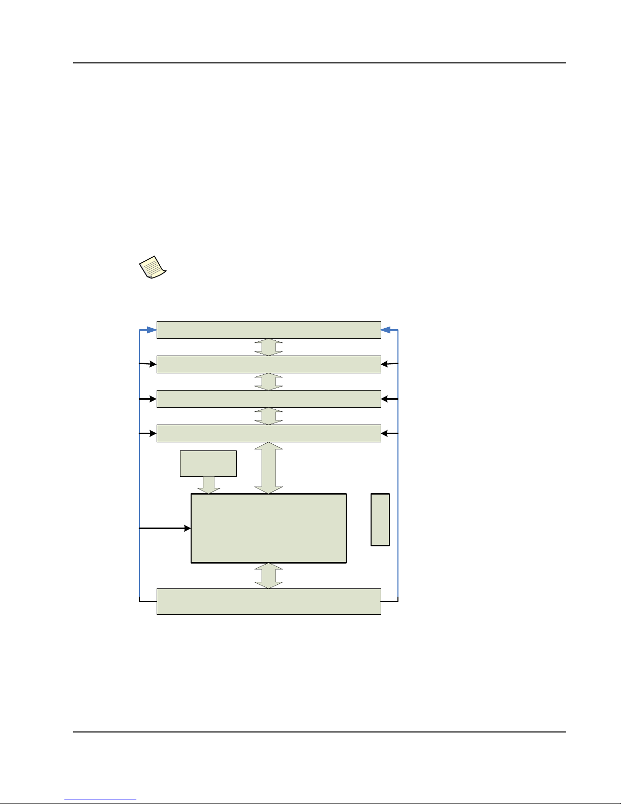
2.1 Overview
The Tsi340 PCI-to-PCI bridge evaluation board has the necessary functionality to evaluate all the
features of the Tsi340. The primary PCI side of the Tsi340 is wired to a PCI finger connector. The
secondary PCI side is wired to four, 32-bit, 3.3 V PCI connectors. Figure 1 shows the board block
diagram.
Many features can by exercised with shunt jumpers and switches.
Figure 1: Board Block Diagram
5
Integrated Device Technology
www.idt.com
Tsi340 Evaluation Board User Manual
80E3000_MA002_02
Page 6
6
P_CLK S_CLK_OUT0
S_CLK_OUT1
S_CLK_OUT2
S_CLK_OUT3
Tsi340
DIP
Switch
Secondary PCI
32bit 33/66MHz
Primary PCI
32bit 33/66MHz
PCI_M66EN
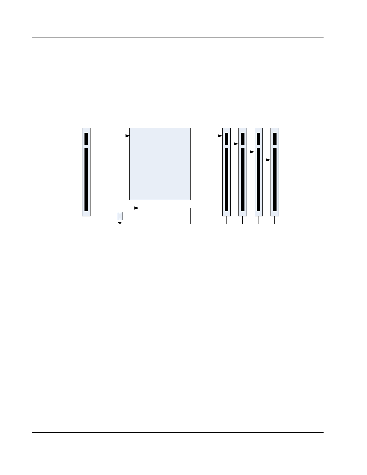
2.2 Clocking
Tsi340 is a synchronous device, where the secondary clock outputs are synchronous to the primary
clock input.
Figure 2 shows the PCI clocking connection.
Figure 2: Clock Signals
2.2.1 Domains
Primary and secondary clocking domains are described in the following sections.
2.2.1.1 Primary PCI Clock Domain
The primary clock is sourced from a PCI host. It must be synchronous with the primary PCI bus
(according to the PCI Specification (Revision 2.3))
The PCI host sets the clock frequency based on its M66EN signal level. However, the Tsi340
evaluation board has the option of forcing the PCI host's M66EN signal low with a DIP switch setting
on S1. Refer to “DIP Switch Package/ Individual Switch Position” on page 14 for more information.
2.2.1.2 Secondary PCI Clock Domain
T si340 has four secondary clock outputs, which provide PCI_CLKin for four on-board PCI connectors.
The secondary clock outputs are derived from the primary PCI clock input.
2.2.2 M66EN Signal
The M66EN signal from the primary side PCI finger connector is directly routed to four on-board PCI
connectors. A DIP switch is attached to M66EN that is used to force M66EN to ground so tha t the
33 MHz PCI clock can be set. Refer to “DIP Switch Package/ Individual Switch Position” on page 14
for more information.
Tsi340 Evaluation Board User Manual
80E3000_MA002_02
Integrated Device Technology
www.idt.com
Page 7

2.3 Arbitration
The T si340 has a built-in PCI arbiter for the secondary bus. The arbitration signals are connected to the
four PCI connectors on the board. Table 1 shows the Tsi340 arbitration signal assignment to each of
connectors.
Table 1: Arbitration Assignment
Tsi340 REQ/GNT Signals Connector
0J4
1J3
2J2
3J1
2.4 Power
The maximum current draw per rail for the bridge board with no cards plugged-in is indicated in
Table 2.
7
Table 2: Maximum Current Draw with No Plug-in Card
Rail Current
-12 V 0A
+12 V 0A
5V 0A
3.3 V <750mA
3.3 VAUX 0A
2.4.1 Finger Connector Current Limit
When plug-in cards are added to the Tsi340 evaluation board, the current draw must not exceed the
capacity of the finger connector. The maximum current draw per rail for the bridge board with cards
plugged-in is indicated in Table 3.
Integrated Device Technology
www.idt.com
Tsi340 Evaluation Board User Manual
80E3000_MA002_02
Page 8

8
The system user must limit its total power consumption to 25W budget from all power rails on the
primary finger connector based on PCI specification
Table 3: Maximum Current Draw Per Rail
Rail Current Power
-12V 100 mA 1.2 W
+12V 500 mA 6 W
5V 5 A 25 W
3.3V 7.6 A 25 W
3.3VAUX 375 mA 1.2W
2.4.1.1 Optional ATX Power Connector
If the total power requirement of plug-in cards exceed the current draw as indicated in Table 3, an
auxiliary ATX power supply may be used to augment the power capacity of the system. The bridge
board has an ATX power supply connector assembly option.
The ATX connector is usually not installed.
If the optional ATX power connector is used, the ATX power supply and PCI finger
connector supply must come from the same supply source.
2.4.2 Tsi340 Core Voltage Isolation
The T si340 supply voltage plane on the PCB can be isolated from th e boar d’s 3.3 V plane. This feature
is used to evaluate the current draw of the PCI bridge. The connection from the Tsi340 supply to the
board 3.3 V is done through three 0 Ohm resistors: R5, R6, R7. Current measurement can be done by
removing the resistors and insert an amp meter between the resistor pads on the PCB.
2.4.3 PRSNT Pin Power Setting on Primary PCI
The finger connector PRSNT[1:2] pins are wired to indicate a power requirement of 25 W. This is the
maximum power the PRSNT[1:2] pins can indicate for an add-in card. The PRSNT pin on the
secondary side connectors is not used.
Tsi340 Evaluation Board User Manual
80E3000_MA002_02
Integrated Device Technology
www.idt.com
Page 9

2.4.4 Primary and Secondary Side VIO
The bridge board can plug into a 3.3 V or 5 V system. The primary side input/output signalling uses the
same voltage as the system. The secondary side voltage is independent of the primary side voltage. The
secondary side signalling voltage is hard-wired to 3.3 V. If 5 V signalling is required on the secondary
side, the PCB assembly must be modified in the following ways:
• Remove the R1, R2, R3 resistors
• Solder jumper wires (AWG22) between the 5V test pads and the SVIO test pads.
Figure 3: Modified PCB Traces for 5 V Signaling on Secondary PCI Bus
9
Integrated Device Technology
www.idt.com
Tsi340 Evaluation Board User Manual
80E3000_MA002_02
Page 10

10
2.5 Interrupts and IDSEL
The add-in card interrupts are routed directly to the PCI system host. The Tsi340 is not involved with
interrupt routing. The connection of the interrupt lines from the PCI connectors to the finger connector
is arranged so that Int A of each PCI connector is routed to a different interrupt on the fin ger connect or.
Add-in card are numbered using AD[24:27] lines. Table 4 maps the interrupt connections designation
and AD line connections.
Table 4: Interrupt and IDSEL Mapping
Finger Connector Interrupt J1/AD27 J2/AD24 J3/AD25 J4/AD26
Int A Int B Int A Int D Int C
Int B Int C Int B Int A Int D
Int C Int D Int C Int B Int A
Int D Int A Int D Int C Int B
Table 5 shows the IDSEL assignments.
Table 5: Interrupt and IDSEL Mapping
Slot Number Bus Arbitration IDSEL Device ID
J1 REQ3/GNT3 IS_AD27 0xB P_INTB
J2 REQ2/GNT2 IS_AD26 0xA P_INTC
J3 REQ1/GNT1 IS_AD25 0x9 P_INTD
J4 REQ0/GNT0 IS_AD24 0x8 P_INTA
2.6 Resets
Tsi340 is reset from the system host reset signal (from the finger connector). The secondary side reset
is driven by Tsi340. There is no manual reset on the board.
INTA Routing to
Primary PCI
Tsi340 Evaluation Board User Manual
80E3000_MA002_02
Integrated Device Technology
www.idt.com
Page 11

3. Board Layout
In the board layout section of this document the component placement and the setting options are
explained.
3.1 PCB Layers
The Tsi340 Printed Circuit Board (PCB) stack up is made of the following four layers:
• Layer 1: PCB primary side (where most traces are routed)
• Layer 2: Ground plane
• Layer 3: Power plane
• Layer 4: Secondary side
Figure 4 shows the four layers of the PCB.
Figure 4: PCB Stack Up
11
Integrated Device Technology
www.idt.com
Tsi340 Evaluation Board User Manual
80E3000_MA002_02
Page 12

12
5.5”
7.87”
3.2 Board Dimensions
The board dimensions are based on PCI standard for a 32-bit Variable Height Short Add-in card.
However, the height of the card exceeds the maximum specified in the standard. The board dimensions
are shown in Figure 5.
Figure 5: Board Dimensions
Tsi340 Evaluation Board User Manual
80E3000_MA002_02
Integrated Device Technology
www.idt.com
Page 13

3.3 Component Placement
The placement of the components, jumpers, and switches are shown in Figure 6.
Figure 6: Component Placement
13
Integrated Device Technology
www.idt.com
Tsi340 Evaluation Board User Manual
80E3000_MA002_02
Page 14

14
ON
OFF
3.4 Switches
DIP switch S1 has eight slide switches, which are identified with numbers 1-to-8.
Figure 7: DIP Switch Package/ Individual Switch Position
Table 6 describes the settings for the S1 DIP switch..
Table 6: DIP Switch S1 Settings
S1 Description Default On/Off setting
1
Tsi340 P_CLKRUN# input pin
connection
2
Tsi340 LOO pin connection
3
P_RST# signal level
4
PCI_M66EN# signal level
5
Tsi340 S_CLKRUN# input pin
connection
6
Unused
7
Unused
8
Unused
ON
OFF
OFF
OFF
ON
OFF
OFF
OFF
ON: P_CLKRUN# is pulled down for normal operation.
OFF: P_CLKRUN# is pulled up for test purpose only.
ON: LOO is held low for test purpose only.
OFF: LOO is pulled up for normal operation.
ON: Force P_RST# to low for test purpose only.
OFF: Normal operation.
ON: Force PCI_M66EN to low for 33MHz clocking operation
OFF: Normal operation (PCI clock frequency is determined by primary
PCI_CLKin and PCI_M66EN# signal level from the secondary plug-in
cards)
ON: S_CLKRUN# is pulled down for normal operation.
OFF: S_CLKRUN# is pulled up for test purpose only.
OFF
OFF
OFF
Tsi340 Evaluation Board User Manual
80E3000_MA002_02
Integrated Device Technology
www.idt.com
Page 15

3.5 Connectors
Board connectors are used to add cards and power supplies to the Tsi340 board.
3.5.1 J1 through J4 Connectors - PCI Plug-in Card
J1, J2, J3, J4 are used to connect plug-in card on Tsi340’s secondary PCI side. The connector’s pin
assignment is standard PCI 32-bit, 3.3 V connectors.
15
Integrated Device Technology
www.idt.com
Tsi340 Evaluation Board User Manual
80E3000_MA002_02
Page 16

16
1
2
3
4
5
6
7
8
9
10
11
12
13
14
15
16
17
18
19
20
3.5.2 J5 - ATX Power Connector (Not Installed)
This connector is not installed on the Tsi340 board. This connector is only required if the voltage drop
at the plug-in card is to high. Table 11 shows the pin assignments for the J5 connector.
Table 7: J7 Pin Assignment
Pin Signal Assignment J7 pin location
13.3V
23.3V
3GND
45V
5GND
65V
7GND
8N/C
9N/C
10 12V
11 3.3V
12 -12V
13 GND
14 GND
15 GND
16 GND
17 GND
18 N/C
19 5V
20 5V
Tsi340 Evaluation Board User Manual
80E3000_MA002_02
Integrated Device Technology
www.idt.com
Page 17

3.5.3 Finger connector
The pin assignment for the finger connector are standard PCI 32-bit universal connectors.
The Finger connector JTAG signals TDI and TDO are connected together on the board.
3.6 LEDs
The LEDS on the board are used to identify the board activity shown in Table 8.
Table 8: LED description
LED Designation Signal Assignment Description
D1 5 V supply ON: 5 V supply is present
D2 3.3 V supply ON: 3.3 V supply is present
17
3.7 Test Points
Test points are provided on the Tsi340 board to facilitate signal probing.
3.7.1 Test Point for Clocks
The Tsi340 secondary clock outputs that are not used are brought out to test points. The clock test
points are listed in Table 9.
Table 9: Test Point for Clocks
Test point Signal Assignment
TP1 Ground
TP2 Ground
TP12 Ground
TP13 Ground
TP15 Ground
TP18 Ground
3.7.2 Test Point for Secondary VIO
The bridge board can plug into a 3.3 V or 5 V systems. The primary side input/output signaling uses
the same voltage as the system. The secondary side voltage is independent of the primary side voltage.
Integrated Device Technology
www.idt.com
Tsi340 Evaluation Board User Manual
80E3000_MA002_02
Page 18

18
4. Build of Materials (BOM)
Table 10: Tsi340 Evaluation Manual Build of Material
Item RefDes Part Number Manufacturer Description
1 C1,C3,C5-6,C8,
C10-12,C14,C16-18,
C20,C22-26,C39-43
2 C2,C4,C7,C9,C13,
C15,C19,C21,
C27-28,C33-34,C44,
C57-59,C61-63,
C66-68,C70-72, C74,
C78-79,C83
3 C29,C32,C35-36,
C45-56,C75,C77,
C80,C84-99
4 C30-31,C37-38,C73,
C76,C81-82
5 C60,C64-65,C69 0603ZD105KA T2A AVX X5R CER SMT, 1UF, +/-10%,
6 D1-2 HSMG-C150 AGILENT GREEN LED, UNTINTED,
7 J1 RBB60DHAS-S793 SULLINS PCI 3.3V, 32BIT, RIGHT
TAJA106K016 AVX TANT SMT, 10UF, +/-10%,
16V, 3216-18
06033D104MAT2A AVX X5R CER SMT, 0.1UF,
+/-20%, 25V, 0603
0603ZC103K AVX X7R CER SMT, 0.01UF,
+/-10%, 10V, 0603
GRM188R71H102MA01D MURATA X7R CER SMT, 0.001UF,
+/-20%, 50V, 0603
10V, 0603
DIFFUSED
ANGLE, 100MIL
ROW-TO-ROW
8 J2-4 145154-4 AMP PCI MOTHERBOARD,
32BIT, 3.3V, THRU
9 J5 39-29-9202 MOLEX ATX PWR JACK, 0.165"
PITCH, MINI-FIT JR
10 R1 ERJ-3EKF1103V PANA SONIC RES SMT, 110K OHM, 0.1W,
1%, 0603
11 R2-3,R28,R31,R35, R39 ERJ-3GEYJ151V PANASONI C RES SMT, 150 OHM, 0.1W,
5%, 0603
12 R4,R8, R10,R12, R14,
R16,R18-27,R29-30,
R32-34,R36-38, R40-42
13 R5-7,R17,R47 9C06031A0R00JLHFT YAGEO RES SMT, 0 OHM, 0.1W ,
14 R9,R11,R13,R15 ERJ-3GEYJ301V PANASONIC RES SMT, 300 OHM, 0.1W,
Tsi340 Evaluation Board User Manual
80E3000_MA002_02
ERJ-3GEYJ472V PANASONIC RES SMT, 4.7 KOHM, 0.1W,
5%, 0603
5%, 0603
5%, 0603
Integrated Device Technology
www.idt.com
Page 19

Table 10: Tsi340 Evaluation Manual Build of Material
Item RefDes Part Number Manufacturer Description
15 R43-46 ERJ-3GEYJ330V PANASONIC RES SMT, 33 OHM, 0.1W,
5%, 0603
16 S1 2-1437590-2 TYCO DIPSWITCH, 8 SWITCHES
17 TP1-16 TESTPOINT IDT Test points
18 U1 TSI340-66CQ IDT PCI TO PCI BRIDGE,
32BITS/66MHZ
19
Integrated Device Technology
www.idt.com
Tsi340 Evaluation Board User Manual
80E3000_MA002_02
Page 20

CORPORATE HEADQUARTERS
6024 Silver Creek Valley Road
San Jose, CA 95138
for SALES:
800-345-7015 or 408-284-8200
fax: 408-284-2775
www.idt.com
for Tech Support:
email: ssdhelp@idt.com
phone: 408-284-8208
document: 80E3000_MA002_02
September 19, 2009
 Loading...