

Page 1

Tsi310
User Manual
80B6020_MA001_05
®
IDT
™
PCI-X® Bridge
September 2009
6024 Silver Creek Valley Road, San Jose, California 95138
Telephone: (800) 345-7015 • (408) 284-8200 • FAX: (408) 284-2775
©2009 Integrated Device Technology, Inc.
Printed in U.S.A.
Page 2

Integrated Device Technology, Inc. reserves the right to make changes to its products or specifications at any time, without notice, in order to improve design or performance
and to supply the best possible product. IDT does not assume any responsibility for use of any circuitry described other than the circuitry embodied in an IDT product. The
Company makes no representations that circuitry described herein is free from patent infringement or other rights of third parties which may result from its use. No license is
granted by implication or otherwise under any patent, patent rights or other rights, of Integrated Device Technology, Inc.
GENERAL DISCLAIMER
Code examples provided by IDT are for illustrative purposes only and should not be relied upon for developing applications. Any use of the code examples below is completely
at your own risk. IDT MAKES NO REPRESENT ATIONS OR WARRANTIES OF ANY KIND CONCERNING THE NONINFRINGEMENT, QUALITY, SAFETY OR SUITABILITY
OF THE CODE, EITHER EXPRESS OR IMPLIED, INCLUDING WITHOUT LIMITATION ANY IMPLIED WARRANTIES OF MERCHANTABILITY, FITNESS FOR A PARTICULAR PURPOSE, OR NON-INFRINGEMENT. FURTHER, IDT MAKES NO REPRESENT ATIONS OR WARRANTIES AS TO THE TRUTH, ACCURACY OR COMPLETENESS
OF ANY STATEMENTS, INFORMATION OR MATERIALS CONCERNING CODE EXAMPLES CONTAINED IN ANY IDT PUBLICATION OR PUBLIC DISCLOSURE OR
THAT IS CONTAINED ON ANY IDT INTERNET SITE. IN NO EVENT WILL IDT BE LIABLE FOR ANY DIRECT, CONSEQUENTIAL, I NCIDENTAL, INDIRECT, PUNITIVE OR
SPECIAL DAMAGES, HOWEVER THEY MAY ARIS E, AND EVEN IF IDT HAS BEEN PREVIOUSLY ADVISED ABOUT THE POSSIBILITY OF SUCH DAMAGES. The code
examples also may be subject to United States export control laws and may be subject to the export or import laws of other countries and it is your responsibility to comply with
any applicable laws or regulations.
Integrated Device Technology's products are not authorized for use as critical components in life support devices or systems unless a specific written agreement pertaining to
such intended use is executed between the manufacturer and an officer of IDT.
1. Life support devices or systems are devices or systems which (a) are intended for surgical implant into the body or (b) support or sustain life and whose failure to perform,
when properly used in accordance with instructions for use provided in the labeling, can be reasonably expected to result in a significant injury to the user.
2. A critical component is any components of a life support device or system whose failure to perform can be reasonably expected to cause the failure of the life support device
or system, or to affect its safety or effectiveness.
IDT, the IDT logo, and Integrated Device Technology are trademarks or registered trademarks of Integrated Device Technology, Inc.
CODE DISCLAIMER
LIFE SUPPORT POLICY
Page 3

Contents
About this Document. . . . . . . . . . . . . . . . . . . . . . . . . . . . . . . . . . . . . . . . . . . . . . . . . . . . 13
Revision History . . . . . . . . . . . . . . . . . . . . . . . . . . . . . . . . . . . . . . . . . . . . . . . . . . . . . . . . . . . . . . . . . . . 13
Document Conventions . . . . . . . . . . . . . . . . . . . . . . . . . . . . . . . . . . . . . . . . . . . . . . . . . . . . . . . . . . . . . 14
Related Information . . . . . . . . . . . . . . . . . . . . . . . . . . . . . . . . . . . . . . . . . . . . . . . . . . . . . . . . . . . . . . . . 17
1. Functional Overview . . . . . . . . . . . . . . . . . . . . . . . . . . . . . . . . . . . . . . . . . . . . . . . . 19
1.1 Overview of the Tsi310 . . . . . . . . . . . . . . . . . . . . . . . . . . . . . . . . . . . . . . . . . . . . . . . . . . . . . . . . 19
1.2 Features. . . . . . . . . . . . . . . . . . . . . . . . . . . . . . . . . . . . . . . . . . . . . . . . . . . . . . . . . . . . . . . . . . . . . 22
1.2.1 PCI-X Interfaces . . . . . . . . . . . . . . . . . . . . . . . . . . . . . . . . . . . . . . . . . . . . . . . . . . . . . . 22
1.2.2 Memory Buffer Architecture . . . . . . . . . . . . . . . . . . . . . . . . . . . . . . . . . . . . . . . . . . . . 22
1.2.3 Power Management. . . . . . . . . . . . . . . . . . . . . . . . . . . . . . . . . . . . . . . . . . . . . . . . . . . . 22
1.2.4 Transaction Forwarding . . . . . . . . . . . . . . . . . . . . . . . . . . . . . . . . . . . . . . . . . . . . . . . . 23
1.2.5 Configuration Registers . . . . . . . . . . . . . . . . . . . . . . . . . . . . . . . . . . . . . . . . . . . . . . . . 23
3
1.2.6 Optional Features . . . . . . . . . . . . . . . . . . . . . . . . . . . . . . . . . . . . . . . . . . . . . . . . . . . . . 23
1.2.7 Bus Arbitration . . . . . . . . . . . . . . . . . . . . . . . . . . . . . . . . . . . . . . . . . . . . . . . . . . . . . . . 23
1.2.8 IEEE
®
1149.1 JTAG Port . . . . . . . . . . . . . . . . . . . . . . . . . . . . . . . . . . . . . . . . . . . . . . . 23
1.3 Operation Overview . . . . . . . . . . . . . . . . . . . . . . . . . . . . . . . . . . . . . . . . . . . . . . . . . . . . . . . . . . . 24
1.3.1 Supported Modes . . . . . . . . . . . . . . . . . . . . . . . . . . . . . . . . . . . . . . . . . . . . . . . . . . . . . 24
1.3.2 Buffer Structure. . . . . . . . . . . . . . . . . . . . . . . . . . . . . . . . . . . . . . . . . . . . . . . . . . . . . . . 24
1.3.3 Address Decoding. . . . . . . . . . . . . . . . . . . . . . . . . . . . . . . . . . . . . . . . . . . . . . . . . . . . . 25
1.3.4 Bus Arbitration . . . . . . . . . . . . . . . . . . . . . . . . . . . . . . . . . . . . . . . . . . . . . . . . . . . . . . . 26
1.4 Technology Highlights . . . . . . . . . . . . . . . . . . . . . . . . . . . . . . . . . . . . . . . . . . . . . . . . . . . . . . . . . 26
2. Bus Operation. . . . . . . . . . . . . . . . . . . . . . . . . . . . . . . . . . . . . . . . . . . . . . . . . . . . . . 27
2.1 Overview of Bus Operation . . . . . . . . . . . . . . . . . . . . . . . . . . . . . . . . . . . . . . . . . . . . . . . . . . . . . 27
2.1.1 Types of Transactions . . . . . . . . . . . . . . . . . . . . . . . . . . . . . . . . . . . . . . . . . . . . . . . . . . 28
2.2 Write Transactions . . . . . . . . . . . . . . . . . . . . . . . . . . . . . . . . . . . . . . . . . . . . . . . . . . . . . . . . . . . . 30
2.2.1 Posted Write Transactions. . . . . . . . . . . . . . . . . . . . . . . . . . . . . . . . . . . . . . . . . . . . . . . 30
2.2.2 Delayed/Split Write Transactions . . . . . . . . . . . . . . . . . . . . . . . . . . . . . . . . . . . . . . . . . 32
2.2.3 Immediate Write Transactions . . . . . . . . . . . . . . . . . . . . . . . . . . . . . . . . . . . . . . . . . . . 32
2.3 Read Transactions. . . . . . . . . . . . . . . . . . . . . . . . . . . . . . . . . . . . . . . . . . . . . . . . . . . . . . . . . . . . . 33
2.3.1 Memory Read Transactions . . . . . . . . . . . . . . . . . . . . . . . . . . . . . . . . . . . . . . . . . . . . . 33
2.3.2 I/O Read . . . . . . . . . . . . . . . . . . . . . . . . . . . . . . . . . . . . . . . . . . . . . . . . . . . . . . . . . . . . 35
2.3.3 Configuration Read. . . . . . . . . . . . . . . . . . . . . . . . . . . . . . . . . . . . . . . . . . . . . . . . . . . . 35
Tsi310 User Manual
80B6020_MA001_05
Page 4

Contents4
2.3.4 Non-Prefetchable and DWord Reads. . . . . . . . . . . . . . . . . . . . . . . . . . . . . . . . . . . . . . .35
2.3.5 Prefetchable Reads . . . . . . . . . . . . . . . . . . . . . . . . . . . . . . . . . . . . . . . . . . . . . . . . . . . . 36
2.4 Configuration Transactions. . . . . . . . . . . . . . . . . . . . . . . . . . . . . . . . . . . . . . . . . . . . . . . . . . . . . .37
2.4.1 Configuration Type 0 Access to Bridge . . . . . . . . . . . . . . . . . . . . . . . . . . . . . . . . . . . . 38
2.4.2 Type 1 to Type 0 Translation by Bridge . . . . . . . . . . . . . . . . . . . . . . . . . . . . . . . . . . . . 40
2.4.3 Type 1 to Type 1 Forwarding by Bridge . . . . . . . . . . . . . . . . . . . . . . . . . . . . . . . . . . . . 42
2.4.4 Special Cycle Generation by the Bridge . . . . . . . . . . . . . . . . . . . . . . . . . . . . . . . . . . . . 42
3. Clocking and Reset Options. . . . . . . . . . . . . . . . . . . . . . . . . . . . . . . . . . . . . . . . . . .45
3.1 Clocking Domains. . . . . . . . . . . . . . . . . . . . . . . . . . . . . . . . . . . . . . . . . . . . . . . . . . . . . . . . . . . . . 45
3.2 Clock Jitter . . . . . . . . . . . . . . . . . . . . . . . . . . . . . . . . . . . . . . . . . . . . . . . . . . . . . . . . . . . . . . . . . . 46
3.3 Mode and Clock Frequency Determination . . . . . . . . . . . . . . . . . . . . . . . . . . . . . . . . . . . . . . . . . 46
3.3.1 Primary Interface. . . . . . . . . . . . . . . . . . . . . . . . . . . . . . . . . . . . . . . . . . . . . . . . . . . . . .46
3.3.2 Secondary Interface. . . . . . . . . . . . . . . . . . . . . . . . . . . . . . . . . . . . . . . . . . . . . . . . . . . . 47
3.4 Clock Stability. . . . . . . . . . . . . . . . . . . . . . . . . . . . . . . . . . . . . . . . . . . . . . . . . . . . . . . . . . . . . . . .48
3.5 Driver Impedance Selection . . . . . . . . . . . . . . . . . . . . . . . . . . . . . . . . . . . . . . . . . . . . . . . . . . . . .49
3.6 Reset Functions and Operations . . . . . . . . . . . . . . . . . . . . . . . . . . . . . . . . . . . . . . . . . . . . . . . . . . 50
3.6.1 Primary Reset . . . . . . . . . . . . . . . . . . . . . . . . . . . . . . . . . . . . . . . . . . . . . . . . . . . . . . . . 50
3.6.2 Secondary Reset . . . . . . . . . . . . . . . . . . . . . . . . . . . . . . . . . . . . . . . . . . . . . . . . . . . . . .51
3.7 Bus Parking and Bus Width Determination . . . . . . . . . . . . . . . . . . . . . . . . . . . . . . . . . . . . . . . . . 53
3.8 Power Management and Hot-Plug . . . . . . . . . . . . . . . . . . . . . . . . . . . . . . . . . . . . . . . . . . . . . . . .54
3.9 Secondary Device Masking. . . . . . . . . . . . . . . . . . . . . . . . . . . . . . . . . . . . . . . . . . . . . . . . . . . . . . 55
3.10 Handling of Address Phase Parity Errors . . . . . . . . . . . . . . . . . . . . . . . . . . . . . . . . . . . . . . . . . . .55
3.11 Optional Base Address Register . . . . . . . . . . . . . . . . . . . . . . . . . . . . . . . . . . . . . . . . . . . . . . . . . . 55
3.12 Optional Configuration Register Access from the Secondary Bus. . . . . . . . . . . . . . . . . . . . . . . .56
3.13 Short Term Caching . . . . . . . . . . . . . . . . . . . . . . . . . . . . . . . . . . . . . . . . . . . . . . . . . . . . . . . . . . . 57
4. Transaction Ordering . . . . . . . . . . . . . . . . . . . . . . . . . . . . . . . . . . . . . . . . . . . . . . . .59
4.1 Overview of Transaction Ordering . . . . . . . . . . . . . . . . . . . . . . . . . . . . . . . . . . . . . . . . . . . . . . . . 59
4.2 General Ordering Guidelines . . . . . . . . . . . . . . . . . . . . . . . . . . . . . . . . . . . . . . . . . . . . . . . . . . . . 59
4.3 Ordering Rules . . . . . . . . . . . . . . . . . . . . . . . . . . . . . . . . . . . . . . . . . . . . . . . . . . . . . . . . . . . . . . . 60
5. Configuration Registers . . . . . . . . . . . . . . . . . . . . . . . . . . . . . . . . . . . . . . . . . . . . . .63
5.1 Overview of Registers . . . . . . . . . . . . . . . . . . . . . . . . . . . . . . . . . . . . . . . . . . . . . . . . . . . . . . . . . 63
5.1.1 Terms and Abbreviations. . . . . . . . . . . . . . . . . . . . . . . . . . . . . . . . . . . . . . . . . . . . . . . .63
5.1.2 Configuration Space . . . . . . . . . . . . . . . . . . . . . . . . . . . . . . . . . . . . . . . . . . . . . . . . . . . 64
5.1.3 Type 1 PCI Configuration Space Header . . . . . . . . . . . . . . . . . . . . . . . . . . . . . . . . . . .64
5.2 Register Map. . . . . . . . . . . . . . . . . . . . . . . . . . . . . . . . . . . . . . . . . . . . . . . . . . . . . . . . . . . . . . . . . 65
Tsi310 User Manual
80B6020_MA001_05
Page 5

Contents 5
5.3 Register Summary . . . . . . . . . . . . . . . . . . . . . . . . . . . . . . . . . . . . . . . . . . . . . . . . . . . . . . . . . . . . 68
5.4 PCI Configuration Space Header Registers . . . . . . . . . . . . . . . . . . . . . . . . . . . . . . . . . . . . . . . . . 71
5.4.1 Vendor ID Register . . . . . . . . . . . . . . . . . . . . . . . . . . . . . . . . . . . . . . . . . . . . . . . . . . . . 71
5.4.2 Device ID Register . . . . . . . . . . . . . . . . . . . . . . . . . . . . . . . . . . . . . . . . . . . . . . . . . . . . 72
5.4.3 Command Register . . . . . . . . . . . . . . . . . . . . . . . . . . . . . . . . . . . . . . . . . . . . . . . . . . . . 73
5.4.4 Status Register. . . . . . . . . . . . . . . . . . . . . . . . . . . . . . . . . . . . . . . . . . . . . . . . . . . . . . . . 75
5.4.5 Revision ID Register. . . . . . . . . . . . . . . . . . . . . . . . . . . . . . . . . . . . . . . . . . . . . . . . . . . 77
5.4.6 Class Code Register . . . . . . . . . . . . . . . . . . . . . . . . . . . . . . . . . . . . . . . . . . . . . . . . . . . 77
5.4.7 Cache Line Size Register . . . . . . . . . . . . . . . . . . . . . . . . . . . . . . . . . . . . . . . . . . . . . . . 78
5.4.8 Latency Timer Register. . . . . . . . . . . . . . . . . . . . . . . . . . . . . . . . . . . . . . . . . . . . . . . . . 79
5.4.9 Header Type Register . . . . . . . . . . . . . . . . . . . . . . . . . . . . . . . . . . . . . . . . . . . . . . . . . . 80
5.4.10 BIST Register . . . . . . . . . . . . . . . . . . . . . . . . . . . . . . . . . . . . . . . . . . . . . . . . . . . . . . . . 80
5.4.11 Lower Memory Base Address Register . . . . . . . . . . . . . . . . . . . . . . . . . . . . . . . . . . . . 81
5.4.12 Upper Memory Base Address Register. . . . . . . . . . . . . . . . . . . . . . . . . . . . . . . . . . . . . 83
5.4.13 Primary Bus Number Register . . . . . . . . . . . . . . . . . . . . . . . . . . . . . . . . . . . . . . . . . . . 84
5.4.14 Secondar y Bus Number Register . . . . . . . . . . . . . . . . . . . . . . . . . . . . . . . . . . . . . . . . . 85
5.4.15 Subordinate Bus Number Register . . . . . . . . . . . . . . . . . . . . . . . . . . . . . . . . . . . . . . . . 86
5.4.16 Secondary Latency Timer Register. . . . . . . . . . . . . . . . . . . . . . . . . . . . . . . . . . . . . . . . 87
5.4.17 I/O Base Register . . . . . . . . . . . . . . . . . . . . . . . . . . . . . . . . . . . . . . . . . . . . . . . . . . . . . 88
5.4.18 I/O Limit Register. . . . . . . . . . . . . . . . . . . . . . . . . . . . . . . . . . . . . . . . . . . . . . . . . . . . . 89
5.4.19 Secondary Status Register. . . . . . . . . . . . . . . . . . . . . . . . . . . . . . . . . . . . . . . . . . . . . . . 90
5.4.20 Memory Base Register . . . . . . . . . . . . . . . . . . . . . . . . . . . . . . . . . . . . . . . . . . . . . . . . . 92
5.4.21 Memory Limit Register. . . . . . . . . . . . . . . . . . . . . . . . . . . . . . . . . . . . . . . . . . . . . . . . . 93
5.4.22 Prefetchable Memory Base Register. . . . . . . . . . . . . . . . . . . . . . . . . . . . . . . . . . . . . . . 94
5.4.23 Prefetchable Memory Limit Register . . . . . . . . . . . . . . . . . . . . . . . . . . . . . . . . . . . . . . 95
5.4.24 Prefetchable Base Upper 32 Bits Register . . . . . . . . . . . . . . . . . . . . . . . . . . . . . . . . . . 96
5.4.25 Prefetchable Limit Upper 32 Bits Register. . . . . . . . . . . . . . . . . . . . . . . . . . . . . . . . . . 97
5.4.26 I/O Base Upper 16 Bits Register. . . . . . . . . . . . . . . . . . . . . . . . . . . . . . . . . . . . . . . . . . 98
5.4.27 I/O Limit Upper 16 Bits Register . . . . . . . . . . . . . . . . . . . . . . . . . . . . . . . . . . . . . . . . . 99
5.4.28 Capabilities Pointer Register. . . . . . . . . . . . . . . . . . . . . . . . . . . . . . . . . . . . . . . . . . . . 100
5.4.29 Reserved Registers . . . . . . . . . . . . . . . . . . . . . . . . . . . . . . . . . . . . . . . . . . . . . . . . . . . 100
5.4.30 Interrupt Line Register . . . . . . . . . . . . . . . . . . . . . . . . . . . . . . . . . . . . . . . . . . . . . . . . 101
5.4.31 Interrupt Pin Register . . . . . . . . . . . . . . . . . . . . . . . . . . . . . . . . . . . . . . . . . . . . . . . . . 101
5.4.32 Bridge Control Register . . . . . . . . . . . . . . . . . . . . . . . . . . . . . . . . . . . . . . . . . . . . . . . 102
5.5 Device-Specific Configuration Space Registers. . . . . . . . . . . . . . . . . . . . . . . . . . . . . . . . . . . . . 105
5.5.1 Primary Data Buffering Control Register. . . . . . . . . . . . . . . . . . . . . . . . . . . . . . . . . . 105
Tsi310 User Manual
80B6020_MA001_05
Page 6

Contents6
5.5.2 Secondary Data Buffering Control Register . . . . . . . . . . . . . . . . . . . . . . . . . . . . . . . . 108
5.5.3 Miscellaneous Control Register . . . . . . . . . . . . . . . . . . . . . . . . . . . . . . . . . . . . . . . . . 111
5.5.4 Arbiter Mode Register. . . . . . . . . . . . . . . . . . . . . . . . . . . . . . . . . . . . . . . . . . . . . . . . . 113
5.5.5 Arbiter Enable Register. . . . . . . . . . . . . . . . . . . . . . . . . . . . . . . . . . . . . . . . . . . . . . . . 115
5.5.6 Arbiter Priority Register . . . . . . . . . . . . . . . . . . . . . . . . . . . . . . . . . . . . . . . . . . . . . . . 117
5.5.7 SERR# Disable Register . . . . . . . . . . . . . . . . . . . . . . . . . . . . . . . . . . . . . . . . . . . . . . . 119
5.5.8 Primary Retry Counter Register . . . . . . . . . . . . . . . . . . . . . . . . . . . . . . . . . . . . . . . . .1 21
5.5.9 Secondary Retry Counter Register . . . . . . . . . . . . . . . . . . . . . . . . . . . . . . . . . . . . . . .123
5.5.10 Discard Timer Control Register. . . . . . . . . . . . . . . . . . . . . . . . . . . . . . . . . . . . . . . . . . 125
5.5.11 Retry and Timer Status Register . . . . . . . . . . . . . . . . . . . . . . . . . . . . . . . . . . . . . . . . . 127
5.5.12 Opaque Memory Enable Register . . . . . . . . . . . . . . . . . . . . . . . . . . . . . . . . . . . . . . . . 128
5.5.13 Opaque Memory Base Register. . . . . . . . . . . . . . . . . . . . . . . . . . . . . . . . . . . . . . . . . . 129
5.5.14 Opaque Memory Limit Register . . . . . . . . . . . . . . . . . . . . . . . . . . . . . . . . . . . . . . . . . 130
5.5.15 Opaque Memory Base Upper 32 Bits Register . . . . . . . . . . . . . . . . . . . . . . . . . . . . . . 131
5.5.16 Opaque Memory Limit Upper 32 Bits Register . . . . . . . . . . . . . . . . . . . . . . . . . . . . . 132
5.5.17 PCI-X ID Register . . . . . . . . . . . . . . . . . . . . . . . . . . . . . . . . . . . . . . . . . . . . . . . . . . . . 133
5.5.18 Next Capabilities Pointer Register . . . . . . . . . . . . . . . . . . . . . . . . . . . . . . . . . . . . . . . 134
5.5.19 PCI-X Secondary Status Register . . . . . . . . . . . . . . . . . . . . . . . . . . . . . . . . . . . . . . . . 135
5.5.20 PCI-X Bridge Status Register . . . . . . . . . . . . . . . . . . . . . . . . . . . . . . . . . . . . . . . . . . .137
5.5.21 Secondary Bus Upstream Split Transaction Register . . . . . . . . . . . . . . . . . . . . . . . . .140
5.5.22 Primary Bus Downstream Split Transaction Register. . . . . . . . . . . . . . . . . . . . . . . . .141
5.5.23 Power Management ID Register . . . . . . . . . . . . . . . . . . . . . . . . . . . . . . . . . . . . . . . . . 142
5.5.24 Next Capabilities Pointer Register . . . . . . . . . . . . . . . . . . . . . . . . . . . . . . . . . . . . . . . 142
5.5.25 Power Management Capabilities Register. . . . . . . . . . . . . . . . . . . . . . . . . . . . . . . . . . 143
5.5.26 Power Management Control/Status Register. . . . . . . . . . . . . . . . . . . . . . . . . . . . . . . . 144
5.5.27 PCI-to-PCI Bridge Support Extensions Register . . . . . . . . . . . . . . . . . . . . . . . . . . . . 145
5.5.28 Data Register . . . . . . . . . . . . . . . . . . . . . . . . . . . . . . . . . . . . . . . . . . . . . . . . . . . . . . . . 145
5.5.29 Secondary Bus Private Device Mask Register . . . . . . . . . . . . . . . . . . . . . . . . . . . . . .146
5.5.30 Miscellaneous Control Register 2 . . . . . . . . . . . . . . . . . . . . . . . . . . . . . . . . . . . . . . . . 148
6. Signals and Pinout . . . . . . . . . . . . . . . . . . . . . . . . . . . . . . . . . . . . . . . . . . . . . . . . .151
6.1 Overview of Signals and Pinout . . . . . . . . . . . . . . . . . . . . . . . . . . . . . . . . . . . . . . . . . . . . . . . . . 151
6.2 Primary Interface Signals . . . . . . . . . . . . . . . . . . . . . . . . . . . . . . . . . . . . . . . . . . . . . . . . . . . . . . 151
6.3 Secondary Interface Signals . . . . . . . . . . . . . . . . . . . . . . . . . . . . . . . . . . . . . . . . . . . . . . . . . . . .154
6.4 Strapping Pins and Other Signals . . . . . . . . . . . . . . . . . . . . . . . . . . . . . . . . . . . . . . . . . . . . . . . . 157
6.5 Test Signals . . . . . . . . . . . . . . . . . . . . . . . . . . . . . . . . . . . . . . . . . . . . . . . . . . . . . . . . . . . . . . . . . 160
6.6 Power and Ground Connections . . . . . . . . . . . . . . . . . . . . . . . . . . . . . . . . . . . . . . . . . . . . . . . . .161
Tsi310 User Manual
80B6020_MA001_05
Page 7

Contents 7
6.6.1 Filter Requirements for P_VDDA and S_VDDA . . . . . . . . . . . . . . . . . . . . . . . . . . . . 161
6.7 Pinout . . . . . . . . . . . . . . . . . . . . . . . . . . . . . . . . . . . . . . . . . . . . . . . . . . . . . . . . . . . . . . . . . . . . . 163
6.7.1 Pinout — Sorted by Signal Name. . . . . . . . . . . . . . . . . . . . . . . . . . . . . . . . . . . . . . . . 164
6.7.2 Pinout — Sorted by Grid Position . . . . . . . . . . . . . . . . . . . . . . . . . . . . . . . . . . . . . . . 167
7. JTAG Boundary Scan. . . . . . . . . . . . . . . . . . . . . . . . . . . . . . . . . . . . . . . . . . . . . . . 171
7.1 Overview of JTAG Boundary Scan . . . . . . . . . . . . . . . . . . . . . . . . . . . . . . . . . . . . . . . . . . . . . . 171
7.2 TAP Controller Initialization . . . . . . . . . . . . . . . . . . . . . . . . . . . . . . . . . . . . . . . . . . . . . . . . . . . 172
7.3 JTAG Design Considerations . . . . . . . . . . . . . . . . . . . . . . . . . . . . . . . . . . . . . . . . . . . . . . . . . . . 172
7.3.1 Including the Tsi310 in a JTAG Scan Ring. . . . . . . . . . . . . . . . . . . . . . . . . . . . . . . . . 172
7.3.2 Excluding the Tsi310 from a JTAG Scan Ring. . . . . . . . . . . . . . . . . . . . . . . . . . . . . . 172
7.4 Instruction Register and Codes. . . . . . . . . . . . . . . . . . . . . . . . . . . . . . . . . . . . . . . . . . . . . . . . . . 173
7.5 Bypass Register . . . . . . . . . . . . . . . . . . . . . . . . . . . . . . . . . . . . . . . . . . . . . . . . . . . . . . . . . . . . . 173
7.6 JTAG Device ID Register. . . . . . . . . . . . . . . . . . . . . . . . . . . . . . . . . . . . . . . . . . . . . . . . . . . . . . 174
7.7 Boundary Scan Register . . . . . . . . . . . . . . . . . . . . . . . . . . . . . . . . . . . . . . . . . . . . . . . . . . . . . . . 174
7.7.1 Boundary Scan Register Bit Map . . . . . . . . . . . . . . . . . . . . . . . . . . . . . . . . . . . . . . . . 175
8. Electrical Characteristics . . . . . . . . . . . . . . . . . . . . . . . . . . . . . . . . . . . . . . . . . . . 191
8.1 PCI/PCI-X Specification Conformance . . . . . . . . . . . . . . . . . . . . . . . . . . . . . . . . . . . . . . . . . . . 191
8.2 Absolute Maximum Ratings. . . . . . . . . . . . . . . . . . . . . . . . . . . . . . . . . . . . . . . . . . . . . . . . . . . . 192
8.3 Recommended DC Operating Conditions . . . . . . . . . . . . . . . . . . . . . . . . . . . . . . . . . . . . . . . . . 193
8.4 AC Operating Conditions. . . . . . . . . . . . . . . . . . . . . . . . . . . . . . . . . . . . . . . . . . . . . . . . . . . . . . 193
8.5 Power Dissipation. . . . . . . . . . . . . . . . . . . . . . . . . . . . . . . . . . . . . . . . . . . . . . . . . . . . . . . . . . . . 194
9. Package Information . . . . . . . . . . . . . . . . . . . . . . . . . . . . . . . . . . . . . . . . . . . . . . . 197
9.1 Package Characteristics . . . . . . . . . . . . . . . . . . . . . . . . . . . . . . . . . . . . . . . . . . . . . . . . . . . . . . . 197
9.2 Thermal Characteristics . . . . . . . . . . . . . . . . . . . . . . . . . . . . . . . . . . . . . . . . . . . . . . . . . . . . . . . 199
A. Ordering Information . . . . . . . . . . . . . . . . . . . . . . . . . . . . . . . . . . . . . . . . . . . . . . . 201
A.1 Ordering Information . . . . . . . . . . . . . . . . . . . . . . . . . . . . . . . . . . . . . . . . . . . . . . . . . . . . . . . . . 201
Index . . . . . . . . . . . . . . . . . . . . . . . . . . . . . . . . . . . . . . . . . . . . . . . . . . . . . . . . . . . . . . . . 203
Tsi310 User Manual
80B6020_MA001_05
Page 8

Contents8
Tsi310 User Manual
80B6020_MA001_05
Page 9

List of Figures
Figure 1: Block Diagram . . . . . . . . . . . . . . . . . . . . . . . . . . . . . . . . . . . . . . . . . . . . . . . . . . . . . . . . . . . . . . . 20
Figure 2: Configuration Transaction Address Formats . . . . . . . . . . . . . . . . . . . . . . . . . . . . . . . . . . . . . . . . 38
Figure 3: Programmable Pull-up Circuit. . . . . . . . . . . . . . . . . . . . . . . . . . . . . . . . . . . . . . . . . . . . . . . . . . . . 48
Figure 4: De-assertion of S_RST# . . . . . . . . . . . . . . . . . . . . . . . . . . . . . . . . . . . . . . . . . . . . . . . . . . . . . . . . 52
Figure 5: Filter Requirements for P_VDDA and S_VDDA. . . . . . . . . . . . . . . . . . . . . . . . . . . . . . . . . . . . 161
Figure 6: Inductor L1 Impedance . . . . . . . . . . . . . . . . . . . . . . . . . . . . . . . . . . . . . . . . . . . . . . . . . . . . . . . . 162
Figure 7: Pinout — Viewed from Above (Looking Through the Device). . . . . . . . . . . . . . . . . . . . . . . . . 163
Figure 8: Package Diagram. . . . . . . . . . . . . . . . . . . . . . . . . . . . . . . . . . . . . . . . . . . . . . . . . . . . . . . . . . . . . 198
9
Tsi310 User Manual
80B6020_MA001_05
Page 10

List of Figures10
Tsi310 User Manual
80B6020_MA001_05
Page 11

List of Tables
Table 1: PCI Transactions . . . . . . . . . . . . . . . . . . . . . . . . . . . . . . . . . . . . . . . . . . . . . . . . . . . . . . . . . . . . . . 28
Table 2: PCI-X Transactions. . . . . . . . . . . . . . . . . . . . . . . . . . . . . . . . . . . . . . . . . . . . . . . . . . . . . . . . . . . . 29
Table 3: Write Transaction Handling . . . . . . . . . . . . . . . . . . . . . . . . . . . . . . . . . . . . . . . . . . . . . . . . . . . . . 30
Table 4: Read Transaction Handling. . . . . . . . . . . . . . . . . . . . . . . . . . . . . . . . . . . . . . . . . . . . . . . . . . . . . . 33
Table 5: IDSEL Generation. . . . . . . . . . . . . . . . . . . . . . . . . . . . . . . . . . . . . . . . . . . . . . . . . . . . . . . . . . . . . 41
Table 6: Driver Impedance Selection . . . . . . . . . . . . . . . . . . . . . . . . . . . . . . . . . . . . . . . . . . . . . . . . . . . . . 50
Table 7: Delay Times for De-assertion of S_RST#. . . . . . . . . . . . . . . . . . . . . . . . . . . . . . . . . . . . . . . . . . . 53
Table 8: Tsi310 Ordering Rules — PCI-X Mode . . . . . . . . . . . . . . . . . . . . . . . . . . . . . . . . . . . . . . . . . . . . 60
Table 9: Tsi310 Ordering Rules — PCI Mode . . . . . . . . . . . . . . . . . . . . . . . . . . . . . . . . . . . . . . . . . . . . . . 61
Table 10: Register Terms . . . . . . . . . . . . . . . . . . . . . . . . . . . . . . . . . . . . . . . . . . . . . . . . . . . . . . . . . . . . . . . 63
Table 11: Register Map . . . . . . . . . . . . . . . . . . . . . . . . . . . . . . . . . . . . . . . . . . . . . . . . . . . . . . . . . . . . . . . . . 65
Table 12: Register Summary. . . . . . . . . . . . . . . . . . . . . . . . . . . . . . . . . . . . . . . . . . . . . . . . . . . . . . . . . . . . . 68
11
Table 13: Primary Interface Signals . . . . . . . . . . . . . . . . . . . . . . . . . . . . . . . . . . . . . . . . . . . . . . . . . . . . . . 151
Table 14: Secondary Interface Signals . . . . . . . . . . . . . . . . . . . . . . . . . . . . . . . . . . . . . . . . . . . . . . . . . . . . 154
Table 15: Strapping Pins and Other Signals . . . . . . . . . . . . . . . . . . . . . . . . . . . . . . . . . . . . . . . . . . . . . . . . 157
Table 16: Test Signals . . . . . . . . . . . . . . . . . . . . . . . . . . . . . . . . . . . . . . . . . . . . . . . . . . . . . . . . . . . . . . . . . 160
Table 17: Power and Ground Connections . . . . . . . . . . . . . . . . . . . . . . . . . . . . . . . . . . . . . . . . . . . . . . . . . 161
Table 18: Inductor L1 Characteristics. . . . . . . . . . . . . . . . . . . . . . . . . . . . . . . . . . . . . . . . . . . . . . . . . . . . . 162
Table 19: Signal Pin Listing by Signal Name . . . . . . . . . . . . . . . . . . . . . . . . . . . . . . . . . . . . . . . . . . . . . . . 164
Table 20: Signal Pin Listing by Grid Position. . . . . . . . . . . . . . . . . . . . . . . . . . . . . . . . . . . . . . . . . . . . . . . 167
Table 21: JTAG Logic Instruction Codes . . . . . . . . . . . . . . . . . . . . . . . . . . . . . . . . . . . . . . . . . . . . . . . . . . 173
Table 22: Boundary Scan Register Bit Map . . . . . . . . . . . . . . . . . . . . . . . . . . . . . . . . . . . . . . . . . . . . . . . . 175
Table 23: Absolute Maximum Ratings . . . . . . . . . . . . . . . . . . . . . . . . . . . . . . . . . . . . . . . . . . . . . . . . . . . . 192
Table 24: Recommended DC Operating Conditions (T
Table 25: AC Operating Conditions (T
= 0 to 70°C). . . . . . . . . . . . . . . . . . . . . . . . . . . . . . . . . . . . . . . . . 193
A
= 0 to 70°C) . . . . . . . . . . . . . . . . . . . . . . . . . . . . 193
A
Table 26: Tsi310 Power Dissipation (Total = I/O + Core) . . . . . . . . . . . . . . . . . . . . . . . . . . . . . . . . . . . . . 194
Table 27: Package Characteristics. . . . . . . . . . . . . . . . . . . . . . . . . . . . . . . . . . . . . . . . . . . . . . . . . . . . . . . . 197
Table 28: Package Thermal Resistance. . . . . . . . . . . . . . . . . . . . . . . . . . . . . . . . . . . . . . . . . . . . . . . . . . . . 199
Table 29: Ordering Information . . . . . . . . . . . . . . . . . . . . . . . . . . . . . . . . . . . . . . . . . . . . . . . . . . . . . . . . . 201
Tsi310 User Manual
80B6020_MA001_05
Page 12

List of Tables12
Tsi310 User Manual
80B6020_MA001_05
Page 13

About this Document
This chapter discusses general document information about the Tsi310 PCI-X Bus Bridge User
Manual. The following topics are described:
• “Revision History” on page 13
• “Document Conventions” on page 14
• “Related Information” on page 17
Revision History
80B6020_MA001_05, Formal, September 2009
13
This version of the document was rebranded as IDT. It does not include any technical changes.
80B6020_MA001_04, Formal, December 2004
This document was updated to address the following changes:
• Added maximum rating information for V
• Revised V
conditions (see Section 8.3 on page 193)
• Added power dissipation numbers (see Section 8.5 on page 194)
• Added part ordering information for Pb-free Tsi310 (see Section A on page 201)
(Maximum) and V
IL
(Minimum) numbers for Recommended DC operating
IH
(Input voltage) (see Section 8.2 on page 192)
IN
80B6020_MA001_03, Formal, June 2004
This document was updated to incorporate a non-technical change.
80B6020_MA001_02, Formal, March 2004
This document was updated to incorporate several non-technical changes.
Tsi310 User Manual
80B6020_MA001_05
Page 14

80B6020_MA001_01, Formal, February 2004
This document supports the Tsi310 (part numbers Tsi310A-133CE and Tsi310-133CE). For
information about the differences between these devices, see the Tsi310 Differences Document.
This document differs from the 80B6000_MA001_03 user manual in the following ways:
• Updated the Revision ID number (see Section 5.4.5 on page 77)
• Revised the explanation of the Secondary Retry Counter Register (see Section 5.5.9 on
page 123)
• Added a note about the P_CFG_BUSY signal (see Table 15 on page 157)
• Revised the reset value for the JTAG Device ID register (see Section 7.6 on page 174)
• Added a caution note in the Hot plug section about powering up Tsi310’s I/O pads (see
Section 3.8 on page 54)
• Revised the 1111 PCI command code row in Table 1 on page 28
• Added a new bullet in the section describing PCI commands not supported by the Tsi310
(see Section 2.1.1 on page 28)
14
• Added more information about PCI-to-PCI transactions (see Section 2.2.1.3 on page 31)
Document Conventions
This section explains the document conventions used in this manual.
Signal Notation
Signals are either active high or active low. Active low signals are defined as true (asserted)
when they are at a logic low. Similarly, active high signals are defined as true at a logic high.
Signals are considered asserted when active and negated when inactive, irrespective of voltage
levels. For voltage levels, the use of 0 indicates a low voltage while a 1 indicates a high voltage.
Signals that assume a logic low state when asserted are followed by a number sign as the last
non-numerical character “#” (for example, SIGNAL#). Signals that assume a logic high state
are not followed by an underscore character (for example, SIGNAL).
Tsi310 User Manual
80B6020_MA001_05
Page 15

15
Bit Ordering Notation
When referring to PCI-X transactions, this document assumes the most significant bit is the
largest number (also known as little-endian bit ordering). For example, the PCI address/data bus
consists of AD[31:0], where AD[31] is the most significant bit and AD[0] is the least-significant
bit of the field (see the following graphic).
msb
313029282726252423222120191817161514131211109876543210
lsb
Object Size Notation
The following object size conventions are used for PCI/X transactions:
•A byte is an 8-bit object.
•A word is a 16-bit (2-byte) object.
•A doubleword (Dword) is a 32-bit (4-byte) object.
•A quadword is a 64-bit (8-byte) object.
Numeric Notation
The following numeric conventions are used:
• Hexadecimal values are in single quotation marks and are preceded by an x. For example:
x‘0B00’.
• Undefined hexadecimal values are indicated by a capital X. For example: x’X1’ =
undefined on reset.
• Binary values are spelled out (zero and one) or appear in single quotation marks and are
preceded by b. For example: b‘0101’.
Typographic Notation
The following italic typographic conventions are used in this manual:
• Book titles: For example, PCI Local Bus Specification (Revision 2.2).
• Important terms: For example, when a device is granted access to the PCI bus it is called
the bus master.
• Undefined values: For example, the device supports four channels depending on the setting
of the Ax register.
Tsi310 User Manual
80B6020_MA001_05
Page 16

Units of Measure
Tip
The following units of measure are used in this manual:
• Prefixes: K=1024, k=1000
• Bits and bytes: An uppercase “B” stands for bytes. For example, 1 KB means 1024 bytes.
• A lowercase “b” refers to bits. For example, 1 Kb means 1024 bits.
Symbols Used
The following symbols are used in this manual:
This symbol indicates important configuration information or suggestions.
This symbol indicates procedures or operating levels that may result in misuse or
damage to the device.
16
This symbol indicates a basic design concept or information considered helpful.
Document Status Information
“Tsi” technical documentation is classified as either Advance, Prelim inary, or Final:
• Advance: The Advance manual contains information that is subject to change and exists
until prototypes are available.
• Preliminary: The Preliminary manual contains information about a product that is near
production-ready , and is revised as required. The Preliminary manual exists until the
product is released to production.
• Formal: The Final manual contains information about a final, customer-ready product. This
type of manual can be downloaded from our website once the product is released to
production.
Tsi310 User Manual
80B6020_MA001_05
Page 17

17
Related Information
The following information is useful for reference purposes when using this manual:
PCI Local Bus Specification
(Revision 2.2)
PCI-X Addendum to PCI Local
Bus Specification (Revision 1.0a)
PCI-to-PCI Bridge Architecture
Specification (Revision 2.0)
PCI Bus Power Management
Interface Specification
(Revision 2.0)
This document defines the PCI hardware system including
the protocol, electrical, mechanical and configuration
specification for the PCI local bus components and
expansion boards. For more information, see
www .pcisig.com.
This document addresses the need for increased
bandwidth of PCI Devices. PCI-X enables the design of
systems and devices that can operate at speeds
significantly higher than today's specification allows. For
more information, see www.pcisig.com.
This document establishes the minimum behavioral
requirements that PCI-to-PCI bridges must meet to be
compliant to the PCI Local Bus Specification
(Revision 2.2). Recommendations and guidance on
optional PCI-to PCI bridge features are also provided by
this specification. For more information, see
www .pcisig.com.
This document defines power management capabilities
that enhance the base PCI architecture. For more
information, see www.pcisig.com.
Tsi310 User Manual
80B6020_MA001_05
Page 18

18
Tsi310 User Manual
80B6020_MA001_05
Page 19

1. Functional Overview
This chapter describes the main features and functions of the Tsi310. The following topics are
discussed:
• “Overview of the Tsi310” on page 19
• “Features” on page 22
• “Technology Highlights” on page 26
• “Operation Overview” on page 24
1.1 Overview of the Tsi310
The Tsi310 transparently connects two electrically separate PCI-X bus domains, allowing
concurrent operations on both buses. This results in good utilization of the buses in various
system configurations and enables hierarchical expansion of I/O bus structures.
19
As described by the PCI-X architecture, the Tsi310 is capable of handling 64-bit data at a
maximum bus frequency of 133 MHz (depending upon the bus topology and load) and is
backward compatible with all 3.3V I/O conventional PCI interfaces.
The Tsi310 also provides extensive buffering and prefetching mechanisms for efficient transfer
of data through the device, facilitating multi-threaded operation and high system throughput.
Tsi310 User Manual
80B6020_MA001_05
Page 20
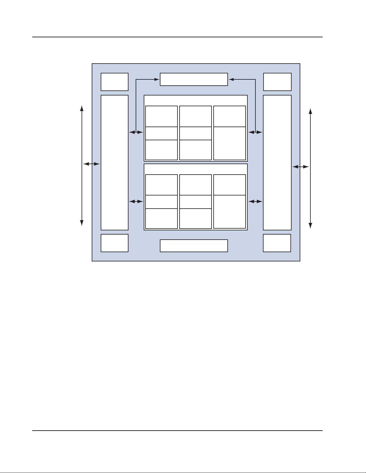
Figure 1: Block Diagram
Primary PCI/PCI-X Bus
Secondary PCI/PCI-X Bus
80B6000_BK001_02
JTAG
Secondary
Bus Arbiter
Primary
Clock PLL
Secondary
Clock PLL
PCI-X
Interface
Bus
Master
Bus
Slave
PCI-X
Interface
Configuration Registers
Clocking & Reset
Data/Control Unit
Queue
Compare
Logic
Read Queue
8 entries
PW Queue
8 entries
Address
Decode
Control
Logic
Burst Read
Buffer
4 Kbytes
Posted Write
Buffer
1 Kbyte
Single Data
Phase Buffer
4 Bytes
Data/Control Unit
Queue
Compare
Logic
Read Queue
8 entries
PW Queue
8 entries
Address
Decode
Control
Logic
Burst Read
Buffer
4 Kbytes
Posted Write
Buffer
1 Kbyte
Single Data
Phase Buffer
4 Bytes
Bus
Slave
Bus
Master
1. Functional Overview20
Tsi310 User Manual
80B6020_MA001_05
The Tsi310 is composed of the following major functional blocks (see Figure 1):
• The device has two PCI-X interfaces. Each interface handles the PCI/PCI-X protocol for its
respective bus and depending on the type of transaction, can act as either a bus master or a
bus slave. These interfaces transfer data and control information flowing to and from the
blocks shown in the middle of the diagram.
• Two phase-locked loops (PLLs), one for the primary clock domain and one for the
secondary clock domain. The PLL for each clock domain is used when that bus is running
in PCI-X mode; in PCI mode, the PLL is bypassed to allow the full frequency range as
defined by the bus architecture. The two bus clocks may be run synchronously or
asynchronously. A spread-spectrum clock input, within the architectural bounds, is
supported for either or both interfaces.
• One set of configuration registers, programmable either from the primary or secondary
interface. The first 64 bytes of this address space conform to the architectural format for
bridge devices, called Header Type 1. The remaining 192 bytes are device-specific
registers. Each register is fully defined in Section 5.1.2 on page 64.
Page 21

1. Functional Overview 21
• T wo data/control units, one for downstream transactions and one for upstream transactions.
These symmetric units each contain separate buffers for burst read, posted write, and single
data phase operations. Read and write queues, queue compare logic, address decoding,
control logic, and other control functions are also included in these blocks.
• An arbiter for the secondary bus, which can be disabled if an external arbiter is employed.
When enabled, bus arbitration is provided for the Tsi310 and up to six other masters. Each
client can be assigned high or low priority, or can be masked off.
• A clocking and reset control unit to manage these common device functions.
• A JTAG controller, compliant with IEEE Standard 1149.1, to facilitate boundary scan
testing.
Tsi310 User Manual
80B6020_MA001_05
Page 22

1.2 Features
The Tsi310 has the following key features:
1.2.1 PCI-X Interfaces
• Complies with the following specifications:
— PCI Local Bus Specification (Revision 2.2)
— PCI-to-PCI Bridge Architecture Specification (Revision 2.0)
— PCI-X Addendum to PCI Local Bus Specification (Revision 1.0a)
• Uses the 3.3V signaling environment and does not support the optional 5 V I/O signaling
levels
• Primary and secondary interface clocks may be run synchronously or asynchronously
• Concurrent primary and secondary bus operations
• Supports configurations of PCI mode or PCI-X mode on either bus in any combination
1. Functional Overview22
1.2.2 Memory Buffer Architecture
• 4KB of buffering for upstream memory burst read commands, with up to eight active
transactions allowed
• 4KB of buffering for downstream memory burst read commands, with up to eight active
transactions allowed
• 1KB of buffering for upstream posted memory write commands, with up to eight active
transactions allowed
• 1KB of buffering for downstream posted memory write commands, with up to eight active
transactions allowed
• Allows one active single data phase (4-byte) delayed or split transaction in each direction
1.2.3 Power Management
• Supports D0 and D3 power states
Tsi310 User Manual
80B6020_MA001_05
Page 23

1. Functional Overview 23
1.2.4 T ransaction Forwarding
• I/O, Memory, and Prefetchable Memory base and limit registers for downstream
forwarding
• Inverse address decoding for upstream forwarding
• Flat addressing model
• Supports VGA-compatible addressing and palette snooping for upstream transactions
• Supports full 64-bit addressing and Dual Address Cycles
• Responds as medium-speed device on both interfaces
1.2.5 Configuration Registers
• 1 set of standard PCI and device specific configuration registers, accessible from both the
primary and secondary interfaces
• Supports Type 0 and Type 1 configuration cycles
1.2.6 Optional Features
• Capable of defining an optional opaque (undecoded) memory address region to facilitate
applications with embedded processors
• Supports secondary side PCI-X device privatization
• Optional Definable Base Address Register for use by embedded sub-systems on the
secondary bus
• Optional access to configuration register space from the secondary bus
1.2.7 Bus Arbitration
• On-chip programmable bus arbiter for the secondary bus with support for up to six external
masters
• Priority and masking control for each agent
1.2.8 IEEE® 1149.1 JTAG Port
• Performs boundary-scan testing
Tsi310 User Manual
80B6020_MA001_05
Page 24

1.3 Operation Overview
This section briefly describes the operation of various aspects of the Tsi310. For more
information on each topic, refer to subsequent chapters.
1.3.1 Supported Modes
The Tsi310 is a full-function transparent PCI-X to PCI-X bridge. As such, either interface may
be configured to operate using the conventional PCI bus protocol or the PCI-X bus protocol. In
mixed-mode configurations, the Tsi310 hardware handles the conversion from one protocol to
the other.
Any allowed bus clock frequency range for a particular mode may be used: up to 66 MHz for
PCI mode, and up to 133 MHz for PCI-X mode. Operation at a particular speed depends on the
bus topology and loading. Since the two clock domains are asynchronous and independent, a
different bus speed may be used on each interface. Speed-matching is accomplished using the
buffering structure of the Tsi310 design.
The Tsi310 implements a 64-bit bus on both interfaces. The PCI architecture also allows either
side to be connected to a 32-bit bus or to 32-bit devices. Full 64-bit addressing capability is also
provided, including support for dual address cycles (DAC).
1. Functional Overview24
The Tsi310 uses the 3.3V signaling environment and is not tolerant of 5V signal
levels. When the Tsi310 is mounted on an adapter card, the card must use the 3.3V
connector keying scheme.
1.3.2 Buffer Structure
The Tsi310 contains two symmetric sets of buffers with associated queues, one for upstream
transactions and the other for downstream transactions.
1.3.2.1 Burst Read Buffers
Each burst read buffer shown in Figure 1 on page 20 contains 4 KB to hold data from memory
burst read transactions. Each buffer is logically divided into eight independent 512 -by te bu ffers
to allow for multi-threading. Each 512-byte buffer has a read queue providing up to eight active
read transactions in each direction.
Tsi310 User Manual
80B6020_MA001_05
Page 25

1. Functional Overview 25
Every 512-byte buffer is further divided into four 128-byte subsections. Activity generally
occurs on these 128-byte boundaries. Filling and/or emptying 128 bytes causes bus transactions
to be initiated. While each read queue entry has up to 512 bytes of buffer space associated with
it, to keep data flowing efficiently the 128-byte subsections are re-used as needed when they are
emptied. This means that when the primary and secondary interfaces are running at similar
frequencies and there is little bus contention, long transfers can proceed without disconnection,
after the initial latency needed to fill the first 128-byte subsection. For large transfers when the
two buses are running at vastly dissimilar frequencies, disconnections may occur on the faster
bus as often as every 128 bytes as the 512-byte buffer becomes completely full or empty.
1.3.2.2 Posted Write Buffers
The posted write buffers each have a capacity of 1 KB to hold data from posted memory write
transactions. Each is logically divided into eight independent 128-byte segments to allow
transactions to be issued on the destination bus before they have been completed on the
originating bus. Unlike the burst read buffers, the amount of space assigned to each transaction
is dynamic. A single transaction can utilize from one to eight 128-byte subsections as needed.
Each posted write queue is an 8-entry FIFO, providing up to eight active write transactions in
each direction. Activity generally occurs when a 128-byte segment is filled or emptied, this
keeps data flowing by re-using 128-byte subsections as they become available.
1.3.2.3 Single Data Phase Buffers
There is one single data phase buffer for each direction to hold read or write data from 4-byte
split or delayed transactions. These transactions include all I/O or configuration operations as
well as doubleword memory read operations.
1.3.3 Address Decoding
The Tsi310 is a transparent bridge that uses a flat addressing model. Both the PCI and PCI-X
address spaces are split between the primary bus and the secondary bus. Address ranges residing
on the secondary bus are defined by the I/O, memory, prefetchable memory base and limit, and
the optional base address registers 0 and 1 in the bridge configuration space. All other addresses
are assumed to reside on the primary bus. Inverse address decoding determines when to forward
transactions upstream. The only exception is when the optional opaque address range is enabled
and defined by T si310’s base and limit registers. The T si310 does not recognize transactions for
addresses within the opaque range on either bus. This region may be used, for example, for
peer-to-peer communication between devices on the secondary bus.
The Tsi310 supports full 64-bit addressing and handles dual address cycles on both interfaces.
The device provides no capability for translating addresses.
Tsi310’s configuration registers are accessible from either the primary or secondary interface
using T ype 0 configuration read s and writes. On the secondary interface, the bridge claims Type
1 configuration write transactions that specify conversion to a special cycle on an upstream bus
segment.
Tsi310 User Manual
80B6020_MA001_05
Page 26

1.3.4 Bus Arbitration
The T si310 contains an arbiter for the secondary interface that is enabled or disabled through an
input signal pin. It provides bus arbitration for up to six additional masters, each of which may
be assigned high or low priority or may be masked off. When the internal arbiter is used and the
Tsi310 request is not masked off, the bus is parked at the bridge whenever there are no pending
requests.
The arbiter implements a two-level fairness algorithm that allows each device within a level to
receive grant requests cyclically. The arbiter uses the arbitration priority register to determine
which agents are high priority (HP) devices and which are low priority (LP) devices. At
different points in time, snapshots are taken of all pending requests for each priority level. All
captured HP requests are serviced first, then one of the captured LP requests is serviced. At this
point, a new HP snapshot is taken, picking up any new HP requests. All captured HP requests
are serviced before continuing with the next LP request still pending from the previous LP
snapshot. A new snapshot of pending LP requests is taken only after all requests from the
previous LP snapshot have been serviced.
1. Functional Overview26
1.4 Technology Highlights
The Tsi310 is implemented using a 0.25 micron (m) lithography process with a 0.18 m
L
effective
3.3 V to power the device I/O circuits. The device is packaged in a 31mm thermally and
electrically enhanced plastic ball grid array (HPBGA) with 304 balls. For more information, see
Section 8 on page 191 and Section 9 on page 197.
. The device requires two power supplies, one at 2.5 V for internal logic and the other at
Tsi310 User Manual
80B6020_MA001_05
Page 27

2. Bus Operation
This chapter discusses the following topics:
• “Overview of Bus Operation” on page 27
• “Write Transactions” on page 30
• “Read Transactions” on page 33
• “Configuration Transactions ” on page 37
2.1 Overview of Bus Operation
This chapter presents a summary of the PCI and PCI-X transactions, transaction forwarding
across the Tsi310, and transaction termination.
27
Tsi310 User Manual
80B6020_MA001_05
Page 28

2.1.1 Types of Transactions
Tables 1 and 2 list the command code and name for each PCI and PCI-X transaction. For each
transaction type, the middle two columns indicate whether the T si310 can initiate the transaction
as a master on the primary bus and on the secondary bus. The last two columns indicate whether
the bridge responds to the transaction as a target on the primary bus and on the secondary bus.
Table 1: PCI Transactions
Initiates as Master Responds as Target
Command
Code
0000 Interrupt Acknowledge No No No No
0001 Special Cycle Yes Yes No No
0010 I/O Read Yes Yes Yes Yes
0011 I/O Write Yes Yes Yes Yes
0100 Reserved No No No No
T ype of Transaction
Primary Secondary Primary Secondary
2. Bus Operation28
0101 Reserved No No No No
0110 Memory Read Yes Yes Yes Yes
0111 Memory Write Yes Yes Yes Yes
1000 Reserved No No No No
1001 Reserved No No No No
1010 Configuration Read No Yes Yes Type 0
1011 Configuration Write Type 1 Yes Yes Yes
1100 Memory Read Multiple Yes Yes Yes Yes
1101 Dual Address Cycle Yes Yes Yes Yes
1110 Memory Read Line Yes Yes Yes Yes
1111 Memory Wr ite and Invalidate No No Yes Yes
Tsi310 User Manual
80B6020_MA001_05
Page 29

2. Bus Operation 29
Table 2: PCI-X Transactions
Initiates as Master Responds as Target
Command
Code
0000 Interrupt Acknowledge No No No No
0001 Special Cycle Yes Yes No No
0010 I/O Read Yes Yes Yes Yes
0011 I/O Write Yes Yes Yes Yes
0100 Reserved No No No No
0101 Reserved No No No No
0110 Memory Read Yes Yes Yes Yes
0111 Memory Write Yes Yes Yes Yes
1000 Alias to Memory Read Block No No Yes Yes
Type of Transaction
Primary Secondary Primary Secondary
1001 Alias to Memory Write Block No No Yes Yes
1010 Configuration Read No Yes Yes Type 0
1011 Configuration Write Type 1 Yes Yes Yes
1100 Split Completion Yes Yes Yes Yes
1101 Dual Address Cycle Yes Yes Yes Yes
1110 Memory Read Block Yes Yes Yes Yes
1111 Memory Wr ite Block Yes Yes Yes Yes
As indicated in the previous tables, certain commands are not supported by the Tsi310:
• The bridge never initiates a transaction with a reserved command code and, as a target, the
bridge ignores reserved command codes.
• The bridge never initiates an interrupt acknowledge transaction and, as a target, the bridge
ignores interrupt acknowledge transactions. Interrupt acknowledge transactions are
expected to reside entirely on the primary bus closest to the host bridge.
• The bridge does not respond to special cycle transactions. To generate special cycle
transactions on other buses, either upstream or downstream, a Type 1 configuration
command must be used.
• The Tsi310’s response to Type 1 Configuration accesses on the secondary interface is
limited. The Tsi310 only responds to Type 1 configuration writes that get converted to
special cycles going upstream, as described in Section 2.4.4 on page 42.
Tsi310 User Manual
80B6020_MA001_05
Page 30

• The Tsi310 does not generate Type 0 configuration transactions on the primary interface.
• The T si310 never initiates a Memory Write and Invalidate command on either interface. As
a target, the bridge will accept a Memory Write and Invalidate command and forward it to
the destination interface as a Memory Write command.
2.2 Write Transactions
Write transactions are treated as either posted, delayed/split (PCI-X), or immediate write
transactions, as shown in the following table.
Table 3: Write Transaction Handling
Type of Transaction Type of Handling
Memory Write Posted
Memory Write and Invalidate Posted
Memory Write Block (PCI-X) Posted
2. Bus Operation30
I/O Write Delayed/Split (PCI-X)
Type 0 Configuration Write Immediate on the primary bus, Delayed/Split
Type 1 Configuration Write Delayed/Split (PCI-X)
2.2.1 Posted Write Transactions
The posted mode is the default mode used for the memory-write and
memory-write-and-invalidate transactions. The memory-write-block transaction also uses the
posted mode. Posted is the only mode used for the memory-write-block command.
When the Tsi310 determines that a memory write transaction is to be forwarded across the
bridge, it first checks for empty space in the posted write buffer. If space is available in the
posted write buffer, the Tsi310 accepts data until the buffer is full or the transaction is
terminated. If the transaction is terminated because the buffer is full, the transaction is
terminated on a 128-byte boundary. If there is no space in the posted write buffer , the transaction
is terminated with retry.
Up to eight posted write transactions can be enqueued in the Tsi310.
(PCI-X) on the secondary bus.
Tsi310 User Manual
80B6020_MA001_05
Page 31

2. Bus Operation 31
2.2.1.1 PCI to PCI-X Transactions
When the originating bus is operating in the conventional PCI mode and the destination bus is
operating in PCI-X mode, the Tsi310 must buffer memory write transactions from the
conventional PCI interface and count the number of bytes to be forwarded to the PCI-X
interface. If the conventional PCI transaction uses the memory write command and some byte
enables are not asserted, the Tsi310 must use the PCI-X memory write command. If the
conventional PCI command is memory write and all byte enables are asserted, the bridge will
use the memory write PCI-X command. If the conventional transaction uses the memory write
and invalidate command, the bridge uses the PCI-X memory write block command.
The Tsi310 attempts to transfer the write data on the PCI-X interface as soon as the transaction
ends or a 128-byte boundary is crossed, whichever comes first. Writes of greater than 128 bytes
are possible only if more than one 128-byte sector fills up before the write operation is issued on
the PCI-X interface.
2.2.1.2 PCI-X to PCI Transactions
When the originating bus is operating in PCI-X mode and the destination bus is operating in the
conventional PCI mode, the Tsi310 uses the conventional memory write command for both the
PCI-X memory write and PCI-X memory write block commands.
The Tsi310 attempts to transfer write data on the conventional PCI interface when the PCI-X
data crosses a 128-byte boundary or the end of the PCI-X transfer occurs, whichever comes
first. As long as a 128-byte buffer is full, or the end of transfer remains from the PCI-X memory
write command when a 128-byte boundary is crossed, the transfer will continue on the
conventional PCI interface.
2.2.1.3 PCI to PCI Transactions
When both buses are operating in conventional PCI mode, the Tsi310 passes a memory write
command that it receives to the destination interface. However, if command received is a
memory write and invalidate command, the T si310 will forward it on to the destination interface
as a memory write command.
The Tsi310 attempts to transfer a memory write command when the transaction ends or a
128-byte boundary is crossed, whichever comes first. As long as a 128-byte buffer is full or the
end of transfer remains from the PCI memory write command when a 128-byte boundary is
crossed, the transfer will continue.
Tsi310 User Manual
80B6020_MA001_05
Page 32

2.2.1.4 PCI-X to PCI-X Transactions
When both buses are operating in PCI-X mode, the Tsi310 passes the memory write command
that it receives to the destination interface along with the originating byte count and transaction
ID.
The Tsi310 attempts to transfer a memory write command when the transaction ends or a
128-byte boundary is crossed, whichever comes first. As long as a 128-byte buffer is full or the
end of transfer remains from the PCI-X memory write command when a 128-byte boundary is
crossed, the transfer will continue.
If a transaction is disconnected on the destination interface in the middle of a continuing
transfer, the byte count and address are updated and the transaction is presented again on the
destination interface. If a transaction is disconnected in the middle of a continuing transfer on
the originating interface, the originator must present the transaction again with the updated byte
count and address.
2.2.2 Delayed/Split Write Transactions
I/O writes, Type 1 configuration writes, and Type 0 configuration writes on the secondary bus
are treated as delayed transactions by the T si310. These commands are retried on the originating
bus, completed on the destination bus if necessary, and then completed on the originating bus.
The Tsi310 executes DWord transactions only as delayed transactions in the conventional PCI
mode and as split requests in PCI-X mode.
2. Bus Operation32
There is only one request queue entry for either delayed or split write transactions.
2.2.3 Immediate Write Transactions
Type 0 configuration writes on the primary PCI interface meant for the Tsi310 are treated as an
immediate write transaction by the bridge. The Tsi310 executes the transaction and indicates its
completion by accepting the DWord of data immediately.
Tsi310 User Manual
80B6020_MA001_05
Page 33

2. Bus Operation 33
2.3 Read Transactions
Read transactions are treated as either delayed (PCI), split (PCI-X), or immediate read
transactions, as shown in the following table.
Table 4: Read Transaction Handling
Type of Transaction Type of Handling
Memory Read Delayed
Memory Read Line Delayed
Memory Read Multiple Delayed
Memory Read DWord (PCI-X) Split (PCI-X)
Memory Read Block (PCI-X) Split (PCI-X)
I/O Read Delayed/Split (PCI-X)
Type 0 Configuration Read Immediate on the primary bus, Delayed/Split
(PCI-X) on the secondary bus
Type 1 Configuration Read Delayed/Split (PCI-X)
2.3.1 Memory Read Transactions
The conventional PCI memory-read, memory-read-line, memory-read-multiple, PCI-X
memory-read-DWord, and PCI-X memory-read-block transactions are used to transfer memory
data from the originating side of the Tsi310 to the destination side. All memory read
transactions are either delayed or split on the originating interface depending on the mode of the
originating interface.
2.3.1.1 PCI to PCI-X Transactions
The Tsi310 must translate the conventional memory read command to either the memory read
DW ord or the memory read block PCI-X Command. If the conventional memory read command
targets non-prefetchable memory space, the command is translated into a memory read DWord.
In any other instance the conventional memory read command gets translated into a memory
read block PCI-X command. The prefetching algorithm for the conventional memory read
command in the prefetchable space is controlled by bits 9:8 of the primary and secondary data
buffering control registers. The default value of these bits indicates that one cache line will be
prefetched.
The Tsi310 must translate the conventional memory read line command to the memory read
block PCI-X command. The prefetching algorithm is controlled by bits 7:6 of th e primary and
secondary data buffering control registers. The default value of these bits indicates that one
cache line will be prefetched.
Tsi310 User Manual
80B6020_MA001_05
Page 34

The T si310 must translate the conventional memory read multiple command to the memory read
block PCI-X command. The prefetching algorithm is controlled by bits 5:4 of th e primary and
secondary data buffering control registers. The default value of these bits indicates that a full
prefetch will be done, subject to the limit imposed by the maximum memory read byte count
value set by bits (14:12) of the same register. The default value for this field is 512 bytes or an
entire read buffer. Using a value greater than this is possible, but it may be constrained by the
setting of the split transaction commitment limit value in the upstream or downstream split
transaction register, since the target bus is in PCI-X mode (or more information about these
registers, see Section 5.5.21 on page 140 and Section 5.5.22 on page 141, respectively). Data
fetching operations will be disconnected at all 1MB boundaries.
2.3.1.2 PCI-X to PCI Transactions
The Tsi310 translates PCI-X memory read DWord commands into conventional memory read
commands.
The T si310 translates a PCI-X memory read block command into one of three conventional PCI
memory read commands based on the byte count and starting address. If the starting address and
byte count are such that only a single DWord (or less) is being read, the conventional transaction
uses the memory read command. If the PCI-X transaction reads more than one DWord, but does
not cross a cache line boundary (as indicated by the Cache Line Size register in the conventional
Configuration Space header), the conventional transaction uses the memory read line command.
If the PCI-X transaction crosses a cache line boundary, the conventional transaction uses the
memory read multiple command.
2. Bus Operation34
If a disconnect occurs before the byte count of the PCI-X memory read block command is
exhausted, the bridge continues to issue the command until all the bytes in the count are
received. The bridge disconnects once the buffer is filled and prefetches more data as 128-byte
sectors of the buffer become free when split completion data is returned to the originator, until
the byte count is exhausted.
2.3.1.3 PCI to PCI Transactions
This mode does not involve any translation.
If the memory read command targets non-prefetchable memory space, the memory read fetches
only the requested double word. Bits 9:8 of the primary and secondary data buffering control
registers control the prefetching algorithm for the memory read command in prefetchable space.
The default value of these bits indicates that up to one cache line will be prefetched.
For the memory read line command, the prefetching algorithm is controlled by bits 7:6 of the
primary and secondary data buffering control registers. The default value of these bits indicates
that up to one cache line will be prefetched.
Tsi310 User Manual
80B6020_MA001_05
Page 35

2. Bus Operation 35
For the memory read multiple command, the prefetching algorithm is controlled by bits 5:4 of
the primary and secondary data buffering control registers. The default value of these bits
indicates that a full prefetch will be done, subject to the limit imposed by the maximum memory
read byte count value set by bits (14:12) of the same register. The default value is 512 bytes or
an entire read buffer. Data fetching operations will be disconnected at all 1 MB boundaries.
2.3.1.4 PCI-X to PCI-X Transactions
This mode does not involve any translation.
The amount of data that is fetched is controlled by the downstream and upstream split
transaction control register. The split transaction capacity and split transaction commitment
limit fields control how much data is requested at any one time (for more information, see
Section 5.5.21 on page 140 and Section 5.5.22 on page 141).
2.3.2 I/O Read
The I/O Read command is not translated and fetches a DWord of data. The command will either
be split in the PCI-X mode or delayed in the conventional PCI mode.
2.3.3 Configuration Read
2.3.3.1 Type 1 Configuration Read
The Type 1 configuration read command is only accepted on the primary interface. The
command will either be split in PCI-X mode or delayed in the conventional PCI mode.
2.3.3.2 Type 0 Configuration Read
The Type 0 configuration read command is accepted on either the primary or secondary
interface. The command returns immediate data on the primary interface regardless of the
interface mode. On the secondary interface the command is treated as a delayed transaction in
PCI mode, and as a split transaction in PCI-X mode.
2.3.4 Non-Prefetchable and DWord Reads
A non-prefetchable read transaction is a read transaction in which the Tsi310 requests exactly
one DWord from the target and disconnects the initiator after delivering that one DWord of read
data. Unlike prefetchable read transactions, the Tsi310 forwards the read byte enable
information for the data phase.
Non-prefetchable behavior is used for I/O, configuration, memory read transactions that fall into
the non-prefetchable memory space for PCI mode, and all DWord read transactions in PCI-X
mode.
Tsi310 User Manual
80B6020_MA001_05
Page 36

2.3.5 Prefetchable Reads
A prefetchable read transaction is a read transaction where the Tsi310 performs speculative
reads, transferring data from the target before it is requested from the initiator. This behavior
allows a prefetchable read transaction to consist of multiple data transfers. For prefetchable read
transactions, all byte enables are asserted for all data phases.
Prefetchable behavior is used for memory read line and memory read multiple transactions, as
well as for memory read transactions that fall into prefetchable memory space and are allowed
to fetch more than a DWord. The amount of data that is prefetched depends on the type of
transaction and the setting of bits in the primary and secondary data bufferi ng co ntro l registers
in configuration space. The amount of prefetching may also be affected by the amount of free
buffer space available in the T si310, and by any read address boundaries encountered. Examples
of these boundaries are cache line for cache line reads and 1M address boundary to ensure that a
read does not cross into another devices’ space.
2.3.5.1 Algorithm for PCI-to-PCI Mode
The algorithm used for transfers in PCI-to-PCI mode is user defined in the primary and
secondary data buffering control registers. These registers have bits for memory read to
prefetchable space, memory read line, and memory read multiple transactions. For memory
read, the bits select whether to read a DWord, read to a cache line boundary, or to fill the
prefetch buffer. For memory read line and memory read multiple transactions, the bits select
whether to read to a cache line boundary or to fill the prefetch buffer. In all cases, if the bits are
selected to fill the prefetch buffer, the maximum amount of data that is requested on the target
interface is controllable by the setting of the maximum memory read byte count bits of the
Primary and Secondary Data Buffering Control registers. When more than 512 bytes are
requested, the Tsi310 fetches data to fill the buffer and then fetches more data to keep the buf fer
filled as sectors (128 bytes) are emptied and become free to use again.
2. Bus Operation36
2.3.5.2 Algorithm for PCI-to-PCI-X Mode
The algorithm for transfers in this mode is much the same as for transfers in PCI-to-PCI mode,
except that the maximum request amount may be additionally constrained by the setting of the
split transaction commitment limit value in the upstream or downstream split transaction
register. The only other dif ference is that prefetching will not cease when the originating master
disconnects. Prefetching will only cease when all of the requested data is received, as required
by the PCI-X architecture.
Tsi310 User Manual
80B6020_MA001_05
Page 37

2. Bus Operation 37
2.3.5.3 Algorithm for PCI-X-to-PCI and PCI-X-to-PCI-X Mode
The algorithm for transfers in these modes is to transfer the amount of requested data.
In the PCI-X-to-PCI mode, the Tsi310 continues to generate data requests to the PCI interface
and keeps the prefetch buffer full until the entire amount of data requested is transferred.
In the PCI-X to PCI-X mode, the algorithm is controlled by the split transaction commitment
limit value contained in the upstream or downstream split transaction register. If the value is
greater than or equal to the split transaction capacity (4KB) but less than 32KB, the maximum
request amount is 512 bytes. Larger transfers will be decomposed into a series of smaller
transfers, until the original byte count has been satisfied. If the commitment limit value indicates
32KB or more, the original request amount is used and decomposition is not performed (for
more information, see Section 5.5.21 on page 140 and Section 5.5.22 on page 141).
If the original request is broken into smaller requests the Tsi310 waits until the previous
completion has been totally received before a new request is issued. This ensures that the data
does not get out of order and that two requests with the same sequence ID are not issued. In any
case, the bridge generates a new requester ID for each request passed through the bridge.
2.4 Configuration Transactions
The PCI Local Bus Specification (Revision 2.2) defines two configuration transaction types,
Type 0 and Type 1. These two configuration formats are distinguished by the value of bus
address bits (1:0). If address bits (1:0) are b‘00’ during a configuration transaction, a Type 0
configuration transaction is being indicated. A Type 0 configuration transaction is used to
access configuration information for devices on the current bus segment. A Type 0
configuration transaction is not forwarded across the Tsi310, but rather is used to configure the
bridge itself. If address bits (1:0) are b‘01’ during a configuration transaction, a Type 1
configuration transaction is being indicated. T ype 1 configuration transactions are used to access
devices that reside behind one or more bridges.
Figure 2 shows the address formats for Type 0 and Type 1 configuration transactions.
The register number is found in both T ype 0 and Type 1 formats and gives the DW ord address of
the configuration register to be accessed. The function number is also included in both formats
and indicates which function of a multi-function device is to be accessed. For single-function
devices, this value is not decoded. Configuration transaction addresses for Type 1 and PCI-X
T ype 0 formats also include a 5-bit field designating the device number that identifies the device
on the target PCI bus that is to be accessed. This device number is decoded to determine which
IDSEL signal is asserted for the transaction. Finally, Type 1 transactions also include a bus
number field that is used by the T si310 to determine where in the bus hierarchy the transaction is
targeted.
Tsi310 User Manual
80B6020_MA001_05
Page 38

Figure 2: Configuration Transaction Address Formats
31 027811 10
Reserved
Function
Register Number 0 1
1
PCI Type 1
Device NumberBus Number
15162324
Number
AD(31:0)
31
027811 10
Function
Register Number 0 0
1
PCI Type 0
See PCI 2.2 Specification and table below
Number
AD(31:0)
31 027811 10
Reserved
Function
Register Number 0 1
1
PCI-X Type 1
Device NumberBus Number
15162324
Number
AD(31:0)
31
027811 10
Function
Register Number 0 0
1
PCI-X Type 0
See PCI-X Addendum and table below
Number
AD(31:0)
16 15
Device Number
2. Bus Operation38
2.4.1 Configuration Type 0 Access to Bridge
The configuration space of the Tsi310 is accessed by Type 0 configuration transactions. The
configuration space of the bridge can be accessed from either the primary bus or the secondary
bus. Applications which do not require access from the secondary bus should tie down the
S_IDSEL pin.
On the primary bus, the Tsi310 responds to a Type 0 configuration transaction by accepting the
transaction when the following conditions are met during the address phase:
• P_C/BE(3:0)# command indicates a configuration read or configuration write transaction
• P_AD(1:0) are b'00'
• P_IDSEL is asserted
• Bit 2 of the Miscellaneous Control Register must be set to b‘0’
Tsi310 User Manual
80B6020_MA001_05
Page 39

2. Bus Operation 39
On the secondary bus, the Tsi310 responds to a Type 0 configuration transaction by accepting
the transaction when the following conditions are met during the address phase:
• S_C/BE(3:0)# command indicates a configuration read or configuration write transaction
• S_AD(1:0) are b'00'
• S_IDSEL is asserted
• The Bus Master control bit in the Command Register must be set to b‘1’ from the Primary
Interface
The function number is not decoded since the bridge is a single-function device. All
configuration transactions to the bridge are handled as DWord (single data phase) operations.
2.4.1.1 Type 0 Configuration Transaction Limitation
The T si310 has a transaction limitation when its Pr imary interface is configured in PCI-X mode,
and a Configuration write accesses the Tsi310 register space after it is configured by the host
processor through the Primary interface. The host processor is responsible for configuring all
devices on the Primary bus at power-up, and assigns each device a unique “device number.”
This number is defined by AD[15:11] of the address Type 0 configuration write transaction.
Each time a configuration write is initiated to the Tsi310 this device number is updated. The
device number can be read at offset 0x84 of Tsi310’s configuration space (see Section 5.5.20 on
page 137).
The T s i310 contains a feature that allows devices connected to its Secondary interface to access
Tsi310’s registers through Type 0 configuration cycles. For example, when a Type 0
configuration write is initiated to the bridge’s Secondary interface the contents of the Tsi310
device number is updated. Users should be aware, however, that transaction accesses to the
Tsi310 from the Secondary interface could overwrite the bridge’s device number. As a result, it
is possible that two devices may have the same device number.
If a user needs to access the Tsi310 from the Secondary interface after reset (for
example, to set up Opaque regions), IDT recommends completing a configuration
read of offset 0x84 to determine the Tsi310's device number assigned upon initial
configuration. Once the device number is determined it must be included in
AD[15:11] of any configuration write access to the bridge from the Primary or
Secondary interface.
Tsi310 User Manual
80B6020_MA001_05
Page 40

2.4.2 Type 1 to Type 0 Translation by Bridge
Type 1 configuration transactions are used to configure devices in a hierarchical bus structure
having one or more bridges. A bridge is the only type of device that should respond to a Type 1
configuration transaction. T ype 1configuration commands are used to access PCI/PCI-X devices
that are located on a bus segment other than the one where the Type 1 transaction is initiated.
The Tsi310 performs a Type 1 to Type 0 translation when a Type 1 transaction is presented on
the primary interface that is destined for a device attached directly to the secondary interface. In
this case, the bridge must convert the configuration transaction to a Type 0 format so that the
secondary bus device can accept it. Type 1 to Type 0 translations are never performed in the
upstream direction.
The Tsi310 claims a Type 1 configuration transaction on its primary bus and translates it into a
Type 0 transaction on the secondary bus when the following conditions are met during the
address phase:
• P_C/BE(3:0)# command indicates a configuration read or configuration write transaction
• P_AD(1:0) are b‘01’
2. Bus Operation40
• The bus number on P_AD(23:16) is the same as the value in the secondary bus number
register in the bridge’s configuration space
When the Tsi310 translates the Type 1 transaction to a Type 0 transaction on the secondary
interface, it performs the following translations to the address:
• Sets S_AD(1:0) to b‘00’
• Decodes the device number specified and drives the bit pattern specified in Table 5 on
S_AD(31:16) for use in the assertion of the device’s IDSEL signal
• Sets S_AD(15:11) to b‘00000’ if the secondary bus is operating in conventional PCI mode
(in the PCI-X mode, the device number is passed through unchanged)
• Leaves the function number and register number fields unchanged
The Tsi310 asserts a unique address signal based on the device number. These address signals
may be used as secondary bus IDSEL signals. Mapping of the address signals depends on the
device number on P_AD(15:11) of the Type1 configuration transaction.
Table 5 indicates how the bridge decodes the device number field. This default mapping may be
modified by the secondary bus private device mask register (see Section 5.5.29 on page 146.
Tsi310 User Manual
80B6020_MA001_05
Page 41

2. Bus Operation 41
Table 5: IDSEL Generation
Primary Address
Device Number
x’00’ 00000 0000 0000 0000 0001
x’01’ 00001 0000 0000 0000 0010
x’02’ 00010 0000 0000 0000 0100
x’03’ 00011 0000 0000 0000 1000
x’04’ 00100 0000 0000 0001 0000
x’05’ 00101 0000 0000 0010 0000
x’06’ 00110 0000 0000 0100 0000
x’07’ 00111 0000 0000 1000 0000
x’08’ 01000 0000 0001 0000 0000
P_AD(15:11)
Secondary Address S_AD(31:16)
x’09’ 01001 0000 0010 0000 0000
x’0A’ 01010 0000 0100 0000 0000
x’0B’ 01011 0000 1000 0000 0000
x’0C’ 01100 0001 0000 0000 0000
x’0D’ 01101 0010 0000 0000 0000
x’0E’ 01110 0100 0000 0000 0000
x ’0F’ 01111 1000 0000 0000 0000
x’10’ - x’1E’ 10000 - 11110 0000 0000 0000 0000
x’1F’ 11111 0000 0000 0000 0000
or may convert to a special cycle
transaction if all criteria are met (see
Section 2.4.4 on page 42)
The Tsi310 forwards Type 1 to Type 0 configuration read or configuration write transactions as
delayed transactions in PCI mode, or as split transactions in PCI-X mode.
Tsi310 User Manual
80B6020_MA001_05
Page 42

2.4.3 Type 1 to Type 1 Forwarding by Bridge
Type 1 to Type 1 transaction forwarding provides a means to configure devices when a
hierarchical bus structure containing two or more levels of bridges is used.
When the Tsi310 accepts a Type 1 configuration transaction destined for a PCI/PCI-X bus
downstream from its secondary interface, the bridge forwards the transaction unchanged to the
secondary bus. Eventually, this transaction is translated to a Type 0 configuration transaction or
to a special cycle transaction by a downstream bridge.
Downstream T ype 1 to Type 1 forwarding occurs when the following conditions are met during
the address phase:
• P_C/BE(3:0)# command indicates a configuration read or configuration write transaction
• P_AD(1:0) are equal to b‘01’
• the specified bus number is within the range defined by the secondary bus number register
(exclusive) and the subordinate bus number register (inclusive)
The Tsi310 also supports Type 1 to Type 1 forwarding of configuration write transactions
upstream to allow for the generation of upstream special cycle transactions, as described in
Section 2.4.4 on page 42. All upstream Type 1 configuration read transactions are ignored by
the bridge.
2. Bus Operation42
The Tsi310 forwards Type 1 to Type 1 configuration read and configuration write transactions
as delayed transactions in PCI mode, and as split transactions in PCI-X mode.
2.4.4 Special Cycle Generation by the Bridge
The Type 1 configuration transaction format may be used to generate special cycle transactions
in hierarchical PCI/PCI-X systems. Special cycle transactions can be generated from Type 1
configuration write transactions in either the upstream or the downstream direction.
The Tsi310 initiates a special cycle on the destination bus when a Type 1 configuration write
transaction is detected on the initiating bus and the following conditions are met during the
address phase:
• The command is a configuration write
• Address bits AD(1:0) are b‘01’
• The device number in address bits AD(15:11) is equal to b‘11111’
• The function number in address bits AD(10:8) is equal to b‘111’
• The register number in address bits AD(7:2) is equal to b‘000000’
• The specified bus number is the same as the value in Tsi310’s secondary bus number
register (for downstream transactions) or matches the value in its primary bus number
register (for upstream transactions)
Tsi310 User Manual
80B6020_MA001_05
Page 43

2. Bus Operation 43
When the Tsi310 initiates the transaction on the destination interface, the command is changed
from a configuration write to a special cycle. Devices that use special cycles ignore the address
and decode only the bus command. The data phase contains the special cycle message. The
transaction is forwarded as a delayed transaction in PCI mode and as a split transaction in PCI-X
mode. Once the transaction is completed on the destination bus through the detection of the
master abort condition, the Tsi310 completes the transaction on the originating bus by accepting
the retry of the delayed command in PCI mode, or by generating a completion message in
PCI-X mode.
Special cycle transactions received by the Tsi310 as a target are ignored.
Tsi310 User Manual
80B6020_MA001_05
Page 44

2. Bus Operation44
Tsi310 User Manual
80B6020_MA001_05
Page 45

3. Clocking and Reset Options
This chapter discusses the following topics:
• “Clocking Domains” on page 45
• “Clock Jitter” on page 46
• “Mode and Clock Frequency Determination” on page 46
• “Clock Stability” on page 48
• “Driver Impedance Selection” on page 49
• “Reset Functions and Operations” on page 50
• “Bus Parking and Bus Width Determination” on page 53
• “Power Management and Hot-Plug” on page 54
• “Secondary Device Masking” on page 55
• “Handling of Address Phase Parity Errors” on page 55
45
• “Optional Base Address Register” on page 55
• “Optional Configuration Register Access from the Secondary Bus” on page 56
• “Short Term Caching” on page 57
3.1 Clocking Domains
The Tsi310 has two clocking domains, one for the primary interface and one for the secondary
interface. Each interface has its own clock input pin. The primary interface is controlled by the
P_CLK input. The secondary interface and the internal arbiter are controlled by the S_CLK
input. The T si310 does not supply the clocks on either interface. The two bus clocks may be run
synchronously or asynchronously to one another. The two clock frequencies are independent of
each other and each may have any value allowed by the PCI/PCI-X bus architectures. A spread
spectrum clock input is supported for either or both interfaces within the architectural bounds.
The Tsi310 contains a separate internal phase-locked loop (PLL) circuit for each clocking
domain. The PLL for each interface is employed when its bus is running in PCI-X mode, as
determined by the bus initialization process described below . When either bus is running i n PCI
mode, the respective PLL is bypassed to allow for any clock frequency from zero to 66 MHz.
Tsi310 User Manual
80B6020_MA001_05
Page 46

3.2 Clock Jitter
Clock jitter is defined as the relationship of one clock edge to a subsequent clock edge,
measured at the same point. If these two edges are separated by one clock cycle, it is called
cycle-to-cycle or short-term jitter. If they are separated by hundreds or thousands of cycles, it is
called long-term jitter. As specified in Section 8 on page 191, the Tsi310 tolerates a maximum
of ± 250 ps of short-term and long-term jitter on each of its clock inputs. Clock jitter introduced
by the internal PLLs of the bridge is accounted for within this maximum specification.
Careful design of the clock generation circuitry is an important factor in determining the speed
of the bus. As indicated in the PCI and PCI-X architectures, all sources of clock jitter must be
considered when determining the bus clock frequency. The minimum and maximum clock
period specifications must not be violated for any single clock cycle. The system clock output
period, including all sources of clock period variation such as jitter and component tolerances,
must always be within the minimum and maximum limits defined for the mode in which the bus
is configured. For example, if a specific system clock design has a maximum clock period
variation of 180 ps, then the nominal clock period for the PCI-X 133 range needs to be at least
7.68ns (7.5ns + 0.180ns), making the maximum frequency allowed for this case is just over 130
MHz.
3. Clocking and Reset Options46
3.3 Mode and Clock Frequency Determination
As explained in Sections 6.2 and 8.9 of the PCI-X Addendum to PCI Local Bus Specification
(Revision 1.0a), the mode and frequency range of each bus is determined by the values on its
M66EN and PCIXCAP signals when the bus reset signal is active. Each bus client is then
informed of the determination through an initialization pattern that is broadcast at the
de-assertion or rising edge of the reset signal. This process is accomplished on the secondary
interface differently than on the primary interface, due to architectural requirements for PCI-X
bridges. The differences for each interface are discussed in the following sections.
3.3.1 Primary Interface
The primary interface is capable of operating in either the conventional PCI mode or in PCI-X
mode, at any of the defined frequency ranges. When the Tsi310 is used on an add-in card, the
M66EN and PCIXCAP pins on the card edge connector should be left unconnected (except for a
required decoupling capacitor to provide an AC return path) to indicate this maximum
capability. As defined by Section 9.10 of the PCI-X Addendum to PCI Local Bus Specification
(Revision 1.0a), an add-in card’s PCIXCAP pin must be consistent with the 133 MHz Capable
bit in the PCI-X Bridge Status register. When the Tsi310 is used on a motherboard, the system
designer should wire the M66EN and PCIXCAP signal networks to all clients on the bus in the
architected fashion to achieve the desired results.
Tsi310 User Manual
80B6020_MA001_05
Page 47

3. Clocking and Reset Options 47
The T si310 does not have I/O pins for th e M66EN or PCIXCAP signals on its primary interface.
The bridge adjusts its internal configuration (including its internal PLLs, if appropriate) solely
on the basis of the initialization pattern it detects on the signals P_DEVSEL#, P_STOP#, and
P_TRDY# at the rising edge of P_RST#. If the internal PLL is used (the bus is configured in
PCI-X mode), a maximum of 100 s from the rising edge of P_RST# is required to lock the PLL
to the frequency of the clock supplied on the P_CLK input.
3.3.2 Secondary Interface
The secondary interface is also capable of operating in either conventional PCI mode or in
PCI-X mode, at any of the defined frequency ranges. Since the Tsi310 acts as the central
resource for the secondary bus, it controls the mode and frequency determination process. As
recommended by Section 14.2 of the PCI-X Addendum to PCI Local Bus Specification
(Revision 1.0a), the bridge uses a programmable pull-up circuit to accomplish this. Figure 3
shows the programmable pull-up circuit and the structure of the network that is connected to the
S_PCIXCAP input of the bridge. Examples of the connections that are expected when
PCI-X 66, PCI-X 133, and conventional PCI clients are attached to the bus are also shown (for
more information, see the PCI-X Addendum). There are two pull-up resistors in the circuit. The
first is an external weak pull-up whose value of 56kis selected to set the voltage of the
S_PCIXCAP input below its low threshold when a PCI-X 66 client is attached. The second is a
strong pull-up, externally wired between the S_PCIXCAP and S_PCIXCAP_PU pins on the
module. Its value of 1k is selected to set the voltage of the S_PCIXCAP input above its high
threshold when all clients on the bus are only PCI-X 66 capable.
During the mode and frequency determination process, the S_PCIXCAP_PU driver is initially
disabled, effectively removing the strong pull-up resistor from the circuit. The Tsi310 begins by
sampling the value on its S_PCIXCAP input. If it detects a b’0’ value, one or more clients have
either pulled the network to ground (if they are PCI-X 66 capable) or tied it to ground (if they
are only capable of conventional PCI operation). To distinguish between these two cases, the
bridge then enables its S_PCIXCAP_PU driver to put the strong pull-up into the circuit. If, after
a sufficient time, the S_PCIXCAP input remains at a b’0’ value, the network must be tied to
ground by one or more clients, and the bus is initialized to the conventional PCI mode. If the
network can be pulled up, one or more clients are capable of only PCI-X 66 operation (and there
are no conventional PCI devices), so the bus is initialized to PCI-X 66 mode.
If the Tsi310 initially samples a b’1’ value on the S_PCIXCAP input, then all clients on the bus
are capable of PCI-X 133 operation. The bridge then samples the S_SEL100 input to distinguish
between the 66-100 MHz and the 100-133 MHz clock frequency ranges. If it detects a b’1’
value on the S_SEL100 input, the bus is initialized with the PCI-X 100 initialization pattern. If
the value is b’0’, the PCI-X 133 initialization pattern is used. These two ranges allow
adjustment of the clock frequency to account for bus loading conditions.
Tsi310 User Manual
80B6020_MA001_05
Page 48

Figure 3: Programmable Pull-up Circuit
3.3V
3.3V
S_PCIXCAP
S_PCIXCAP_PU
Weak
Pull-up
Strong
Pull-up
For PCI-X
66 MHz Cards
For PCI-X
100/133 MHz Cards
For PCI
Cards
S_SEL100
3.3V
For 100 MHz
For 133 MHz
Enabled During
Bus Capability
Determination
Tsi310
10k 0.01uF 0.01uF
0.01uF
56k
10k
1k
3. Clocking and Reset Options48
Since the internal PLL is bypassed in PCI mode and the S_CLK input is used directly, the
Tsi310 has no need to distinguish between the PCI 66 and PCI 33 modes. Therefore the Tsi310
does not have an I/O pin for the M66EN signal on its secondary interface. This signal should be
routed to all devices on the bus in case the other clients require it.
3.4 Clock Stability
The PCI/PCI-X architectures specify that the bus clock must be stable and running at its
designated frequency for at least 100s prior to the de-assertion of the bus reset signal. As the
Tsi310 does not generate the secondary bus clock but does control the secondary bus reset
signal, it must detect when the S_CLK input has become stable in order to meet this
requirement. The input signal S_CLK_ST ABLE is provided for thi s purpose. During a bus reset,
the bridge waits for the assertion of the S_CLK_STABLE input before executing the mode and
frequency determination sequence described in Section 3.3.2 on page 47.
Tsi310 User Manual
80B6020_MA001_05
Page 49

3. Clocking and Reset Options 49
The Tsi310 is expecting at most one transition on the S_CLK_STABLE input from the not
stable to the stable state. The S_CLK_STABLE input may also be tied-up if the secondary clock
input will always be stable prior to the de-assertion of the primary bus reset signal or the
secondary bus reset bit of the bridge control register (see Section 3.6.2 on page 51).There are
several possibilities for the source of the S_CLK_STABLE input signal. For example: some
clock generation circuits that use phase-locked loops provide a lock indicator that may be used
for this purpose. Care must be taken to assure that the lock indicator does not toggle randomly
while the PLL is locking to the desired frequency before reaching a steady state. Another
possibility is to tie-up the signal, this may be useful for fixed frequency applications with simple
clock generators or oscillators. A third possibility may be to use a ‘power good’ indicator, if the
proper stability assurances can be made. Other ways to provide the S_CLK_STABLE input
signal may also be possible.
The S_CLK_ST ABLE input provides another measure of control for cases where the secondary
bus mode and clock frequency could vary from reset to reset, as in motherboard applications
with pluggable slots. In these applications the external clock generation circuitry will need to
adapt to the changes along with the Tsi310. If the S_CLK_STABLE signal is initially held low
during reset, the bridge will not control the S_PCIXCAP network and the clock generation
circuitry is free to do its own mode and frequency determination sequence. The clock frequency
may be adjusted based on the number of populated slots, determined by the PRSNT pins of the
bus. Once the frequency of the S_CLK input is stable, the clock circuit can assert the
S_CLK_STABLE signal to allow the bridge to complete the reset sequence. The clock
generation circuitry must ensure that the clock frequency it provides falls within the range that
the bridge will determine and broadcast on the initialization pattern. To do this, the clock
generator may need to drive the proper values on the S_SEL100 and S_PCIXCAP inputs, in
addition to controlling the S_CLK_STABLE signal. A mismatch between the broadcast
initialization pattern and the actual operating mode and frequency of the bus is a violation of the
architecture and will cause unpredictable results.
3.5 Driver Impedance Selection
On the Tsi310, the output drivers for the bussed PCI/PCI-X interface signals are capable of two
different output impedances, a 40 ohm output impedance for point-to-point applications and a
20 ohm output impedance for multi-point configurations. The output impedance for the primary
and secondary interfaces is separately controlled. The Tsi310 selects a default impedance value
at the de-assertion of the bus reset on the basis of the bus mode and frequency initialization
pattern which was received on the primary interface or generated on the secondary interface. It
is assumed that if a bus is configured to be in the PCI-X 133 mode, it will be lightly loaded and
therefore have a higher impedance. The drivers are put into point-to-point mode for this case.
For all other PCI-X and all PCI configurations, the bridge assumes that the bus is more heavily
loaded and has a lower impedance, so the drivers are set to multi-point mode.
Tsi310 User Manual
80B6020_MA001_05
Page 50

3. Clocking and Reset Options50
There may be some applications for which these assumptions are inaccurate. For example, a
conventional PCI device may be connected in a point-to-point manner. For exceptions like this,
two control input signals are provided, P_DRVR_MODE for the primary interface and
S_DRVR_MODE for the secondary interface. When these inputs are pulled high, the Tsi310
changes the output impedance of the drivers on their respective interfaces to the opposite state
than was assumed by default (see Table 6).
Table 6: Driver Impedance Selection
Default Driver
Mode
Primary Bus
Mode
Conventional
PCI
PCI-X 66 Multi-point (20) Point-to-point
PCI-X 100 Multi-point (20) Point-to-point
PCI-X 133 Point-to-point
a. Note that the values on these inputs are only valid at reset time; they may not be used to change the driver mode
dynamically, though they may be set differently at each reset if desired to account for changes in bus loading and
mode. Regardless of the driver impedance used, signal analysis should always be done with the actual or expected
bus topology and wiring to verify proper operation. Nets may need to be tuned and series terminations or other
adjustments may be required in order to meet the frequency targets.
(P_DRVR_MODE
=0)
Multi-point (20) Point-to-point
(40)
a
Default Driver
Driver Mode if
P_DRVR_MODE=
1
(40)
(40)
(40)
Multi-point (20) PCI-X 133 Point-to-point
Secondary
Bus Mode
Conventional
PCI
PCI-X 66 Multi-point (20) Point-to-point
PCI-X 100 Multi-point (20) Point-to-point
Mode
(S_DRVR_MODE
=0)
Multi-point (20) Point-to-point
(40)
Driver Mode if
S_DRVR_MODE=
1
(40)
(40)
(40)
Multi-point (20)
3.6 Reset Functions and Operations
Each bus interface has an asynchronous bus reset signal that is used at power-on and other times
to place the Tsi310 into a known state. On the primary interface, the reset signal is an input to
the Tsi310. On the secondary interface, the reset signal is an output driven by the bridge in its
role as the central resource for that bus.
3.6.1 Primary Reset
The bus reset for the primary interface is called P_RST#. It is an input to the Tsi310 and is
controlled by an external upstream central resource. When asserted (see Figure 4 on page 52
and Table 7 on page 53) it forces all bus output signals from the bridge into their benign states
and sets all configuration registers within the Tsi310 to their reset values as defined in
Section 2.4 on page 37. Activating the P_RST# signal also causes the secondary bus reset signal
to be asserted, as required by the PCI and PCI-X specifications.
Tsi310 User Manual
80B6020_MA001_05
Page 51

3. Clocking and Reset Options 51
On the de-assertion or rising edge of the P_RST# signal, the initialization pattern is received off
of the bus and latched into the bridge. If the indication is that the primary bus is operating in
PCI-X mode, an internal PLL sources the clock tree for the primary clock domain. The
appropriate range and tuning bits for the PLL are set according to the indicated frequency range,
and an internal PLL reset signal is deactivated to allow the PLL to begin locking to the P_CLK
input frequency. Since the PLL requires an allowance of 100 s to accomplish this frequency
lock, an internal reset is held on the logic in the primary clock domain until this time period has
elapsed. While the internal logic reset is active, the bridge will not respond to any primary bus
transactions. When the primary bus is operating in PCI mode, the internal PLL for the primary
interface is not used. In this case, the internal PLL reset remains activated, keeping the PLL in
the bypass mode, and the internal logic reset is held for only seven additional primary clock
cycles after the rising edge of P_RST#.
3.6.2 Secondary Reset
The bus reset for the secondary interface is called S_RST#, it is an output from the Tsi310.
Whenever P_RST# is asserted or when the secondary bus reset bit (bit 6) of the bridge control
register is set to b’1’, S_RST# is asserted immediately, asychronously to the secondary bus
clock. When the secondary bus reset bit is being used to control S_RST#, the software must be
sure that the required minimum reset active time (T
) of 1 ms is met.
rst
Several things must occur at or prior to the de-assertion of the secondary bus reset signal. Once
P_RST# is de-asserted or the secondary bus reset bit is changed from b’1’ to b’0’, indicating
that S_RST# should be deactivated, the Tsi310 will wait for the S_CLK_STABLE signal to be
asserted before proceeding. The S_CLK input must be stable at a frequency within the bus
capability limits prior to the assertion of S_CLK_STABLE. Since the PCI Local Bus
Specification (Revision 2.2) requires that the bus clock be stable for at least 100 s prior to the
de-assertion of the bus reset, S_CLK_STABLE serves as a gate to a timer that ensures that this
requirement is met. During this time delay period, the determination of the secondary bus mode
and frequency capability is made through the use of the programmable pull-up circuit described
in Section 3.3.2 on page 47. This process may include up to 80 s for the capacitive load on the
S_PCIXCAP net to be charged, making it prudent to overlap the two functions. By the time the
100 s timer expires, the bus capability will have been determined and the appropriate
initialization pattern can be driven on the secondary interface. The S_RST# signal is then
de-asserted a minimum of ten secondary bus cycles later.
Tsi310 User Manual
80B6020_MA001_05
Page 52

3. Clocking and Reset Options52
P_CLK
S_AD[31:00]
P_RST#
S_CLK
p_internal_rst#
2456713
P_Cycle
s_internal_rst#
T
pirstdly
S_PCIXCAP_PU
S_STOP#:S_TRDY#
T
xcap
S_RST#
S_DEVSEL#:
T
sirstdly
00
1XX
T
srstdly
S_REQ64#
S_CLK_STABLE
Bus parked when reset
When the secondary bus is operating in PCI-X mode, an internal PLL sources the clock tree for
the secondary clock domain inside the Tsi310. The appropriate range and tuning bits for the
PLL are set once the initialization pattern is known, and an internal PLL reset signal is
deactivated to allow the PLL to begin locking to the S_CLK input frequency. The PLL requires
an allowance of 100 s to accomplish this frequency lock. An internal reset is held on the logic
in the secondary clock domain until this time period has elapsed. While the internal reset is
active, the Tsi310 will not respond to any secondary bus transactions. When the secondary bus
is operating in PCI mode, the internal PLL for the secondary interface is not used. In this case,
the internal PLL reset remains activated, keeping the PLL in the bypass mode, and the internal
logic reset is held for only five additional secondary clock cycles.
Figure 4: De-assertion of S_RST#
Tsi310 User Manual
80B6020_MA001_05
Page 53

3. Clocking and Reset Options 53
In Table 7, the terms “P_cycles” and “S_cycles” refer to clock cycles whose period is
determined by the P_CLK and S_CLK input frequencies, respectively. Since the time periods
listed in the table are based on counters, different clock rates will result in different effective
delays, as shown. The counter values have been selected to meet the various minimum delay
requirements, but will result in longer times when the clock period lengthens.
Table 7: Delay Times for De-assertion of S_RST#
PCI PCI-X (66 MHz) PCI-X (100 MHz) PCI-X (133 MHz)
T
pirstdly
T
xcap
T
srstdly
T
sirstdly
7 P_cycles 6678 P_cycles
100 s - 133 s
6675 P_cycles 6675 P_cycles
100 s - 133 s
11 S + 7 P_cycles 11 S + 7 P_cycles 11 S + 7 P_cycles 11 S + 7 P_cycles
16 S_cycles 6687 S_cycles
100 s - 133 s
13350 P_cycles
133 s - 200 s
13347 P_cycles
133 s - 200 s
13359 S_cycles
133 s - 200 s
3.7 Bus Parking and Bus Width Determination
On the secondary interface, as required by the PCI-to-PCI Bridge Architecture Specification
(Revision 2.0), the S_AD(31:0), S_C/BE(3:0), and PAR signals will be driven to zeros
whenever S_RST# is asserted. This is known as bus parking. The signals are driven low within
a few cycles of the falling edge of S_RST#; they are released (placed in the high-Z state) in the
cycle following the rising edge of S_RST#.
The Tsi310 is also required to drive S_REQ64# low for at least ten cycles prior to the
de-assertion of S_RST#, to allow devices to determine whether they are connected on a 64-bit
data path or a 32-bit data path. For convenience, this is done coincident with the broadcasting of
the initialization pattern, as shown in Figure 4 and Table 7.
13350 P_cycles
100 s - 133 s
13347 P_cycles
100 s - 133 s
13359 S_cycles
100 s - 133 s
Tsi310 User Manual
80B6020_MA001_05
Page 54

3.8 Power Management and Hot-Plug
The Tsi310 is compliant with the minimum requirements of the PCI Bus Power Management
Interface Specification (Revision 2.0), as it supports the D0 and D3 power management states
and the power management capabilities registers. No other p ower management functions are
implemented by the Tsi310. Power management events (PMEs) are not supported.
The transition into a D3 power management state by the Tsi310 will be the result of either a
software action or the removal of power. The D3 state has two variants that are supported, D3
and D3
signals are driven to their benign state and the bridge only accepts Type 0 configuration
transactions on the primary interface. On the transition from the D3
configuration registers are returned to their reset values without the generation of a secondary
side PCI reset (S_RST#). The generation of a secondary side PCI reset after transitioning to the
DO state is supported by software writing to the bridge control register x'3E' bit 6.
. When the bridge transitions from the D0 state to the D3
cold
3. Clocking and Reset Options54
state, the secondary bus
hot
to the D0 state, all
hot
hot
The transition to the D3
state occurs when power is removed from the device. The Tsi310
cold
will be in the uninitialized D0 state once power is reapplied and the power-on sequences
associated with P_RST# and S_RST# described in Section 3.6.1 on page 50 and Section 3.6.2
on page 51 are complete. These power-on sequences require software to fully initialize and
configure the bridge.
The Tsi310 contains no functions to specifically assist or preclude its use in a hot-plug system.
In such an environment, each hot-plug slot must be independently controlled using an external
hot-plug controller. Such a controller is required to perform the various initialization and reset
functions described above for the slots under its control. In addition, before connecting those
slots to the rest of the bus, it must assure that the capabilities of devices plugged into the slots
match the mode and operating frequency of the bus. Presumably, the hot-plug controller will
need to remember the initialization pattern broadcast at the last bus reset. If it detects a device
with the same or greater capability than what the bus is running, it should initialize the card with
the stored pattern before connecting to the bus. If it detects a lower capability , then a bus reset is
required and the entire bus must be reconfigured.
The Tsi310 I/O and CORE supplies must be completely powered up before any of
its I/O pads — its signal I/O pads or pins — receive power. If an I/O pad is powered
up before VDD, current can be drawn from the source connected to the pad through
the T si310 and i nto VDD. This current may impact the operation or reliability of the
part.
Tsi310 User Manual
80B6020_MA001_05
Page 55

3. Clocking and Reset Options 55
3.9 Secondary Device Masking
The Tsi310 supports the masking of secondary devices through configuration/power strapping
of the secondary bus private device mask register. The process of converting Type 1
configuration transactions to Type 0 configuration transactions is modified by the contents of
the secondary bus private device mask register. A configuration transaction that tar gets a device
masked by this register is routed to device 15. Secondary bus architectures that are designed to
support masking of devices should not implement a device number 15 (that is, S_AD(31)).
The device mask bit options (device numbers 1, 4, 5, 6, 7, 9, and 13) defined by the bridge
allows architectures to support private device groupings that use a single or multiple interrupt
binding (for more information, see PCI-to-PCI Bridge Architecture Specification
(Revision 2.0)).
3.10 Handling of Address Phase Parity Errors
When an address parity error is detected by the Tsi310, the transaction will not be claimed (by
not asserting DEVSEL#) and is allowed to terminate with a master abort. The bridge will detect
address parity errors for all transactions on both the primary and secondary interfaces. The
result of an address parity error will be controlled by the parity error response bits in both the
command register and the bridge control register.
3.11 Optional Base Address Register
The 64-bit Base Address register located in the Tsi310 configuration space at offsets x'10' and
x'14' can optionally be used to acquire a 1 MB memory region at system initialization. The PCI
2.2 specification calls for the region that is defined by this register to be used by the bridge
itself. The Tsi310 uses this register to claim an additional prefetchable memory region for the
secondary bus. When used in conjunction with the secondary device masking, this allows for the
acquisition of memory space for private devices that are not otherwise viewable by the system
software.
The Optional Base Address Register can be used by primary bus masters to access locations on
the secondary side of the bridge only. Accesses from the secondary interface are ignored by this
BAR whether they fall within or outside the 1 MB memory region.
Tsi310 User Manual
80B6020_MA001_05
Page 56

3. Clocking and Reset Options56
This 64-bit base address register and the memory space defined by it are enabled by the
strapping pin, BAR_EN. When BAR_EN is pulled low, this register location returns zeros for
reads and cannot be written. When BAR_EN is pulled high, the upper memory base address
register and lower memory base address registers combined specify address bits 63:20 of a
memory region. Memory accesses on the primary bus are compared against this register, if
address bits 63:20 are equal to bits 63:20 of the address defined by the combination of the lower
memory base address register and the upper memory base address register, the access is claimed
by the Tsi310 and passed through to the secondary bus. Memory accesses on the secondary bus
are also compared against this register, if address bits 63:20 are equal to bits 63:20 of the
address defined by the combination of the lower memory base address register and the upper
memory base address register, the access is ignored by the Tsi310.
3.12 Optional Configuration Register Access from the Secondary Bus
On the secondary bus, the Tsi310 responds to a Type 0 configuration transaction by accepting
the transaction when the following conditions are met during the address phase:
• S_C/BE(3:0)# command indicates a configuration read or configuration write transaction
• S_AD(1:0) are b‘00’
• S_IDSEL is asserted
• The Bus Master control bit in the Command register must be set to b‘1’ from the Primary
Interface
Applications that do not require access to the bridge configuration registers from the secondary
bus should pull the S_IDSEL pin low.
Tsi310 User Manual
80B6020_MA001_05
Page 57

3. Clocking and Reset Options 57
3.13 Short Term Caching
Short Term Caching was developed to provide performance improvements where upstream
devices are not able to stream data continuously to meet the prefetching needs of the Tsi310. As
defined in the PCI-to-PCI Bridge Architecture Specification (Revision 2.0), when the master
completes the transaction, the bridge is required to discard the balance of any data that was
prefetched for the master. To prevent performance impacts when dealing with target devices that
can only stream data of from 128 to 512 bytes before disconnecting, the Tsi310 has a feature
called “Short Term Caching”. This feature applies only when the secondary bus is operating in
PCI mode and provides a time limited read data cache in which the bridge will not discard
prefetched read data after the request has been completed on the initiating bus.
Short Term Caching is an optional feature which is enabled by setting the “Miscellaneous
Control Register 2” bits 8 and 15. When enabled, the Tsi310 will not discard the additional
prefetched data when the read transaction has been completed on the initiating bus. As such, the
Tsi310 will continue to prefetch data up to the amount specified by the “Secondary Data
Buffering Control Register” offset x’42’ bits 14:12. Should the initiator generate a new
transaction requesting the previously prefetched data, the Tsi310 will return that data. However,
the Tsi310 will discard the data approximately 64 secondary bus side clocks after some of the
data for a request has been returned to the initiator, and the init iator has not requested addi tional
data.
If this feature is enabled, it will apply to all devices attached to the secondary side of the T si310.
System designers need to ensure that all attached devices have memory region(s) that are
architected to be accessed by only one master and that the additional prefetching will present
data to the initiator in the same state as if the initial transaction were continued. This feature
should only be used in system designs that are able to ensure that the data provided to the master
has not been modified since the initial transaction.
A clear understanding of all the secondary side device’s device drivers and memory
architectures, and ensuring that the PCI-to-PCI Bridge Architecture Specification
(Revision 2.0) as stated in Chapter 5, sections 5.1 Prefetching Read Data and 5.6.2
Stale Data has been strongly adhered to, is required to prevent stale data from being
delivered to the master.
Tsi310 User Manual
80B6020_MA001_05
Page 58

3. Clocking and Reset Options58
Tsi310 User Manual
80B6020_MA001_05
Page 59

4. Transaction Ordering
This chapter discusses the following topics:
• “Overview of Transaction Ordering” on page 59
• “General Ordering Guidelines” on page 59
• “Ordering Rules” on page 60
4.1 Overview of Transaction Ordering
To maintain data coherence and consistency, the Tsi310 complies with the ordering rules set
forth in the PCI Local Bus Specification (Revision 2.2) for the PCI mode and the PCI-X
Addendum to PCI Local Bus Specification (Revision 1.0a) for the PCI-X mode.
59
This chapter describes the ordering rules that control transaction forwarding across the Tsi310.
For more information on transaction ordering, see Appendix E of the PCI Local Bus
Specification (Revision 2.2) for the PCI mode and Section 8.4.4 of the PCI-X Addendum to PCI
Local Bus Specification (Revision 1.0a) for the PCI-X mode.
4.2 General Ordering Guidelines
Independent transactions on the primary and secondary buses have a relationship only when
those transactions cross the Tsi310.
The following general ordering guidelines govern transactions crossing the Tsi310:
• Requests terminated with target retry can be accepted and completed in any order with
respect to other transactions that have been terminated with target retry. If the order of
delayed or split requests is important, the initiator should not start a second delayed or split
transaction until the first transaction has been completed. If more than one delayed or split
transaction is initiated, the initiator should repeat all retried requests, using some fairness
algorithm. Repeating a delayed or split transaction cannot be contingent upon the
completion of another delayed transaction; otherwise, a deadlock can occur.
• Write transactions flowing in one direction have no ordering requirements with respect to
write transactions flowing in the opposite direction. The Tsi310 can accept posted write
transactions on both interfaces at the same time, and also can initiate posted write
transactions on both interfaces at the same time.
Tsi310 User Manual
80B6020_MA001_05
Page 60

• The acceptance of posted memory or memory write transactions as a target can never be
contingent on the completion of a non-locked, non-posted transaction as a master. This is
true of the bridge and must also be true of other bus agents; otherwise, a deadlock can
occur.
• The Tsi310 accepts posted memory or memory write transactions, regardless of the state of
completion of any delayed or split transactions being forwarded across the bridge.
4.3 Ordering Rules
Tables 8 and 9 describe the ordering rules for the Tsi310 in the PCI-X and the PCI modes.
Table 8: Tsi310 Ordering Rules — PCI-X Mode
4. Transaction Ordering60
Can Row Pass Column?
Split Read
Bus Operation
Memory Write No Yes Yes Yes Yes
Split Read
Request
Split Write
Request
Split Read
Completion
Split Write
Completion
a. If the relaxed ordering bit is set in PCI-X-to-PCI-X mode or the enable relaxed ordering bit in the primary and/or
secondary data buffering control register in any other mode, Read completions can pass memory writes. For more
information, see the bit descriptions in Section 5.5.1 on page 105 and Section 5.5.2 on page 108.
b. Split read completions with the same sequence ID must remain in address order.
Memory Write
No Yes Yes Yes Yes
No Yes No Yes Yes
1) No
a
2) Yes
No Yes Yes Yes No
Request
Yes Yes 1) Yes
Split Write
Request
Split Read
Completion
b
2) No
Split Write
Completion
Yes
Tsi310 User Manual
80B6020_MA001_05
Page 61

4. Transaction Ordering 61
Table 9: Tsi310 Ordering Rules — PCI Mode
Can Row Pass Column?
Bus Operation
Posted Memory
Posted Memory
Write
No Yes Yes Yes Yes
Delayed Read
Request
Delayed Write
Request
Delayed Read
Completion
Delayed Write
Completion
Write
Delayed Read
No Yes Yes Yes Yes
Request
Delayed Write
No Yes No Yes Yes
Request
Delayed Read
Completion
Delayed Write
1) No
a
2) Yes
No Yes Yes Yes No
Yes Yes Yes Yes
Completion
a. If the relaxed ordering bit is set in PCI-X-to-PCI-X mode or the enable relaxed ordering bi t in the primary and/or
secondary data buffering control register in any other mode, read completions can pass memory writes. For more
information, see the bit descriptions in Section 5.5.1 on page 105 and Section 5.5.2 on page 108.
Tsi310 User Manual
80B6020_MA001_05
Page 62

4. Transaction Ordering62
Tsi310 User Manual
80B6020_MA001_05
Page 63

5. Configuration Registers
This chapter describes the standard and device specific configuration registers contained within
the bridge. These registers provide various control and status reporting functions. Registers are
accessible from the primary interface using the configuration read and configuration write
commands.
This chapter discusses the following topics:
• “Overview of Registers” on page 63
• “Register Map” on page 65
• “Register Summary” on page 68
• “PCI Configuration Space Header Registers” on page 71
• “Device-Specific Configuration Space Registers” on page 105
63
5.1 Overview of Registers
5.1.1 Terms and Abbreviations
The following terms are used when describing Tsi310’s registers.
Table 10: Register Terms
Term Description
RW Read/Write
RO Read only
Reserved Unused. Do not write. Read back 0.
Tsi310 User Manual
80B6020_MA001_05
Page 64

5.1.2 Configuration Space
The PCI and PCI-X specifications define a separate address space called the configuration space
in which the configuration registers are located. It is a contiguous block of 256 bytes,
subdivided into two regions:
1. The first 64 bytes are the PCI configuration space header region, which provides for
identification, configuration, and recovery capabilities.
2. The remaining 192 bytes are the PCI device dependent region, which provides for device
specific configuration data. Modification of the reserved bits contained within this region
may have serious and unpredictable effects on the operation of the Tsi310.
In addition, there are two versions of the PCI configuration space:
1. The standard configuration is often referred to as a Type 0 PCI configuration space header
because the value x‘00’ is stored in the PCI header type register (at offset x‘0E’).
2. The PCI-to-PCI bridge configuration is often referred to as a Type 1 PCI configuration
space header because the value x‘01’ is stored in the PCI header type register (at offset
x‘0E’). This chapter provides a specification for only the Type 1 PCI configuration space
header.
5. Configuration Registers64
The mandatory PCI configuration space registers perform these operations:
• Detect PCI devices and their functions
• Initialize PCI devices
• Assign system resources to PCI devices
• Support catastrophic error recovery
5.1.3 Type 1 PCI Configuration Space Header
The 64-byte PCI configuration space header region has two subregions (see Table 11):
• The first 16 bytes are the PCI device independent region
• The remaining 48 bytes are the PCI Device Header Type region
Tsi310 User Manual
80B6020_MA001_05
Page 65

5. Configuration Registers 65
5.2 Register Map
The following table contains a map of Tsi310’s registers in the PCI Configuration Space. The
reserved registers and bits return zeros when read.
Table 11: Register Map
Bits/Register Names
Starting
Address
Region Subregion31:24 23:16 15:08 07:00
Device ID Vendor ID x‘00’ PCI
Status Command x‘04’
Class Code Revision ID x‘08’
BIST Header Type Latency Timer Cache Line
Size
Base Address Register 0 x‘10’ PCI Device
Base Address Register 1 x‘14’
Secondary
Latency Timer
Secondary Status I/O Limit I/O Base x‘1C’
Memory Limit Memory Base x‘20’
Prefetchable Memory Limit Prefetchable Memory Base x‘24’
I/O Limit Upper 16 Bits I/O Base Upper 16 Bits x‘30’
Subordinate
Bus Number
Prefetchable Base Upper 32 Bits x‘28’
Prefetchable Limit Upper 32 Bits x‘2C’
Reserved Capabilities
Secondary
Bus Number
Primary Bus
Number
Pointer
x‘0C’
x‘18’
x‘34’
Configuration
Space Header
Region
(64 bytes)
PCI Device
Independent
Region
(16 bytes)
Header Type
Region
(48 bytes)
Expansion ROM Base Addresses x‘38’
Bridge Control Interrupt Pin Interrupt Line x‘3C’
Tsi310 User Manual
80B6020_MA001_05
Page 66

Table 11: Register Map (Continued)
Bits/Register Names
Starting
Address
5. Configuration Registers66
Region Subregion31:24 23:16 15:08 07:00
Secondary Data Buffering
Control
Reserved Miscellaneous
Reserved Arbiter Mode x‘50’
Reserved Arbiter Enable x‘54’
Reserved Arbiter Priority x‘58’
Reserved SERR#
Primary Retry Counter x‘60’
Secondary Retry Counter x‘64’
Reserved Discard Timer
Reserved Retry & Timer
Reserved Opaque
Primary Data Buffering Control x‘40’ Device
x‘44’
Control
Reserved x‘48’ - x‘4C’
x‘5C’
Disable
x‘68’
Control
x‘6C’
Status
x‘70’
Memory
Enable
N/A
Dependent
Region
(192 bytes)
Opaque Memory Limit Opaque Memory Base x‘74’
Opaque Memory Base Upper 32 Bits x‘78’
Opaque Memory Limit Upper 32 Bits x‘7C’
PCI-X Secondary Status Next
PCI-X Bridge Status x‘84’
Upstream Split Transaction x‘88’
Downstream Split Transaction x‘8C’
Power Management
Capabilities
Tsi310 User Manual
80B6020_MA001_05
Capabilities
Pointer
Next
Capabilities
Pointer
PCI-X ID x‘80’
Power
Management
ID
x‘90’
Page 67

5. Configuration Registers 67
Table 11: Register Map (Continued)
Bits/Register Names
Starting
Address
Region Subregion31:24 23:16 15:08 07:00
Data Register Bridge Support
Extensions
Reserved x‘98’ - x‘AC’
Secondary Bus Private Device Mask x‘B0’
Reserved x‘B4’
Reserved Miscellaneous Control 2 x‘B8’
Reserved x‘BC’ - x‘FC’
Power Management
Control/Status
x‘94’ Device
Dependent
Region -
Continued
(192 bytes)
N/A
Tsi310 User Manual
80B6020_MA001_05
Page 68

5.3 Register Summary
The following table provides a list of Tsi310’s registers.
Table 12: Register Summary
Starting
Register Name
PCI Configuration Space Header Registers
Address
5. Configuration Registers68
Description See Page
Vendor ID x‘00’ Manufacturer ID, assigned by the PCI Special Interest
Group
Device ID x‘02’ Device ID number 72
Command x‘04’ PCI bus configuration parameters 73
Status x‘06’ PCI event status 75
Revision ID x‘08’ Revision ID number 77
Class Code x‘09’ Class Code designator 77
Cache Line Size x‘0C’ PCI cache line size in DWords 78
Latency Timer x‘0D’ Latency value of bus master 79
Header Type x‘0E’ Header type 80
BIST x‘0F’ not supported 80
Base Address x‘10’ x‘14’ Optional base address register 81
Primary Bus Number x‘18’ Bus number of primary interface PCI segment 84
Secondary Bus Number x‘19’ Bus number of secondary interface PCI segment 85
Subordinate Bus Number x‘1A’ Bus number of highest PCI segment behind bridge 86
71
Secondary Latency Timer x‘1B’ Value of secondary latency timer as bus master 87
I/O Base x‘1C’ Base of I/O address range bits 88
I/O Limit x‘1D’ Upper address of I/O address range bits 89
Secondary Status x‘1E’ Secondary interface event status 90
Memory Base x‘20 Base of memory mapped I/O address range bits 92
Memory Limit x‘22’ Upper limit of memory mapped I/O address range bits 93
Prefetchable Memory Base x‘24’ Base of prefetchable memory address range bits 94
Prefetchable Memory Limit x‘26’ Upper limit of prefetchable memory address range bits 95
Tsi310 User Manual
80B6020_MA001_05
Page 69

5. Configuration Registers 69
Table 12: Register Summary (Continued)
Starting
Register Name
Prefetchable Base Upper 32 Bits x‘28’ Base of prefetchable address range bits 63:32 96
Prefetchable Limit Upper 32 Bits x‘2C’ Upper limit of prefetchable address range bits 63:32 97
I/O Base Upper 16 Bits x‘30’ Base of I/O address range bits 63:32 98
I/O Limit Upper 16 Bits x‘32’ Upper limit of I/O address range bits 63:32 99
Capabilities Pointer x‘34’ Specifies a pointer to a capabilities list item 100
Reserved Registers x‘35’ Reserved 100
Address
Description See Page
Interrupt Line x‘3C’ Communicates interrupt line routing information between
initialization code and device driver
Interrupt Pin x‘3D’ not supported 101
Bridge Control x‘3E’ Provides bridge-specific Command register extensions 102
Device-Specific Configuration Space Registers
Primary Data Buffering Control x‘40’ Provides controls for primary bus memory operations 105
Secondary Data Buffering
Control
Miscellaneous Control x‘44’ Controls miscellaneous functions, such as parity error
Arbiter Mode x‘50’ Controls secondary bus arbitration logic 113
Arbiter Enable x‘54’ Enables arbitration for requestors of internal secondary
Arbiter Priority x‘58’ Indicates whether high or low priority is assigned to internal
SERR# Disable x‘5C’ Controls asserti on of SERR# on primary bus 119
x‘42’ Provides controls for secondary bus memory operations 108
operations
bus arbitration logic
secondary bus arbitration logic requests
101
111
115
117
Primary Retry Counter x‘60’ Defines number of primary bus retries 121
Secondary Retry Counter x‘64’ Defines number of secondary bus retries 123
Discard Timer Control x‘68’ Controls duration and enabling of discard timer 125
Retry and Timer Status x‘6C’ Indicates expiration of a retry counter or discard timer 127
Opaque Memory Enable x‘70’ Enables all opaque memory registers 128
Opaque Memory Base x‘74’ Specifies base of opaque memory address range (bits
31:20)
Tsi310 User Manual
80B6020_MA001_05
129
Page 70

Table 12: Register Summary (Continued)
Starting
Register Name
Address
5. Configuration Registers70
Description See Page
Opaque Memory Limit x ‘76’ Specifies upper limit of opaque memory address range
(bits 31:20)
Opaque Memory Base Upper 32
Bits
Opaque Memory Limit Upper 32
Bits
PCI-X ID x‘80’ Identifies register set in Capabilities List as a PCI-X
Next Capabilities Pointer x‘81’ Indicates more list items in Capabilities List 134
PCI-X Secondary Status x‘82’ Reports status information about secondary interface 135
PCI-X Bridge Status x‘84’ Identifies bridge capabilities and operating mode 137
Secondary Bus Upstream Split
Transaction
Primary Bus Downstream Split
Transaction
Power Management ID x‘90’ Identifies this register set in Capabilities List as a Power
x‘78’ Specifies base of opaque memory address range (bits
63:32)
x‘7C’ Specifies upper limit of opaque memory address range
(bits 63:32)
register set
x‘88’ Controls bridge buffers for forwarding Split Transactions
from secondary requester to primary completer
x‘8C’ Controls bridge buffers for forwarding Split Transactions
from primary requester to secondary completer
Management register set.
130
131
132
133
140
141
142
Next Capabilities Pointer x‘91’ Indicates that there are no more items in the Capabilities
List
Power Management Capabilities x‘92’ Reports secondary interface power management
capabilities
Power Management Control/
Status
PCI-to-PCI Bridge Support
Extensions
Data Register x‘97’ not implemented 145
Secondary Bus Private Device
Mask
Miscellaneous Control Register 2 x ‘B8’ Provides addi tional control over the memory read prefetch
x‘94’ Reports status of secondary register 144
x‘96’ Indicates that clocks are not stopped on a change of power
state
x‘B0’ Masks devices on the secondary interface 146
algorithm
142
143
145
148
Tsi310 User Manual
80B6020_MA001_05
Page 71

5. Configuration Registers 71
5.4 PCI Configuration Space Header Registers
These sections describe the individual registers of the entire 64-byte PCI configuration space
header region.
5.4.1 Vendor ID Register
This register identifies the manufacturer using a unique vendor ID assigned by the PCI special
interest group.
Address Offset x‘00’
Access Read only
Reset Value x‘1014’
Vendor ID
1514131211109876543210
Bit(s) Access Field Name and Description
15:0 RO Vendor ID.
This read-only register contains the Vendor ID. The value assigned is x‘1014’.
Note: The original manufacturer of the Tsi310 is IBM Corporation. The device was acquired by
Tundra Semiconductor then Tundra was acquired by IDT.
Tsi310 User Manual
80B6020_MA001_05
Page 72

5.4.2 Device ID Register
This register identifies the device using a unique device ID.
Address Offset x‘02’
Access Read only
Reset Value x‘01A7’
Device ID
1514131211109876543210
Bit(s) Access Field Name and Description
15:0 RO Device ID.
This read-only register contains the Device ID. This value is x‘01A7’.
Note: The original manufacturer of the Tsi310 is IBM Corporation. The device was acquired by
Tundra Semiconductor then Tundra was acquired by IDT.
5. Configuration Registers72
Tsi310 User Manual
80B6020_MA001_05
Page 73

5. Configuration Registers 73
5.4.3 Command Register
This register provides a variety of configurable parameters defining the device’s interaction with
the PCI bus.
Address Offset x‘04’
Access See individual bit fields.
Reset Value x‘0000’
Reserved
1514131211109876543210
Bit(s) Access Field Name and Description
15:10 RO Reserved
9 RO Fast Back-to-Back Control
8 RW System Error Control
7 RO Wait Cycle Control
Fast Back-to-Back Control
System Error Control
Wait Cycle Control
Parity Error Response
VGA Palette Snoop Control
Memory Write and Invalidate Control
Special Cycles Control
Bus Master Control
Memory Space Control
I/O Space Control
0 = Fast back-to-back transactions are allowed only for the same agent
This bit is ignored in PCI-X mode.
0 = Disable the SERR# output driver.
1 = Enable the SERR# output driver.
0 = Disable Address/Data stepping.
This bit is ignored in PCI-X mode.
Tsi310 User Manual
80B6020_MA001_05
Page 74

Bit(s) Access Field Name and Description
6 RW Parity Error Response
0 = Ignore detected parity errors.
1 = Respond to detected parity errors.
Controls the response to address and data parity errors on the primary interface. If this bit is
set, the bridge must take its normal action when a parity error is detected. If this bit is cleared,
the bridge must ignore any parity errors that it detects and continue normal operation. In either
case, the parity error detected bit of the Status register gets set if an address or data parity error
is detected.
5 RW VGA Palette Snoop Control
0 = Disable palette snooping, treat palette accesses like all other accesses.
1 = Enable palette snooping.
4 RO Memory Write and Invalidate Control
0 = Disable MWI.
This bit is ignored in PCI-X mode.
5. Configuration Registers74
3 RO Special Cycles Control
0 = Ignore special cycle operations.
2 RW Bus Master Control
0 = Disable generating of the PCI accesses.
1 = Enable generating of the PCI accesses.
Note: A device configured in PCI-X mode is allowed to initiate a split completion transaction
regardless of the state of this bit.
1 RW Memory Space Control
0 = Disable memory space accesses.
1 = Enable memory space accesses.
0 RW I/O Space Control
0 = Disable device response.
1 = Enable device response.
Tsi310 User Manual
80B6020_MA001_05
Page 75

5. Configuration Registers 75
5.4.4 Status Register
This register records the status of PCI events.
Address Offset x‘06’
Access See individual bit fields. Reads to this register behave
normally . W rites are slightly different in that bits can be reset,
but not set. A bit is reset whenever the register is written, and
the data in the corresponding bit location is a ‘1’.
Reset Value x‘02B0’ in PCI mode, x‘0230’ in PCI-X mode
Detected Parity Error
Signaled System Error
Received Master Abort
Received Target Abort
Signaled Target Abort
Device Select Timing
Master Data Parity Error
Fast Back-to-Back Capable
Reserved
66 MHz Capable
Capabilities List
Reserved
1514131211109876543210
Bit(s) Access Field Name and Description
15 RW Detected Parity Error Status
0 = Device did not detect a parity error.
1 = Device detected a parity error.
14 RW Signaled System Error Status
0 = Device did not generate a SERR# signal.
1 = Device generated a SERR# signal.
13 RW Received Master Abort Status
0 = Bus master transaction was not terminated with a bus master abort.
1 = Bus master transaction terminated with bus master abort.
12 RW Received Target Abort Status
0 = Bus master transaction was not terminated by a target abort.
1 = Bus master transaction terminated by a target abort.
11 RW Signaled Target Abort S tatus
0 = Target device did not terminate a transaction with a target abort.
1 = Target device terminated a transaction with a target abort.
Tsi310 User Manual
80B6020_MA001_05
Page 76

Bit(s) Access Field Name and Description
10:9 RO Device Select (DEVSEL) Timing Status
01 = Medium-speed device
8 RW Data Parity Status
0 = No data parity errors encountered.
1 = Data parity errors encountered (this bit for bus masters only).
7 RO Fast Back-to-Back Status
0 = Target not capable of accepting fast back-to-back transactions in PCI-X mode.
1 = Target capable of accepting fast back-to-back transactions in the conventional PCI mode.
This bit is set by hardware when the primary interface is in PCI mode, and is set to a b‘0’ when
the primary interface is in PCI-X mode.
6 RO Reserved
5 RO 66 MHz Capable Status
1 = Capable of 66 MHz.
5. Configuration Registers76
4 RO Capabilities List
1 = The capabilities linked list is available and the value read at offset x‘34’ is a pointer in
configuration space to a linked list of new capabilities.
3:0 RO Reserved
Tsi310 User Manual
80B6020_MA001_05
Page 77

5. Configuration Registers 77
5.4.5 Revision ID Register
This register specifies the Revision ID for the PCI-X to PCI-X Bridge.
Address Offset x‘08’
Access Read only
Reset Value x‘03’
Revision ID
76543210
Bit(s) Access Field Name and Description
7:0 RO x‘00’ = Revision 1.0 of the device
x‘01’ = Revision 1.1 of the device
x‘02’ = Revision 2.0 of the device (Tsi310-133CE)
x’03’ = Revision 3.0 of the device (Tsi310A-133CE)
5.4.6 Class Code Register
This register specifies the class code for a PCI-to-PCI Bridge device.
Address Offset x‘09’
Access Read only
Reset Value x‘060400’
Class Code
23222120191817161514131211109876543210
Bit(s) Access Field Name and Description
23:0 RO x‘060400’ for a PCI-to-PCI Bridge device which does not support subtractive decode.
Tsi310 User Manual
80B6020_MA001_05
Page 78

5.4.7 Cache Line Size Register
This register specifies the cache line size in 32-bit DWord units (not used when the interface is
in PCI-X mode).
Address Offset x‘0C’
Access Read/Write
Reset Value x‘00’
Restrictions Only one bit can be set at any time, if multiple bits are set or
Cache Line Size
Not supported
Not supported
5. Configuration Registers78
if the bits are in an invalid setting, these bits default to the 32
DWords setting.
76543210
Bit(s) Access Field Name and Description
7:6 RW Not supported, must equal b‘00’.
5 RW If ‘1’, Cache Line = 32 DWords.
4 RW If ‘1’, Cache Line = 16 DWords.
3 RW If ‘1’, Cache Line = 8 DWords.
2 RW If ‘1’, Cache Line = 4 DWords.
1:0 RW Not supported, must equal b‘00’.
Tsi310 User Manual
80B6020_MA001_05
Page 79

5. Configuration Registers 79
5.4.8 Latency Timer Register
This register specifies, in PCI bus clock units, the value of the latency timer for this device as a
bus master. Masters that can burst for more than two data phases must implement this register as
Read/Write.
Address Offset x‘0D’
Access See individual fields
Reset Value x'00' in PCI mode, x' 40' in PCI-X mode
Primary Latency Timer
76543210
Bit(s) Access Field Name and Description
7:3 RW Read/Write to set granularity in 8-cycle increments.
2:0 RO Set to b‘000’ to force 8-cycle increments for the latency timer.
Tsi310 User Manual
80B6020_MA001_05
Page 80

5.4.9 Header Type Register
This read only register specifies that a type x‘01’ header is being used for this device.
Address Offset x‘0E’
Access Read only
Reset Value x‘01’
Header Type
76543210
Bit(s) Access Field Name and Description
7:0 RO x‘01’
5. Configuration Registers80
5.4.10 BIST Register
This register is not supported by the Tsi310.
Address Offset x‘0F’
Width 8 bits
Access Read only
Reset Value x‘00’
Restrictions Not supported
Tsi310 User Manual
80B6020_MA001_05
Page 81

5. Configuration Registers 81
5.4.11 Lower Memory Base Address Register
This register and the memory space defined by it are enabled by the strapping pin, BAR_EN.
When the BAR_EN pin is pulled low, this regist er location returns zeros for reads and cannot be
written. When the BAR_EN pin is pulled high, the lower memory base address register specifies
address bits 31:20 of the 64-bit memory base address register. Bits 3:0 are encoded to indicate
that this is part of a 64-bit register, and that it defines a prefetchable memory space.
Memory accesses on the primary bus are compared against this register , if address bits 63:20 are
equal to bits 63:20 of the address defined by the combination of the lower memory base address
register and the upper memory base address register, the access is claimed by the bridge and
passed through to the secondary bus.
Memory accesses on the secondary bus are also compared against this register, if address bits
63:20 are equal to bits 63:20 of the address defined by the combination of the lower memory
base address register and the upper memory base address register, the access is ignored by the
bridge.
The Optional Base Address Register can be used by primary bus masters to access locations on
the secondary side of the bridge only. Accesses from the secondary interface are ignored by this
BAR whether they fall within or outside the 1 MB memory region.
Address Offset x‘10’
Access See individual fields
Reset Value x‘0000 000C’ When BAR_EN (pin G2) is tied high. For more
information on strapping considerations, see Section 6.4 on
page 157.
x‘0000 0000’ When BAR_EN (pin G2) is tied low . For more
information on strapping considerations, see Section 6.4 on
page 157.
Lower Memory Base Address Reserved
313029282726252423222120191817161514131211109876543210
Prefetchable indicator
Decoder Width
Decoder Type
Tsi310 User Manual
80B6020_MA001_05
Page 82

Bit(s) Access Field Name and Description
31:20 RW Lower Memory Base Address
Address bits 31:20 of the base address for an address range of prefetchable memory
operations that are passed from the primary to the secondary PCI bus.
19:4 RO Reserved
3 RO Prefetchable indicator
Identifies the address range defined by this register as prefetchable.
2:1 RO Decoder Width
Indicates that this is the lower portion of a 64 bit register.
0 RO Decoder Type
Indicates that this register is a memory decoder.
5. Configuration Registers82
Tsi310 User Manual
80B6020_MA001_05
Page 83

5. Configuration Registers 83
5.4.12 Upper Memory Base Address Register
This register and the memory space defined by it are enabled by the strapping pin, BAR_EN.
When the BAR_EN pin is pulled low, this regist er location returns zeros for reads and cannot be
written. When the BAR_EN pin is pulled high, the upper memory base address register specifies
address bits 63:32 of the 64 bit memory base address register.
Memory accesses on the primary bus are compared against this register , if address bits 63:20 are
equal to bits 63:20 of the address defined by the combination of the lower memory base address
register and the upper memory base address register, the access is claimed by the bridge and
passed through to the secondary bus.
Memory accesses on the secondary bus are also compared against this register, if address bits
63:20 are equal to bits 63:20 of the address defined by the combination of the lower memory
base address register and the upper memory base address register, the access is ignored by the
bridge.
The Optional Base Address Register can be used by primary bus masters to access locations on
the secondary side of the bridge only. Accesses from the secondary interface are ignored by this
BAR whether they fall within or outside the 1 MB memory region.
Address Offset x‘14’
Access See individual fields
Reset Value x‘0000 0000’
When BAR_EN (pin G2) is tied low this register returns zero and
cannot be written. For more information on strapping considerations,
see Section 6.4 on page 157.
Upper Memory Base Address
313029282726252423222120191817161514131211109876543210
Bit(s) Access Field Name and Description
31:0 RW Upper Memory Base Address
Address bits 63:32 of the base address for an address range of prefetchable memory
operations that are passed from the primary to the secondary PCI bus.
Tsi310 User Manual
80B6020_MA001_05
Page 84

5.4.13 Primary Bus Number Register
The Primary Bus Number register records the bus number of the PCI bus segment to which the
primary interface of the bridge is connected. The configuration software programs the value in
this register. The bridge uses this register to decode Type 1 configuration transactions on the
secondary interface that must be converted to special cycle transactions on the primary
interface.
Address Offset x‘18’
Access Read/Write
Reset Value x‘00’
Primary Bus Number
76543210
5. Configuration Registers84
Bit(s) Access Field Name and Description
7:0 RW Software sets this register to the bus number of the bus segment that is attached to the primary
interface of the bridge.
Tsi310 User Manual
80B6020_MA001_05
Page 85

5. Configuration Registers 85
5.4.14 Secondary Bus Number Register
The secondary bus number register records the bus number of the PCI bus segment to which the
secondary interface of the bridge is connected. The configuration software programs the value
in this register. The bridge uses this register to decode Type 1 configuration transactions on the
primary interface that must be converted to Type 0 configuration transactions on the secondary
interface. The bridge also uses the secondary bus number register and the subordinate bus
number register to determine when to forward Type 1 configuration transactions upstream.
Address Offset x‘19’
Access Read/Write
Reset Value x‘00’
Secondary Bus Number
76543210
Bit(s) Access Field Name and Description
7:0 RW Software sets this register to the bus number of the bus segment that is attached to the
secondary interface of the bridge.
Tsi310 User Manual
80B6020_MA001_05
Page 86

5.4.15 Subordinate Bus Number Register
The subordinate bus number register records the bus number of the highest numbered PCI bus
segment which is behind (or subordinate to) the bridge. The configuration software programs
the value in this register. The bridge uses this register in conjunction with the secondary bus
number register to determine when to respond to a Type 1 configuration transaction on the
primary interface and pass it to the secondary interface. The bridge also uses the secondary bus
number register and the subordinate bus number register to determine when to forward Type 1
configuration transactions upstream.
Address Offset x‘1A’
Access Read/Write
Reset Value x‘00’
Subordinate Bus Number
76543210
5. Configuration Registers86
Bit(s) Access Field Name and Description
7:0 RW Software sets this register to the bus number of the highest numbered bus segment behind (or
subordinate to) the bridge.
Tsi310 User Manual
80B6020_MA001_05
Page 87

5. Configuration Registers 87
5.4.16 Secondary Latency Timer Register
This register specifies, in PCI bus clock units, the value of the secondary latency timer for this
device as a bus master. Bus masters that can burst for more than two data phases must
implement this register as Read/Write.
Address Offset x‘1B’
Access See individual fields
Reset Value x'00' in PCI mode, x' 40' in PCI-X mode
Secondary Latency Timer
76543210
Bit(s) Access Field Name and Description
7:3 RW Read/Write to set granularity in 8-cycle increments.
2:0 RO Forced to b‘000’ to force 8-cycle increments for the latency timer.
Tsi310 User Manual
80B6020_MA001_05
Page 88

5.4.17 I/O Base Register
The I/O Base register specifies the base of the I/O address range bits 15:12 and is used in
conjunction with the I/O limit register and I/O base upper 16 bits and I/O limit upper 16 bits
registers to specify a range of 32-bit addresses supported for I/O transactions on the PCI bus.
Address bits 11:0 are assumed to be x‘000’ for the base address. This register also specifies that
the bridge supports 32-bit I/O addressing.
Address Offset x‘1C’
Access See individual fields
Reset Value x‘X1’
32-Bit
I/O Base Address
76543210
Addressing
5. Configuration Registers88
Bit(s) Access Field Name and Description
7:4 RW I/O Base Address
Address bits 15:12 of the base address for the address range of I/O operations that are passed
from the primary to the secondary PCI bus.
3:0 RO Set to b‘0001’ to indicate that 32-bit I/O addressing is supported.
Tsi310 User Manual
80B6020_MA001_05
Page 89

5. Configuration Registers 89
5.4.18 I/O Limit Register
This register specifies the upper address of the I/O address range bits 15:12 and is used in
conjunction with the I/O base register and I/O base upper 16 bits and I/O limit upper 16 bits to
specify a range of 32-bit addresses supported for I/O transactions on the PCI bus. Address bits
11:0 are assumed to be x‘FFF’ for the limit address. This register also specifies that the bridge
supports 32-bit I/O addressing.
Address Offset x‘1D’
Access See individual fields
Reset Value x‘X1’
I/O Limit
Addressing
76543210
Bit(s) Access Field Name and Description
7:4 RW I/O Limit Address
3:0 RO Set to b‘0001’ to indicate that 32-bit I/O addressing is supported.
32-Bit
Addressing
Address bits 15:12 of the limit address for the address range of I/O operations that are passed
from the primary to the secondary PCI bus.
Tsi310 User Manual
80B6020_MA001_05
Page 90

5.4.19 Secondary Status Register
This register is similar in function and bit definition to the Status register. However, its bits
reflect status conditions of the secondary interface.
Address Offset x‘1E’
Access See individual bit fields. Writes are slightly different in that
bits can be reset, but not set. A bit is reset whenever the
register is written, and the data in the corresponding bit
location is a ‘1’.
Reset Value x‘02A0’ in PCI mode, x‘0220’ in PCI-X mode
5. Configuration Registers90
Detected Parity Error
Received SERR#
Received Master Abort
Received Target Abort
Signaled Target Abort
DEVSEL# Timing
Master Data Parity Error
Fast Back-to-Back Capable
Reserved
1514131211109876543210
Bit(s) Access Field Name and Description
15 RW Detected Parity Error Status
0 = Device did not detect a parity error.
1 = Device detected a parity error.
14 RW Signaled System Error Status
0 = Device did not receive a SERR# signal on the secondary interface.
1 = Device received a SERR# signal on the secondary interface.
13 RW Received Master Abort Status
0 = Bus master transaction was not terminated with bus master abort.
1 = Bus master transaction terminated with bus master abort.
12 RW Received Target Abort Status
0 = Bus master transaction was not terminated by target abort.
1 = Bus master transaction terminated by target abort.
Reserved
66 MHz Capable
Tsi310 User Manual
80B6020_MA001_05
Page 91

5. Configuration Registers 91
Bit(s) Access Field Name and Description
11 RW Signaled Target Abort S tatus
0 = Target device did not terminate a transaction with target abort.
1 = Target device terminated a transaction with target abort.
10:9 RO Device Select (DEVSEL#) Timing S tatus
01 = Medium-speed device
8 RW Data Parity Status
0 = No data parity errors encountered.
1 = Data parity errors encountered (this bit for bus masters only).
7 RO Fast Back-to-Back Capable
0 = Target not capable of accepting fast back-to-back transactions in PCI-X mode.
1 = Target capable of accepting fast back-to-back transactions in conventional mode.
This bit is set to a b‘1’ by hardware when the secondary interface is in PCI mode, and is set to
a b‘0’ when the secondary interface is in PCI-X mode.
6 RO Reserved
5 RO 66 MHz Capable
1 = Capable of 66 MHz.
4:0 RO Reserved.
Tsi310 User Manual
80B6020_MA001_05
Page 92

5.4.20 Memory Base Register
This register specifies the base of the memory mapped I/O address range bits 31:20 and is used
in conjunction with the Memory Limit register to specify a range of 32-bit addresses supported
for memory mapped I/O transactions on the PCI Bus. Address bits 19:0 are assumed to be
x‘0 0000’ for the base address.
Address Offset x‘20’
Access See individual fields
Reset Value x‘8000’
5. Configuration Registers92
Non-prefetchable Memory Base Address
1514131211109876543210
Bit(s) Access Field Name and Description
15:4 RW Non-prefetchable memory base address
Address bits 31:20 of the base address for the address range of memory mapped I/O
operations that are passed from the primary to the secondary PCI bus.
3:0 RO Reserved
Reserved
Tsi310 User Manual
80B6020_MA001_05
Page 93

5. Configuration Registers 93
5.4.21 Memory Limit Register
This register specifies the upper address of the memory-mapped I/O address range bits 31:20
and is used in conjunction with the memory base register to specify a range of 32-bit addresses
supported for memory mapped I/O transactions on the PCI bus. Address bits 19:0 are assumed
to be x‘F FFFF’ for the limit address.
Address Offset x‘22’
Access See individual fields
Reset Value x‘0000’
Non-prefetchable Memory Limit Address
1514131211109876543210
Bit(s) Access Field Name and Description
15:4 RW Non-prefetchable Memory Limit Address
Address bits 31:20 of the limit address for the address range of memory mapped I/O operations
that are passed from the primary to the secondary PCI bus.
3:0 RO Reserved
Reserved
Tsi310 User Manual
80B6020_MA001_05
Page 94

5.4.22 Prefetchable Memory Base Register
This register specifies the base of the prefetchable memory address range bits 31:20 and is used
in conjunction with the prefetchable memory limit register, the prefetchable base upper 32 bits
register, and the prefetchable limit upper 32 bits register to specify a range of 64-bit addresses
supported for prefetchable memory transactions on the PCI bus. Address bits 19:0 are assumed
to be x‘0 0000’ for the base address. This register also specifies that the bridge supports 64-bit
prefetchable memory addressing.
Address Offset x‘24’
Access See individual fields
Reset Value x‘8001’
64-Bit
Prefetchable Memory Base Address
1514131211109876543210
Addressing
5. Configuration Registers94
Bit(s) Access Field Name and Description
15:4 RW Prefetchable Memory Base Address
Address bits 31:20 of the base address for the address range of prefetchable memory
operations that are passed from the primary to the secondary PCI bus.
3:0 RO 64-bit addressing. Set to b‘0001’ to indicate support of 64-bit addressing.
Tsi310 User Manual
80B6020_MA001_05
Page 95

5. Configuration Registers 95
5.4.23 Prefetchable Memory Limit Register
This register specifies the upper address of the prefetchable memory address range bits 31:20
and is used in conjunction with the prefetchable memory base register, the prefetchable base
upper 32 bits register, and the prefetchable limit upper 32 bits register to specify a range of
64-bit addresses supported for prefetchable memory transactions on the PCI bus. Address bits
19:0 are assumed to be x‘F FFFF’ for the limit address. This register also specifies that the
bridge supports 64-bit prefetchable memory addressing.
Address Offset x‘26’
Access See individual fields
Reset Value x‘0001’
64-Bit
Prefetchable Memory Limit Address
1514131211109876543210
Addressing
Bit(s) Access Field Name and Description
15:4 RW Prefetchable Memory Limit Address
Address bits 31:20 of the limit address for the address range of prefetchable memory
operations that are passed from the primary to the secondary PCI bus.
3:0 RO 64-bit addressing. Set to b‘0001’ to indicate support of 64-bit addressing.
Tsi310 User Manual
80B6020_MA001_05
Page 96

5. Configuration Registers96
5.4.24 Prefetchable Base Upper 32 Bits Register
This register specifies the base of the prefetchable memory address range bits 63:32 and is used
in conjunction with the prefetchable memory base register, the prefetchable memory limit
register, and the prefetchable limit upper 32 bits register to specify a range of 64-bit addresses
supported for prefetchable memory transactions on the PCI bus. Address bits 19:0 are assumed
to be x‘0 0000’ for the base address.
Address Offset x‘28’
Access See individual fields
Reset Value x‘0000 0000’
Prefetchable Base Upper 32 Bits
313029282726252423222120191817161514131211109876543210
Bit(s) Access Field Name and Description
31:0 RW Address bits 63:32 of the base address for the address range of prefetchable memory
operations that are passed from the primary to the secondary PCI bus.
Tsi310 User Manual
80B6020_MA001_05
Page 97

5. Configuration Registers 97
5.4.25 Prefetchable Limit Upper 32 Bits Register
This register specifies the upper address of the prefetchable memory address range bits 63:32
and is used in conjunction with the prefetchable memory base register, the prefetchable memory
limit register, and the prefetchable base upper 32 bits register to specify a range of 64-bit
addresses supported for prefetchable memory transactions on the PCI bus. Address bits 19:0 are
assumed to be x‘F FFFF’ for the limit address.
Address Offset x‘2C’
Access See individual fields
Reset Value x‘0000 0000’
Prefetchable Limit Upper 32 Bits
313029282726252423222120191817161514131211109876543210
Bit(s) Access Field Name and Description
31:0 RW Address bits 63:32 of the limit address for the address range of prefetchable memory
operations that are passed from the primary to the secondary PCI bus.
Tsi310 User Manual
80B6020_MA001_05
Page 98

5.4.26 I/O Base Upper 16 Bits Register
This register specifies the base of the I/O address range bits 31:16 and is used in conjunction
with the I/O base register, the I/O limit register, and I/O limit upper 16 bits register to specify a
range of 32-bit addresses supported for I/O transactions on the PCI bus. Address bits 11:0 are
assumed to be x‘000’ for the base address.
Address Offset x‘30’
Access See individual fields
Reset Value x‘0000’
I/O Base Upper 16 Bits
1514131211109876543210
Bit(s) Access Field Name and Description
5. Configuration Registers98
15:0 RW Address bits 31:16 of the base address for the address range of I/O operations that are passed
from the primary to the secondary PCI bus.
Tsi310 User Manual
80B6020_MA001_05
Page 99

5. Configuration Registers 99
5.4.27 I/O Limit Upper 16 Bits Register
This register specifies the upper address of the I/O address range bits 31:16 and is used in
conjunction with the I/O base register, I/O limit register and I/O base upper 16 bits register to
specify a range of 32-bit addresses supported for I/O transactions on the PCI bus. Address bits
11:0 are assumed to be x‘FFF’ for the limit address.
Address Offset x‘32’
Access See individual fields
Reset Value x‘0000’
I/O Limit Upper 16 Bits
1514131211109876543210
Bit(s) Access Field Name and Description
15:0 RW Address bits 31:16 of the base address for the address range of I/O operations that are passed
from the primary to the secondary PCI bus.
Tsi310 User Manual
80B6020_MA001_05
Page 100

5.4.28 Capabilities Pointer Register
This register specifies a pointer to a capabilities list item in configuration space.
Address Offset x‘34’
Access Read only
Reset Value x‘80’
Capabilities Pointer
76543210
Bit(s) Access Field Name and Description
7:0 RO Capabilities Pointer
Read-only pointer to a capabilities list in configuration space.
5. Configuration Registers100
5.4.29 Reserved Registers
These registers are reserved and return zeros when read.
Address Offset x‘35’
Width 24 bits
Access Read only
Reset Value x‘000000’
Tsi310 User Manual
80B6020_MA001_05
 Loading...