

Page 1

®
PowerSpan II
User Manual
80A1010_MA001_09
™
November 2009
6024 Silver Creek Valley Road, San Jose, California 95138
Telephone: (800) 345-7015 • (408) 284-8200 • FAX: (408) 284-2775
©2009 Integrated Device Technology, Inc.
Printed in U.S.A.
Page 2

Integrated Device Technology, Inc. reserves the right to make changes to its products or specifications at any time, without notice, in order to improve design or performance
and to supply the best possible product. IDT does not assume any responsibility for use of any circuitry described other than the circuitry embodied in an IDT product. The
Company makes no representations that circuitry described herein is free from patent infringement or other rights of third parties which may result from its use. No license is
granted by implication or otherwise under any patent, patent rights or other rights, of Integrated Device Technology, Inc.
GENERAL DISCLAIMER
Code examples provided by IDT are for illustrative purposes only and should not be relied upon for developing applications. Any use of the code examples below is completely
at your own risk. IDT MAKES NO REPRESENTATIONS OR WARRANTIES OF ANY KIND CONCERNING THE NONINFRINGEMENT, QUALITY, SAFE TY OR SUI TABILITY
OF THE CODE, EITHER EXPRESS OR IMPLIED, INCLUDING WITHOUT LIMITATION ANY IMPLIED WARRANTIES OF MERCHANTABILITY, FITNESS FOR A PARTICULAR PURPOSE, OR NON-INFRINGEMENT. FURTHER, IDT MAKES NO REPRESENTATIONS OR W ARRA NTIES AS T O THE TRUTH, ACCURA CY OR COMPLETENESS
OF ANY STATEMENTS, INFORMATION OR MATERIALS CONCERNING CODE EXAMPLES CONTAINED IN ANY IDT PUBLICATION OR PUBLIC DISCLOSURE OR
THAT IS CONTAINED ON ANY IDT INTERNET SITE. IN NO EVENT WILL IDT BE LIABLE FOR ANY DIRECT, CONSEQUENTIAL, INCIDENTAL, INDIRECT, PUNITIVE OR
SPECIAL DAMAGES, HOWEVER THEY MAY ARISE, AND EVEN IF IDT HAS BEEN PREVIOUSLY ADVISED ABOUT THE POSSIBILITY OF SUCH DAMAGE S. The code
examples also may be subject to United States export control laws and may be subject to the export or import laws of other countries and it is your responsibility to comply with
any applicable laws or regulations.
Integrated Device Technology's products are not authorized for use as critical components in life support devices or systems unless a specific written agreement pertaining to
such intended use is executed between the manufacturer and an officer of IDT.
1. Life support devices or systems are devices or systems which (a) are intended for surgical implant into the body or (b) support or sustain life and whose failure to perform,
when properly used in accordance with instructions for use provided in the labeling, can be reasonably expected to result in a significant injury to the user.
2. A critical component is any components of a life support device or system whose failure to perform can be reasonably expected to cause the failure of the life support device
or system, or to affect its safety or effectiveness.
IDT, the IDT logo, and Integrated Device Technology are trademarks or registered trademarks of Integrated Device Technology, Inc.
CODE DISCLAIMER
LIFE SUPPORT POLICY
Page 3

Contents
1. Functional Overview . . . . . . . . . . . . . . . . . . . . . . . . . . . . . . . . . . . . . . . . . . . . . . . . 19
1.1.1 PowerSpan II Features . . . . . . . . . . . . . . . . . . . . . . . . . . . . . . . . . . . . . . . . . . . . . . . . . . . . . . . . . . . . . . 20
1.1.2 PowerSpan II Benefits . . . . . . . . . . . . . . . . . . . . . . . . . . . . . . . . . . . . . . . . . . . . . . . . . . . . . . . . . . . . . . 21
1.1.3 Typical Applications . . . . . . . . . . . . . . . . . . . . . . . . . . . . . . . . . . . . . . . . . . . . . . . . . . . . . . . . . . . . . . . 22
1.1.4 PowerSpan II and PowerSpan Differences Summary . . . . . . . . . . . . . . . . . . . . . . . . . . . . . . . . . . . . . . 23
1.2 PCI Interface . . . . . . . . . . . . . . . . . . . . . . . . . . . . . . . . . . . . . . . . . . . . . . . . . . . . . . . . . . . . . . . . . . . . . . . . . . . . . 24
1.2.1 PCI-to-PCI Bridge . . . . . . . . . . . . . . . . . . . . . . . . . . . . . . . . . . . . . . . . . . . . . . . . . . . . . . . . . . . . . . . . . 24
1.2.2 Primary PCI Interface . . . . . . . . . . . . . . . . . . . . . . . . . . . . . . . . . . . . . . . . . . . . . . . . . . . . . . . . . . . . . . 25
1.2.3 PCI Host Bridge. . . . . . . . . . . . . . . . . . . . . . . . . . . . . . . . . . . . . . . . . . . . . . . . . . . . . . . . . . . . . . . . . . . 26
1.2.4 PCI Bus Arbitration . . . . . . . . . . . . . . . . . . . . . . . . . . . . . . . . . . . . . . . . . . . . . . . . . . . . . . . . . . . . . . . . 26
1.3 Processor Bus Interface . . . . . . . . . . . . . . . . . . . . . . . . . . . . . . . . . . . . . . . . . . . . . . . . . . . . . . . . . . . . . . . . . . . . . 26
1.3.1 Address Decoding . . . . . . . . . . . . . . . . . . . . . . . . . . . . . . . . . . . . . . . . . . . . . . . . . . . . . . . . . . . . . . . . . 26
1.3.2 Processor Bus Arbitration . . . . . . . . . . . . . . . . . . . . . . . . . . . . . . . . . . . . . . . . . . . . . . . . . . . . . . . . . . . 26
1.4 DMA Controller. . . . . . . . . . . . . . . . . . . . . . . . . . . . . . . . . . . . . . . . . . . . . . . . . . . . . . . . . . . . . . . . . . . . . . . . . . . 26
1.5 I2C / EEPROM . . . . . . . . . . . . . . . . . . . . . . . . . . . . . . . . . . . . . . . . . . . . . . . . . . . . . . . . . . . . . . . . . . . . . . . . . . . 27
1.5.1 EEPROM . . . . . . . . . . . . . . . . . . . . . . . . . . . . . . . . . . . . . . . . . . . . . . . . . . . . . . . . . . . . . . . . . . . . . . . . 27
1.5.2 I2C . . . . . . . . . . . . . . . . . . . . . . . . . . . . . . . . . . . . . . . . . . . . . . . . . . . . . . . . . . . . . . . . . . . . . . . . . . . . . 27
1.6 Concurrent Reads. . . . . . . . . . . . . . . . . . . . . . . . . . . . . . . . . . . . . . . . . . . . . . . . . . . . . . . . . . . . . . . . . . . . . . . . . . 27
1.6.1 PowerSpan II’s Concurrent Read Solution . . . . . . . . . . . . . . . . . . . . . . . . . . . . . . . . . . . . . . . . . . . . . . 27
1.6.2 PowerSpan II’s Concurrent Read Applications . . . . . . . . . . . . . . . . . . . . . . . . . . . . . . . . . . . . . . . . . . . 29
3
2. PCI Interface . . . . . . . . . . . . . . . . . . . . . . . . . . . . . . . . . . . . . . . . . . . . . . . . . . . . . . . 31
2.1.1 Primary PCI . . . . . . . . . . . . . . . . . . . . . . . . . . . . . . . . . . . . . . . . . . . . . . . . . . . . . . . . . . . . . . . . . . . . . . 31
2.1.2 PCI Data Width . . . . . . . . . . . . . . . . . . . . . . . . . . . . . . . . . . . . . . . . . . . . . . . . . . . . . . . . . . . . . . . . . . . 32
2.1.3 PCI Interface Descriptions. . . . . . . . . . . . . . . . . . . . . . . . . . . . . . . . . . . . . . . . . . . . . . . . . . . . . . . . . . . 34
2.1.4 Transaction Ordering . . . . . . . . . . . . . . . . . . . . . . . . . . . . . . . . . . . . . . . . . . . . . . . . . . . . . . . . . . . . . . . 34
2.2 PCI Target Interface. . . . . . . . . . . . . . . . . . . . . . . . . . . . . . . . . . . . . . . . . . . . . . . . . . . . . . . . . . . . . . . . . . . . . . . . 37
2.2.1 Address Phase . . . . . . . . . . . . . . . . . . . . . . . . . . . . . . . . . . . . . . . . . . . . . . . . . . . . . . . . . . . . . . . . . . . . 37
2.2.2 Data Phase . . . . . . . . . . . . . . . . . . . . . . . . . . . . . . . . . . . . . . . . . . . . . . . . . . . . . . . . . . . . . . . . . . . . . . . 41
2.2.3 Termination Phase . . . . . . . . . . . . . . . . . . . . . . . . . . . . . . . . . . . . . . . . . . . . . . . . . . . . . . . . . . . . . . . . . 44
2.3 PCI Master Interface . . . . . . . . . . . . . . . . . . . . . . . . . . . . . . . . . . . . . . . . . . . . . . . . . . . . . . . . . . . . . . . . . . . . . . . 46
2.3.1 Arbitration Phase: Arbitration for the PCI Bus . . . . . . . . . . . . . . . . . . . . . . . . . . . . . . . . . . . . . . . . . . . 47
2.3.2 Address Phase . . . . . . . . . . . . . . . . . . . . . . . . . . . . . . . . . . . . . . . . . . . . . . . . . . . . . . . . . . . . . . . . . . . . 47
2.3.3 Data Phase . . . . . . . . . . . . . . . . . . . . . . . . . . . . . . . . . . . . . . . . . . . . . . . . . . . . . . . . . . . . . . . . . . . . . . . 50
2.3.4 Terminations. . . . . . . . . . . . . . . . . . . . . . . . . . . . . . . . . . . . . . . . . . . . . . . . . . . . . . . . . . . . . . . . . . . . . . 52
2.4 CompactPCI Hot Swap Silicon Support . . . . . . . . . . . . . . . . . . . . . . . . . . . . . . . . . . . . . . . . . . . . . . . . . . . . . . . . 53
2.4.1 LED Support . . . . . . . . . . . . . . . . . . . . . . . . . . . . . . . . . . . . . . . . . . . . . . . . . . . . . . . . . . . . . . . . . . . . . 53
2.4.2 ES Input . . . . . . . . . . . . . . . . . . . . . . . . . . . . . . . . . . . . . . . . . . . . . . . . . . . . . . . . . . . . . . . . . . . . . . . . . 53
2.4.3 HEALTHY# Signal . . . . . . . . . . . . . . . . . . . . . . . . . . . . . . . . . . . . . . . . . . . . . . . . . . . . . . . . . . . . . . . . 53
2.4.4 CompactPCI Hot Swap Card Insertion and Extraction . . . . . . . . . . . . . . . . . . . . . . . . . . . . . . . . . . . . . 54
2.4.5 Hot Swap Insertion Process . . . . . . . . . . . . . . . . . . . . . . . . . . . . . . . . . . . . . . . . . . . . . . . . . . . . . . . . . . 56
2.4.6 Hot Swap Extraction Process. . . . . . . . . . . . . . . . . . . . . . . . . . . . . . . . . . . . . . . . . . . . . . . . . . . . . . . . . 58
Integrated Device Technology
www.idt.com
PowerSpan II User Manual
80A1010_MA001_09
Page 4

Contents4
2.5 Vital Product Data . . . . . . . . . . . . . . . . . . . . . . . . . . . . . . . . . . . . . . . . . . . . . . . . . . . . . . . . . . . . . . . . . . . . . . . . . 60
2.5.1 VPD Access. . . . . . . . . . . . . . . . . . . . . . . . . . . . . . . . . . . . . . . . . . . . . . . . . . . . . . . . . . . . . . . . . . . . . . 60
2.5.2 Reading VPD Data. . . . . . . . . . . . . . . . . . . . . . . . . . . . . . . . . . . . . . . . . . . . . . . . . . . . . . . . . . . . . . . . . 60
2.5.3 Writing VPD Data . . . . . . . . . . . . . . . . . . . . . . . . . . . . . . . . . . . . . . . . . . . . . . . . . . . . . . . . . . . . . . . . . 61
2.6 I2O Shell Interface. . . . . . . . . . . . . . . . . . . . . . . . . . . . . . . . . . . . . . . . . . . . . . . . . . . . . . . . . . . . . . . . . . . . . . . . . 62
2.6.1 I2O Target Image. . . . . . . . . . . . . . . . . . . . . . . . . . . . . . . . . . . . . . . . . . . . . . . . . . . . . . . . . . . . . . . . . . 62
2.6.2 IOP Functionality. . . . . . . . . . . . . . . . . . . . . . . . . . . . . . . . . . . . . . . . . . . . . . . . . . . . . . . . . . . . . . . . . . 63
2.6.3 Messaging Interface . . . . . . . . . . . . . . . . . . . . . . . . . . . . . . . . . . . . . . . . . . . . . . . . . . . . . . . . . . . . . . . . 64
2.6.4 Inbound Messages . . . . . . . . . . . . . . . . . . . . . . . . . . . . . . . . . . . . . . . . . . . . . . . . . . . . . . . . . . . . . . . . . 68
2.6.5 Outbound Messages. . . . . . . . . . . . . . . . . . . . . . . . . . . . . . . . . . . . . . . . . . . . . . . . . . . . . . . . . . . . . . . . 69
2.6.6 Pull Capability. . . . . . . . . . . . . . . . . . . . . . . . . . . . . . . . . . . . . . . . . . . . . . . . . . . . . . . . . . . . . . . . . . . . 70
2.6.7 Outbound Option . . . . . . . . . . . . . . . . . . . . . . . . . . . . . . . . . . . . . . . . . . . . . . . . . . . . . . . . . . . . . . . . . . 73
2.6.8 I2O Standard Registers . . . . . . . . . . . . . . . . . . . . . . . . . . . . . . . . . . . . . . . . . . . . . . . . . . . . . . . . . . . . . 76
3. Processor Bus Interface . . . . . . . . . . . . . . . . . . . . . . . . . . . . . . . . . . . . . . . . . . . . . .83
3.2 Interface Support . . . . . . . . . . . . . . . . . . . . . . . . . . . . . . . . . . . . . . . . . . . . . . . . . . . . . . . . . . . . . . . . . . . . . . . . . . 83
3.2.1 Terminology. . . . . . . . . . . . . . . . . . . . . . . . . . . . . . . . . . . . . . . . . . . . . . . . . . . . . . . . . . . . . . . . . . . . . . 83
3.2.2 PB Bus Interface Descriptions. . . . . . . . . . . . . . . . . . . . . . . . . . . . . . . . . . . . . . . . . . . . . . . . . . . . . . . . 84
3.3 PB Slave Interface . . . . . . . . . . . . . . . . . . . . . . . . . . . . . . . . . . . . . . . . . . . . . . . . . . . . . . . . . . . . . . . . . . . . . . . . . 84
3.3.1 Address Phase . . . . . . . . . . . . . . . . . . . . . . . . . . . . . . . . . . . . . . . . . . . . . . . . . . . . . . . . . . . . . . . . . . . . 85
3.3.2 Data Phase . . . . . . . . . . . . . . . . . . . . . . . . . . . . . . . . . . . . . . . . . . . . . . . . . . . . . . . . . . . . . . . . . . . . . . . 92
3.3.3 Terminations . . . . . . . . . . . . . . . . . . . . . . . . . . . . . . . . . . . . . . . . . . . . . . . . . . . . . . . . . . . . . . . . . . . . . 98
3.4 PB Master Interface. . . . . . . . . . . . . . . . . . . . . . . . . . . . . . . . . . . . . . . . . . . . . . . . . . . . . . . . . . . . . . . . . . . . . . . 100
3.4.1 Address Phase . . . . . . . . . . . . . . . . . . . . . . . . . . . . . . . . . . . . . . . . . . . . . . . . . . . . . . . . . . . . . . . . . . . 100
3.4.2 Data Phase . . . . . . . . . . . . . . . . . . . . . . . . . . . . . . . . . . . . . . . . . . . . . . . . . . . . . . . . . . . . . . . . . . . . . . 103
3.4.3 Terminations . . . . . . . . . . . . . . . . . . . . . . . . . . . . . . . . . . . . . . . . . . . . . . . . . . . . . . . . . . . . . . . . . . . . .111
4. DMA. . . . . . . . . . . . . . . . . . . . . . . . . . . . . . . . . . . . . . . . . . . . . . . . . . . . . . . . . . . . . .113
4.2 DMA Register Description . . . . . . . . . . . . . . . . . . . . . . . . . . . . . . . . . . . . . . . . . . . . . . . . . . . . . . . . . . . . . . . . . 114
4.2.1 Source and Destination Addresses. . . . . . . . . . . . . . . . . . . . . . . . . . . . . . . . . . . . . . . . . . . . . . . . . . . . 114
4.2.2 Transfer Control Register . . . . . . . . . . . . . . . . . . . . . . . . . . . . . . . . . . . . . . . . . . . . . . . . . . . . . . . . . . 115
4.2.3 Command Packet Addressing . . . . . . . . . . . . . . . . . . . . . . . . . . . . . . . . . . . . . . . . . . . . . . . . . . . . . . . 115
4.2.4 Address Retry . . . . . . . . . . . . . . . . . . . . . . . . . . . . . . . . . . . . . . . . . . . . . . . . . . . . . . . . . . . . . . . . . . . 115
4.2.5 General DMA Control and Status . . . . . . . . . . . . . . . . . . . . . . . . . . . . . . . . . . . . . . . . . . . . . . . . . . . . 116
4.2.6 Processor Bus Transfer Attributes. . . . . . . . . . . . . . . . . . . . . . . . . . . . . . . . . . . . . . . . . . . . . . . . . . . . 117
4.3 Direct Mode DMA Operation . . . . . . . . . . . . . . . . . . . . . . . . . . . . . . . . . . . . . . . . . . . . . . . . . . . . . . . . . . . . . . . 118
4.3.1 Initializing a Direct Mode Operation. . . . . . . . . . . . . . . . . . . . . . . . . . . . . . . . . . . . . . . . . . . . . . . . . . 118
4.4 Linked-List Mode DMA Operation. . . . . . . . . . . . . . . . . . . . . . . . . . . . . . . . . . . . . . . . . . . . . . . . . . . . . . . . . . . 120
4.4.1 Initializing a Linked-List Mode Transfer . . . . . . . . . . . . . . . . . . . . . . . . . . . . . . . . . . . . . . . . . . . . . . 122
4.5 DMA Interrupts . . . . . . . . . . . . . . . . . . . . . . . . . . . . . . . . . . . . . . . . . . . . . . . . . . . . . . . . . . . . . . . . . . . . . . . . . . 124
4.6 DMA Error Handling. . . . . . . . . . . . . . . . . . . . . . . . . . . . . . . . . . . . . . . . . . . . . . . . . . . . . . . . . . . . . . . . . . . . . . 124
4.6.1 PCI Error Bits . . . . . . . . . . . . . . . . . . . . . . . . . . . . . . . . . . . . . . . . . . . . . . . . . . . . . . . . . . . . . . . . . . . 125
4.6.2 Processor Bus Error Bit . . . . . . . . . . . . . . . . . . . . . . . . . . . . . . . . . . . . . . . . . . . . . . . . . . . . . . . . . . . . 125
4.6.3 Source Port Errors . . . . . . . . . . . . . . . . . . . . . . . . . . . . . . . . . . . . . . . . . . . . . . . . . . . . . . . . . . . . . . . . 125
4.6.4 Destination Port Errors . . . . . . . . . . . . . . . . . . . . . . . . . . . . . . . . . . . . . . . . . . . . . . . . . . . . . . . . . . . . 125
4.6.5 Command Port Errors . . . . . . . . . . . . . . . . . . . . . . . . . . . . . . . . . . . . . . . . . . . . . . . . . . . . . . . . . . . . . 126
PowerSpan II User Manual
80A1010_MA001_09
Integrated Device Technology
www.idt.com
Page 5

Contents 5
5. I2C/EEPROM . . . . . . . . . . . . . . . . . . . . . . . . . . . . . . . . . . . . . . . . . . . . . . . . . . . . . . 127
5.2 Power-Up Configuration . . . . . . . . . . . . . . . . . . . . . . . . . . . . . . . . . . . . . . . . . . . . . . . . . . . . . . . . . . . . . . . . . . . 128
5.2.1 EEPROM Loading. . . . . . . . . . . . . . . . . . . . . . . . . . . . . . . . . . . . . . . . . . . . . . . . . . . . . . . . . . . . . . . . 128
5.3 Bus Master I
5.4 PCI Vital Product Data (VPD). . . . . . . . . . . . . . . . . . . . . . . . . . . . . . . . . . . . . . . . . . . . . . . . . . . . . . . . . . . . . . . 135
2
C Transactions . . . . . . . . . . . . . . . . . . . . . . . . . . . . . . . . . . . . . . . . . . . . . . . . . . . . . . . . . . . . . . . . 135
6. Arbitration. . . . . . . . . . . . . . . . . . . . . . . . . . . . . . . . . . . . . . . . . . . . . . . . . . . . . . . . 137
6.2 PCI Interface Arbitration . . . . . . . . . . . . . . . . . . . . . . . . . . . . . . . . . . . . . . . . . . . . . . . . . . . . . . . . . . . . . . . . . . . 137
6.2.1 Arbitration Levels . . . . . . . . . . . . . . . . . . . . . . . . . . . . . . . . . . . . . . . . . . . . . . . . . . . . . . . . . . . . . . . . 138
6.2.2 Bus Parking . . . . . . . . . . . . . . . . . . . . . . . . . . . . . . . . . . . . . . . . . . . . . . . . . . . . . . . . . . . . . . . . . . . . . 141
6.3 Processor Bus Arbitration . . . . . . . . . . . . . . . . . . . . . . . . . . . . . . . . . . . . . . . . . . . . . . . . . . . . . . . . . . . . . . . . . . 141
6.3.1 Address Bus Arbitration. . . . . . . . . . . . . . . . . . . . . . . . . . . . . . . . . . . . . . . . . . . . . . . . . . . . . . . . . . . . 142
6.3.2 Data Bus Arbitration . . . . . . . . . . . . . . . . . . . . . . . . . . . . . . . . . . . . . . . . . . . . . . . . . . . . . . . . . . . . . . 142
6.3.3 Address Only Cycles . . . . . . . . . . . . . . . . . . . . . . . . . . . . . . . . . . . . . . . . . . . . . . . . . . . . . . . . . . . . . . 143
6.3.4 PowerSpan II Arbiter and System Boot. . . . . . . . . . . . . . . . . . . . . . . . . . . . . . . . . . . . . . . . . . . . . . . . 143
7. Interrupt Handling . . . . . . . . . . . . . . . . . . . . . . . . . . . . . . . . . . . . . . . . . . . . . . . . . 145
7.2 Interrupt Sources . . . . . . . . . . . . . . . . . . . . . . . . . . . . . . . . . . . . . . . . . . . . . . . . . . . . . . . . . . . . . . . . . . . . . . . . . 145
7.2.1 Interrupts from Normal Operations . . . . . . . . . . . . . . . . . . . . . . . . . . . . . . . . . . . . . . . . . . . . . . . . . . . 145
7.2.2 Interrupts from Transaction Exceptions. . . . . . . . . . . . . . . . . . . . . . . . . . . . . . . . . . . . . . . . . . . . . . . . 146
7.3 Interrupt Registers . . . . . . . . . . . . . . . . . . . . . . . . . . . . . . . . . . . . . . . . . . . . . . . . . . . . . . . . . . . . . . . . . . . . . . . . 147
7.3.1 Interrupt Status. . . . . . . . . . . . . . . . . . . . . . . . . . . . . . . . . . . . . . . . . . . . . . . . . . . . . . . . . . . . . . . . . . . 148
7.3.2 Interrupt Enable . . . . . . . . . . . . . . . . . . . . . . . . . . . . . . . . . . . . . . . . . . . . . . . . . . . . . . . . . . . . . . . . . . 150
7.3.3 Interrupt Mapping . . . . . . . . . . . . . . . . . . . . . . . . . . . . . . . . . . . . . . . . . . . . . . . . . . . . . . . . . . . . . . . . 152
7.4 Interrupt Pins . . . . . . . . . . . . . . . . . . . . . . . . . . . . . . . . . . . . . . . . . . . . . . . . . . . . . . . . . . . . . . . . . . . . . . . . . . . . 153
7.5 DMA Interrupts . . . . . . . . . . . . . . . . . . . . . . . . . . . . . . . . . . . . . . . . . . . . . . . . . . . . . . . . . . . . . . . . . . . . . . . . . . 154
7.5.1 DMA Interrupt Servicing. . . . . . . . . . . . . . . . . . . . . . . . . . . . . . . . . . . . . . . . . . . . . . . . . . . . . . . . . . . 154
7.6 Mailboxes. . . . . . . . . . . . . . . . . . . . . . . . . . . . . . . . . . . . . . . . . . . . . . . . . . . . . . . . . . . . . . . . . . . . . . . . . . . . . . . 154
7.7 Doorbells . . . . . . . . . . . . . . . . . . . . . . . . . . . . . . . . . . . . . . . . . . . . . . . . . . . . . . . . . . . . . . . . . . . . . . . . . . . . . . . 155
8. Error Handling . . . . . . . . . . . . . . . . . . . . . . . . . . . . . . . . . . . . . . . . . . . . . . . . . . . . 157
8.2 PB Interface Errors. . . . . . . . . . . . . . . . . . . . . . . . . . . . . . . . . . . . . . . . . . . . . . . . . . . . . . . . . . . . . . . . . . . . . . . . 158
8.3 PCI Interface Errors . . . . . . . . . . . . . . . . . . . . . . . . . . . . . . . . . . . . . . . . . . . . . . . . . . . . . . . . . . . . . . . . . . . . . . . 162
8.4 DMA Errors . . . . . . . . . . . . . . . . . . . . . . . . . . . . . . . . . . . . . . . . . . . . . . . . . . . . . . . . . . . . . . . . . . . . . . . . . . . . . 166
9. Resets, Clocks and Power-up Options. . . . . . . . . . . . . . . . . . . . . . . . . . . . . . . . . 167
9.1 Reset. . . . . . . . . . . . . . . . . . . . . . . . . . . . . . . . . . . . . . . . . . . . . . . . . . . . . . . . . . . . . . . . . . . . . . . . . . . . . . . . . . . 167
9.1.1 Reset Pins. . . . . . . . . . . . . . . . . . . . . . . . . . . . . . . . . . . . . . . . . . . . . . . . . . . . . . . . . . . . . . . . . . . . . . . 167
9.2 Clocks. . . . . . . . . . . . . . . . . . . . . . . . . . . . . . . . . . . . . . . . . . . . . . . . . . . . . . . . . . . . . . . . . . . . . . . . . . . . . . . . . . 170
9.3 Power-Up Options . . . . . . . . . . . . . . . . . . . . . . . . . . . . . . . . . . . . . . . . . . . . . . . . . . . . . . . . . . . . . . . . . . . . . . . . 171
9.3.1 Multiplexed System Pin Mode. . . . . . . . . . . . . . . . . . . . . . . . . . . . . . . . . . . . . . . . . . . . . . . . . . . . . . . 173
9.3.2 Configuration Slave Mode. . . . . . . . . . . . . . . . . . . . . . . . . . . . . . . . . . . . . . . . . . . . . . . . . . . . . . . . . . 175
9.3.3 Assertion of P1_REQ64#. . . . . . . . . . . . . . . . . . . . . . . . . . . . . . . . . . . . . . . . . . . . . . . . . . . . . . . . . . . 175
10. Endian Mapping . . . . . . . . . . . . . . . . . . . . . . . . . . . . . . . . . . . . . . . . . . . . . . . . . . . 177
10.2 Conventions . . . . . . . . . . . . . . . . . . . . . . . . . . . . . . . . . . . . . . . . . . . . . . . . . . . . . . . . . . . . . . . . . . . . . . . . . . . . . 177
Integrated Device Technology
www.idt.com
PowerSpan II User Manual
80A1010_MA001_09
Page 6

Contents6
10.3 Processor Bus and PowerSpan II Register Transfers. . . . . . . . . . . . . . . . . . . . . . . . . . . . . . . . . . . . . . . . . . . . . . 179
10.4 Processor Bus and PCI Transfers. . . . . . . . . . . . . . . . . . . . . . . . . . . . . . . . . . . . . . . . . . . . . . . . . . . . . . . . . . . . . 183
10.4.1 Big-endian Mode. . . . . . . . . . . . . . . . . . . . . . . . . . . . . . . . . . . . . . . . . . . . . . . . . . . . . . . . . . . . . . . . . 183
10.4.2 Little-endian Mode . . . . . . . . . . . . . . . . . . . . . . . . . . . . . . . . . . . . . . . . . . . . . . . . . . . . . . . . . . . . . . . 185
10.4.3 PowerPC Little-endian Mode . . . . . . . . . . . . . . . . . . . . . . . . . . . . . . . . . . . . . . . . . . . . . . . . . . . . . . . 1 8 7
10.4.4 True Little-endian Mode . . . . . . . . . . . . . . . . . . . . . . . . . . . . . . . . . . . . . . . . . . . . . . . . . . . . . . . . . . . 188
11. Signals and Pinout . . . . . . . . . . . . . . . . . . . . . . . . . . . . . . . . . . . . . . . . . . . . . . . . .191
11.1 Signal Description . . . . . . . . . . . . . . . . . . . . . . . . . . . . . . . . . . . . . . . . . . . . . . . . . . . . . . . . . . . . . . . . . . . . . . . . 191
11.1.1 Signal Types. . . . . . . . . . . . . . . . . . . . . . . . . . . . . . . . . . . . . . . . . . . . . . . . . . . . . . . . . . . . . . . . . . . . . 191
11.1.2 Processor Bus Signals . . . . . . . . . . . . . . . . . . . . . . . . . . . . . . . . . . . . . . . . . . . . . . . . . . . . . . . . . . . . . 192
11.1.3 PCI-1 Signals. . . . . . . . . . . . . . . . . . . . . . . . . . . . . . . . . . . . . . . . . . . . . . . . . . . . . . . . . . . . . . . . . . . . 196
11.1.4 PCI-2 Signals. . . . . . . . . . . . . . . . . . . . . . . . . . . . . . . . . . . . . . . . . . . . . . . . . . . . . . . . . . . . . . . . . . . . 199
11.1.5 Miscellaneous Signals . . . . . . . . . . . . . . . . . . . . . . . . . . . . . . . . . . . . . . . . . . . . . . . . . . . . . . . . . . . . . 201
11.1.6 Test Signals . . . . . . . . . . . . . . . . . . . . . . . . . . . . . . . . . . . . . . . . . . . . . . . . . . . . . . . . . . . . . . . . . . . . . 203
11.2 Dual PCI PowerSpan II Pinout . . . . . . . . . . . . . . . . . . . . . . . . . . . . . . . . . . . . . . . . . . . . . . . . . . . . . . . . . . . . . . 205
11.2.1 Dual PCI PowerSpan II 480 HSBGA . . . . . . . . . . . . . . . . . . . . . . . . . . . . . . . . . . . . . . . . . . . . . . . . . 205
11.2.2 480 HSBGA Pin Information . . . . . . . . . . . . . . . . . . . . . . . . . . . . . . . . . . . . . . . . . . . . . . . . . . . . . . . 207
11.2.3 Dual PCI PowerSpan II 504 HSBGA . . . . . . . . . . . . . . . . . . . . . . . . . . . . . . . . . . . . . . . . . . . . . . . . . 213
11.2.4 504 HSBGA Pin Information . . . . . . . . . . . . . . . . . . . . . . . . . . . . . . . . . . . . . . . . . . . . . . . . . . . . . . . 215
11.3 Single PCI PowerSpan II Pin Information. . . . . . . . . . . . . . . . . . . . . . . . . . . . . . . . . . . . . . . . . . . . . . . . . . . . . . 221
11.3.1 Single PCI PowerSpan II 420 HSBGA . . . . . . . . . . . . . . . . . . . . . . . . . . . . . . . . . . . . . . . . . . . . . . . . 221
11.3.2 420 HSBGA Pin Information . . . . . . . . . . . . . . . . . . . . . . . . . . . . . . . . . . . . . . . . . . . . . . . . . . . . . . . 223
11.3.3 Single PCI PowerSpan II 484 HSBGA . . . . . . . . . . . . . . . . . . . . . . . . . . . . . . . . . . . . . . . . . . . . . . . . 227
12. Register Descriptions . . . . . . . . . . . . . . . . . . . . . . . . . . . . . . . . . . . . . . . . . . . . . . .235
12.1 Register Access . . . . . . . . . . . . . . . . . . . . . . . . . . . . . . . . . . . . . . . . . . . . . . . . . . . . . . . . . . . . . . . . . . . . . . . . . . 235
12.1.1 Register Map . . . . . . . . . . . . . . . . . . . . . . . . . . . . . . . . . . . . . . . . . . . . . . . . . . . . . . . . . . . . . . . . . . . . 235
12.1.2 Access from PCI . . . . . . . . . . . . . . . . . . . . . . . . . . . . . . . . . . . . . . . . . . . . . . . . . . . . . . . . . . . . . . . . . 244
12.1.3 Access from the Processor Bus . . . . . . . . . . . . . . . . . . . . . . . . . . . . . . . . . . . . . . . . . . . . . . . . . . . . . . 245
12.1.4 Access from Multiple Interfaces . . . . . . . . . . . . . . . . . . . . . . . . . . . . . . . . . . . . . . . . . . . . . . . . . . . . . 245
12.2 Register Reset . . . . . . . . . . . . . . . . . . . . . . . . . . . . . . . . . . . . . . . . . . . . . . . . . . . . . . . . . . . . . . . . . . . . . . . . . . . 245
12.3 Configuration and IACK Cycle Generation . . . . . . . . . . . . . . . . . . . . . . . . . . . . . . . . . . . . . . . . . . . . . . . . . . . . 246
12.3.1 From PCI-to-PCI . . . . . . . . . . . . . . . . . . . . . . . . . . . . . . . . . . . . . . . . . . . . . . . . . . . . . . . . . . . . . . . . . 246
12.3.2 From the Processor Bus to PCI . . . . . . . . . . . . . . . . . . . . . . . . . . . . . . . . . . . . . . . . . . . . . . . . . . . . . . 247
12.4 Bit Ordering and Endian Ordering. . . . . . . . . . . . . . . . . . . . . . . . . . . . . . . . . . . . . . . . . . . . . . . . . . . . . . . . . . . . 248
12.5 Register Descriptions. . . . . . . . . . . . . . . . . . . . . . . . . . . . . . . . . . . . . . . . . . . . . . . . . . . . . . . . . . . . . . . . . . . . . . 248
13. Electrical and Signal Characteristics. . . . . . . . . . . . . . . . . . . . . . . . . . . . . . . . . . .381
13.1 Electrical Characteristics. . . . . . . . . . . . . . . . . . . . . . . . . . . . . . . . . . . . . . . . . . . . . . . . . . . . . . . . . . . . . . . . . . . 381
13.1.1 PCI Electrical Characteristics . . . . . . . . . . . . . . . . . . . . . . . . . . . . . . . . . . . . . . . . . . . . . . . . . . . . . . . 381
13.1.2 Non-PCI Electrical Characteristics . . . . . . . . . . . . . . . . . . . . . . . . . . . . . . . . . . . . . . . . . . . . . . . . . . . 381
13.2 Power Dissipation . . . . . . . . . . . . . . . . . . . . . . . . . . . . . . . . . . . . . . . . . . . . . . . . . . . . . . . . . . . . . . . . . . . . . . . . 383
13.3 Operating Conditions. . . . . . . . . . . . . . . . . . . . . . . . . . . . . . . . . . . . . . . . . . . . . . . . . . . . . . . . . . . . . . . . . . . . . . 384
13.3.1 Recommended Operating Conditions . . . . . . . . . . . . . . . . . . . . . . . . . . . . . . . . . . . . . . . . . . . . . . . . . 384
13.3.2 Handling and Storage Specifications . . . . . . . . . . . . . . . . . . . . . . . . . . . . . . . . . . . . . . . . . . . . . . . . . . 384
PowerSpan II User Manual
80A1010_MA001_09
Integrated Device Technology
www.idt.com
Page 7

Contents 7
13.3.3 Absolute Maximum Ratings . . . . . . . . . . . . . . . . . . . . . . . . . . . . . . . . . . . . . . . . . . . . . . . . . . . . . . . . 385
14. Package Information . . . . . . . . . . . . . . . . . . . . . . . . . . . . . . . . . . . . . . . . . . . . . . . 387
14.1 Package Characteristics . . . . . . . . . . . . . . . . . . . . . . . . . . . . . . . . . . . . . . . . . . . . . . . . . . . . . . . . . . . . . . . . . . . . 387
14.1.1 Single PCI PowerSpan II 420 HSBGA . . . . . . . . . . . . . . . . . . . . . . . . . . . . . . . . . . . . . . . . . . . . . . . . 387
14.1.2 Dual PCI PowerSpan II 480 HSBGA . . . . . . . . . . . . . . . . . . . . . . . . . . . . . . . . . . . . . . . . . . . . . . . . . 389
14.2 Thermal Characteristics . . . . . . . . . . . . . . . . . . . . . . . . . . . . . . . . . . . . . . . . . . . . . . . . . . . . . . . . . . . . . . . . . . . . 391
14.2.1 Single PCI 420 HSBGA Package . . . . . . . . . . . . . . . . . . . . . . . . . . . . . . . . . . . . . . . . . . . . . . . . . . . . 392
14.2.2 Dual PCI 480 HSBGA Package. . . . . . . . . . . . . . . . . . . . . . . . . . . . . . . . . . . . . . . . . . . . . . . . . . . . . . 393
15. AC Timing . . . . . . . . . . . . . . . . . . . . . . . . . . . . . . . . . . . . . . . . . . . . . . . . . . . . . . . . 395
15.1 Overview . . . . . . . . . . . . . . . . . . . . . . . . . . . . . . . . . . . . . . . . . . . . . . . . . . . . . . . . . . . . . . . . . . . . . . . . . . . . . . . 395
15.2 Single PCI PowerSpan II Timing Parameters . . . . . . . . . . . . . . . . . . . . . . . . . . . . . . . . . . . . . . . . . . . . . . . . . . . 396
15.3 Dual PCI PowerSpan II Timing Parameters. . . . . . . . . . . . . . . . . . . . . . . . . . . . . . . . . . . . . . . . . . . . . . . . . . . . . 402
15.4 Timing Diagrams . . . . . . . . . . . . . . . . . . . . . . . . . . . . . . . . . . . . . . . . . . . . . . . . . . . . . . . . . . . . . . . . . . . . . . . . . 408
16. Ordering Information . . . . . . . . . . . . . . . . . . . . . . . . . . . . . . . . . . . . . . . . . . . . . . . 415
16.1 Ordering Information. . . . . . . . . . . . . . . . . . . . . . . . . . . . . . . . . . . . . . . . . . . . . . . . . . . . . . . . . . . . . . . . . . . . . . 415
A. Hardware Implementation . . . . . . . . . . . . . . . . . . . . . . . . . . . . . . . . . . . . . . . . . . . 417
A.2 Recommended Bootstrap Diode . . . . . . . . . . . . . . . . . . . . . . . . . . . . . . . . . . . . . . . . . . . . . . . . . . . . . . . . . . . . . 417
A.3 PLL External Decoupling . . . . . . . . . . . . . . . . . . . . . . . . . . . . . . . . . . . . . . . . . . . . . . . . . . . . . . . . . . . . . . . . . . 418
A.3.1 Backwards Compatible PLL Decoupling for Migrating PowerSpan II Designs. . . . . . . . . . . . . . . . . 418
A.3.2 PowerSpan II External PLL Decoupling for New Designs . . . . . . . . . . . . . . . . . . . . . . . . . . . . . . . . . 419
B. Typical Applications. . . . . . . . . . . . . . . . . . . . . . . . . . . . . . . . . . . . . . . . . . . . . . . . 421
B.2 PowerQUICC II and PowerSpan II Applications . . . . . . . . . . . . . . . . . . . . . . . . . . . . . . . . . . . . . . . . . . . . . . . . 421
B.2.1 Direct Connect Support . . . . . . . . . . . . . . . . . . . . . . . . . . . . . . . . . . . . . . . . . . . . . . . . . . . . . . . . . . . . 421
B.2.2 CompactPCI Adapter Card . . . . . . . . . . . . . . . . . . . . . . . . . . . . . . . . . . . . . . . . . . . . . . . . . . . . . . . . . 423
B.2.3 CompactPCI Host Card . . . . . . . . . . . . . . . . . . . . . . . . . . . . . . . . . . . . . . . . . . . . . . . . . . . . . . . . . . . . 425
B.3 WinPath and PowerSpan II Applications. . . . . . . . . . . . . . . . . . . . . . . . . . . . . . . . . . . . . . . . . . . . . . . . . . . . . . . 427
Index 433
Integrated Device Technology
www.idt.com
PowerSpan II User Manual
80A1010_MA001_09
Page 8

Contents8
PowerSpan II User Manual
80A1010_MA001_09
Integrated Device Technology
www.idt.com
Page 9

List of Figures
Figure 1: PowerSpan II Block Diagram . . . . . . . . . . . . . . . . . . . . . . . . . . . . . . . . . . . . . . . . . . . . . . . . . . . . . . . . . . . . . . . . . 20
Figure 2: Typical PowerSpan II Application . . . . . . . . . . . . . . . . . . . . . . . . . . . . . . . . . . . . . . . . . . . . . . . . . . . . . . . . . . . . . 22
Figure 3: Non-transparent PCI-to-PCI in CompactPCI Application . . . . . . . . . . . . . . . . . . . . . . . . . . . . . . . . . . . . . . . . . . . 25
Figure 4: Concurrent Read Process with PowerSpan II . . . . . . . . . . . . . . . . . . . . . . . . . . . . . . . . . . . . . . . . . . . . . . . . . . . . . 28
Figure 5: Reads with Conventional FIFO-Based Bridges . . . . . . . . . . . . . . . . . . . . . . . . . . . . . . . . . . . . . . . . . . . . . . . . . . . 29
Figure 6: Concurrent Read Waveform . . . . . . . . . . . . . . . . . . . . . . . . . . . . . . . . . . . . . . . . . . . . . . . . . . . . . . . . . . . . . . . . . . 42
Figure 7: PowerSpan II in a CompactPCI Adapter Card . . . . . . . . . . . . . . . . . . . . . . . . . . . . . . . . . . . . . . . . . . . . . . . . . . . . 55
Figure 8: Hot Swap Insertion . . . . . . . . . . . . . . . . . . . . . . . . . . . . . . . . . . . . . . . . . . . . . . . . . . . . . . . . . . . . . . . . . . . . . . . . . 58
Figure 9: Hot Swap Extraction . . . . . . . . . . . . . . . . . . . . . . . . . . . . . . . . . . . . . . . . . . . . . . . . . . . . . . . . . . . . . . . . . . . . . . . . 59
Figure 10: PowerSpan II I2O Message Passing . . . . . . . . . . . . . . . . . . . . . . . . . . . . . . . . . . . . . . . . . . . . . . . . . . . . . . . . . . . . 67
Figure 11: PowerSpan II I2O Pull Capability. . . . . . . . . . . . . . . . . . . . . . . . . . . . . . . . . . . . . . . . . . . . . . . . . . . . . . . . . . . . . . 72
Figure 12: PowerSpan II I2O Outbound Capability . . . . . . . . . . . . . . . . . . . . . . . . . . . . . . . . . . . . . . . . . . . . . . . . . . . . . . . . . 75
Figure 13: PB Master Interface Burst Read . . . . . . . . . . . . . . . . . . . . . . . . . . . . . . . . . . . . . . . . . . . . . . . . . . . . . . . . . . . . . . 105
Figure 14: PB Master Interface Burst Write. . . . . . . . . . . . . . . . . . . . . . . . . . . . . . . . . . . . . . . . . . . . . . . . . . . . . . . . . . . . . . 105
Figure 15: PB Master Interface Single Cycle Read . . . . . . . . . . . . . . . . . . . . . . . . . . . . . . . . . . . . . . . . . . . . . . . . . . . . . . . . 106
Figure 16: PB Master Interface Single Cycle Write. . . . . . . . . . . . . . . . . . . . . . . . . . . . . . . . . . . . . . . . . . . . . . . . . . . . . . . . 106
Figure 17: Direct Mode DMA Transfers . . . . . . . . . . . . . . . . . . . . . . . . . . . . . . . . . . . . . . . . . . . . . . . . . . . . . . . . . . . . . . . . 119
Figure 18: DMA Command Packet Linked-List. . . . . . . . . . . . . . . . . . . . . . . . . . . . . . . . . . . . . . . . . . . . . . . . . . . . . . . . . . . 122
Figure 19: Sequence of Operations in a Linked-List Transfer . . . . . . . . . . . . . . . . . . . . . . . . . . . . . . . . . . . . . . . . . . . . . . . . 123
Figure 20: Assignment of Additional Bus Requesters with PCI Arbiters . . . . . . . . . . . . . . . . . . . . . . . . . . . . . . . . . . . . . . . 138
Figure 21: Arbitration Algorithm . . . . . . . . . . . . . . . . . . . . . . . . . . . . . . . . . . . . . . . . . . . . . . . . . . . . . . . . . . . . . . . . . . . . . . 140
Figure 22: PowerSpan II Power-up Waveform . . . . . . . . . . . . . . . . . . . . . . . . . . . . . . . . . . . . . . . . . . . . . . . . . . . . . . . . . . . 174
Figure 23: PowerSpan II Configuration Slave Mode Timing. . . . . . . . . . . . . . . . . . . . . . . . . . . . . . . . . . . . . . . . . . . . . . . . . 175
Figure 24: 480 HSBGA. . . . . . . . . . . . . . . . . . . . . . . . . . . . . . . . . . . . . . . . . . . . . . . . . . . . . . . . . . . . . . . . . . . . . . . . . . . . . . 206
Figure 25: 504 HSBGA. . . . . . . . . . . . . . . . . . . . . . . . . . . . . . . . . . . . . . . . . . . . . . . . . . . . . . . . . . . . . . . . . . . . . . . . . . . . . . 214
Figure 26: 420 HSBGA. . . . . . . . . . . . . . . . . . . . . . . . . . . . . . . . . . . . . . . . . . . . . . . . . . . . . . . . . . . . . . . . . . . . . . . . . . . . . . 222
Figure 27: 484 PBGA . . . . . . . . . . . . . . . . . . . . . . . . . . . . . . . . . . . . . . . . . . . . . . . . . . . . . . . . . . . . . . . . . . . . . . . . . . . . . . . 228
Figure 28: 420 HSBGA. . . . . . . . . . . . . . . . . . . . . . . . . . . . . . . . . . . . . . . . . . . . . . . . . . . . . . . . . . . . . . . . . . . . . . . . . . . . . . 388
Figure 29: 480 HSBGA. . . . . . . . . . . . . . . . . . . . . . . . . . . . . . . . . . . . . . . . . . . . . . . . . . . . . . . . . . . . . . . . . . . . . . . . . . . . . . 390
Figure 30: Power-up Reset: CompactPCI Adapter Scenario . . . . . . . . . . . . . . . . . . . . . . . . . . . . . . . . . . . . . . . . . . . . . . . . . 408
Figure 31: Power-up Options: Multiplexed System Pin Approach . . . . . . . . . . . . . . . . . . . . . . . . . . . . . . . . . . . . . . . . . . . . 409
Figure 32: Power-up Options: Configuration Slave Mode. . . . . . . . . . . . . . . . . . . . . . . . . . . . . . . . . . . . . . . . . . . . . . . . . . . 409
Figure 33: Clocking . . . . . . . . . . . . . . . . . . . . . . . . . . . . . . . . . . . . . . . . . . . . . . . . . . . . . . . . . . . . . . . . . . . . . . . . . . . . . . . . 410
Figure 34: PCI Timing . . . . . . . . . . . . . . . . . . . . . . . . . . . . . . . . . . . . . . . . . . . . . . . . . . . . . . . . . . . . . . . . . . . . . . . . . . . . . . 410
Figure 35: PCI Miscellaneous Timing; Compact PCI Adapter Scenario . . . . . . . . . . . . . . . . . . . . . . . . . . . . . . . . . . . . . . . . 411
Figure 36: P1_REQ64_ Assertion Timing . . . . . . . . . . . . . . . . . . . . . . . . . . . . . . . . . . . . . . . . . . . . . . . . . . . . . . . . . . . . . . . 411
Figure 37: Processor Bus Timing . . . . . . . . . . . . . . . . . . . . . . . . . . . . . . . . . . . . . . . . . . . . . . . . . . . . . . . . . . . . . . . . . . . . . . 412
Figure 38: Interrupt Timing . . . . . . . . . . . . . . . . . . . . . . . . . . . . . . . . . . . . . . . . . . . . . . . . . . . . . . . . . . . . . . . . . . . . . . . . . . 413
Figure 39: I2C Timing . . . . . . . . . . . . . . . . . . . . . . . . . . . . . . . . . . . . . . . . . . . . . . . . . . . . . . . . . . . . . . . . . . . . . . . . . . . . . . 413
Figure 40: Bootstrap Diodes for Power-up Sequencing . . . . . . . . . . . . . . . . . . . . . . . . . . . . . . . . . . . . . . . . . . . . . . . . . . . . . 417
Figure 41: PLL Power Filter. . . . . . . . . . . . . . . . . . . . . . . . . . . . . . . . . . . . . . . . . . . . . . . . . . . . . . . . . . . . . . . . . . . . . . . . . . 418
Figure 42: PLL Decoupling . . . . . . . . . . . . . . . . . . . . . . . . . . . . . . . . . . . . . . . . . . . . . . . . . . . . . . . . . . . . . . . . . . . . . . . . . . 419
9
Integrated Device Technology
www.idt.com
PowerSpan II User Manual
80A1010_MA001_09
Page 10

List of Figures10
Figure 43: PowerSpan II in Multi-processor 60x system. . . . . . . . . . . . . . . . . . . . . . . . . . . . . . . . . . . . . . . . . . . . . . . . . . . . 422
Figure 44: PowerSpan II in CompactPCI Peripheral Slot . . . . . . . . . . . . . . . . . . . . . . . . . . . . . . . . . . . . . . . . . . . . . . . . . . . 424
Figure 45: PowerSpan II in CompactPCI System Slot . . . . . . . . . . . . . . . . . . . . . . . . . . . . . . . . . . . . . . . . . . . . . . . . . . . . . 426
PowerSpan II User Manual
80A1010_MA001_09
Integrated Device Technology
www.idt.com
Page 11

11
List of Tables
Table 1: PowerSpan II Applications. . . . . . . . . . . . . . . . . . . . . . . . . . . . . . . . . . . . . . . . . . . . . . . . . . . . . . . . . . . . . . . . . . . . 22
Table 2: PowerSpan II Functional Enhancements . . . . . . . . . . . . . . . . . . . . . . . . . . . . . . . . . . . . . . . . . . . . . . . . . . . . . . . . . 23
Table 3: Signals Involved in PCI Data Width Determination . . . . . . . . . . . . . . . . . . . . . . . . . . . . . . . . . . . . . . . . . . . . . . . . 33
Table 4: Command Encoding for Transaction Type—PowerSpan II as PCI Target . . . . . . . . . . . . . . . . . . . . . . . . . . . . . . . 38
Table 5: Programming Model for PCI Target Image Control Register . . . . . . . . . . . . . . . . . . . . . . . . . . . . . . . . . . . . . . . . . 38
Table 6: PowerSpan II PCI Target Read Watermarks . . . . . . . . . . . . . . . . . . . . . . . . . . . . . . . . . . . . . . . . . . . . . . . . . . . . . . 43
Table 7: Command Encoding for Transaction Type (PowerSpan II as PCI Master). . . . . . . . . . . . . . . . . . . . . . . . . . . . . . . 48
Table 8: PB Writes and Their Corresponding PCI Writes. . . . . . . . . . . . . . . . . . . . . . . . . . . . . . . . . . . . . . . . . . . . . . . . . . . 50
Table 9: PowerSpan II PCI Master Read Commands . . . . . . . . . . . . . . . . . . . . . . . . . . . . . . . . . . . . . . . . . . . . . . . . . . . . . . 51
Table 10: PowerSpan II I20 Target Image Map. . . . . . . . . . . . . . . . . . . . . . . . . . . . . . . . . . . . . . . . . . . . . . . . . . . . . . . . . . . . 76
Table 11: Programming Model for PB Slave Image Control Register . . . . . . . . . . . . . . . . . . . . . . . . . . . . . . . . . . . . . . . . . . 86
Table 12: Recommended Memory/Cache Attribute Settings. . . . . . . . . . . . . . . . . . . . . . . . . . . . . . . . . . . . . . . . . . . . . . . . . . 86
Table 13: PowerSpan II PB Slave Transfer Types. . . . . . . . . . . . . . . . . . . . . . . . . . . . . . . . . . . . . . . . . . . . . . . . . . . . . . . . . . 87
Table 14: Translation Address Mapping . . . . . . . . . . . . . . . . . . . . . . . . . . . . . . . . . . . . . . . . . . . . . . . . . . . . . . . . . . . . . . . . . 90
Table 15: PowerSpan II PB Address Parity Assignments . . . . . . . . . . . . . . . . . . . . . . . . . . . . . . . . . . . . . . . . . . . . . . . . . . . . 91
Table 16: PowerSpan II PB Transfer Sizes . . . . . . . . . . . . . . . . . . . . . . . . . . . . . . . . . . . . . . . . . . . . . . . . . . . . . . . . . . . . . . . 92
Table 17: PowerSpan II Processor Bus Single Beat Data Transfers . . . . . . . . . . . . . . . . . . . . . . . . . . . . . . . . . . . . . . . . . . . . 93
Table 18: Read Amount settings . . . . . . . . . . . . . . . . . . . . . . . . . . . . . . . . . . . . . . . . . . . . . . . . . . . . . . . . . . . . . . . . . . . . . . . 96
Table 19: PowerSpan II PB Data Parity Assignments . . . . . . . . . . . . . . . . . . . . . . . . . . . . . . . . . . . . . . . . . . . . . . . . . . . . . . . 97
Table 20: Default PowerSpan II PB Master Transfer Type . . . . . . . . . . . . . . . . . . . . . . . . . . . . . . . . . . . . . . . . . . . . . . . . . . 102
Table 21: PowerSpan II PB Address Parity Assignments . . . . . . . . . . . . . . . . . . . . . . . . . . . . . . . . . . . . . . . . . . . . . . . . . . . 102
Table 22: PowerSpan II PB Transfer Sizes . . . . . . . . . . . . . . . . . . . . . . . . . . . . . . . . . . . . . . . . . . . . . . . . . . . . . . . . . . . . . . 104
Table 23: 64-bit PB Data Bus Byte Lane Definitio n s . . . . . . . . . . . . . . . . . . . . . . . . . . . . . . . . . . . . . . . . . . . . . . . . . . . . . . 107
Table 24: PowerSpan II Processor Bus Single Beat Data Transfers . . . . . . . . . . . . . . . . . . . . . . . . . . . . . . . . . . . . . . . . . . . 108
Table 25: PowerSpan II PB Data Parity Assignments . . . . . . . . . . . . . . . . . . . . . . . . . . . . . . . . . . . . . . . . . . . . . . . . . . . . . . 110
Table 26: DMA Register Description. . . . . . . . . . . . . . . . . . . . . . . . . . . . . . . . . . . . . . . . . . . . . . . . . . . . . . . . . . . . . . . . . . . 114
Table 27: Programming Model for DMA General Control and Status Registe r . . . . . . . . . . . . . . . . . . . . . . . . . . . . . . . . . . 116
Table 28: Default PowerSpan II PB Master Transfer Type . . . . . . . . . . . . . . . . . . . . . . . . . . . . . . . . . . . . . . . . . . . . . . . . . . 117
Table 29: Programming Model for the Command Packet Contents . . . . . . . . . . . . . . . . . . . . . . . . . . . . . . . . . . . . . . . . . . . 121
Table 30: DMA Channel Interrupt Sources and Enables . . . . . . . . . . . . . . . . . . . . . . . . . . . . . . . . . . . . . . . . . . . . . . . . . . . . 124
Table 31: Power-up EEPROM Load Sequence . . . . . . . . . . . . . . . . . . . . . . . . . . . . . . . . . . . . . . . . . . . . . . . . . . . . . . . . . . . 128
Table 32: Mx_EN Default State. . . . . . . . . . . . . . . . . . . . . . . . . . . . . . . . . . . . . . . . . . . . . . . . . . . . . . . . . . . . . . . . . . . . . . . 144
Table 33: Interrupt Register Description . . . . . . . . . . . . . . . . . . . . . . . . . . . . . . . . . . . . . . . . . . . . . . . . . . . . . . . . . . . . . . . . 147
Table 34: Register Description for Interrupt Status Register 0 . . . . . . . . . . . . . . . . . . . . . . . . . . . . . . . . . . . . . . . . . . . . . . . 148
Table 35: Register Description for Interrupt Status Register 1 . . . . . . . . . . . . . . . . . . . . . . . . . . . . . . . . . . . . . . . . . . . . . . . 149
Table 36: Register Description for Interrupt Enable Register 0. . . . . . . . . . . . . . . . . . . . . . . . . . . . . . . . . . . . . . . . . . . . . . . 150
Table 37: Register Description for Interrupt Enable Register 1. . . . . . . . . . . . . . . . . . . . . . . . . . . . . . . . . . . . . . . . . . . . . . . 151
Table 38: Mapping Definition . . . . . . . . . . . . . . . . . . . . . . . . . . . . . . . . . . . . . . . . . . . . . . . . . . . . . . . . . . . . . . . . . . . . . . . . 152
Table 39: DMA Channel Interrupt Sources and Enables . . . . . . . . . . . . . . . . . . . . . . . . . . . . . . . . . . . . . . . . . . . . . . . . . . . . 154
Table 40: PB Interface Errors . . . . . . . . . . . . . . . . . . . . . . . . . . . . . . . . . . . . . . . . . . . . . . . . . . . . . . . . . . . . . . . . . . . . . . . . . 159
Table 41: PCI Interface Errors . . . . . . . . . . . . . . . . . . . . . . . . . . . . . . . . . . . . . . . . . . . . . . . . . . . . . . . . . . . . . . . . . . . . . . . . 163
Table 42: PowerSpan II Reset Pins . . . . . . . . . . . . . . . . . . . . . . . . . . . . . . . . . . . . . . . . . . . . . . . . . . . . . . . . . . . . . . . . . . . . 167
Integrated Device Technology
www.idt.com
PowerSpan II User Manual
80A1010_MA001_09
Page 12

List of Tables12
Table 43: Reset Direction Control Pins . . . . . . . . . . . . . . . . . . . . . . . . . . . . . . . . . . . . . . . . . . . . . . . . . . . . . . . . . . . . . . . . . 168
Table 44: PowerSpan II Reset Response . . . . . . . . . . . . . . . . . . . . . . . . . . . . . . . . . . . . . . . . . . . . . . . . . . . . . . . . . . . . . . . . 168
Table 45: PowerSpan II Power-up Options . . . . . . . . . . . . . . . . . . . . . . . . . . . . . . . . . . . . . . . . . . . . . . . . . . . . . . . . . . . . . . 171
Table 46: PCI Byte Lane Definitions. . . . . . . . . . . . . . . . . . . . . . . . . . . . . . . . . . . . . . . . . . . . . . . . . . . . . . . . . . . . . . . . . . . 177
Table 47: 64-bit PB Data Bus Byte Lane Definitions . . . . . . . . . . . . . . . . . . . . . . . . . . . . . . . . . . . . . . . . . . . . . . . . . . . . . . 178
Table 48: PowerSpan II Big-Endian PB Register Accesses . . . . . . . . . . . . . . . . . . . . . . . . . . . . . . . . . . . . . . . . . . . . . . . . . 180
Table 49: Processor Bus Address Munging. . . . . . . . . . . . . . . . . . . . . . . . . . . . . . . . . . . . . . . . . . . . . . . . . . . . . . . . . . . . . . 181
Table 50: PowerSpan II PowerPC Little-Endian PB Register Accesses . . . . . . . . . . . . . . . . . . . . . . . . . . . . . . . . . . . . . . . . 182
Table 51: PowerSpan II Big-endian Mode Byte Lane Mapping . . . . . . . . . . . . . . . . . . . . . . . . . . . . . . . . . . . . . . . . . . . . . . 184
Table 52: PowerSpan II Little-endian Mode Byte Lane Mapping . . . . . . . . . . . . . . . . . . . . . . . . . . . . . . . . . . . . . . . . . . . . . 186
Table 53: PowerSpan II True Little-Endian Byte Lane Mappings . . . . . . . . . . . . . . . . . . . . . . . . . . . . . . . . . . . . . . . . . . . . 189
Table 54: Signal Type Definitions . . . . . . . . . . . . . . . . . . . . . . . . . . . . . . . . . . . . . . . . . . . . . . . . . . . . . . . . . . . . . . . . . . . . . 191
Table 55: Processor Bus Signals . . . . . . . . . . . . . . . . . . . . . . . . . . . . . . . . . . . . . . . . . . . . . . . . . . . . . . . . . . . . . . . . . . . . . . 192
Table 56: PCI-1 Signals. . . . . . . . . . . . . . . . . . . . . . . . . . . . . . . . . . . . . . . . . . . . . . . . . . . . . . . . . . . . . . . . . . . . . . . . . . . . . 196
Table 57: PCI-2 Signals. . . . . . . . . . . . . . . . . . . . . . . . . . . . . . . . . . . . . . . . . . . . . . . . . . . . . . . . . . . . . . . . . . . . . . . . . . . . . 199
Table 58: Miscellaneous Signals . . . . . . . . . . . . . . . . . . . . . . . . . . . . . . . . . . . . . . . . . . . . . . . . . . . . . . . . . . . . . . . . . . . . . . 201
Table 59: Test Signals . . . . . . . . . . . . . . . . . . . . . . . . . . . . . . . . . . . . . . . . . . . . . . . . . . . . . . . . . . . . . . . . . . . . . . . . . . . . . . 203
Table 60: Package Characteristics . . . . . . . . . . . . . . . . . . . . . . . . . . . . . . . . . . . . . . . . . . . . . . . . . . . . . . . . . . . . . . . . . . . . . 205
Table 61: Package Characteristics . . . . . . . . . . . . . . . . . . . . . . . . . . . . . . . . . . . . . . . . . . . . . . . . . . . . . . . . . . . . . . . . . . . . . 213
Table 62: Package Characteristics . . . . . . . . . . . . . . . . . . . . . . . . . . . . . . . . . . . . . . . . . . . . . . . . . . . . . . . . . . . . . . . . . . . . . 221
Table 63: Package Characteristics . . . . . . . . . . . . . . . . . . . . . . . . . . . . . . . . . . . . . . . . . . . . . . . . . . . . . . . . . . . . . . . . . . . . . 227
Table 64: PowerSpan II Register Map. . . . . . . . . . . . . . . . . . . . . . . . . . . . . . . . . . . . . . . . . . . . . . . . . . . . . . . . . . . . . . . . . . 235
Table 65: Abbreviations used in Register Descriptions. . . . . . . . . . . . . . . . . . . . . . . . . . . . . . . . . . . . . . . . . . . . . . . . . . . . . 248
Table 66: Read Amount Versus Read Command . . . . . . . . . . . . . . . . . . . . . . . . . . . . . . . . . . . . . . . . . . . . . . . . . . . . . . . . . 256
Table 67: Block Size . . . . . . . . . . . . . . . . . . . . . . . . . . . . . . . . . . . . . . . . . . . . . . . . . . . . . . . . . . . . . . . . . . . . . . . . . . . . . . . 271
Table 68: Setting for MODE and MEM_IO Bits. . . . . . . . . . . . . . . . . . . . . . . . . . . . . . . . . . . . . . . . . . . . . . . . . . . . . . . . . . 272
Table 69: Read Amount . . . . . . . . . . . . . . . . . . . . . . . . . . . . . . . . . . . . . . . . . . . . . . . . . . . . . . . . . . . . . . . . . . . . . . . . . . . . . 273
Table 70: Arbitration Pin Mapping . . . . . . . . . . . . . . . . . . . . . . . . . . . . . . . . . . . . . . . . . . . . . . . . . . . . . . . . . . . . . . . . . . . . 274
Table 71: PCI-2 AD[31:11] lines asserted during Configuration Type 0 cycles. . . . . . . . . . . . . . . . . . . . . . . . . . . . . . . . . . 277
Table 72: Parked PCI Master. . . . . . . . . . . . . . . . . . . . . . . . . . . . . . . . . . . . . . . . . . . . . . . . . . . . . . . . . . . . . . . . . . . . . . . . . 285
Table 73: Block Size . . . . . . . . . . . . . . . . . . . . . . . . . . . . . . . . . . . . . . . . . . . . . . . . . . . . . . . . . . . . . . . . . . . . . . . . . . . . . . . 289
Table 74: Setting for MODE and MEM_IO Bits. . . . . . . . . . . . . . . . . . . . . . . . . . . . . . . . . . . . . . . . . . . . . . . . . . . . . . . . . . 291
Table 75: Read Amount . . . . . . . . . . . . . . . . . . . . . . . . . . . . . . . . . . . . . . . . . . . . . . . . . . . . . . . . . . . . . . . . . . . . . . . . . . . . . 291
Table 76: Translation Address Mapping . . . . . . . . . . . . . . . . . . . . . . . . . . . . . . . . . . . . . . . . . . . . . . . . . . . . . . . . . . . . . . . . 293
Table 77: PCI AD[31:11] lines asserted during Configuration Type 0 cycles . . . . . . . . . . . . . . . . . . . . . . . . . . . . . . . . . . . 297
Table 78: Mx_EN Default State. . . . . . . . . . . . . . . . . . . . . . . . . . . . . . . . . . . . . . . . . . . . . . . . . . . . . . . . . . . . . . . . . . . . . . . 308
Table 79: Parked Processor Bus Master. . . . . . . . . . . . . . . . . . . . . . . . . . . . . . . . . . . . . . . . . . . . . . . . . . . . . . . . . . . . . . . . . 308
Table 80: Arbitration Pin Mappings . . . . . . . . . . . . . . . . . . . . . . . . . . . . . . . . . . . . . . . . . . . . . . . . . . . . . . . . . . . . . . . . . . . 320
Table 81: Mapping Definition . . . . . . . . . . . . . . . . . . . . . . . . . . . . . . . . . . . . . . . . . . . . . . . . . . . . . . . . . . . . . . . . . . . . . . . . 337
Table 82: Block Size . . . . . . . . . . . . . . . . . . . . . . . . . . . . . . . . . . . . . . . . . . . . . . . . . . . . . . . . . . . . . . . . . . . . . . . . . . . . . . . 354
Table 83: Read Amount . . . . . . . . . . . . . . . . . . . . . . . . . . . . . . . . . . . . . . . . . . . . . . . . . . . . . . . . . . . . . . . . . . . . . . . . . . . . . 355
Table 84: Host Outbound Post List Size . . . . . . . . . . . . . . . . . . . . . . . . . . . . . . . . . . . . . . . . . . . . . . . . . . . . . . . . . . . . . . . . 359
Table 85: I2O FIFO Sizes . . . . . . . . . . . . . . . . . . . . . . . . . . . . . . . . . . . . . . . . . . . . . . . . . . . . . . . . . . . . . . . . . . . . . . . . . . . 360
Table 86: HBGA Electrical Characteristics (non-PCI) . . . . . . . . . . . . . . . . . . . . . . . . . . . . . . . . . . . . . . . . . . . . . . . . . . . . . 381
Table 87: Single PCI PowerSpan II Power Dissipation. . . . . . . . . . . . . . . . . . . . . . . . . . . . . . . . . . . . . . . . . . . . . . . . . . . . . 383
PowerSpan II User Manual
80A1010_MA001_09
Integrated Device Technology
www.idt.com
Page 13

List of Tables 13
Table 88: Dual PCI PowerSpan II Power Dissipation . . . . . . . . . . . . . . . . . . . . . . . . . . . . . . . . . . . . . . . . . . . . . . . . . . . . . . 383
Table 89: Operating and Storage Conditions . . . . . . . . . . . . . . . . . . . . . . . . . . . . . . . . . . . . . . . . . . . . . . . . . . . . . . . . . . . . . 384
Table 90: Absolute Maximum Ratings. . . . . . . . . . . . . . . . . . . . . . . . . . . . . . . . . . . . . . . . . . . . . . . . . . . . . . . . . . . . . . . . . . 385
Table 91: Package Characteristics . . . . . . . . . . . . . . . . . . . . . . . . . . . . . . . . . . . . . . . . . . . . . . . . . . . . . . . . . . . . . . . . . . . . . 387
Table 92: Package Characteristics . . . . . . . . . . . . . . . . . . . . . . . . . . . . . . . . . . . . . . . . . . . . . . . . . . . . . . . . . . . . . . . . . . . . . 389
Table 93: Thermal Parameters . . . . . . . . . . . . . . . . . . . . . . . . . . . . . . . . . . . . . . . . . . . . . . . . . . . . . . . . . . . . . . . . . . . . . . . . 392
Table 94: 420 HSBGA Package Performance . . . . . . . . . . . . . . . . . . . . . . . . . . . . . . . . . . . . . . . . . . . . . . . . . . . . . . . . . . . . 392
Table 95: Thermal Parameters . . . . . . . . . . . . . . . . . . . . . . . . . . . . . . . . . . . . . . . . . . . . . . . . . . . . . . . . . . . . . . . . . . . . . . . . 393
Table 96: 480 PBGA Package Performance . . . . . . . . . . . . . . . . . . . . . . . . . . . . . . . . . . . . . . . . . . . . . . . . . . . . . . . . . . . . . 393
Table 97: Reset, and Clock Timing Parameters. . . . . . . . . . . . . . . . . . . . . . . . . . . . . . . . . . . . . . . . . . . . . . . . . . . . . . . . . . . 396
Table 98: PCI 33 MHz Timing Parameters . . . . . . . . . . . . . . . . . . . . . . . . . . . . . . . . . . . . . . . . . . . . . . . . . . . . . . . . . . . . . . 398
Table 99: PCI 66 MHz Timing Parameters . . . . . . . . . . . . . . . . . . . . . . . . . . . . . . . . . . . . . . . . . . . . . . . . . . . . . . . . . . . . . . 399
Table 100: PB Timing Parameters . . . . . . . . . . . . . . . . . . . . . . . . . . . . . . . . . . . . . . . . . . . . . . . . . . . . . . . . . . . . . . . . . . . . . . 400
Table 101: Miscellaneous Timing Parameters . . . . . . . . . . . . . . . . . . . . . . . . . . . . . . . . . . . . . . . . . . . . . . . . . . . . . . . . . . . . . 401
Table 102: Reset, and Clock Timing Parameters. . . . . . . . . . . . . . . . . . . . . . . . . . . . . . . . . . . . . . . . . . . . . . . . . . . . . . . . . . . 402
Table 103: PCI 33 MHz Timing Parameters . . . . . . . . . . . . . . . . . . . . . . . . . . . . . . . . . . . . . . . . . . . . . . . . . . . . . . . . . . . . . . 404
Table 104: PCI 66 MHz Timing Parameters . . . . . . . . . . . . . . . . . . . . . . . . . . . . . . . . . . . . . . . . . . . . . . . . . . . . . . . . . . . . . . 405
Table 105: PB Timing Parameters . . . . . . . . . . . . . . . . . . . . . . . . . . . . . . . . . . . . . . . . . . . . . . . . . . . . . . . . . . . . . . . . . . . . . . 406
Table 106: Miscellaneous Timing Parameters . . . . . . . . . . . . . . . . . . . . . . . . . . . . . . . . . . . . . . . . . . . . . . . . . . . . . . . . . . . . . 407
Table 107: Standard Ordering Information . . . . . . . . . . . . . . . . . . . . . . . . . . . . . . . . . . . . . . . . . . . . . . . . . . . . . . . . . . . . . . . 415
Integrated Device Technology
www.idt.com
PowerSpan II User Manual
80A1010_MA001_09
Page 14

List of Tables14
PowerSpan II User Manual
80A1010_MA001_09
Integrated Device Technology
www.idt.com
Page 15

About this Document
This section discusses the following topics:
• “Scope” on page 15
• “Document Conventions” on page 15
• “Revision History” on page 16
Scope
The PowerSpan II User Manual discusses the features, configuration requirements, and design
architecture of the PowerSpan II.
Document Conventions
15
This document uses the following conventions.
Non-differential Signal Notation
Non-differential signals are either active-low or active-high. An active-low signal has an active state of
logic 0 (or the lower voltage level), and is denoted by a lowercase “_” or “#” for PCI signals. An
active-high signal has an active state of logic 1 (or the higher voltage level), and is not denoted by a
special character. The following table illustrates the non-differential signal naming convention.
State Single-line signal Multi-line signal
Active low NAME_ NAME[3]_
Active low NAME# NAME[3]#
Active high NAME NAME[3]
Object Size Notation
•A byte is an 8-bit object.
•A word is a 16-bit object.
•A doubleword (Dword) is a 32-bit object.
Integrated Device Technology
www.idt.com
PowerSpan II User Manual
80A1010_MA001_09
Page 16

About this Document16
Tip
Numeric Notation
• Hexadecimal numbers are denoted by the prefix 0x (for example, 0x04).
• Binary numbers are denoted by the prefix 0b (for example, 0b010).
• Registers that have multiple iterations are denoted by {x..y} in their names; where x is first register
and address, and y is the last register and address. For example, REG{0..1} indicates there are two
versions of the register at different addresses: REG0 and REG1.
Symbols
This symbol indicates a basic design concept or information considered helpful.
This symbol indicates important configuration information or suggestions.
This symbol indicates procedures or operating levels that may result in misuse or damage to
the device.
Document Status Information
• Advance – Contains information that is subject to change, and is available once prototypes are
released to customers.
• Preliminary – Contains information about a product that is near production-ready, and is revised as
required.
• Formal – Contains information about a final, customer-ready product, and is available once the
product is released to production.
Revision History
80A1010_MA001_09, Formal, November 2009
This document was rebranded as IDT. It does not include any technical changes.
80A1010_MA001_08, Formal, March 2007
The formatting of this document has been changed and technical edits have occurred throughout the
document.
80A1010_MA001_07, Formal, February 2003
The Dual PCI PowerSpan II has reached production status. This manual represents the production
information for the Dual PCI PowerSpan II.
PowerSpan II User Manual
80A1010_MA001_09
Integrated Device Technology
www.idt.com
Page 17

About this Document 17
80A1010_MA001_06, Formal, December 2002
The Single PCI PowerSpan II has reached production status. This manual represents the production
information for the Single PCI PowerSpan II.
Integrated Device Technology
www.idt.com
PowerSpan II User Manual
80A1010_MA001_09
Page 18

About this Document18
PowerSpan II User Manual
80A1010_MA001_09
Integrated Device Technology
www.idt.com
Page 19

1. Functional Overview
This chapter describes the PowerSpan II’s architecture. The following topics are discussed:
• “PCI Interface” on page 24
• “Processor Bus Interface” on page 26
• “DMA Controller” on page 26
• “I2C / EEPROM” on page 27
• “Concurrent Reads” on page 27
1.1 Overview
The IDT PowerSpanTM II is a Multi-port PCI Bus Switch that bridges PCI to the PowerQUICC II
(MPC8260), PowerPCTM 7xx, and the Wintegra WinPathTM processors. PowerSpan II is available in
either a single PCI or dual PCI variant. PowerSpan II defines a new level of PCI bus switch flexibility.
19
The integrated, non-transparent PCI-to-PCI bridge in the Dual PCI PowerSpan II provides a significant
opportunity for designers to reduce component count and increase overall system performance.
PowerSpan II offers a flexible package design. The design is available in both the original PowerSpan
package dimensions and newly designed, smaller packages.
The high level of performance and flexibility of PowerSpan II is made possible through Switched PCI
- unique to PowerSpan II. Switched PCI uses a switching fabric to enable data streams to pass from
port-to-port across the multi-ported PowerSpan II without collision. This i mproves the burst
performance and decreases latency on the PCI and processor buses — a key element in enabling
increased I/O performance.
Integrated Device Technology
www.idt.com
PowerSpan II User Manual
80A1010_MA001_09
Page 20

Figure 1: PowerSpan II Block Diagram
IEEE1149.1
Boundary
Scan
Up to 3
External
Bus Masters
32-bit Address/64-bit Data
100 MHz Processor Bus
1. Functional Overview20
JTAG
66 MHz PCI Bus
32-bit Address / 64-bit Data
PCI-1 Interface
PCI-1
Up to 7
External
Bus Masters
Arbiter
Arbiter
Interrupts
PB
PowerPC Processor Bus Interface
DMA
Switching Fabric
PCI-to-Processor
Posted Writes
Concurrent Delayed Reads
Concurrent DMA Reads/Writes
Processor-to-PCI
Posted Writes
Concurrent Delayed Reads
Concurrent DMA Reads/Writes
PCI-to-PCI
Posted Writes
Concurrent Reads
Concurrent DMA Reads/Writes
Registers
Up to 8
Devices
2
I
C
Slave
Friendly - Programmable
on PCI-1 or PCI-2
Hot Swap
Controller
Hot Swap
80A1010_BK001_03
PCI-2 Interface
(Optional Interface)
PCI-2
Arbiter
Up to 7
External
Bus Masters
66 MHz PCI Bus
32-bit Address and Data
1.1.1 PowerSpan II Features
PowerSpan II has the following features:
1.1.1.1 Processor Support
• Direct connect interface for embedded processors:
— Motorola: PowerQUICC II (MPC825x, MPC826x, MPC827x, MPC8280), PowerPC 7XX
(MPC74x,MPC75x), PowerPC 7400
— IBM: PowerPC 740, PowerPC 750
— Wintegra: WinPath
• 25 MHz-to-100 MHz bus frequency
• Programmable endian conversion
• PowerQUICC II Configuration Slave support for power-up options
PowerSpan II User Manual
80A1010_MA001_09
TM
Integrated Device Technology
www.idt.com
Page 21

1. Functional Overview 21
• Eight programmable memory maps to PCI from the processor
• Processor bus arbiter with support for three requesters
1.1.1.2 PCI Support
• Dual PCI PowerSpan II:
— One 32-bit or 64-bit PCI interface
— One 32-bit interface
— 66 MHz operation
• Single PCI PowerSpan II:
— One 32-bit or 64-bit PCI interface
— 66 MHz operation
• Integrated, non-transparent PCI-to-PCI bridge in the Dual PCI PowerSpan II
• PCI arbiters on each PCI interface
• CompactPCI Hot Swap Friendly
• PCI 2.2 Specification compliant
1.1.1.3 Packaging options
• Single PCI PowerSpan II (CA91L8260B)
— 64-bit/66MHz
— 420 HSBGA: 1.27mm ball pitch, 35mm body size
— 484 PBGA: 1.0mm ball pitch, 23mm body size
• Dual PCI PowerSpan II (CA91L8200B)
— 32-bit/66MHz and 64-bit/66MHz
— 480 HSBGA: 1.27mm ball pitch, 37.5mm body size
— 504 HSBGA: 1.0mm ball pitch, 27mm body size
1.1.2 PowerSpan II Benefits
PowerSpan II offers the following benefits to designers:
• Smaller packages reduce board area required for system design.
• Integrated PCI bus, processor bus arbiters decrease individual component count on boards.
• Flexible PCI interfaces enable PowerSpan II to meet many different application requirements.
• Integrated, non-transparent PCI-to-PCI bridge connects traffic between the two PCI interfaces.
This decreases individual component count and simplifies conventional CompactPCI board
architecture.
• Supports reads from multiple I/O devices in parallel, non-blo c king streams which decreases bus
latency.
Integrated Device Technology
www.idt.com
PowerSpan II User Manual
80A1010_MA001_09
Page 22
1.1.3 Typical Applications
PowerSpan II
PMC Connectors
PCI-1
32-bit Address/64-bit Data
66 MHz
32-bit Address/32-bit Data
66 MHz
PCI-2 (optional)
Processor Bus
32-bit Address/64-bit Data
66 MHz/100 MHz (PPC 740/750)
Memory
Controller
MPC8260
PCI Bus
80A1010_TA001_02
IDT understands vendors’ needs to increase performance throughout today’s communications
networks. From premise equipment to local carrier gear to high-end switches, designer’s need to
deliver ever-faster traffic through the same or smaller footprint at a reduced cost. IDT System
Interconnect helps in that effort by providing features and benefits across all areas of the network.
PowerSpan II helps designers working on infrastructure equipment in the following areas:
Table 1: PowerSpan II Applications
LAN/WAN Remote/Local Access Wireless
1. Functional Overview22
Exchange Carrier Switching
Equipment
ADSL Concentrators Third Generation (3G) Base
Stations
Ethernet Switches VoIP Gateways
MPEG 2 Encoders VPN Equipment
PowerSpan II is a very flexible device. The following diagram shows a typical PowerPC system
architecture using PowerQUICC II and the Dual PCI PowerSpan II.
Figure 2: Typical PowerSpan II Application
PowerSpan II User Manual
80A1010_MA001_09
Integrated Device Technology
www.idt.com
Page 23

1. Functional Overview 23
1.1.4 PowerSpan II and PowerSpan Differences Summary
The following table summarizes the main PowerSpan II programmable features that were unavailable
in the PowerSpan device. All functional enhancements are programmable in order to make sure that all
original PowerSpan functionality can be exercised.
Table 2: PowerSpan II Functiona l Enhancements
Functional Enhancement Descriptions
Packaging Change
Packaging has been changed from HPBGA packages to HSBGA packages. Four variants are
available for PowerSpan II: two variants for the Single PCI
PowerSpan II and two variants for the Dual PCI PowerSpan II. Both the Single and Dual PCI
PowerSpan II have packages, signals, and pins that are backwards compatible with the original
PowerSpan device.
New Revision ID
PowerSpan II has a new ID.
Read implementation
PowerSpan II supports 4 byte transactions.
True Little-endian Mode
A new endian mode was developed for PowerS pan II
Base Address Implementation
PowerSpan II supports a PCI base address of 0x00000.
See
“Electrical and Signal
Characteristics” on
page 381 and “Package
Information” on
page 387
“Register Descriptions”
on page 235
“PCI Interface” on
page 31, “Processor
Bus Interface” on
page 83, and “Register
Descriptions” on
page 235
“Endian Mapping” on
page 177, and “Register
Descriptions” on
page 235
“Register Descriptions”
on page 235
Maximum Retry Counter Modification
The maximum retry counter is programmable in PowerSpan II
Arbitration Timing for Masters
PowerSpan II measures the length of time it takes a master to respond to the GNT# signal.
PowerPC 7400 Transaction Support
PowerSpan II has been designed to support specific PowerPC 7400 misaligned transactions.
Delay Sampling of Transaction Start Signal
The PowerSpan II PB arbiter can be programmed to sample requests two clocks after the PB_TS_
signal is asserted.
Integrated Device Technology
www.idt.com
“Register Descriptions”
on page 235
“Arbitration” on
page 137 and “Register
Descriptions” on
page 235
“Processor Bus
Interface” on page 83
and “Register
Descriptions” on
page 235
“Arbitration” on
page 137 and “Register
Descriptions” on
page 235
PowerSpan II User Manual
80A1010_MA001_09
Page 24

Table 2: PowerSpan II Functiona l Enhancements
1. Functional Overview24
Functional Enhancement Descriptions
Programmable DMA Block Size
PowerSpan II enables programmable DMA block sizes.
PB Arbiter Qualifies Bus Grants
The PowerSpan I I PB Arb iter ca n b e prog rammed to quali fy data bus grants before issuing data bus
grants.
Target Fast Back to Back Capable (TFBBC)
The default setting of this bit was changed to 0 in PowerSpan II; the device does not support fast
back-to-back transactions.
1.2 PCI Interface
PowerSpan II is available as a Single PCI PowerSpan II or Dual PCI PowerSpan II. A 64-bit PCI
Interface is available on both variants; the Dual PCI PowerSpan II has a 32-bit PCI Interface in
addition to the 64-bit PCI Interface. In both cases, the PCI Interfaces on the PowerSpan II support
66MHz operation and are asynchronous to the other interfaces on the device.
The PCI interfaces are PCI 2.2 Specification compliant.
1.2.1 PCI-to-PCI Bridge
See
“DMA” on page 113 and
“Register Descriptions”
on page 235
“Arbitration” on
page 137 and “Register
Descriptions” on
page 235
“Register Descriptions”
on page 235
The Dual PCI PowerSpan II is a PCI-to-PCI bridge. It connects traffic between the two PCI interfaces.
This PCI-to-PCI bridging function is “non-transparent”. In a non-transparent bridge one PCI bus is
hidden from system BIOS running in the other PCI domain. Memory and I/O transfers pass freely
between the PCI interfaces, but Configuration accesses are filtered.
The application is shown in Figure 3.
PowerSpan II User Manual
80A1010_MA001_09
Integrated Device Technology
www.idt.com
Page 25
1. Functional Overview 25
Host processor
as local controller
One or More Local I/O Controllers
(for example, gigabit ethernet, IEEE 1394)
To CompactPCI
Back-Plane
MEM
Host
Dual PCI
PowerSpan
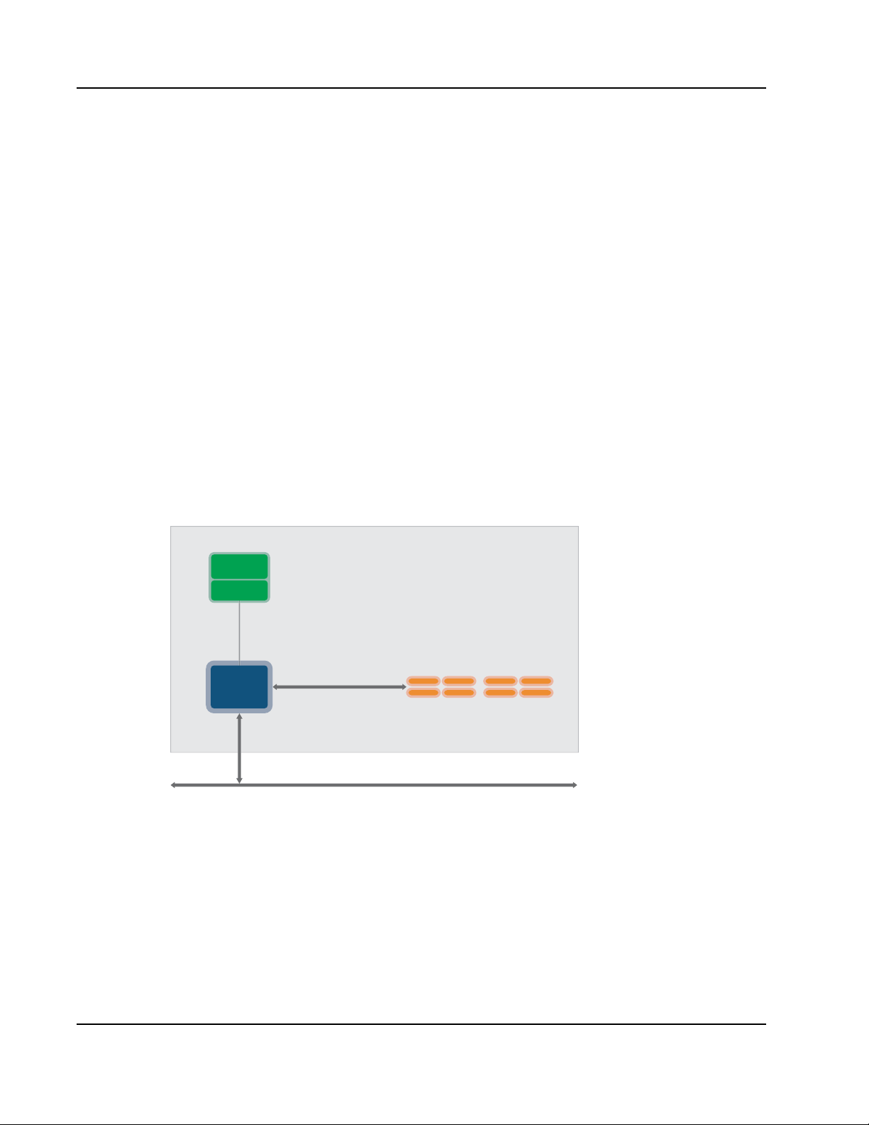
Figure 3: Non-transparent PCI-to-PCI in CompactPCI Application
Because of the non-transparent PCI-to-PCI bridging, the host processor on the CompactPCI a d a p te r
card acts as local host without the local PCI devices being configured by the CompactPC I syst em host.
1.2.2 Primary PCI Interface
The PowerSpan II provides extra functionality for one of the PCI interfaces. The PCI Interface
assigned extra functionality must be specified as Primary PCI Interface through a power-up option.
The Primary PCI Interface functions are:
• CompactPCI Hot Swap Friendly support
• I
O 2.0 Specification compliant messaging
2
• Vital Product Data support.
This extra functionality is available for the Single PCI PowerSpan II and the Dual PCI
PowerSpan II.
Integrated Device Technology
www.idt.com
PowerSpan II User Manual
80A1010_MA001_09
Page 26

1.2.3 PCI Host Bridge
PowerSpan II is designed for host bridge applications. The PowerPC processor generates configuration
cycles on the PCI bus in the same way as that found in conventional PCI host bridges. In addition, with
concurrent reads and low device latency, the PCI Target Interface on PowerSpan II is specifically
designed to allow low latency access to host packet memory for I/O controllers on either of the PCI
buses.
1.2.4 PCI Bus Arbitration
Each PCI Interface has an integrated PCI bus arbiter . Each arbiter su pports four external bus requesters.
An additional three bus requesters can be assigned between the two PCI arbiters.
The PCI arbiters implement a fairness algorithm, two round robin priority levels and flexible bus
parking options.
1.3 Processor Bus Interface
1. Functional Overview26
The PowerSpan II provides a direct-connect 64-bit interface to the PowerQUICC II (MPC8260),
MPC7xx, PowerPC
these interfaces has been extensively verified during product development with processor functional
models as well as with a hardware emulation methodology. This verification ensures any potential
interface issues are identified and resolved by IDT before PowerSpan II customers begin to design their
own systems.
PowerSpan II supports processor (60x) bus extended cycles on the Processor Interface. Extended cycle
support means more flexible bursting and more efficient use of the processor bandwidth.
TM
7xx, and the Wintegra WinPathTM processors. The direct-connect support for
1.3.1 Address Decoding
Instead of consuming chip selects from the processor, PowerSpan II performs its own address decoding
for up to eight memory (slave) images to the PCI bus from the processor bus. This allows a flexible
mapping of processor transactions to PCI cycle types.
1.3.2 Processor Bus Arbitration
The Processor Interface has an integrated bus arbiter. The Processor Interface supports three external
bus masters for applications involving multiple processors. The pro cessor bus arbi ter im plem ents two
levels of priority, where devices programmed into a specific priority level operate in a round robin
fashion in that level.
1.4 DMA Controller
PowerSpan II provides four independent, bidirectional DMA channels. Each DMA channel is capable
of Linked-List or Direct mode transfers.
Each DMA channel transfers data from any-port to any-port. For example, from PCI-1 to PCI-2,
Processor Bus to PCI-1, or Processor Bus and Processor Bus. High throughput data transfer is coup l e d
by flexible endian mapping and a range of status bits mappable to external interrupts.
PowerSpan II User Manual
80A1010_MA001_09
Integrated Device Technology
www.idt.com
Page 27

1. Functional Overview 27
1.5 I2C / EEPROM
1.5.1 EEPROM
PowerSpan II registers can be programmed by data in an EEPROM at system reset. This enables board
designers to set unique identifiers for their cards on the PCI bus at reset, and set various image
parameters and addresses. Configuring PowerSpan II with the EEPROM allows PowerSpan II to
boot-up as a Plug and Play compatible device. PowerSpan II supports reads from, and writes to, the
EEPROM.
1.5.2 I2C
PowerSpan II has a master only I2C bus compatible interface which supports up to eight I2C slave
devices. This interface is used by PowerSpan II for the initialization of registers and for reading and
writing PCI Vital Product Data (VPD).
PowerSpan II also provides a mechanism to perform master read and write operations to EEPROMs or
2
other I
C compatible slave devices.
1.6 Concurrent Reads
PowerSpan II’s Switched PCI architecture enables concurrent reads through a single channel. This
ability greatly reduces read latency, which is often the limiting factor in PCI performance.
1.6.1 PowerSpan II’s Concurrent Read Solution
With PowerSpan II’s concurrent reads, read requests are accepted even while the current read is in
progress. Figure 4 illustrates the concurrent read process with the PowerSpan II.
Integrated Device Technology
www.idt.com
PowerSpan II User Manual
80A1010_MA001_09
Page 28

Figure 4: Concurrent Read Process with PowerSpan II
Master 1: Makes a read request
and is retried.
READ 1 Request
READ 1
Read Request
Master 2: Makes an initial read
request and is retried.
READ 2
Master 1: Takes the read data
Master 2: Takes read data
Read Request
Master 1: Makes request
1. 2.
3. 4.
1. Functional Overview28
When Master 2 makes its first read request in Step 2, it is retried but information about the read request
is latched and initiates a read on the other bus. This occurs even though a read is in progress fo r
Master 1.
PowerSpan II can simultaneously support two reads to the Processor Bus and two reads to the PCI bus.
1.6.1.1 Conventional Reads and Retries
In conventional FIFO-based bridge architectures, bus masters must take turns for read opportunities
and incur multiple retries while waiting. Figure illustrates the read process for subsequent reads where
retries are incurred while a pending read is completed.
PowerSpan II User Manual
80A1010_MA001_09
Integrated Device Technology
www.idt.com
Page 29

1. Functional Overview 29
Master 1: Makes a
read request.
READ 1 Request
1.
Master 1: Takes the read data.
2.
READ 2 Request
Master 2: Makes a read
request and is retried.
Master 2: Makes another
read request.
4.
READ 2
READ 1
Master 1: Makes another
request and is retried.
3.
Master 2: Takes the read data.
6.5.
Figure 5: Reads with Conventional FIFO-Based Bridges
When Master 2 is retried in Step 2, no information is latched about the read request. When Master 2
returns for a subsequent read request in Step 4, it is treated by the bridge as the first read request.
1.6.2 PowerSpan II’s Concurrent Read Applications
1.6.2.1 PCI Host Bridge
In a PCI host bridge application, all of the PCI masters — for example, I/O controllers — potentially
receive only one retry before receiving read data. Even with another read pending, when the PCI T ar get
Interface of the PCI host device receives a read request, it latches the information and begins another
burst read prefetch on the processor bus. The PCI host bridge latches the addresses and delivers the
data to each master using separate, dedicated buffering. This approach greatly reduces the overall
system latency and allows for a more scalable I/O subsystem.
Integrated Device Technology
www.idt.com
PowerSpan II User Manual
80A1010_MA001_09
Page 30

1.6.2.2 Adapter Card
In an adapter card application, the read latency problem is a mirror image of a PCI host bridge
application. In an adapter card, the PowerQUICC II serial ports (FCCs) may be expected to transfer bit
streams through the PowerQUICC II/PCI to host memory across the PCI bus. In this case, ther e can be
eight separate FCCs potentially contending for the processor slave interface in the PCI bridge
assuming there are two PowerQUICC IIs on the local bus. This architecture adds considerable latencies
to read transactions because of FCCs attempting reads to host memory across the PCI bus. Ideally , each
FCC would have a dedicated channel to the PCI bus so they do not have to share resources.
PowerSpan II supports this ideal situation through its concu r rent reads in a flexible switching
architecture. The PCI bridge latches information about the local read as it receives the read request
even with reads pending. The FCCs can now receive transmit data from system host memory with far
lower latencies.
1. Functional Overview30
—
PowerSpan II User Manual
80A1010_MA001_09
Integrated Device Technology
www.idt.com
Page 31

2. PCI Interface
Peripheral Component Interconnect (PCI) is a bus protocol that defines how devices co mmunicate on a
peripheral bus and with a host processor. If a device is referred to as PCI compliant it must be
compliant with the PCI Local Bus Specification (Revision 2.2). A PCI bus supports frequencies up to
66 MHz, and 32-bit or 64-bit transfers.
This chapter describes the PCI Interface of the Dual PCI PowerSpan II. The following topics are
discussed:
• “Overview” on page 31
• “PCI Target Interface” on page 37
• “PCI Master Interface” on page 46
• “CompactPCI Hot Swap Silicon Support” on page 53
• “Vital Product Data” on page 60
• “I2O Shell Interface” on page 62
31
2.1 Overview
This chapter describes the functionality of the Dual PCI PowerSpan II. The Single PCI PowerSpan II is
identified when its functionality or settings differ from the Dual PCI PowerSpan II.
The Single PCI PowerSpan II and the Dual PCI PowerSpan II have different characteristics. The
features of each device are shown in the following list.
• Dual PCI PowerSpan II:
— One 32-bit or 64-bit PCI interface
— One 32-bit interface
— 66 MHz operation
• Single PCI PowerSpan II:
— One 32-bit or 64-bit PCI interface
— 66 MHz operation
2.1.1 Primary PCI
The Dual PCI PowerSpan II has two PCI interfaces: the PCI-1 Interface and the PCI-2 Interface. PCI-1
interface is 32-bit or 64-bit capable, while the PCI-2 Interface is 32-bit. Both PCI interfaces have
66 MHz capability.
Integrated Device Technology
www.idt.com
PowerSpan II User Manual
80A1010_MA001_09
Page 32

2. PCI Interface32
There are two settings available for the Dual PCI PowerSpan II: Primary PCI Interface and Secondary
PCI Interface. The Primary PCI Interface adds extra functionality to the PCI Interface that is designated
as the Primary PCI Interface. The Secondary PCI Interface has no extra functionality.
The following features are associated with the Primary PCI Interface:
• CompactPCI Hot Swap Support (see “CompactPCI Hot Swap Silicon Support” on page 53)
• Vital Product Data (see “Vital Product Data” on page 60)
O Shell Interface (see “I2O Shell Interface” on page 62)
•I
2
The Primary PCI Bus (PRI_PCI) bit in the “Reset Control and Status Registe r” on page 324 is
always 0 in the Single PCI PowerSpan II.
Either the PCI-1 Interface (64-bit) or the PCI-2 Interface (32-bit) can be configured as the Primary
Interface. The selected PCI interface is assigned as the Primary PCI Interface through the Primary PCI
Select (PWRUP_PRI_PCI) power-up option (see “Resets, Clocks and Power-up Options” on page 167
for more information). Primary PCI functionality is shown in the value of the Primary PCI Bus
(PRI_PCI) bit in the “Reset Control and Status Register” on page 324. The PRI_PCI is a status bit and
only shows which bus is primary. It does not enable a bus as the Primary PCI Interface. The Primary
PCI interface is enabled with a power-up option (see 9. “Resets, Clocks and Power-up Options”
on page 167).
2.1.1.1 Clock Frequencies
Each of the PCI interfaces, PCI-1 and PCI-2, run at frequencies from 25 MHz to 66 MHz. The DEV66
bit in the “PCI-1 Control and Status Register.” on page 251 indicates that PowerSpan II is a 66
MHz-capable device.
The speed of these buses is determined through a power-up option (se e “Clocks” on page 170 and
“Power-Up Options” on page 171) using the corresponding P1_M66EN pins.
Both PCI interfaces run asynchronously to one another, and asynchronously to the Processor Bus
Interface.
2.1.2 PCI Data Width
The PCI-1 Interface is a 64-bit data interface that supports 32-bit addressing. The PCI-2 Interface is a
32-bit data interface that supports 32-bit addressing.
2.1.2.1 PowerSpan II in non-Hot Swap and PCI Host Applications
The PCI-1 Interface can be programmed to assert P1_REQ64# to indicate the data width of the PCI-1
bus at reset. This feature is controlled by the PWRUP_P1_R64_EN power-up option (see “Power-Up
Options” on page 171) and minimizes required external logic. A logic low applied to P1_64EN#
enables this feature. PowerSpan II drives P1_REQ64# when PWRUP_P1_R64_EN is selected and
P1_64EN# is set to 0.
PowerSpan II User Manual
80A1010_MA001_09
Integrated Device Technology
www.idt.com
Page 33

2. PCI Interface 33
When P1_64EN# is at a logic low, and PWRUP_P1_R64_EN is selected, P1_REQ64# is asserted low
during reset. The status of PWRUP_P1_R64_EN is reflected in the P1_R64_EN bit in the “Reset
Control and Status Register” on page 324.
This feature must only be used in systems where PowerSpan II controls both P1_REQ64#
and P1_RST#. In this scenario, PowerSpan II is the Central Resource in the system and can
ensure that timing parameters are satisfied.
2.1.2.2 PowerSpan II in non-Hot Swap and PCI Peripheral Applications
The PCI-1 Interface supports the following mechanisms for determining the width of the PCI-1
datapath:
• sampling P1_REQ64# at the negation of P1_RST#
• logic level on P1_64EN#
In non-Hot Swap applications, the P1_64EN# signal must be pulled high in order to enable sampling of
P1_REQ64# to determine the width of the data path. The result of the sampling of P1_REQ64# is or’d
with the logic level on P1_64EN# to determine data path width (see Table 3).
Table 3: Signals Involved in PCI Data Width Determination
Signal
0 0 64-bit bus
1 0 64-bit bus
0 1 64-bit bus
1 1 32-bit bus
2.1.2.3 PowerSpan II in Hot Swap Applications
In Hot Swap applications the P1_64EN# signal is the only signal sampled to indicate the PCI data
width. The following scenarios can be used for determining the proper implementation of the
P1_REQ64# and P1_64EN# signals:
• PCI bus is currently a 32-bit slot and the Hot Swap board is 64-bit capable. In this case,
P1_REQ64# is pulled up in the slot and P1_64EN# is OPEN and the card will initialize in 32-bit
mode.
• PCI bus is currently a 32-bit slot and the Hot Swap board is 32-bit capable. In this case,
P1_REQ64# is not sampled and P1_64EN# does not exist on the board so initi ali zati on would be
32-bit mode.
ResultP1_REQ64# P1_64EN#
Integrated Device Technology
www.idt.com
PowerSpan II User Manual
80A1010_MA001_09
Page 34

• PCI bus is currently a 64-bit slot and the Hot Swap board is 64-bit capable. In this case,
P1_REQ64# could be anything but P1_64EN# is GND and the card will initialize in 64-bit mode.
• PCI bus is currently a 64-bit slot and the Hot Swap board is 32-bit capable. In this case,
P1_REQ64# is not sampled and P1_64EN# does not exist on the board so initialization would be
32-bit mode.
2.1.2.4 PowerSpan II Drives PCI 64-bit Extension Signal in 32-bit Environment
When PowerSpan II's 64-bit PCI interface is programmed to operate in 32-bit mode, the 64-bit
extension PCI bus signals can be left open. PowerSpan II actively drives the following the input
signals:
• Driven Low
— P1_ADb[63:32]#
— P1_CBE[7:4]#
—P1_REQ64#
— P1_ACK64#
—P1_PAR64#
2. PCI Interface34
—P1_PAR64#
— P1_REQ64#
— P1_ACK64#
This insures the signals do not oscillate and that there is not a significant power drain through the input
buffer.
2.1.3 PCI Interface Descriptions
The PowerSpan II PCI interfaces are described in terms of its PCI master and PCI target functions. This
description is largely independent of PCI-1 versus PCI-2, or the assignment of the Primary PCI
Interface functions. Exceptions to these rules are noted as required.
Cross-references to PCI registers are shown as PCI-1 whenever the
cross-references apply equally to PCI-1 or PCI-2 registers.
2.1.4 Transaction Ordering
PowerSpan II implements a set of ordering rules for transactions initiated by master(s) connected to
PCI Interface Px, that are destined for targets and/or slaves connected to PCI Interface Py.
Transactions initiated by master(s) connected to PCI Interface Px, but with different
PowerSpan II destination interfaces, are independent from an ordering perspective.
Transactions initiated by PowerSpan II DMA and PowerSpan II generated interrupt events
have no ordering relationship to externally initiated transactions processed by PowerSpan II.
PowerSpan II User Manual
80A1010_MA001_09
Integrated Device Technology
www.idt.com
Page 35

2. PCI Interface 35
2.1.4.1 Transactions Between Px and Py
PowerSpan II implements the following transaction ordering rules for transactions flowing between
PCI Interface Px and PCI Interface Py:
• The order in which delayed read requests are latched on the source bus, and posted memory write
transactions are presented on the source bus, is the order in which they appear on the destination
bus.
• Writes flowing from Px to Py have no ordering relationship to w rites flo wing from Py to Px.
• The acceptance of a posted write as a target or slave is not contingent on the completion of a
transaction by the master of the same interface. PowerSpan II master and target/slave modules are
independent.
2.1.4.2 Transactions Between the PB Interface and the PCI Interfaces
When there are transactions to the PB Interface from both PCI-1 and PCI-2, there is a possibility that a
transaction from PCI-2 can be queued ahead of a transaction from
PCI-. This is caused by the fact there is no transaction ordering between the two independent PCI
interfaces. For example, if transactions to the PB Interface arrive in the following order from PCI-1 and
PCI-2:
• PCI-1 Write 1
• PCI-2 Write 1
• PCI-2 Write 2
• PCI-1 Write 2
The transactions can be completed to the PB Interface in the following order even though PCI-2 Write
2 entered PowerSpan II before PCI-1 Write 2:
• PCI-1 Write 1
• PCI-2 Write 1
• PCI-1 Write 2
• PCI-2 Write 2
This is caused by the fact that PCI-1 to PB Interface transactions and PCI-2 to PB Interface transactions
arbitrate in a round robin fashion. When a PowerSpan II decision is required on whether to service a
transaction from PCI-1 or PCI-2, writes are available at both even though at one point a write is only
available from PCI-2.
2.1.4.3 DMA Transactions
DMA transactions and regular write/read transactions arbitrate for the use of a master interface in a
round robin scheme. There are no special priorities for DMA transactions and regular write/read
transactions.
Integrated Device Technology
www.idt.com
PowerSpan II User Manual
80A1010_MA001_09
Page 36

Writes and reads from one source are queued and arbitrated for the use of the master interface with
DMA in a round robin design. A DMA transaction can be given a lower priority by programming the
DMA Channel Off Counter (OFF) bit in the “DMA x General Control and Status Register” on
page 314. The OFF bit provides programmable control over the amount of source bus traffic generated
by the DMA channel. The channel interleaves source bus transfers with a period of idle processor bus
clocks where no source bus requests are generate d. When source and destination interfaces are
different, 256 bytes of source bus traffic occurs before the idle period. If source and destination
interfaces are the same, 64 bytes of source bus traffic occur before the idle period. This helps prevent
PowerSpan II from interfering with processor bus instruction fetches.
All transactions (writes/reads/DMA) from two source interfaces arbitrate in a round robin scheme on a
per interface basis. Refer to “Transactions Between the PB Interface and the PCI Interfaces” on
page 35 for more information.
2.1.4.4 PCI Transaction Ordering Rules
The PCI 2.2 Specification outlines transaction ordering rules for PCI transactions. PowerSpan II does
not comply with the following PCI transaction ordering rules:
• PowerSpan II only completes the writes that are destined for the same bus as the initiated read
when it is processing a read request. It does not complete writes in both directions before
processing a read request. PowerSpan II does not prioritize writes over reads.
2. PCI Interface36
• PowerSpan II does not allow posted memory writes to pass delayed read requests. This implies that
deadlock conditions may occur when the customer uses bridges that do not support delayed
transactions. Deadlock conditions are broken by the PowerSpan II maximum retry counter.
PowerSpan II User Manual
80A1010_MA001_09
Integrated Device Technology
www.idt.com
Page 37

2. PCI Interface 37
2.2 PCI Target Interface
PowerSpan II participates in a transaction as a PCI target when a PCI master initiates one of the
following actions:
• attempts to access the alternate PCI Interface
• attempts to access processor bus memory
• accesses PowerSpan II registers
This chapter describes only the first two conditions listed above. Transactions targeted for the
PowerSpan II’s 4 Kbytes of device control and status registers are discussed in “Register Access” on
page 235.
The operation of the PCI Target is described by dividing the PCI transaction into the following phases:
• Address phase: This section discusses the decoding of PCI accesses.
• Data phase: This section describes control of burst length and byte lane management.
• Terminations: This section describes the terminations supported by the PowerSpan II, how they are
mapped from the destination port to the PCI Target, and exception handling.
2.2.1 Address Phase
The address phase deals with the decoding of PCI accesses.
2.2.1.1 Transaction Decoding
Transaction decoding on the PCI Target operates in bo th normal decode mode and Master-based
decode mode. Only memory and conf iguration cycles are decoded. I/O cycles are not decoded.
During normal decode mode, a PCI device monitors the Px_AD and Px_C/BE# lines to decode an
access to some programmed PCI physical address range
A PCI target image is defined as the range of PCI physical address space to decode a PCI transaction. A
PCI target image location and size is controlled using a Base Address field and in the “PCI T ar get Base
Address Register” on page 259, and a Block Size field in the “PCI-1 Target Image x Control Register”
on page 268.
Normal address decoding only applies to memory cycles.
— through positive decoding.
Integrated Device Technology
www.idt.com
PowerSpan II User Manual
80A1010_MA001_09
Page 38

2. PCI Interface38
Table 4 illustrates the command encoding for PowerSpan II as PCI target.
Table 4: Command Encoding for T ransaction Type—PowerSpan II as PCI Target
Px_C/BE#[3:0] Transaction Type PowerSpan II Capable
0000 Interrupt Acknowledge No
0001 Special Cycle No
0010 I/O Read No
0011 I/O Write No
0100 Reserved N/A
0101 Reserved N/A
0110 Memory Read Yes
0111 Memory Write Yes
1000 Reserved N/A
1001 Reserved N/A
1010 Configuration Read Yes (Type 0 only)
1011 Configuration Write Yes (Type 0 only)
1100 Memory Read Multiple Yes
1101 Dual Address Cycle No
1110 Memory Read Line Yes
1111 Memory Write and Invalidate Aliased to Memory Write
The PCI target image decodes and claims PCI transactions and controls how these incoming PCI
transactions are mapped to the destination port on PowerSpan II.
Table 5 describes the programming model for a PCI Target Image Control register.
Table 5: Programming Model for PCI Target Image Control Register
Bits Type Description Default Setting
IMG_EN R/W Enables the PCI target image to decode in the
specified physical address range of memory
space.
Disabled
TA _EN R/W Enables address translation (see “PCI-1 Target
PowerSpan II User Manual
80A1010_MA001_09
Disabled
Image x Translation Address Register” on
page 274).
Integrated Device Technology
www.idt.com
Page 39

2. PCI Interface 39
Table 5: Programming Model for PCI Target Image Control Register
Bits Type Description Default Setting
BAR_EN R/W Enables the PCI Base Address register . When this
bit is set, the Px_BSTx Register is R/W and visible
to Processor Bus access and PCI memory cycles.
When this bit is cleared, the Px_BSTx register
returns only zeros on a read. Writes will have no
effect on Px_BSTx when this bit is cleared.
BS[3:0] R/W Sets the block size of the PCI target image. The
size of the image is 64Kbyte * 2
MODE R/W Maps the incoming PCI transaction to either
memory or I/O space on the alternate PCI bus.
DEST R/W Directs the incoming PCI transaction to eit her the
processor bus or the alternate PCI interface.
MEM_IO R/W Commands to the corresponding image generates
Memory Read commands on the destination PCI
bus (Py) with the same byte enables latched from
the source bus transaction PowerSpan II is
capable of performing 1,2,3, or 4 byte memory
transfers on the PCI bus(es).
RTT[4:0] R/W A 5-bit value, defined in the processor bus
protocol, is generated on the PB_TT lines during a
read on the processor bus.
BS
.
Enabled or configurable
through EEPROM
Default value is 0, can be
programmed through any
port after reset or loaded
through EEPROM.
Default value is 0 (Memory
command generation)
Defaults to processor bus
Default value is 0 (Regular
I/O mode)
Defaults to Read
GBL R/W Controls the assertion of the PB_GBL_ cache
control signal.
CI_ R/W Controls the assertion of the PB_CI_ cache
control signal.
WTT[4:0] R/W A 5-bit value, defined in the processor bus
protocol, is generated on the PB_TT lines during a
write on the processor bus.
PRKEEP R/W Enables PowerSpan II to keep prefetch read data
over subsequent transactions (see “Reads” on
page 41).
END[1:0] R/W Sets endian mapping to little-endian, PowerPC
little-endian, or big-endian (see “Endian Mapping”
on page 177).
Asserts PB_GBL_
Asserts PB_CI_
Defaults to Write with Flush
Disabled
Big-endian is the default
mode.
Integrated Device Technology
www.idt.com
PowerSpan II User Manual
80A1010_MA001_09
Page 40

Table 5: Programming Model for PCI Target Image Control Register
Bits Type Description Default Setting
2. PCI Interface40
MRA R/W Aliases a Memory Read Command to Memory
Read Multiple Command. This causes Po werS pan
II to prefetch read data on the destination bus
(processor bus or PCI) up to the amount
programmed in the RD_AMT[2:0] field.
RD_AMT[2:0] R/W Controls the prefetch read amount for a Memory
Read when MRA is enabled. Memory Read
Multiple always causes prefetch up to the value in
RD_AMT[2:0]. This can be programmed up to a
maximum of 128 bytes.
Disabled
8 bytes is the default
prefetch read amount
Master-based Decode
The PCI T a rget supports Master-based decode when the PowerSpan II PCI arbiter is enabled (see
“Arbitration” on page 137). With Master-based decode enabled, a PCI target image only claims a
transaction decoded for its specified physical address space if it originates from a specific PCI master.
External bus masters are selected for a specific target image by setting the corresponding bits in the
“PCI-1 Target Image x Tra nslation Address Register” on page 274.
PowerSpan II behavior is undefined if more than one overlapping target image claims a
transaction. For example, if two target image have the same base address and size, then they
must have unique master bits set in the “PCI-1 Target Image x Translation Address Register”
on page 274.
2.2.1.2 Address Translation
The address generated on the destination port is dependent on the use of address translation in the
source target image. For more information, see the Translation Address Enable (TA_EN) bit in the
“PCI-1 Target Image x Control Register” on page 268. When address translation is enabled
setting the TA_EN bit
— the address generated on the destination bus is derived from the following
three inputs:
• incoming address on the PCI Target
• block size of the target image
BS[3:0] in the “PCI-1 Target Image x Control Register” on page 268
• translation address
TADDR in the “PCI-1 Target Image x Translation Address Register” on page 274
When address translation is disabled the address on the destination bus is the same as the address on the
source bus.
2.2.1.3 Transaction Type Mapping
A transaction can be mapped to the PB interface or to another PCI Interface.
— by
PowerSpan II User Manual
80A1010_MA001_09
Integrated Device Technology
www.idt.com
Page 41

2. PCI Interface 41
Mapping to the Processor Interface
The PCI T arget Image controls the transaction type on the processor bus through the use of the PB
Read Transfer Type (RTT[4:0]) and PB Write Transfer Type (WTT[4:0]) bits in the “PCI-1 Target
Image x Control Register” on page 268. By default, these bit fields assign reads as read operations on
the processor bus, and assign incoming writes as Write with Flush on the Processor Bus.
Mapping to a PCI Interface
The PCI T arget Image determines the address space on the destination PCI bus through the use of the
Image Mode (MODE) bit in the “PCI-1 Target Image x Control Register” on page 268. By default,
incoming PCI transactions are mapped to Memory Space on the alternate PCI Interface. Setting the
MODE bit maps incoming PCI transactions to
I/O Space on the alternate PCI Interface.
2.2.1.4 Address Parity
The PCI target image monitors parity during the address phase of decoded transactions. Address parity
errors are reported on Px_SERR# when both the Parity Error Response (PERESP) and SERR Enable
(SERR_EN) bits are set in the “PCI-1 Control and Status Register.” on page 251. Assertion of the
Px_SERR# signal can be disabled by clearing the SERR_EN bit.
PowerSpan II records an error condition in the event of an address parity error (see “Error Handling”
on page 157). PowerSpan II claims the errored transaction and forwards the transaction to the
destination bus.
2.2.2 Data Phase
The data phase deals with control of burst length and byte lane management.
2.2.2.1 Writes
PowerSpan II accepts single beat or burst transactions in memory space. I/O accesses are not decoded.
All writes to the PCI Target are posted writes.
Burst writes are linear bursts. A Target-Disconnect is issued if a buffer fills while a burst write is in
progress (see “Termination Phase” on page 44). PowerSpan II can manage arbitrary PCI byte enable
combinations during PCI burst writes.
PowerSpan II does not support delayed write transactions as described in the PCI 2.2
Specification.
2.2.2.2 Reads
PowerSpan II supports up to four concurrent reads from external PCI masters. All four reads are treated
equally and have the same prefetch capacity, but have individually programmable values .
Integrated Device Technology
www.idt.com
PowerSpan II User Manual
80A1010_MA001_09
Page 42

2. PCI Interface42
Processor Bus
PCI Bus
RET-A RET-B RET-A RET-B ACC-A Completion-A ACC-B Completion-B
PPC-RDB
PPC-RDA
Device,
Arbitration and
Memory Latency
Arbitration and
Memory Latency
Single Read Latency
Double Read Latency
An example of PowerSpan II’s concurrent read capability is illustrated in Figure 6. The concurrent
reads in the figure are represented by Read A and Read B. In the figure, both Read A and Read B are
retried. Once Read A is completed on the processor bus, Read B is initiated on the processor bus while
the contents of Read A are returned to the PCI master. Because Read B is completed on the processor
bus while Read A data is returned to the PCI bus, read latency is significa nt ly reduced with concurrent
reads.
Figure 6: Concurrent Read Waveform
See “Concurrent Reads” on page 27 for a general discussion of read pipelining in PowerSpan II.
Concurrent Read Phases
The delayed, concurrent reads on the PCI Target consist of the following phases:
1. Delayed Read Request
– The PCI Target latches the transaction parameters and issues a retry.
2. Delayed Read
– The PCI Target obtains the requested data. The destination bus master retries requested
data.
3. Delayed Read Completion
– The master repeats the transaction with the same parameters used for the initial request
and data is provided by PowerSpan II.
Read line buffers are allocated on a first come, first serve basis. When an external master makes the
initial memory request, the PowerSpan II PCI Target captures the PCI address in an available delayed
read request latch. This initiates a read on the destination bus specified by the Destination Bus (DEST)
bit in the “PCI-1 Target Image x Control Register” on page 268.
Prefetch Reads
All PowerSpan II PCI target memory reads are considered prefetchable to 8-byte boundaries by
default. Setting the MEM_IO bit in the “PCI-1 Target Image x Translation Address Register” on
page 274 enables 1,2,3, or 4 byte memory reads on the PCI bus and 4 byte reads on the processor bus.
When PowerSpan II is programmed to support 4 byte transactions, only 4 byte transactions are
supported. Burst transactions are not supported while the MEM_IO bit is set to 1.
PowerSpan II User Manual
80A1010_MA001_09
Integrated Device Technology
www.idt.com
Page 43

2. PCI Interface 43
In order to program PowerSpan II to complete 4 byte reads on the PCI bus, both the MEM_IO bit and
the MODE bit must be set to 1 in the PCI x Target Image x Control register.
In order to perform a 4-byte read from the PCI bus to the processor (60x) bus, the following bits must
be programmed:
• MEM_IO bit set to 1
• MODE bit set to 1 or 0
• END bit, in the “PCI-1 Target Image x Control Register” on page 268, must not be set to
little-endian mode (00). It can be set to PowerPC little-endian (01), or big-endian (10).
When the Target Image Control register is programmed for 4 byte read transactions,
requesting 8 byte reads causes undefined results in the system.
PowerSpan II prefetch behavior on the destination bus when claiming Memory reads on the originating
bus is controlled by the PCI Memory Read Alias (MRA) bit and the Prefetch Size (RD_AMT[2:0])
field in the “PCI-1 Target Image x Control Register” on page 268. If the MRA bit is set when
PowerSpan II claims a memory read, PowerSpan II prefetches the amount programmed into the
RD_AMT[2:0] field
— up to 128 bytes.
The Memory Read Line command results in a prefetch of the value programmed into Cache Line
(CLINE) bit. When the MRA bit is cleared, the target image prefetches 8 bytes when a PCI Memory
Read command is decoded.
The Memory Read Multiple command results in a prefetch read of a mini mum of 32 bytes or the val ue
programmed into the RD_AMT[2:0] field
— independent of the MRA bit setting.
The PowerSpan II PCI target read watermarks are defined in Table 6.
Table 6: PowerSpan II PCI Ta rg e t Re ad Watermarks
PCI Command Prefetch Amount
Memory Read 8 bytes (default) or 1,2,3, or 4 bytes
Depending in the setting in the MEM_IO bit in
the “PCI-1 Target Image x Control Register” on
page 268
Memory Read Line Minimum of CLINE in the “PCI-1
Miscellaneous 0 Register” on page255
register
Memory Read Multiple Minimum of 32 bytes or RD_AMT.
PowerSpan II never prefetches data beyond a 4-Kbyte address boundary regardless of the value
programmed in the RD_AMT field. This boundary corresponds to the processor bus memory
management page size.
Integrated Device Technology
www.idt.com
PowerSpan II User Manual
80A1010_MA001_09
Page 44

The PowerSpan II PCI Target can be configured to keep prefetch data over multiple read accesses for
any master that provides the correct ad dress
x Control Register” on page 268. PowerSpan II increments its latched address for the read transaction
based on the amount of data removed by the PCI master during the read transaction. If the PCI master
returns with an address that matches the incremented address held by PowerSpan II, then PowerSpan II
provides data already held in the prefetch line buffer.
Writes do not invalidate read buffer contents.
2.2.2.3 Data Parity
PowerSpan II monitors Px_PAR#/Px_PAR64# when it accepts data as a PCI target during a write.
PowerSpan II drives Px_P AR#/Px_PAR64# when it provides data as a PCI target during a read. In both
cases, the Px_PAR#/Px_PAR64# signal provides even parity for Px_C/BE#[3:0] and Px_AD[31:0] —
or Px_C/BE#[7:4] and Px_AD[63:32] for the PCI-1 Interface in 64-bit mode.
The PERESP bit in the “PCI-1 Control and Status Register.” on page 251 determines whether or not
PowerSpan II responds to parity errors as a PCI target. Data parity errors are reported through the
assertion of Px_PERR# when the PERESP bit is set. The Detected Parity Error (D_PE) bit in the
“PCI-1 Control and Status Register.” on page 251 is set when PowerSpan II encounters a parity error as
a PCI target on any transaction. PowerSpan II records an error condition when a parity error occurs (see
“Error Handling” on page 157).
2. PCI Interface44
— by setting the PRKEEP bit in the “PCI-1 Target Image
2.2.3 Termination Phase
This section describes the terminations supported by the PowerSpan II, how they are mapped from the
destination port to the PCI Target, and exception handling.
2.2.3.1 PCI Target T erminations
The PCI T arget Interface generates the following terminations:
1. Target-Disconnect (with data): A termination is requested by the PCI target — by asserting
Px_STOP# and Px_TRDY# — when it requires a new address phase. Ta rget-Disconnect means the
transaction is terminated after one or more valid data transfers.
The PCI target requests a Target-Disconnect in the following cases:
• PowerSpan II is unable to buffer an incoming write or provide data from a read buffer during a
read.
• PowerSpan II reaches the 4-Kbyte address boundary on reads and writes to the processor bus.
• One data phase for PowerSpan II register accesses
• One data phase for I
• Detection of a transaction with non-linear addressing
O shell accesses
2
PowerSpan II User Manual
80A1010_MA001_09
Integrated Device Technology
www.idt.com
Page 45

2. PCI Interface 45
2. Target-Retry: A termination is requested — by asserting Px_STOP# and Px_DEVSEL# while
Px_TRDY# is high — by the PCI T arget because it cannot currently process the transaction. Retry
means the transaction is terminated after the address phase without any data transfer. PowerSpan II
retries read requests while it fetches data from the desti nation bus. Any att empt by a PCI master to
complete the memory read transaction is retried by the PCI target until at least an 8-byte quantity is
15
available in the line buffer. If a PCI master does not retry the transaction within 2
clocks after a
read request has been latched, the delayed read request latch and line buffer are de-allocated. This
prevents deadlock conditions.
3. T ar get-Abort: The PCI target requests a termination of a transaction — by negating Px_DEVSEL#
and Px_TRDY# and asserting Px_STOP# on the same clock edge — when it cannot respond to the
transaction, or during a fatal error. A fatal error occurs when: a bus error is experienced on the
processor bus, the maximum retry count is exceeded, a Target-Abort occurs on the alternate PCI
bus during a read, or a Master-Abort occurs on the alternate PCI bus during a read.
Although there may be a fatal error for the initiating application, the transaction completes
gracefully, ensuring normal PCI operation for other PCI resources. PowerSpan II sets the signaled
Target-Abort (S_TA) bit in the “PCI-1 Control and Status Register.” on page 251, and records an
error condition in the event of a Target-Abort (see “Error Handling” on page 157)
Error Logging and Interrupts
The PowerSpan II PCI T arget records errors under the following conditions:
• address parity error
• data parity error on writes
• Target-Abort
See “Error Handling” on page 157 and “Interrupt Handling” on page 145 for a full description of error
logging support and associated interrupt mapping options.
Integrated Device Technology
www.idt.com
PowerSpan II User Manual
80A1010_MA001_09
Page 46

2.3 PCI Master Interface
In order for PowerSpan II to be a PCI master in a transaction the Bus Master (BM) bit, in the “PCI-1
Control and Status Register .” on page 251, must be set. With this bit set, PowerSpan II is PCI Master in
a transaction in the following instances:
• Servicing a request by:
— the processor bus: PowerSpan II is accessed as a PB slave
— the alternate PCI Interface: PowerSpan II is accessed as a PCI target
• processing a transfer by one of the four PowerSpan II DMA channels
• generating a configuration or IACK cycle because of a PowerSpan II register access
This section discusses only the first three conditions listed above. Configuration and IACK cycles are
discussed in “Configuration and IACK Cycle Generation” on page 246.
The operation of the PCI Master is described by dividing the PCI master transaction into the following
phases:
• Arbitration phase: This section describes how PowerSpan II requests the PCI bus and its response
to bus parking.
2. PCI Interface46
• Address phase: This section discusses the generation of the PCI address and command encoding.
• Data phase: This section describes control of burst length.
• Terminations: This section explains the terminations supported by
PowerSpan II, how they are mapped to the source port (Processor Interface or the alternate PCI
Interface), and exception handling.
PowerSpan II cannot be both master and target on a PCI bus at the same time.
PowerSpan II User Manual
80A1010_MA001_09
Integrated Device Technology
www.idt.com
Page 47

2. PCI Interface 47
2.3.1 Arbitration Phase: Arbitration for the PCI Bus
PowerSpan II issues a bus request on the PCI bus when it requires access to the PCI bus. When the
PowerSpan II PCI arbiter is active, this request is internal. When it is not enabled the request appears
externally (see “PCI Interface Arbitration” on page 137 for more information).
The internal PowerSpan II PCI arbiter parks the bus on a PCI master by asserting Px_GNT# to the PCI
master. Bus parking improves the performance of the PowerSpan II PCI Master by reducing arbitrati on
latency.
2.3.2 Address Phase
The address phase deals with the generation of the PCI address and command encoding.
2.3.2.1 Command Encoding
The encoding on the Px_C/BE# lines indicate the transaction type on the PCI bus. The PCI command
encoding supported by PowerSpan II, and their corresponding transaction types, are shown in Table 7.
Integrated Device Technology
www.idt.com
PowerSpan II User Manual
80A1010_MA001_09
Page 48

2. PCI Interface48
Table 7: Command Encoding for Transaction Type (PowerSpan II as PCI Maste r )
Px_C/BE# [3:0] Transaction Type PowerSpan II Capable
0000 Interrupt Acknowledge Yes (see “Configurat ion and IACK
Cycle Generation” on page 246)
0001 Special Cycle No
0010 I/O Read Yes
0011 I/O Write Yes
0100 Reserved N/A
0101 Reserved N/A
0110 Memory Read Yes
0111 Memory Write Yes
1000 Reserved N/A
1001 Reserved N/A
1010 Configuration Read Yes (see “Config uration and IACK
Cycle Generation” on page 246)
1011 Configuration Write Yes (see “Configuration and IACK
Cycle Generation” on page 246)
1100 Memory Read Multiple Yes
1101 Dual Address Cycle No
1110 Memory Read Line Yes
1111 Memory Write and Invalidate
(The MWI_EN bit is
hard-wired to “0” in the
“PCI-1 Control and Status
Register.” on page 251)
No
A new request for access to the bus is generated by the PowerSpan II PCI Master when it requires
access to the PCI bus to service a request from the Processor Bus Interface or the other PCI interface
(Py). After the request is generated by PowerSpan II, it successfully arbitrates for access to the PCI bus
when it receives GNT_ from the arbiter. PowerSpan II then asserts Px_FRAME# to indicate the
beginning of a transaction.
PowerSpan II User Manual
80A1010_MA001_09
Integrated Device Technology
www.idt.com
Page 49

2. PCI Interface 49
2.3.2.2 Address Translation
The address generated by the PCI Master is dependent on the use of address translation in the source
target image (see “PCI-1 Target Image x Control Register” on page 268) or slave image (see
“Processor Bus Slave Image x Control Register” on page 287). When address translation is enabled
—
by setting the TA_EN bit in PCI Target or PB Slave Image Control Register — PowerSpan II produces
the PCI address using the following inputs:
• the incoming address from the source bus
• the block size of the slave or target image
• the translation offset
For address translation going from the processor bus to PCI, see “Processor Bus Interface” on page 83.
For an example of address translation control going from PCI to PCI, see “PCI-1 Target Image x
Translation Address Register” on page 274.
When address translation is disabled, the address generated by the PCI Master is the same as the
address on the source bus.
Integrated Device Technology
www.idt.com
PowerSpan II User Manual
80A1010_MA001_09
Page 50

2.3.3 Data Phase
The data phase deals with the control of burst length.
2.3.3.1 Writes
For non-DMA writes, the length of the PCI write transaction is dependent on the length of the
transaction delivered from the source bus. Writes originating from the processor bus can be either
single cycle writes or burst writes. Burst writes from the processor bus are always 32 bytes in length.
This burst is converted to an 8 byte burst on a 32-bit PCI bus. Either PCI-1 or PCI-2 can be configured
as 32-bit. Single cycle writes from the 64-bit processor bus are translated in to two 8 byte burst writes
on the 32-bit PCI bus. This information is summarized in Table 8
Table 8: PB Writes and Their Corresponding PCI Writes
PB Write 64-bit PCI Write 32-bit PCI Write
32-byte Line Write 4-beat 32-byte Burst Write 8-beat 32-byte Burst Write
8-byte Single Write Single Beat 8-byte Write 2-beat 8-byte Burst Write
2. PCI Interface50
The PB Master can also generate extended cycles. Extended cycles are either 16 byte or 24 byte
transactions. These cycles are enabled by setting the Extended Cycle (EXTCYC) bit to 1 in the
“Processor Bus Miscellaneous Control and Status Register” on page 304.
When the Dual PCI PowerSpan II is used, incoming PCI writes are executed as similar writes on the
alternate PCI interface. For example, a 64-byte burst write to memory space from the PCI-1bus is
executed as a 64-byte burst write to the memory space on the PCI-2 bus, provided the target on PCI-2
does not disconnect.
DMA Writes
The PowerSpan II DMA channels always attempt to perform the longest possible burst — up to
128-bytes
2.3.3.2 Reads
The minimum memory read prefetch quantity is 8 bytes (default). Setting the MEM_IO bit in the
“PCI-1 Target Image x Control Register” on page 268 enables 1,2,3, or 4 byte memory reads on the
PCI bus.
Write transactions intended for I/O space on the alternate PCI bus must be single
beat writes. Bursting is not supported for a target image programmed to ge nerate
an I/O access on the alternate PCI bus. A burst write directed at such a target
image results in a Target-Disconnect after every data beat.
— on the PCI bus.
PowerSpan II User Manual
80A1010_MA001_09
Integrated Device Technology
www.idt.com
Page 51

2. PCI Interface 51
The PowerSpan II PCI Master generates a Memory Read command selection according to the rules in
Table 9.
Table 9: PowerSpan II PCI Master Read Commands
Internal Request of Transaction
Length
<= 8 bytes Memory Read
<= CLINE[7:0] in Px_MISC0 Memory Read Line
> CLINE[7:0] in Px_MISC0 Memory Read Multiple
PCI Memory Read Command
The read amount presented to the PCI Master determines the command used. A Memory Read Line
command uses the burst length programmed into the CLINE[7:0] field in the “PCI-1 Miscellaneous 0
Register” on page 255. It is programmable to 16-, 32-, 64-, or 128 bytes.
If the PCI Master does not complete the burst read transaction before a target termination, it
completes the read with subsequent PCI read transactions at the appropriate address.
2.3.3.3 Parity Monitoring and Generation
PowerSpan II monitors Px_PAR#/Px_PAR64# when it accepts data as a PCI master during a read, and
drives Px_PAR#/Px_PAR64# when it provides data as a PCI master during a write. PowerSpan II also
drives Px_PAR#/Px_PAR64# during the address phase of a transaction when it is a PCI master . In both
address and data phases, the Px_PAR#/Px_PAR64# signal provides even parity for Px_C/BE#[3:0] and
Px_AD[31:0]. Even parity is enabled Px_C/BE#[7:4] and Px_AD[63:32] for PCI-1 in 64-bit mode.
PowerSpan II parity response is enabled through the Parity Error Response (PERESP) bit in the “PCI-1
Control and Status Register.” on page 251. Data parity errors are reported through the assertion of
Px_PERR# when the PERESP bit is set. The Detected Parity Error (D_PE) bit in the “PCI-1 Control
and Status Register.” on page 251 is set when PowerSpan II encounters a parity error as a PCI master
on any transaction. PowerSpan II records an error condition in the event of a parity error (see “Error
Handling” on page 157).
The Master Data Parity Detected (MDP_D) bit in the “PCI-1 Control and Status Register.” on page 251
is set if the PERESP bit is enabled and either PowerSpan II is the master of the transaction where it
asserts PERR#, or the addressed target asserts PERR#. If the transfer originated from the Processor
Interface, then PowerSpan II sets the MDP_D bit and the Px_PB_ERR_EN bit in the “Interrupt Enable
Register 1” on page 334. PowerSpan II then asserts an interrupt (see “Interrupt Handling” on
page 145).
PowerSpan II continues with the transaction independent of any parity errors reported during
the transaction.
Integrated Device Technology
www.idt.com
PowerSpan II User Manual
80A1010_MA001_09
Page 52

2.3.4 Terminations
This section describes the terminations supported by the PowerSpan II, how they are mapped from the
destination port to the PCI Target, and exception handling.
2.3.4.1 PCI Master Te rminations
The PCI Master supports all four types of PCI terminations:
1. Master-Abort: The PCI Master negates Px_FRAME# and then negates Px_IRDY# on the
following clock edge when no target responds with Px_DEVSEL# asserted on the fifth positive
edge of clock after Px_FRAME# is asserted. PowerSpan II sets R_MA in Px_CSR and records an
error condition in the event of a Master-Abort (see “Error Handling” on page 157)
2. PCI Interface52
2. Target-Disconnect (with data): A termination is requested by the target
Px_DEVSEL# and Px_TRDY# — because it is unable to respond within the latency requirements
of the PCI 2.2 Specification or it requires a new address phase. Target-Disconnect means the
transaction is terminated after data is transferred. PowerSpan II negates Px_REQ# for at least two
clock cycles if it receives Px_STOP# from the PCI target.
3. Target-Retry: Termination is requested
Px_TRDY# is high — by the target because it cannot currently process the transaction. Retry
means the transaction is terminated after the address phase without data transfer. PowerSpan II has
a Maximum Retry Counter (MAX_RETRY) in the “PCI-1 Miscellaneous Control and Status
Register” on page 283 which is used to record an error condition if the number of retries exceed the
programmed amount (see “Error Handling” on page 157).
4. T arget-Abort: The target requests a termination of a transaction
asserting Px_STOP# on the same clock edge
during a fatal error. Although there may be a fatal error for the initiating application, the
transaction completes gracefully, ensuring normal PCI operation for other PCI resources.
PowerSpan II sets R_TA in Px_CSR and records an error condition in the event of a Ta rget-abort
(see “Error Handling” on page 157).
2.3.4.2 Error Logging and Interrupts
The PowerSpan II PCI Master records errors under the following conditions:
• Data Parity on reads
(when the PERSP bit, in the “PCI-1 Control and Status Register.” on
page 251, is set)
— by asserting Px_STOP,
— by asserting Px_STOP# and Px_DEVSEL# while
— by negating Px_DEVSEL# and
— when it cannot respond to the transaction, or
•Master-Abort
• Target-Abort
• Expiration of Maximum Retry Counter (when the MAX_RETRY field, in the “PCI-1
Miscellaneous Control and Status Register” on page 283, is set.
See “Error Handling” on page 157 and “Interrupt Handling” on page 145 for a full description of error
logging support and associated interrupt mapping options.
PowerSpan II User Manual
80A1010_MA001_09
Integrated Device Technology
www.idt.com
Page 53

2. PCI Interface 53
2.4 CompactPCI Hot Swap Silicon Support
CompactPCI’s Hot Swap Specification defines the process for installing and removing adapter boards
without adversely affecting a running system. It provides a programmatic acce ss to Hot Swap services.
This enables system re-configuration and fault recovery to take place with no system down time and
minimum operator interaction.
PowerSpan II is compliant with the CompactPCI’s Hot Swap Specification, Revision 2.0 and is a Hot
Swap Silicon device. Hot Swap Silicon support includes the following:
• Open drain output pin ENUM# is used to indicate Hot Swap insertion and extraction events.
• 5V tolerant input pin ES for sensing the state of the ejector switch used to insert or extract a
CompactPCI board.
• 5V tolerant open drain output pin LED# for controlling the blue Light Emitting (LED) required to
indicate status of the software connection process.
For the different levels of Hot Swap support, refer to the CompactPCI Hot Swap Specification.
To simplify the design of CompactPCI Hot Swap adapter cards, PowerSpan II has additional support.
This support includes:
• A 5V tolerant input pin HEALTHY# for sensing the status of the Back End power on the card.
• An input pin P1_64EN# that enables Hot Swap adapter cards to sense the presence of a 64-bit PCI
backplane.
2.4.1 LED Support
The LED can be controlled by hardware and software. PowerSpan II drives the LED# signal low to
turn on the LED during the Physical and Hardware Connection process (when HEALTHY# is
negated). A blue LED with an internal resistor can be directly connected between the 5V rail and the
LED# signal. Software controls the LED by setting the LED On/Off (LOO) bit in the “PCI-1 Compact
PCI Hot Swap Control and Status Register” on page 264.
2.4.2 ES Input
The CompactPCI Hot Swap Specification defines a switch located in the ejector handle that indicates to
PowerSpan II if the ejector handle is open or closed. A low value on ES input indicates that the ejector
latch is open. A high value on ES indicates that the ejector latch is closed and is in operation mode.
2.4.3 HEALTHY# Signal
PowerSpan II manages the electrical board level issues involved in the Hot Swap process with the
HEALTHY# signal. The negation of HEALTHY# indicates only some of the components on the Hot
Swap card are powered. T o operate in this environm ent and minimize long term reliability issues, the
HEALTHY# signal controls the electrical behavior of PowerSpan II I/O buffers.
Integrated Device Technology
www.idt.com
PowerSpan II User Manual
80A1010_MA001_09
Page 54

During the negation of HEALTHY#, PowerSpan II disables its output and bidirectional pins (except for
LED#) to avoid applying power to non-powered components on the card. The signals connected
between PowerSpan II and these non-powered components result in floating pins on PowerSpan II.
PowerSpan II uses HEALTHY# to inhibit the input receivers. An inhibited receiver has no static
current path between supply and ground that could be activated by a voltage level near the switching
point.
See “Resets, Clocks and Power-up Options” on page 167 for more details on HEALTHY# and
PowerSpan II reset.
2.4.4 CompactPCI Hot Swap Card Insertion and Extraction
A CompactPCI board has a staggered pin arrangement (long/medium/short) to allow power and
ground, signal and a Board Inserted Indicator (BD_SEL#) to be connected and disconnected in stages.
A limited number of power and ground pins are long. The rest of the power, ground, and signal pins are
of medium length. BD_SEL# is a short pin. When BD_SEL# connects, the physical connection process
is complete.
2.4.4.1 CompactPCI Hot Swap Process
A CompactPCI Hot Swap board is divided into two power regions: Early Power and Back End Power.
Early Power is provided by th e lo ng p ins on the Comp actPCI conn ecto r. Back End Power is controlled
by a sequencer on the card. The sequencer begins to power the Back End of the card when the short
CompactPCI signal BD_SEL# engages on insertion, or when host software enables the process as in a
High Availability system.
2. PCI Interface54
In Figure 7, PowerSpan II is designed into a CompactPCI adapter card.
Figure 7 assumes the CompactPCI backplane is not in reset during the insertion and
extraction process. For example, PowerSpan II’s P1_RST# is negated.
PowerSpan II User Manual
80A1010_MA001_09
Integrated Device Technology
www.idt.com
Page 55

2. PCI Interface 55
Long Pins
Short Pins
Long Pins
Medium
Pins
5 V
VIO
Rp
GND
Rp
Vp
Precharge
Regulator
5 V
3.3v
2.5v
P1_RST_DIR
"remaining PCI-1 I/O"
PB_RST_DIR
PB_CLK
"remaining PB I/O"
P2_RST_DIR
P2_CLK
"remaining PCI-2 I/O"
GND
LED#
ES
Long Pins
Ejector/Switch
Early Power
5 V
3.3 V
HEALTHY#
GND
Hot Swap
Supply Sequencer
5 V
3.3 V
Power On
Reset
Oscillator
Regulator
Back End Power
3.3 V
2.0 V
CLKIN
"remaining I/O"
GND
Host Processor
RST#
CLK
"remaining I/O"
GND
Secondary PCI
3.3 V
BD_SEL#
HEALTHY#
P1_RST#
ENUM#
P1_64EN#
P2_RST#
PB_RST_
3.3 V
PO_RST_
Compact PCI PCI-1/J1 Connector
GND
PORESET_
HRESET_
ON_
PowerSpan II
Figure 7: PowerSpan II in a CompactPCI Adapter Card
Integrated Device Technology
Ensure that PB_CLK and P2_CLK are within specification before the release of back-end
power-up reset.
www.idt.com
PowerSpan II User Manual
80A1010_MA001_09
Page 56

2.4.5 Hot Swap Insertion Process
Use the application illustrated in Figure 7 as a point of reference in the Hot Swap insertion process
outlined below.
1. Long pins contact for Early Power:
— HEALTHY# negated
– PowerSpan II resources are in reset
– LED# pin enabled, st atus diode turned on
– PowerSpan II output pins disabled, input pins inhibited
— Card’s PCI signals pre-charge
2. Medium pins contact PCI backplane signals:
— PowerSpan II’s Primary PCI Interface, in this case PCI-1, connects to the PCI pins on the
backplane
— PowerSpan II P1_CLK is within specification
3. Short pins contact, BD_SEL# asserted:
2. PCI Interface56
— Back End Power ramps
— Back End Power-up reset asserted
– PowerSpan II PO_RST_ asserted
– Host processor PORESET_ asserted, Host processor asserts HRESET_
— Clock generator begins oscillation
– PowerSpan II PB_CLK and P2_CLK begin to oscillate
— Ejector switch closes sometime after short pins contact
4. Back End power is within specification:
— HEALTHY# asserted
– LED# pin disabled
– PowerSpan II outputs enabled, PB_RST_ and P2_RST# asserted
— Host processor and Secondary PCI clocks are within specification
5. Back End Power-up reset negation:
— PowerSpan II PLLs released from reset and begin to lock on to P1_CLK, PB_CLK, P2_CLK
PowerSpan II User Manual
80A1010_MA001_09
Integrated Device Technology
www.idt.com
Page 57

2. PCI Interface 57
— Host processor completes its configuration master transactions
– PowerSpan II power-up options are loaded
— Host processor HRESET_ times out
— PowerSpan II PLL locking complete
– All PowerSpan II resources out of reset, PB_RST_ and P2_RST# negated
– PowerSpan II executes EEPROM load or waits to be initialized by the processor
6. PowerSpan II waits for the closed ejector switch and responds by:
— Setting INS bit in the HS_CSR register
— Asserting ENUM#
7. PowerSpan II is now able to accept Configuration cycles on PCI-1 from the CompactPCI Host
Since Px_LOCKOUT bit in the “PCI-1 Miscellaneous Control and Status Register” on page 283)
defaults to 1, PowerSpan II retries the Host Configuration accesses on the PCI-1 Interface until
Px_LOCKOUT is cleared. The Host then negates ENUM# by clearing the Insertion (INS) bit in the
“PCI-1 Compact PCI Hot Swap Control and Status Register” on page 264 and configures the card. The
Px_LOCKOUT bit is cleared by an EEPROM load or by access from the Processor Interface. It is
automatically cleared by PowerSpan II when the PWRUP_BOOT option is set to PCI.
Integrated Device Technology
www.idt.com
PowerSpan II User Manual
80A1010_MA001_09
Page 58

Figure 8: Hot Swap Insertion
EXT bit
INS bit
LED
ENUM#
Ejector State
PCI Signals
PCI Clock
PCI RST#
HEALTHY#
BD_SEL#
Back End Power
Early Power
Med
Engage
Short
Engage
Fully
Seated
Clocking
Closed
Open
Engaged, tracking bus
Cleared/Unarmed
Cleared/Armed
LED off
Cleared/Unarmed
Set
Cleared/Unarmed
Physical Connection
Hardware Connection
Start of Software Connection Process
LED on
pre-charge
Pulled up
Long
Engage
Back-End Powered
Board goes Healthy
(from J1)
pre-charge
pre-charge
pre-charge
Clears
LOO bit
Ejector
Latched
2. PCI Interface58
2.4.6 Hot Swap Extraction Process
Use the application illustrated in Figure 7 as a point of reference in the Hot Swap extraction process
PowerSpan II User Manual
80A1010_MA001_09
outlined below.
1. Ejector switch opens
— The Extraction (EXT) bit in the P1_HS_CSR register is set, causing the assertion of ENUM#
2. Compact PCI Host:
— Reads the P1_HS_CSR of each agent to determine which card is being extracted
— Clears the PowerSpan II EXT bit. This causes the negation of ENUM# and arms the INS bit
— Places the card in a software dormant state
— Sets the LED On/Off (LOO) bit in the P1_HS_CSR register. This causes the assertion of
LED# which turns the light emitting diode to signal the operator
At this point the operator can close the ejector switch and reenter the insertion process.
3. Operator begins extracting the card.
Integrated Device Technology
www.idt.com
Page 59

2. PCI Interface 59
EXT bit
INS bit
LED
ENUM#
Ejector State
PCI Signals
PCI Clock
PCI RST#
HEALTHY#
BD_SEL#
Back End Power
Early Power
Ejector
Unlatched
SW Clear
EXT bit
SW Set
LOO bit
Withdrawal
Starts
Short
disengage
Med.
disengage
Long
disengage
Clocking
(from J1)
Closed
Open
LED off
Engaged, tracking bus
Cleared/Unarmed Cleared/Armed
LED on
Cleared/Armed
Set
Cleared/Unarmed
Software Connection
Hardware Connection
Physical Connection
pre-charge
pre-charge
pre-charge
pre-charge
Pulled up
4. Short pins break, BD_SEL# is negated
— Back End power goes out of specification
— HEALTHY# negated
– All PowerSpan II resources reset
– LED# pin enabled, st atus diode turned on
– PowerSpan II output pins disabled, input pins inhibited
— PCI pre-charge reapplied
5. Medium pins break.
6. Long pins break.
Figure 9: Hot Swap Extraction
After the status LED# is illuminated by the host, the operator can close the ejector switch,
Integrated Device Technology
www.idt.com
rather than extracting the card. If the closure or the extraction occurs, a PowerSpa n II register
reload from EEPROM does not occur.
PowerSpan II User Manual
80A1010_MA001_09
Page 60

2.5 Vital Product Data
Vital Product Data (VPD) is information which uniquely defines items of a system. These items
include the hardware, software and microcode elements of a system. VPD also provides a mechanism
for storing information, such as performance data on a device. VPD resides in a local storage device.
PowerSpan II supports VPD through the I
Extended Capabilities Pointer and supporting registers reside in the configuration space of the
PowerSpan II Primary PCI Interface. The VPD feature requires the VPD_EN bit, in the “Miscellaneous
Control and Status Register” on page 318, to be set and an available external EEPROM.
2.5.1 VPD Access
VPD accesses through PowerSpan II default to the I2C serial EEPROM device zero (VPD EEPROM
Chip Select (VPD_CS) = 0b000 in the “Miscellaneous Control and Status Register” on page 318). This
is also used for EEPROM loading of the registers after reset. Since the lower bytes in the EEPROM
contain data for setting up PowerSpan II before software initialization, the lower portion of the
EEPROM
byte EEPROM are visible through the VPD registers. Of these bytes, the first 64 bytes are VPD-Read
Only and the remaining 128 bytes are VPD-Read/Write. When VPD_CS = 0b000, VPD addresses are
translated upward by 64 bytes before being presented to the EEPROM.
(the first 64 bytes) are not visible through the VPD registers. The upper 192 bytes of the 256
2. PCI Interface60
2
C Interface to serial EEPROM. The Vital Product Data
PowerSpan II can be programmed with an alternate chip select for VPD access if more than the 192
accessible bytes is required. Programming of the I
“Miscellaneous Control and Status Register” on page 318. If an alternate I
the first 64 bytes of the VPD EEPROM is designated as VPD-Read Only and the upper 192 bytes are
designated as VPD-Read/Write.
The VPD access to the EEPROM is similar to the EEPROM access implemented in PowerSpan II
through the I2C_CSR register, except that it uses the “PCI-1 Vital Product Data Capability Register”
on page 266 and the “PCI-1 Vital Prod uct Data Registe r” on page 267. Since they both access the same
resource, a PowerSpan II semaphore register SEMAx must be used to acquire exclusive access of the
2
C Interface before software initiates VPD accesses.
I
2.5.2 Reading VPD Data
PowerSpan II implements 8-bits of address for accessing the EEPROM up to a maximum of 256 bytes.
The VPD address must be DWORD-aligned. A single read access reads four consecutive bytes starting
from the VPD address from the EEPROM. If I
(address 0x00-BF) of VPD are accessible through the VPD read. Using another I
VPD Read can access the entire 256-byte EEPROM address range.
2
C chip select is done in the PowerSpan II
2
C chip select zero is used for VPD, then 192 bytes
2
C chip select is used then
2
C chip select, the
PowerSpan II User Manual
80A1010_MA001_09
Integrated Device Technology
www.idt.com
Page 61

2. PCI Interface 61
During a read access, the VPD Address (VPDA) field and the VPD Flag (F) bit are written in the
“PCI-1 Vital Product Data Register” on page 267. The F bit must be set to 0 to indicate a VPD read
access. PowerSpan II sets the F bit to 1 when it completes reading the 4 bytes from the EEPROM. The
F bit must be polled to determine when the read is complete. Byte 0 (bits 7 through 0) of the “PCI-1
Vital Product Data Register” on page 267 contains the data referenced by the VPD Address
— bytes 1
through 3 contain the successive bytes.
If the Px_VPDD register or the I2C_CSR register is written to prior to the flag bit being set to
1, the results of the original read operation are unpredictable.
2.5.3 Writing VPD Data
A write can only occur to the upper 128 bytes of the EEPROM or, potentially, the upper 192 bytes if
2
C chip select is non-zero. Similar to the read operation, the write operation always writes four
I
consecutive bytes starting from the VPD address to the EEPROM.
The “PCI-1 Vital Product Data Register” on page 267 is written with the 4 bytes of data. Byte 0
(register bits 7 - 0) contains the data to be written to the location referenced by the VPD Address. Bytes
1-3 contain the data for the successive bytes. The VPDA field and the F bit is then written. The F bit
must be set to 1 to indicate a VPD write. The F bit is polled to determine when the write to the
EEPROM is completed. PowerSpan II sets the F bit to 0 when the write is completed.
When a write is attempted to the lower 64 bytes of the VPD area of the EEPROM, PowerSpan II does
not perform the write operation and clears the F bit.
The Px_VPDD or I2C_CSR register must not be written while a write operation is occurring.
Integrated Device Technology
www.idt.com
PowerSpan II User Manual
80A1010_MA001_09
Page 62

2.6 I2O Shell Interface
PowerSpan II provides portions of the I2O Shell Interface for the platform it is connecting to the
Primary PCI bus. The I
main sections:
• messaging interface
• protocol for exchanging messages
• executive class messages
O Shell Interface defined in the I2O 2.0 Specification is comprised of three
2
2. PCI Interface62
PowerSpan II implements the I
Processor (IOP), enables the message passing protocol.
2.6.1 I2O Target Image
There are three registers which enable Memory access to the I2O Shell Interface and local IOP
Message Frames. The supporting registers include the following:
• “PCI-1 I2O Target Image Base Address Register” on page 257
• “PCI I2O Target Image Control Register” on page 352
• “PCI I2O Target Image Translation Address Register” on page 356
The I2O target image does not support Master-Based Decode.
O Shell Interface consists of Inbound and Outbound Queues and supporting I2O Host interrupt
The I
2
registers. The queues contain Message Frame Addresses (MFAs). These MFAs specify the starting
address of Message Frames relative to the base address of the memory window in PowerPC memory.
PowerSpan II implements I
configuration space.
O target image is divided into an I2O Shell Interface and a processor bus memory window
The I
2
intended for IOP Message Frame accesses. The I
Kbytes of the I
transactions. Accesses through the I
burstable up to 64-bits wide for PCI-1, but limited to 32-bit wide for PCI-2.
O target image. I2O Shell Interface accesses are limited to 32-bit single data phase PCI
2
O messaging interface and, in conjunction with the Input/Output
2
O support with the first Memory Base Address Register in PCI
2
O Shell Interface is accessed through the lower 4
2
O target image memory window to IOP Message Frames are
2
PowerSpan II does not support posting of more than one write transaction to the Inbound or Outbound
Queue. Attempts to write to the Inbound or Outbound Queue are retried until the currently active write
completes on the Processor Bus Interface.
PowerSpan II User Manual
80A1010_MA001_09
Integrated Device Technology
www.idt.com
Page 63

2. PCI Interface 63
2.6.2 IOP Functionality
A number of configuration steps are required before PowerSpan II and the embedded pro cessor bus a re
enabled to provide IOP functionality. The following example assumes PCI-1 is the Primary PCI
Interface.
The steps required to implement IOP functionality are listed below.
1. In order to identify PowerSpan II as an I
O Controller the “PCI-1 Class Register” on page 254
2
must be programmed as follows:
— Base Class Code (BASE) = 0x0E
— Sub Class Code (SUB) = 0x00
— Programming Interface (PROG) = 0x01
Programming values other than the ones listed above do not affect the behavior
of PowerSpan II as an I2O device
.
2. The Inbound and Outbound Queues’ location and size in IOP memory must be programmed in
PowerSpan II. This is accomplished by programming the “I2O Queue Base Address Register” on
page 360:
— Processor Bus I
O Base Address (PB_I2O_BS): specifies base address of the Queues
2
— FIFO Size (FIFO_SIZE): specifies the size of the Queues
3. The PCI I
O target image must be configured to claim I2O Shell and Message Frame accesses from
2
PCI. The following registers must be programmed:
— Configure I
O image size with the Block size (BS) bit in “PCI I2O Target Image Control
2
Register” on page 352 (PCI_TI2O_CTL).
— Enable Base Address Register (BAR) visibility in configuration space.
– Set BAR_EN in the PCI_TI2O_CTL register.
— Program PCI Base Address Register “PCI-1 I2O Target Image Base Address Register” on
page 257.
– Set Image Enable (IMG_EN) in “PCI I2O Target Image Control Register” on page 352 to
— Configure Processor Bus Master transaction parameters.
– Write Transfer Type (WTT) in the PCI_TI2O_CTL register.
– Read Transfer Type (RTT) in the PCI_TI2O_CTL register.
– Global Command (GBL) in the PCI_TI2O_CTL register.
– Cache Inhibit (CI) in the PCI_TI2O_CTL register.
— Select endian conversion mechanism with the Endian Conversion (END) bit in the
PCI_TI2O_CTL register
Integrated Device Technology
www.idt.com
enable decode. Note that this occurs if a non-zero value is written to the PCI Base
Address Register.
PowerSpan II User Manual
80A1010_MA001_09
Page 64

— Configure address translation
– Translation Address Enable (TA_EN) bit in the PCI_TI2O_CTL register.
– Translation Address (TADDR) in the “PCI I2O Target Image Translation Address
Register” on page 356 (PCI_TI2O_TADDR)
— Enable decode in PCI memory space.
– Set memory Space (MS) bit in the “PCI-1 Control and Status Register.” on page 251.
2. PCI Interface64
At this stage, the I
O image is defined but all accesses to the PCI I2O target image are retried.
2
4. The IOP is required to initialize all Top and Bottom Pointer registers and initialize all the MFAs in
the Inbound Free List FIFO. At this point, the IOP enables PCI accesses with the following step:
— Set the I2O Enable (I2O_EN) bit in the “I2O Control an d Status Register” on page 357.
2.6.3 Messaging Interface
The I2O 2.0 Specification defines a mechanism for connecting an I/O Platform (IOP) to an I2O system
through a memory-based system, such as PCI, which has no inherent message passing capability. An
IOP which is connected to a memory-based system is said to be locally attached. The PowerSpan II
implements four I
connection of the IOP to the system. Two of these memory-mapped registers provide the interface for
the external Host platform and other IOPs to exchange messages with the local IOP sitting behind the
PowerSpan II. These two registers are the Inbound Queue and Outbound Queue interfaces. The other
two registers are used as I
the Host platform. Additional PowerSpan II specific registers are implemented to support the
messaging interface.
2.6.3.1 Inbound Queue
The I2O Inbound Queue register is the messaging interface used by the Host or external IOP to post
messages to the local IOP.
O defined memory mapped registers on PCI to enable the physical and logical
2
2
O specific Interrupt Status and Enable registers for the local IOP to signal
The I
0 Inbound Queue Register Interface is located at offset 0x040 of the PowerSpan II PCI I20 target
2
image in PCI Memory space. The Inbound Queue has a Free List FIFO and a Post List FIFO, both of
which reside in the IOP local memory.
2.6.3.2 Inbound Free List FIFO and Post List FIFO
The Free List contains the Message Frame Address (MFAs) of Message Frames (MFs) in the IOP’s
local memory, which are available to the Host or other IOPs for writing inbound messages.
The Post List contains the MFAs of MFs in the local IOPs memory which contain inbound messages
for the IOP to process.
PowerSpan II User Manual
80A1010_MA001_09
Integrated Device Technology
www.idt.com
Page 65

2. PCI Interface 65
The Inbound MFAs are 32-bit offsets from the translated PowerSpan II I20 target image window base
address in local IOP memory. When the Host platform or an external IOP wishes to send a message to
the local IOP it must first obtain an MFA from the Inbound Free List. The external platform is then free
to place a message in the associated MF. The MFA is then placed into the Inbound Post List for the
Local IOP to process.
All I2O Inbound Queue MFAs must be offsets of greater than 4 Kbytes.
2.6.3.3 Outbound Queue
The Outbound Queue Register is the messaging interface used by the local IOP to post messages to the
Host. The I
O target image in PCI memory space. The Outbound Queue has a Free List FIFO and a Post List
I
2
O Outbound Queue Register Interface is located at offset 0x044 of the PowerSpan II PCI
2
FIFO, both of which reside in the IOP local memory. The Free List contains the Message Frame
Address (MFAs) of Message Frames (MFs) in the Host system memory, which are available to the
local IOP for writing outbound messages. Outbound MFAs are absolute addresses of a Message Frame
in Host memory. The Post List contains the MFAs of MFs in the Host system memory which contain
outbound messages for the Host to process. When the local IOP wishes to send a message to the Host
platform it must first obtain an MF A from the Outbound Free List. The loc al IOP is then free to place a
message in the associated MF. The MFA is then placed into the Outbound Post List for the Host to
process. All Outbound messages are targeted for the Host platform. If the local IOP wishes to send a
message to another IOP (peer-to-peer communication) it uses the external IOPs Inbound Queue to post
the Message.
2.6.3.4 Protocol for Exchanging Messages
PowerSpan II I
O Registers
2
The PowerSpan II PCI I2O Shell Interface implements the following I2O defined registers:
•I
O Outbound Post List Interrupt Status Register
2
O Outbound Post List Interrupt Mask Register
•I
2
•I
O Inbound Queue
2
•I
O Outbound Queue
2
•I
O Host Outbound Index Register (used for Outbound Option)
2
In addition to the registers defined in the I
registers to support the I
•PCI I
•PCI I
•I
O Target Image Control Register (PCI_TI2O_ CTL)
2
O Target Image Translation Address Register (PCI_TI2O_ TADDR)
2
O Queue Base Address Register (I20_ QUEUE_BS)
2
O message passing protocol of the Shell Interface.
2
O 2.0 Specification, PowerSpan II implements a number of
2
Integrated Device Technology
www.idt.com
PowerSpan II User Manual
80A1010_MA001_09
Page 66

2. PCI Interface66
— Processor Bus I2O Base Address Field: Base Address of the block of IOP memory that
contains the four FIFOs (two Inbound and two Outbound). The Base Address alignment is 1
Mbyte.
— FIFO Size Field: Indicates the number of bytes required for each of the Inbound Queue and
Outbound Queue FIFOs implemented in local memory
O Control and Status Register (I20_ CSR)
•I
2
— Host Outbound Post List Size Field: Indicates the number of entries in the Host Outbound Post
List FIFO in Host memory, us ed for the Outbound Option.
O Enable Field: Enables/Disables PowerSpan II I2O Interface
—I
2
– PowerSpan II Primary PCI target retries I
—XI
O Enable Field: Enables/Disables PowerSpan II Outbound Option
2
O accesses until enabled
2
– IPL: Inbound Post List is set when the Inbound Post list FIFO is not empty
– OFL: Outbound Free List is set when the Outbound Free List FIFO is not empty.
• Inbound Free List Bottom/Top/Top Increment Pointer Registers:
(IFL_BOT/IFL_TOP/IFL_TOP_INC)
— Manages the Inbound Free List circular FIFO implemented in local memory
• Inbound Post List Bottom/Bo ttom Increment/Top Pointer Registers:
(IPL_BOT/IPL_BOT_INC/IPL_TOP)
— Used to manage the Inbound Post List circular FIFO implemented in local memory
• Outbound Free List Bottom/Bottom Increment/Top Pointer Registers:
(OFL_BOT/IPL_BOT_INC/OFL_TOP)
— Used to manage the Outbound Free List circular FIFO implemented in local memory
• Outbound Post List Bottom/Top/Top Increment Pointer Registers:
(IPL_BOT/IPL_TOP_INC/IPL_TOP)
— Used to manage the Outbound Post List circular FIFO implemented in local memory
• IOP Outbound Index/Incremen t Registers: (IOP_OI/IOP_OI_INC)
— Used to manage the Host Outbound FIFO
• Host Outbound Index/Index Alias Registers: (HOST_OI/HOST_OIA)
— Used to manage the Host Outbound FIFO
• Host Outbound Index Offset Registers: (HOST_OIO)
— Determines offset of the I
Interactions between the IOP and Host platforms during the I
displayed in Figure 3.4. The solid lines indicate pointers which are maintained and incremented by the
PowerSpan II. The dashed lines indicate pointers which are incremented by the IOP. The IOP writes
one to increment to PowerSpan II increment register associated with the pointer.
PowerSpan II User Manual
80A1010_MA001_09
Outbound Index Register
O target image at which the Host Processor can access the I2O Host
2
O message passing protocols are
2
Integrated Device Technology
www.idt.com
Page 67

2. PCI Interface 67
PCI
Bus
Inbound Queue
(0x040)
Inbound
Free List
FIFO
Inbound
post List
FIFO
Outbound
Free List
FIFO
Outbound
Post List
FIFO
Bottom Pointer
Top Pointer
Bottom Pointer
Top Pointer
Top Pointer
Bottom Pointer
Top Pointer
Bottom Pointer
Local
Processor (IOP)
Inbound Queue
Outbound Queue
Outbound Queue
(0x044)
Local
Processor (IOP)
Figure 10: PowerSpan II I2O Message Passing
The Top and Bottom pointers manage external FIFOs to determine the full and/or empty status of the
FIFOs. After a FIFO write, the Top pointer is incremented. If the Top pointer then equals the Bottom
pointer, a FIFO full condition exists. After a FIFO read, the Bottom pointer is incremented. If the
Bottom pointer then equals the Top pointer, a FIFO empty condition exists.
Integrated Device Technology
www.idt.com
PowerSpan II User Manual
80A1010_MA001_09
Page 68

2.6.4 Inbound Messages
The Inbound Free and Post List FIFOs are implemented as circular queues using Bottom and Top
pointers. The PowerSpan II implements the Bottom and Top pointers for the Inbound Free List FIFO
and the Inbound Post List FIFO. The FIFOs reside in the local memory. The Inbound posted messages
also reside in local processor memory.
When the Host platform or external IOP wants to post a message to the local IOP, it must first acquire
an MFA from the Inbound Free List. This is accomplished through a PCI read transaction to the
PowerSpan II Inbound Queue Register at offset 0x040 of the I
the next available MFA from the Inbound Free List FIFO pointed to by the Inbound Free List Bottom
Pointer Register. PowerSpan II increments the Inbound Free List Bottom Pointer Register to point to
the next entry of the FIFO. A read from the Inbound Queue Register when the Inbound Free List FIFO
is empty (Bottom Pointer equal to Top pointer) returns 0xffff_ffff to the requesting PCI master.
Once the Host or external IOP obtains an MFA, it is then to write a message to the IOP’s local MF at
the address offset from the Px_BSI2O specified by the MFA. Once the message is transferred the Host
or external IOP writes the MFA back to the same I
accepts the write transaction on PCI and generate a write to the Inbound Post List FIFO at the local IOP
memory address pointed to by the Inbound Post List Top Pointer Register. PowerSpan II then
increments the Inbound Post List Top Pointer Register and asserts the I2O_IOP Interrupt Status bit in
the ISR0 register to notify the local processor of MFAs in the Inbound Post list FIFO. The IPL bit in the
“I2O Control and Status Register” on page 357 is set while the Inbound Post List FIFO is not emp ty,
indicating that Inbound Message Frames need to be processed.
2. PCI Interface68
O target image. PowerSpan II provides
2
O target image offset (0x040). PowerSpan II
2
2.6.4.1 Local Processor Functions
For Inbound Messaging, the local processor performs the following:
• detects the interrupt
• reads the PowerSpan II ISR0 Register
• determines the source of the interrupt through the I2O_IOP register
• clears the I2O_IOP interrupt (write 1 to clear)
• reads the Inbound Post List FIFO Bottom Pointer Register to access the Inbound Post List FIFO to
get the MFA
• increments the Inbound Post List Bottom Pointer Register by writing the Inbound Post List Bottom
Pointer Increment Register
• reads and processes the MF pointed to by the MFA
• writes the MFA back to the Top of the Inbound Free List FIFO
• writes to the PowerSpan II’s Inbound Free List Top Pointer Increment Register to increment the
address by four
• reads the IPL bit, in the I2O_CSR, to determine if the Inbound Post List is empty
The interrupt can be masked, leaving it to the processor to poll the ISR Register. A read from the
Inbound Post List Bottom Pointer Register by the IOP when th e Inbo und Post List FIFO is empty
returns 0xffff_ffff to the processor if the EMTR field of the I2O_CSR register is set to one.
PowerSpan II User Manual
80A1010_MA001_09
Integrated Device Technology
www.idt.com
Page 69

2. PCI Interface 69
2.6.5 Outbound Messages
The Outbound Free and Post List FIFOs are implemented as circular queues using Bottom and Top
pointers. PowerSpan II implements the Bottom and Top pointers for the Outbound Free List FIFO and
the Outbound Post List FIFO.
When the local IOP wants to post a message to the Host, it must first acquire an MFA from the
Outbound Free List. The IOP reads the MFA pointed to by the Outbound Free List Bottom Pointer
Register. The processor then increments the Outbound Free List Bottom Pointer Register by four to
point to the next entry of the FIFO.
The IOP, having obtained a Host MFA, is then free to write a message through the PowerSpan II to the
Host MF at the Host memory address specified by the MFA. Once the message is transferred, the IOP
writes the MFA to the Outbound Post List FIFO at the address pointed to by the Outbound Post List
Top pointer maintained by PowerSpan II. The processor then incr em ents the Outbound Post List Top
Pointer Register by four.
While the Outbound Post List FIFO is non-empty PowerSpan II sets an interrupt status bit in the
PowerSpan II I
Interrupt is not masked by the PowerSpan II Outbound Post List Interrupt Mask Register of the I
target image (0x034), PowerSpan II drives an interrupt to notify the Host processor of MFAs in the
Outbound Post list FIFO. PowerSpan II determines the Outbound Post List FIFO to be non-empty
when the Outbound Post List FIFO Bottom and Top pointers do not point to the same FIFO address.
O Outbound Post List Interrupt Status Register of the I2O target image (0x030). If the
2
O
2
2.6.5.1 Host Processor Functions
For Outbound Messaging, the host processor performs the following:
• detects the interrupt.
• reads the I
O Outbound Post List Interrupt Status Register (0x030).
2
• reads the Outbound Queue Register at offset 0x044 of the PowerSpan II I
obtain the next Outbound Post List MFA.
• processes the Message pointed to by the MFA.
The Outbound Interrupt Status and Mask bits are aliased in I2O_HOST in the “Interrupt Status Register
0” on page 327 and I2O_HOST_MASK in the “Interrupt Status Register 0” on page 327. The IOP must
program I2O_HOST_MAP in the “Interrupt Map Register Miscellaneous” on page 346 in order for the
Outbound Interrupt to be routed to PowerSpan II’s Primary PCI interrupt pin.
2.6.5.2 Outbound Message Frame Addresses (MFA)
PowerSpan II provides the MFA at the Bottom of the Outbound Post List FIFO by performing a
delayed read from the processor bus. The PowerSpan II increments the Outbound Post List Bottom
Pointer Register and compares the value with the Outbound Post List Top Pointer to determine if the
Outbound Post List FIFO is empty. When the Bottom and Top pointers contain the same value the I
Outbound Post Queue Interrupt Status bit is cleared by the PowerSpan II. Alternatively, the interrupt
can be masked out, leaving it to the Host processor to poll the Outbound Queue Register. When the
Outbound Post List FIFO is empty, the PowerSpan II returns 0xffff_ffff when the Host processor reads
the Outbound Queue Register.
O target image map to
2
O
2
Integrated Device Technology
www.idt.com
PowerSpan II User Manual
80A1010_MA001_09
Page 70

Once the Host processor has processed the MFA, it writes the MFA back to the Outbound Queue
Register (0x044) to place it back in the Outbound Free List FIFO. PowerSpan II accepts the write
transaction and takes responsibility for replacing the MFA in the Outbound Free List FIFO at the
address pointed to by the Outbound Free List Top Pointer Register. PowerSpan II then increments the
Outbound Free List Top Pointer Register by four.
2.6.6 Pull Capability
The I2O 2.0 Specification defines an enhancement that allows the IOP to provide a capability to pull
O Inbound messages from the Host memory. In this configuration the Host places the I2O
the I
2
Inbound messages in MFs located in the Host memory as opposed to the IOP local memory. The Host
must also implement a Host Free List FIFO in Host memory. This FIFO does not replace the IOP
Inbound Free List FIFO, which must still be implemented in the IOP local memory to support normal
inbound message passing, or peer to-peer message passing. This capability increases server
performance by virtue of the Host CPU and server platforms being optimized for memory access rather
than I/O access. Under this option, the Host can post Inbound messages to the IOP with a single write
to the IOP. The IOP pulls the MF from the Host memory and releases a MF to the Host by generating a
single write to Host memory. The Pull capability applies only to the IOP’s Inbound Queue and to the
posting of messages by the Host.
2. PCI Interface70
The Pull model requires 16 byte alignment of the message frames, therefore, the least significant four
bits of the MFA are always zero. The Pull options use these four bits to create an Extended MFA
(XMFA). The Pull model uses the least significant bit of the XMFA to indicate a pull request. This bit
is the Pull Indicator or the P bit. Bits 3:1 of the XMFA indicate the number of data transfers required to
copy the message. This number is system specific and has no effect on the PowerSpan II’s behavior.
To prevent overflow of the local Inbound Post List FIFO the IOP reports an Inbound Post List
Headroom to the Host, which is the difference between the size of the Inbound Post List FIFO and the
total number of IOP Inbound Message Frames allocated by the IOP in local memory. This is the
number of XMFAs the Host can Post to the I
the Inbound Post List FIFO. The IOP must not allocate more MFAs in the Inbound Free List than can
be accepted in the Inbound Post List (along with XMFAs) without causing overflow.
Equation
• #Inbound Free MFAs + #XMFAs <= FIFO_SIZE (see “I2O Queue Base Address Register” on
page 360 for more information)
2.6.6.1 Host Posting
The Host can post a message to the IOP using the Pull Capability by using the following methods:
• reading an XMFA from the Host Free List FIFO
• writing an Inbound Mess ag e to the MF in Host memory indicated by the XMFA
O Inbound Post List FIFO and guarantee not to overflow
2
• writing an XMFA to the Inbound Queue Register at offset 0x040 of the I
The XMF A is processed by the PowerSpan II in the same wa y as a normal MFA posted to the local IOP
by the Host or external IOP. The IOP can determine if the XMFA is posted using the Pull Capability
and to pull the message from the system memory. To release an XMFA back to the Host platform the
IOP writes the XMFA back to the Host Free List FIFO which resides in system memory.
PowerSpan II User Manual
80A1010_MA001_09
O target image on PCI
2
Integrated Device Technology
www.idt.com
Page 71

2. PCI Interface 71
2.6.6.2 Host Free List Address
The address and size of the Host Free List FIFO is provided to the IOP by the I2O System Host in an
O defined “IOP Message Pull Extensions” Message. The Host Free List FIFO structure is located at a
I
2
memory boundary equal to its size to enable the IOP to know when it has reached the end of the FIFO.
When the IOP returns XMF As to the Host Free List FIFO sets the P bit to 1. When the IOP reaches the
end of the FIFO resets the FIFO index to the base address and this time through write the P bit to 0.
This allows the Host to track the progress of the local IOP in returning XMFAs.
Figure 11 illustrates the following steps in PowerSpan II I
0 pull capability:
2
1. Host reads XMFA from Host Free List
2. Host writes message to MF in Host memory
3. Host writes XMFA to Inbound Queue
4. Local processor reads XMFA from the Inbound Post List FIFO
5. Local processor copies MF from Host memory
6. Local processor writes XMFA to Host Free List Index
Integrated Device Technology
www.idt.com
PowerSpan II User Manual
80A1010_MA001_09
Page 72

Figure 11: PowerSpan II I2O Pull Capability
PCI
Bus
Inbound Queue
(0x040)
Inbound
Free List
FIFO
Inbound
Post List
FIFO
Host
Free List
FIFO
Bottom Pointer
Top Pointer
Bottom Pointer
Top Pointer
Top Pointer
Bottom Pointer
Local
Processor (IOP)
Inbound Queue
Host Platform
Host Free
List Index
Host
Processor
MFA
Headroom
(XMFA)
XMFA
Step 1XMFA
Step 3
Step 6
Step 4
Step 6 XMFA
Step 5
Step 3
2. PCI Interface72
PowerSpan II User Manual
80A1010_MA001_09
Integrated Device Technology
www.idt.com
Page 73

2. PCI Interface 73
2.6.7 Outbound Option
The I2O 2.0 Specification allows for the IOP to provide an enhanced capability to post reply messages
to the Host. This mechanism is independent of the Pull Capability of the previous section. This
capability reduces the number of reads that the Host must perform to the IOP. Under the Outbound
Option Operation, the local IOP copies out the reply message to the Host system memory and then
posts the message by performing a single write to the Host memory. The Host need only to write to the
PowerSpan II to return the MFA.
The Outbound option requires 16-byte alignment of the message frames and thus the least significant
four bits of the MFA are always zero. The Outbound option uses these four bits to create and Extended
MFA (XMFA). The least significant bit of the outbound XMFA is the Cycle Indicator bit or the C bit.
2.6.7.1 Host Posting
To post a message to the Host, the IOP completes the following:
1. Obtains an Outbound MFA from the Outbound Free List FIFO.
2. Copies out the reply message to the MF indicated by the Host allocated Outbound MFA.
3. Posts the Outbound MFA to the HostPostList FIFO pointed to by the IOP Outbound Index
Register, setting the least significant bit of the MFA to 1, and increment the IOP Outbound Index
Register by writing to the IOP Outbound Index Increment Register.
The PowerSpan II IOP Outbound Index Register is initialized by the IOP with a value received along
with the Host Outbound Post List FIFO Size through an “IOP Message Outbound Extensions” message
from the Host. The size of the Host Outbound Post List FIFO is specified in the HOPL_SIZE bit in the
I2O_CSR register.
The PowerSpan II IOP Outbound Index Register points to the Top of the Ho st Outbound Post List
FIFO implemented in Host memory. When it reaches the end of the FIFO the IOP resets the IOP
Outbound Index Register to the base of the FIFO. The IOP writes XMFAs to the FIFO with the C bit
set to 0, and continues to alternate this pattern. This allows the Host to determine where the IOP
processor has last written to the FIFO.
PowerSpan II also implements a Host Outbound Index Register where the Host will write its Host
Outbound Post List FIFO Index after servicing Outbound reply messages posted using the Outbound
Option. The Host Outbound Index Register points to the Bottom of the Host Outbound Post List FIFO.
PowerSpan II maps this register into the PowerSpan II I
specified in the I
O Host Outbound Index Offset Register. This register is initialized by the IOP with
2
O Target Image Shell Interface at the offset
2
an offset provided by the Host through the IOP Message Outbound Extensions message.
When I
interrupt status bit in the I
Index Register is not equal to the I
O Extended capabilities are enabled with I2O_CSR[XI2O_EN], PowerSpan II will set an
2
O Outbound Post List Interrupt Status register when the I2O Host Outbound
2
O IOP Outbound Index Register. This indicates that the Host
2
Outbound Post List FIFO is non-empty.
Integrated Device Technology
www.idt.com
PowerSpan II User Manual
80A1010_MA001_09
Page 74

2. PCI Interface74
PowerSpan II compares the value of the Host Outbound Index Register to the IOP Outbound Index
Register. If they ar e identical the Interrupt is cle are d by the PowerSpan II. If these registers dif fer, then
it is assumed that the PowerSpan II has posted additional Outbound reply messages which have not yet
been serviced by the Host, and therefore, the PowerSpan II continues to assert the Interrupt to the Host.
The Host will post empty MFAs back to the IOP by writing to the PowerSpan II’s Outbound Queue
Register (0x044), with the C bit set to zero. PowerSpan II services the written MFA the same as a
normal Outbound MFA being returned to the IOP.
Figure 12 illustrates the following steps in PowerSpan II I
0 outbound capability:
2
1. Local processor reads the Outbound Free List to obtain an MFA
2. Local processor writes the MF in the Host memory
3. Local processor writes the MFA to the Host Outbound Post List FIFO, setting the P bit
4. Host processor reads the XMFAs from the Host Outbound Post List
5. Host writes the XMFA to the Outbound Queue (0x044)
PowerSpan II User Manual
80A1010_MA001_09
Integrated Device Technology
www.idt.com
Page 75

PCI
Bus
Host
Outbound
Post List
FIFO
Outbound
Free List
FIFO
IOP Outbound Index
Host Outbound Index
Top Pointer
Bottom Pointer
Host
Processor
Host Platform
Outbound Queue
Outbound Queue
(0x044)
Local
Processor (IOP)
XMFA
Step 1XMFA
Step 3
Step 5
Step 4
Step 5
XMFA
Step 3
XMFA
XMFA
2. PCI Interface 75
Figure 12: PowerSpan II I2O Outbound Capability
Integrated Device Technology
www.idt.com
PowerSpan II User Manual
80A1010_MA001_09
Page 76

2.6.8 I2O Standard Registers
This section defines the standard I2O register set supported by PowerSpan II. These registers are
accessible within the PowerSpan II I
italics.
Table 10: PowerSpan II I2 0 Target Image Map
2. PCI Interface76
O target image. In Table 10, all standards-based registers are in
2
Offset
(HEX)
0x000-028 PowerSpan II Reserved
0x030 OPL_IS I
0x034 OPL_IM I
0x038 PowerSpan II Reserved
0x040 IN_Q I
0x044 OUT_Q I
0x048-[HOST_OIO]-4 PowerSpan II Reserved
[HOST_OIO] HOST_OI I
[HOST_OIO]+4-0xFF PowerSpan II Reserved
0x100-xxx I
O Shell Interface is located in the first 4 Kbytes of the PowerSpan II I2O target image. The I2O
The I
2
Register
Mnemonic
0 Inbound Message Frames
2
Register Name
0 Outbound Post List Interrupt Status Register
2
0 Outbound Post List Interrupt Mask Register
2
0 Inbound Queue
2
0 Outbound Queue
2
O Host Outbound Index Register
2
Inbound Message Frames occupies offsets above the 4 Kbyte point of the PowerSpan II I
image. The upper limit of the I
O target image, as defined by the PCI_I2O_CTL[BS] register.
II I
2
O Inbound Message Frames is determined by the size of the PowerSpan
2
O target
2
The offset of the I
Offset Register (HOST_OIO) of the PowerSpan II Register Map.
The following tables show the I
PowerSpan II User Manual
80A1010_MA001_09
O Host Outbound Index Register is programmed in the I2O Host Outbound Index
2
O register definitions.
2
Integrated Device Technology
www.idt.com
Page 77

2. PCI Interface 77
2.6.9 I20 Outbound Post List Interrupt Status Register
The I20 2.0 Specification requires the Outbound Post_List Interrupt Status register to be located at
offset 0x30 in the Memory region specified by the first base address register (I
- Px_BSI2O).
0 Base Address Register
2
When the I
0 messaging unit in PowerSpan II is enabled (I2O_CSR[I2O_EN] = 1), a Memory access
2
from PCI to offset 0x30 from Px_BSI2O is destined for OPL_IS.
When the I
0 messaging unit in PowerSpan II is not enabled, the OPL_IS register is not visible to read
2
or write access. The register essentially disappears from all PowerSpan II memory maps.
Register Name: OPL_IS Register Offset: 030
PCI
Bits
31-24 I
23-16 I
15-08 I
07-00 I
Name Type
OPL_ISR R Px_RST 0 Outbound Post List Interrupt Service Request
O Reserved OPL_
2
Reset
By
Function
O Reserved 0-7
2
O Reserved 8-15
2
O Reserved 16-23
2
I2O Reserved 24-31
ISR
Reset
State
0 = Outbound Post_List FIFO is empty
1 = Outbound Post_List FIFO is not empty. The value of the
interrupt mask bit does not affect this bit.
Function
PPC
Bits
Integrated Device Technology
www.idt.com
PowerSpan II User Manual
80A1010_MA001_09
Page 78

2.6.10 I20 Outbound Post List Interrupt Mask Register.
The I20 2.0 Specification requires the Outbound Post_List Interrupt Mask register to be located at
offset 0x34 in the memory region specified by the first base address register (I
- Px_BSI2O).
2. PCI Interface78
0 Base Address Register
2
When the I
0 messaging unit in PowerSpan II is enabled (I2O_CSR[I2O_EN] = 1), a memory access
2
from PCI to offset 034h from Px_BSI2O is destined for OPL_IM.
When the I
0 messaging unit in PowerSpan II is not enabled, the OPL_IM register is not visible to read
2
or write access. The register essentially disappears from all PowerSpan II memory maps.
Register Name: OPL_IM Register Offset: 034
PCI
Bits
31-24 I
23-16 I
15-08 I
07-00 I2O Reserved OP_ISM I
Reset
Name Type
OP_ISM R/W Px_RST 0 Outbound Post_List Interrupt Mask
By
Function
O Reserved 0-7
2
O Reserved 8-15
2
O Reserved 16-23
2
O Reserved 24-31
2
Reset
State
0 = Outbound Post_List Interrupt is enabled
1 = Outbound Post_List Interrupt is masked
Function
PPC
Bits
PowerSpan II User Manual
80A1010_MA001_09
Integrated Device Technology
www.idt.com
Page 79

2. PCI Interface 79
2.6.11 I20 Inbound Queue
A read from the I2O Inbound Queue returns the next available MFA from the I2O Inbound Free List
FIFO. This is a destructive read.
A write to this offset is used to place a MFA into the I
O Inbound Post List FIFO. The PowerSpan II
2
accepts the write cycle as a posted write and is responsible for completing the cycle on the destination
bus.
When the I
0 Interface in PowerSpan II is not enabled, the IN_Q register is not visible to read or write
2
access. The register essentially disappears from all PowerSpan II memory maps.
Register Name: IN_Q Register Offset: 040
PCI
Bits
31-24 MFA 0-7
23-16 MFA 8-15
15-08 MFA 16-23
07-00 MFA 24-31
Reset
Name Type
By
Reset
State
Function
Function
PPC
Bits
MFA[31:0] R/W Px_RST 0 Inbound Message Frame Address
The Inbound Message Frame Address specifies locations in
the IOP memory map where Inbound Message Frames
reside.
The MFA is the offset from the beginning of the I
image window in the destination bus memory map and the
destination address where the Message Frame begins.
O target
2
Integrated Device Technology
www.idt.com
PowerSpan II User Manual
80A1010_MA001_09
Page 80

2.6.12 I20 Outbound Queue
A read from the I2O Outbound Queue returns the next MFA from the I2O Outbound Post List FIFO.
This is a destructive read.
2. PCI Interface80
A write to this offset places a Free Host MFA into the I
O Outbound Free List FIFO. PowerSpan II
2
accepts the write cycle as a posted write and is responsible for completing the cycle on the destination
bus.
When the I
0 Interface in PowerSpan II is not enabled, the OUT_Q register is not visible to read or
2
write access. The register essentially disappears from all PowerSpan II memory maps.
Register Name: OUT_Q Register Offset: 044
PCI
Bits
31-24 MFA 0-7
23-16 MFA 8-15
15-08 MFA 16-23
07-00 MFA 24-31
Reset
Name Type
By
Reset
State
Function
Function
PPC
Bits
MFA[31:0] R/W Px_RST 0 Outbound Message Frame Address
The Outbound Message Frame Address specify locations in
the Host memory map where Outbound Message Frames
reside.
The Message Frame Address is the Host memory address of
the Message Frame.
PowerSpan II User Manual
80A1010_MA001_09
Integrated Device Technology
www.idt.com
Page 81

2. PCI Interface 81
2.6.13 I2O Host Outbound Index Register
This register indicates the address in Host memory from which the Host is to retrieve the next
Outbound XMF A. This register is initialize d by the IOP with an index received from the Host in an I
message. The register is written by the Host during I
O Outbound Option message passing.
2
O
2
When the I
Outbound Post List Interrupt Status bit is set in the OPL_IS register at of fset 0x30 of the PCI I
O Host Outbound Index Register and the I2O IOP Outbound Index Register differ, the
2
O target
2
Image. When these registers contain the same Host memory address, the Interrupt is cleared.
This feature is only supported if the I
O Outbound Option is enabled with the XI2O_EN bit in the
2
I2O_CSR register and I2O_EN.
The HOPL_SIZE bit in the I2O_CSR register determines the alignment of this Index register.
The Register Offset is specified in the I
PowerSpan II Register Map. The I
4 Kbytes of the PCI I
When the I
0 Interface in PowerSpan II is not enabled, the HOST_OI register is not visible to read or
2
O target image map.
2
O Host Outbound Index Offset Register at offset 0x548 of the
2
O Host Outbound Index Register must be located in the lower
2
write access. The register essentially disappears from all PowerSpan II memory maps.
Register Name: HOST_OI Register Offset: [HOST_OIO]
PCI
Bits
31-24 OI 0-7
23-16 OI 8-15
Function
PB
Bits
15-08 OI 16-23
07-00 OI 0 0 24-31
Reset
Name Type
OI[29:0] R/W Px_RST 0 Host Outbound Index
Integrated Device Technology
www.idt.com
By
Reset
State
Function
PowerSpan II User Manual
80A1010_MA001_09
Page 82

2. PCI Interface82
PowerSpan II User Manual
80A1010_MA001_09
Integrated Device Technology
www.idt.com
Page 83

3. Processor Bus Interface
This chapter describes the functionality of the Processor Bus Interface. Both the Single PCI PowerSpan
II and Dual PCI PowerSpan II have a Processor Bus Interface. The following topics are discussed:
• “Overview” on page 83
• “PB Slave Interface” on page 84
• “PB Master Interface” on page 100
3.1 Overview
The PowerSpan II Processor Bus (PB) Interface directly connects with a wide range of processors in
order to meet the demands of high end systems, the PB Interface operates up to100 MHz and has a
64-bit data bus.
83
3.2 Interface Support
The PowerSpan II Processor Bus Interface supports the following embedded processors:
— Motorola: PowerQUICC II (MPC825x, MPC826x, MPC827x, MPC8280), PowerPC 7XX
(MPC74x, MPC75x), PowerPC 7400
— IBM: PowerPC 740, PowerPC 750
— Wintegra: WinPath
Although these interfaces are not identical, for the most part the processor interface on the PowerSpan
II is referred to simply as the Processor Bus (PB). The interface sections in this chapter highlight where
the PowerSpan II operates differently to address specific processor requirements as the need arises. An
example of this different operation is the extended cycles with the PowerQUICC II.
The PowerQUICC II and PowerPC 7400 must operate in 60x compatible bus mode to be used
with PowerSpan II. In single PowerQUICC II mode the processor cannot share the bus with
other external masters.
3.2.1 Terminology
The following terms are used in the Processor Bus Interface descriptions:
• Address retry window: refers to the clock following the assertion of AACK_, which is the latest a
snooping master can request for an address tenure re-run.
TM
• Window of opportunity: refers to the clock following the assertion of ARTRY_. The retrying
master has to request the bus on this clock to ensure that it is the next bus owner. This enables it to
perform the transactions required to maintain cache coherency.
Integrated Device Technology
www.idt.com
PowerSpan II User Manual
80A1010_MA001_09
Page 84

3.2.2 PB Bus Interface Descriptions
The PB Bus Interface is described in terms of its master and slave functions. The PCI interfaces on
PowerSpan II are described in terms of its PCI master and PCI target functions. This description is
largely independent of PCI-1 versus PCI-2, or the assignment of the Primary PCI Interface functions.
Exceptions to these rules are noted in the manual.
3.2.2.1 Transaction Ordering
For information on PowerSpan II’s PCI transaction ordering refer to “Transaction Ordering” on
page 34.
3.3 PB Slave Interface
PowerSpan II becomes active as a PB slave when one of the following conditions occurs:
• A processor bus master accesses a PCI resource, generating a memory or I/O space access
• A processor bus master accesses a PCI resource, generating a configuration or IACK access
• A processor bus master accesses PowerSpan II registers
This section covers the first two of these conditions. See “Register Access” on page 235 for a
discussion of the last two items in the bullet list above.
3. Processor Bus Interface84
The operation of the PB Slave is described below by dividing the PB Slave transaction into the
following different phases:
• Address phase: This section discusses the decoding of processor bus accesses.
• Data transfer: This section describes control of transaction length.
• Terminations: This section describes the terminations supported by PowerSpan II, and exception
handling.
The PowerSpan II PB Slave supports cacheable accesses to PCI, but it does not guarantee
coherency if more than one processor accesses a given range of memory. In order to address
this issue, operating system pages mapped to PowerSpan II must have the Memory
Coherency Attribute (M) set to zero. PowerSpan II performs PCI read prefetches. These reads
can be cached in an internal queueing memory within PowerSpan II — if PRKEEP is set to 1.
When a write is performed to a prefetched address, a subsequent read yields stale data.
Prefetching attributes for each image map must meet the systems cache coherency
requirements.
Pull-up resistors are not required on the processor bus address (PB_A[0:31]) and data (PB_D[0:63])
signals to guarantee functional operation of PowerSpan II. However, adding resistors to the address and
data signals minimizes the current drawn by the PowerSpan II's tristated buffers when the bus is in an
idle condition. The system designer must decide whether to add these resistors to the address and data
bus.
PowerSpan II User Manual
80A1010_MA001_09
Integrated Device Technology
www.idt.com
Page 85

3. Processor Bus Interface 85
3.3.1 Address Phase
The address phase deals with the decoding of processor bus accesses.
3.3.1.1 Transaction Decoding
Transaction decoding on the PB Slave operates in both normal decode mode and Master-based decode
mode.
When PowerSpan II is in normal decode mode, each PB slave monitors the Processor Bus Address
(PB_A[]). When the address falls into one of the programmed windows, and the Transfer Type
(PB_TT[]) is supported, PowerSpan II claims the address tenure.
A PB slave image is defined as the range of processor bus physical address space that
decodes a PowerSpan II access.
PB slave image location is controlled by setting the Base Address (BA) field in the “Processor Bus
Register Image Base Address Register” on page 295. PB slave image size is controlled by setting the
Block Size (BS) field in the “Processor Bus Slave Image x Control Register” on page 287.
PowerSpan II supports eight general purpose slave images and four specialty slave images. A general
purpose slave image generates memory or I/O reads and writes to the PCI bus. For example, the eight
general purpose slave images can support the local bus tr affic of four PowerQUICC II SCCs, two
threads of CPU traffic destined for PCI-1, and two threads destined for PCI-2. The specialty images are
used for the generation of PCI Configuration cycles on PCI-1 and PCI-2, IACK reads on PCI-1, IACK
reads on PCI-2 and PowerSpan II register accesses.
The PB slave image also controls how an incoming PB transaction is mapped to the destination port on
PowerSpan II. For example, there are bits for endian mapping, prefetch behavior, etc. Table 11 on
page 86 describes the programming model for a PB Slave Image Control register.
The PB slave image only claims a transaction when all of the following conditions are met:
• the external address matches the slave image
• the transaction codes are supported
In normal decoding mode (see “Transaction Decoding” on page 85), the PB slave image
claims transactions initiated by the PowerSpan II PB Master Interface if the transaction meets
the two conditions listed above. In order to avoid the PB slave from claiming transactions
from the a transaction PowerSpan II PB Master Interface, the Master-based Decode
functionality can be enabled.
Integrated Device Technology
www.idt.com
PowerSpan II User Manual
80A1010_MA001_09
Page 86

3. Processor Bus Interface86
Table 11 describes the bits and default settings of the “Processor Bus Slave Image x Control Register”
on page 287.
Table 11: Programming Model for PB Slave Image Control Register
Bits Type Description Default Setting
IMG_EN R/W Enables the PB slave image to decode in the specified
physical address range.
TA _EN R/W Enables address translation (see “Processor Bus
Slave Image x Translation Address Register” on
page 292).
BS[4:0] R/W Sets the block size of the PB slave image. The size of
the image is 4 Kbyte * 2
MODE R/W Maps the incoming PB transaction to either Memory or
I/O space on the PCI bus.
DEST R/W Directs the incoming PB transaction to either of PCI-1
or PCI-2
MEM_IO R/W Enables 1,2,3, or 4 byte memory reads on the PCI
bus(es).
PRKEEP R/W Enables PowerSpan II to keep prefetch read data over
subsequent transactions.
END[1:0] R/W Sets endian mapping to little-endian, PowerPC
little-endian, or big-endian
BS
.
Disabled
Disabled
Default value is 0. It can
be programmed through
any port after reset, or
loaded through
EEPROM.
Defaults to Memory
space.
Defaults to PCI-1
Regular I/O mode
Disabled
Big-endian is the default
mode.
RD_AMT[2:0] R/W Controls the prefetch read amount. Can be
Table 12: Recommended Memory/Cache Attribute Settings
PowerSpan II Resource Memory Coherency Caching Inhibited
Registers M=0 I=1
PCI I/O space M=0 I=1
PCI Memory space M=0 External L2 cache: I=1
PowerSpan II User Manual
80A1010_MA001_09
8 bytes is the default
programmed up to a maximum of 128 bytes.
prefetch read amount
PB memory management supports a variety of memory/cache access attributes: write
through (W), caching-inhibited (I), and memory coherency (M). Although PowerSpan II
does not decode these attributes — external pins PB_GBL_ and PB_CI_ are output
only— specific guidelines must be followed to ensure correct system operation. These
guidelines are shown in Table 12.
No External L2 cache: I=0 or 1
Integrated Device Technology
www.idt.com
Page 87

3. Processor Bus Interface 87
Register and PCI I/O space accesses requires I to be set to 1 because PowerSpan II does not
accept burst transactions to these resources.
Master-based Decode Mode
The PB Slave Interface supports Master-based decode mode when the internal PowerSpan II processor
bus arbiter is enabled (see “Processor Bus Arbitration” on page 141) and the Master Decode Enable
(MD_EN) bit is set in the “Processor Bus Slave Image x Control Register” on page 287. When
Master-based decode is enabled, a PB slave image only claims a transaction decoded for its specified
physical address space if it originates from specific processor bus master or masters.
External bus masters are selected for a specific target by setting one or more of the M1 to M3 bits in the
“Processor Bus Slave Image x Translation Address Register” on page 292.
The PB slave image only claims a transaction when all of the following conditions are met:
• the address matches the slave image
• the transaction codes are supported
• Mx is set and the identified master is requesting a transaction
PowerSpan II behavior is undefined if more than one identically programmed, or
overlapping, slave image claims a transaction. For example, if two slave image have the same
base address and size, then they must have unique master bits set in the “Processor Bus Slave
Image x Translation Address Register” on page 292.
3.3.1.2 Transfer Types
The PB Slave only claims processor bus transactions with specific transfer types. The supported
transfer types consist of address only, read, and write. They are defined in Table 13.
All reads are treated as delayed reads and can be single cycle, extended or bursts. All writes are treated
as posted writes and can be single cycle, extended or bursts. PowerSpan II handles address only cycles
by asserting PB_AACK_
Address only transfer types are claimed to ensure PowerSpan II does not negatively impact cache
control, reservation, or ordering transactions on the processor bus.
Table 13: PowerSpan II PB Slave Transfer Types
TT[0:4] Name
Address Only
00000 Clean Block
00100 Flush Block
01000 Sync Block
01100 Kill Block
— no data transfer occurs.
Integrated Device Technology
www.idt.com
PowerSpan II User Manual
80A1010_MA001_09
Page 88

Table 13: PowerSpan II PB Slave Transfer Types
TT[0:4] Name
10000 eieio
11000 tlb invalidate
00001 lwarx
01001 tlb sync
01101 icbi
Reads
01010 Read
01110 Read with intent to modify
11 010 Read Atomic
11110 Re ad with in tent to mod ify atomi c
3. Processor Bus Interface88
01011 Read with no intent to cache
Writes
00010 Write with flush
00110 Write with kill
10010 Write with flush atomic
Because PowerSpan II does not have a cache, all read and write transfer types are treated the same. For
example, a Read with Intent to Modify command (PB_TT= 01110) is handled the same way as a Read
Atomic command (PB_TT= 11010).
PowerSpan II performs PCI read prefetches and stores read data in an internal buffer when the Prefetch
Keep (PRKEEP) bit is set to 1. The purpose of a prefetch read is to fetch read information before the
master requests the information. If the master then requests the information the target can respond
immediately with the prefetched information. This ability protects the master from slow access times
for information it requires. However, when a write is performed to a prefetched address, a subsequent
read could yield stale data. In order to guarantee there is no stale data, set the PRKEEP bit to 0. This
function disables the internal buffer to ensure there is no stale data. By setting this PRKEEP bit to 0
PowerSpan II is unable to perform PCI read prefetches and read performance may be decreased in the
system.
Prefetching attributes for each image map must meet the system’s cache coherency
requirements
PowerSpan II User Manual
80A1010_MA001_09
Integrated Device Technology
www.idt.com
Page 89

3. Processor Bus Interface 89
3.3.1.3 Address Tenure
Each slave on the PB Interface is responsible for the following:
• decoding the address broadcast by the master
• claiming the address tenure with PB_AACK_ assertion
• managing the data termination signals during the data tenure
The PB Slave uses PB_AACK_ to limit the level of address pipelining to one. The earliest the PB slave
can assert PB_AACK_ is two clocks after PB_TS_.
The PB Slave does not acknowledge subsequent address phases until it finishes its participatio n in the
current data tenure. If the previous address phas e was claimed by another slave, the PB slave does not
acknowledge the current address phase until the previous slave completes its data tenure.
The use of PB_ARTRY_ by the PB Slave is enabled by the Address Retry Enable (ARTRY_EN) bit in
the “Processor Bus Miscellaneous Control and Status Register” on page 304. If the ARTRY_EN bit is
set to 0, the PB_ARTRY_ signal is not asserted and the PB slave retains ownership of the bus. The PB
Slave retains ownership after the assertion of PB_AACK_ and until it is able to assert PB_TA.
When ARTRY_EN has a value of 1, the PB Slave can assert PB_ARTRY_. The default setting is 0
(ARTRY_EN is disabled). The PB Interface has higher performance if the ARTRY_EN bit is enabled.
PowerSpan II’s PB Master or another external master can gain access to the bus when PowerSpan II
cannot assert PB_TA.
When ARTRY_EN is enabled, the PB Slave asserts PB_ARTRY_ in the following situations:
• a write destined for PCI cannot be internally buffered
• when a read request has been latched and read data is being fetched from PCI
• a register access when a load from EEPROM is in progress
• writing to registers when another bus (PCI-1, PCI-2) is also writing to the register bloc k
If the assertion of PB_ARTRY_ is enabled, it occurs the clock after PB_AACK_ within the address
retry window.
3.3.1.4 Address Translation
The incoming address on the PB Interface can have a translation offset applied to it using the
TADDR[19:0] field of the “Processor Bus Slave Image x Translation Address Register” on page 292.
When the translation offset is applied to the incoming PB address, the translated address appears on the
destination bus (PCI-1 or PCI-2). The translation offset replaces the PB address, up to the size of the
image. TADDR[19:0] replaces PB address lines PB_A[0:19].
Integrated Device Technology
www.idt.com
PowerSpan II User Manual
80A1010_MA001_09
Page 90

3. Processor Bus Interface90
For example, if TADDR[19:0] = 0x12345 and the BS bit in the PB_SIx_CTL register equals 0
(4-Kbyte image) and the address on the processor bus is PB_A[0:31] = 0x78563412, then the PCI
address becomes 0x12345412. Table 14 summarizes the relationship between translation offset,
processor bus address, and block size of the image.
Table 14: Translation Address Mapping
BS bit
PB_SIx_TADDR Processor Bus Address (PB_A)
31 0 10011 2G
31:30 0:1 10010 1G
31:29 0:2 10001 512M
31:28 0:3 10000 256M
31:27 0:4 01111 128M
31:26 0:5 01110 64M
31:25 0:6 01101 32M
(PB_SIx_CTL register)
Block Size
31:24 0:7 01100 16M
31:23 0:8 01011 8M
31:22 0:9 01010 4M
31:21 0:10 01001 2M
31:20 0:11 01000 1M
31:19 0:12 00111 512k
31:18 0:13 00110 256k
31:17 0:14 00101 128k
31:16 0:15 00100 64k
31:15 0:16 00011 32k
31:14 0:17 00010 16k
31:13 0:18 00001 8k
31:12 0:19 00000 4k
PowerSpan II User Manual
80A1010_MA001_09
Integrated Device Technology
www.idt.com
Page 91

3. Processor Bus Interface 91
3.3.1.5 Address Parity
Address parity checking is provided on each byte of the address bus. Address parity bit assignments are
defined in Table 15.
Table 15: PowerSpan II PB Address Parity Assignments
Address Bus Address Parity
PB_A[0:7] PB_AP[0]
PB_A[8:15] PB_AP[1]
PB_A[16:23] PB_AP[2]
PB_A[24:31] PB_AP[3]
When the PB Slave detects an address parity error during its decode process it does not assert Address
Acknowledge (PB_AACK_). Address parity checking is enabled with the Address Pari ty Enable
(AP_EN) bit in the “Processor Bus Miscellaneous Control and Status Register” on page 304. Odd
parity versus even parity is configured with the PARITY bit in the same register.
Special Parity Requirements with the PowerQUICC II
Address parity and data parity must be specially programmed in a joint
PowerSpan II and PowerQUICC II application.
In a joint application all memory accesses from the PowerQUICC II to PowerSpan II must be routed
through the internal memory controller on the PowerQUICC II. When the data is passed through the
memory controller both address parity and data parity can be used in the system.
If accesses do not pass through the memory controller of the PowerQUICC II before reaching
PowerSpan II, and PowerSpan II has either or both address and data parity enabled, then PowerSpan II
reports parity errors on the transaction.
To enable or disable address parity in PowerSpan II, set the Address Parity Enable (AP_EN) bit in the
“Processor Bus Miscellaneous Control and Status Register” on page 304.
To enable or disable data parity in PowerSpan II, set the Data Parity Enable (AP_EN) bit in the
“Processor Bus Miscellaneous Control and Status Register” on page 304
Integrated Device Technology
www.idt.com
PowerSpan II User Manual
80A1010_MA001_09
Page 92

3.3.2 Data Phase
The data phase deals with the control of transaction length.
3.3.2.1 Transaction Length
The PB Slave supports a set of the data transfer sizes supported by the embedded PowerPC family. All
data transfer sizes supported by the PowerSpan II PB Slave are illustrated in Table 16. Burst transfers
are indicated by the assertion of Processor Bus Transfer Burst (PB_TBST_). The shaded regions
indicate transaction sizes unique to the PowerQUICC II.
Table 16: PowerSpan II PB Transfer Sizes
Transfer Size Bytes PB_TBST PB_TSIZ[0] PB_TSIZ[1:3]
Byte 1 1 0 001
Half-word 2 1 0 010
Tri-byte 3 1 0 011
Word 4 1 0 100
3. Processor Bus Interface92
Five bytes 5 1 0 101
Six bytes 6 1 0 110
Seven bytes 7 1 0 111
Double Word (DW) 8 1 0 000
Extended Double (PowerQUICC II
only)
Extended Triple (PowerQUICC II only) 24 1 1 010
Burst (Quad DW) 32 0 0 010
3.3.2.2 Data Alignment
Embedded processor bus transf er sizes and alignments, defined in Table 16 and Table 17, are supported
by the PB Slave for transaction accesses. The shaded table cells in Table 17 show transactions that
support the
PowerPC 7400 processor.
Table 17 lists the size and alignment t ransa ct ions less than or equal to 8 bytes. PowerSpan II register
accesses are limited to 4 bytes or less.
The PowerSpan II port size is 64-bit.
16 1 1 001
PowerSpan II User Manual
80A1010_MA001_09
Integrated Device Technology
www.idt.com
Page 93

3. Processor Bus Interface 93
Table 17: PowerSpan II Processor Bus Single Beat Data Transfers
Size TSIZ[0:3] A[29:31] Data Bus Byte Lanes
01234567
Byte 0001 000 D0
0001 001 D1
0001 010 D2
0001 011 D3
0001 100 D4
0001 101 D5
0001 110 D6
0001 111 D7
Half word 0010 000 D0 D1
0010 001 D1 D2
0010 010 D2 D3
0010
0010 100 D4 D5
0010 101 D5 D6
0010 110 D6 D7
Tri-byte 0011 000 D0 D1 D2
0011 001 D1 D2 D3
0011 010 D2 D3 D4
0011 011 D3 D4 D5
0011 100 D4 D5 D6
0011 101 D5 D6 D7
011 D3 D4
Integrated Device Technology
www.idt.com
PowerSpan II User Manual
80A1010_MA001_09
Page 94

3. Processor Bus Interface94
Table 17: PowerSpan II Processor Bus Single Beat Data Transfers
Size TSIZ[0:3] A[29:31] Data Bus Byte Lanes
Word 0100 000 D0 D1 D2 D3
0100 001 D1 D2 D3 D4
0100 010 D2 D3 D4 D5
0100 011 D3 D4 D5 D6
0100 100 D4 D5 D6 D7
Five bytes 0101 000 D0 D1 D2 D3 D4
0101 001 D1 D2 D3 D4 D5
0101 010 D2 D3 D4 D5 D6
0101 011 D3 D4 D5 D6 D7
Six bytes 0110 000 D0 D1 D2 D3 D4 D5
0110 001 D1 D2 D3 D4 D5 D6
0110 010 D2D3D4D5D6D7
Seven
bytes
Double
word
0111 000 D0D1D2D3D4D5D6
0111 001 D1D2D3D4D5D6D7
0000 000 D0 D1 D2 D3 D4 D5 D6 D7
The information in Table 17 is independent of endian considerations and pertains to byte lane
control on the processor bus. For endian considerations, please consult “Endian Mapping” on
page 177.
PowerPC 7400 Transaction Support
The PowerPC 7400 processors supports misaligned transactions within a double word (64-bit aligned)
boundary. As long as the transaction does not cross the double word boundary, the
PowerPC 7400 can
transfer data on the misaligned address.
PowerSpan II supports a specific types of the
PowerPC 7400 misaligned transactions (shown in
Table 17) when the MODE_7400 bit is set in the “Processor Bus Miscellaneous Control and Status
Register” on page 304. Any misaligned transaction between PowerSpan II and the PowerPC 7400 that
is a single word (32-bit) or less must be within a single word aligned boundary. Any transfer greater
than a single word must start or end on a word boundary.
PowerSpan II User Manual
80A1010_MA001_09
Software must make sure that the PowerPC 7400 does not initiate unsupported misaligned
transactions to PowerSpan II
.
Integrated Device Technology
www.idt.com
Page 95

3. Processor Bus Interface 95
3.3.2.3 Cache Line Size
The supported embedded PowerPC processors implement a 32-byte cache line size. Cache wrap reads
are supported by the PB slave for burst and extended transactions.
PowerPC processors do not generate cache wrap writes.
3.3.2.4 Reads
Address Retry Enable
The PB slave supports up to eight concurrent delayed reads when the Address Retry Enable
(ARTRY_EN) bit in the “Processor Bus Miscellaneous Control and Status Register” on page 304 is set
to 1. Refer to “Concurrent Reads” on page 27 for more information on read pipelining in PowerSpan II.
When an external master makes an initial read request, the PowerSpan II PB slave latches the address.
This initiates a read on the destination bus. The destination bus is specified by the Destination Bus
(DEST) bit in the “Processor Bus Slave Image x Control Register” on page 287.
Delayed Reads
The outstanding read is referred to as a delayed read. Delayed reads consist of the following phases:
1. Delayed Read Request
— PowerSpan II PB Slave latches transaction parameters and issues a retry
2. Delayed Read Completion
— The PB Slave obtains the requested data and completion status on the destination bus
3. Read Completion
— The master repeats the transaction with the same parameters used for the initial request
Any attempt by a processor bus master to complete the read transaction is retried by the PowerSpan II
PB Slave until the following byte quantities are available in the li ne buffer:
• 32 bytes
• 8 bytes if the RD_AMT=0 (see “Processor Bus Slave Image x Control Register” on page 287)
• 16 bytes if the RD_AMT=1
Read Amount
All PowerSpan II PB slave reads destined for PCI Memory space are considered prefetchable to 8-byte
boundaries by default. Setting the MEM_IO bit in the “Processor Bus Slave Image x Control Register”
on page 287 enables 1,2,3, or 4 byte reads from the PCI bus(es).
Integrated Device Technology
www.idt.com
PowerSpan II User Manual
80A1010_MA001_09
Page 96

3. Processor Bus Interface96
In order to program PowerSpan II to complete 4 byte reads on the PB bus, both the MEM_IO bit and
the MODE bit must be set to 1 in the Processor Bus Slave Image x Control register.
In order to perform a 4-byte read from the processor (60x) bus to PCI, the following bits must be
programmed:
• MEM_IO bit set to 1
• MODE bit set to 1
• END bit, in the “Processor Bus Slave Image x Control Register” on page 287, must not be set to
little-endian mode (00). It can be set to PowerPC little-endian (01), or big-endian (10).
When the Slave Image Control register is programmed for 4 byte read transactions,
requesting 8 byte reads causes undefined results in the system.
The amount of data prefetched on the destination bus is specified using the Prefetch Read Amount
(RD_AMT[2:0]) field in the “Processor Bus Slave Image x Control Register” on page 287. If the
Prefetch Keep (PRKEEP) bit is set, then PowerSpan II automatically increments the latched address
every time the processor bus master returns for read data. This PRKEEP function enables a burst read
by the
PowerSpan II PCI Master to be unpacked as smaller transfers on the processor bus.
The PB Interface can generate a 32-byte burst read with a starting address at the second, third or fourth
8-byte quantity. A cache wr ap read always causes th e PB slave to make a 32-byte read request from the
destination PCI bus. In other words, PRKEEP and RD_AMT[2:0] have no effect.
There are instances where a read requires more data than that specified by RD_AMT. Since PB slaves
cannot terminate transactions, PowerSpan II compensates for a potential hang situation
not having enough read data
— by over-riding the programming of RD_AMT. PowerSpan II prefetches
— for example,
the larger data value. This enables the PowerSpan II to accommodate the byte count specified by the
transaction. Alternatively, it initiates a new read transaction on the destination if it does not have
enough data to satisfy the transaction.
The read amount values that can be programmed in the RD_AMT field are shown in Table 18. The
read amount setting determines different values to prefetch from the destination bus.
Table 18: Read Amount settings
RD_AMT[2:0] Data Fetched
000 8 bytes
001 16 bytes
010 32 bytes
011 64 bytes
PowerSpan II User Manual
80A1010_MA001_09
100 128 bytes
101-111 Reserved
Integrated Device Technology
www.idt.com
Page 97

3. Processor Bus Interface 97
Discard Timer
Each PB slave image has a discard timer. If an external master does not claim data within 215 clocks
after data is read from the destination bus, the Delayed Read Request latch is de-allocated. This
prevents deadlock conditions. Read buffer contents are flushed but there is no error recorded and no
interrupts are generated.
Posted Writes
Posted writes have dedicated line buffers and are treated independently of reads. A write to an image
does not invalidate the contents of the read line buffer currently in use.
Address Retry Disabled
The PB Slave supports a single read at a time when ARTRY_EN is disabled. ARTRY_EN is disabled
by setting the bit to 0. The PB slave acknowledges the address tenure with the PB_AACK_ signal and
captures the address in the Delayed Read latch. However, when ARTRY_EN is disabled, the PB slave
does not acknowledge the data transfer until the Read Amount (RD_AMT) field in the “Processor Bus
Slave Image x Control Register” on page 287 is read. The Delayed Read Request latch is de-allocated
when the external processor bus master completes the transaction.
PRKEEP has no affect when PKEEP is set to 1 and ARTRY_EN is disabled. A maximum of 32 bytes
can be programmed in the RD_AMT field.
3.3.2.5 Writes
All writes are posted and are buffered separately from read data. The transaction length of the PB write
is directly translated to the PCI bus with no address phase deletion. For example, a single cycle write
on the PB results in a single cycle write on the PCI bus.
3.3.2.6 Data Parity
Data parity is enabled by setting the Data Parity Enable (DP_EN) bit in the “Processor Bus
Miscellaneous Control and Status Register” on page 304. Even parity or odd parity is enabled by
setting the Parity (PARITY) bit in the same register.
Parity generation and checking is provided for each byte of the data bus and for each data beat of the
data tenure. Data parity bit assignments are as defined in Table 19.
Table 19: PowerSpan II PB Data Parity Assignments
Data Bus Data Parity
PB_D[0:7] PB_DP[0]
PB_D[8:15] PB_DP[1]
PB_D[16:23] PB_DP[2]
PB_D[24:31] PB_DP[3]
PB_D[32:39] PB_DP[4]
Integrated Device Technology
www.idt.com
PowerSpan II User Manual
80A1010_MA001_09
Page 98

3. Processor Bus Interface98
Table 19: PowerSpan II PB Data Parity Assignments
Data Bus Data Parity
PB_D[40:47] PB_DP[5]
PB_D[48:55] PB_DP[6]
PB_D[56:63] PB_DP[7]
The data parity bits, PB_DP[0:7], are driven to the correct values for even or odd parity by the PB slave
during reads and checked during writes.
The detection of a data parity error does not affect the transaction and data is still forwarded to the
destination bus. See “Error Handling” on page 157 and “Interrupt Handling” on page 145 for a full
description of error logging support and associated interrupt mapping options.
Special Parity Requirements with the PowerQUICC II
Address parity and data parity must be specially programmed in a joint
PowerSpan II and PowerQUICC II application.
In a joint application all memory accesses from the PowerQUICC II to
PowerSpan II must be routed through the internal memory controller on the PowerQUICC II. When the
data is passed through the memory controller both address parity and data parity can be used in the
system.
If accesses do not pass through the memory controller of the PowerQUICC II before reaching
PowerSpan II, and PowerSpan II has either or both address and data parity enabled, then PowerSpan II
reports parity errors on the transaction.
To enable or disable address parity in PowerSpan II, set the Address Parity Enable (AP_EN) bit in the
“Processor Bus Slave Image x Control Register” on page 287.
To enable or disable data parity in PowerSpan II, set the Data Parity Enable (DP_EN) bit in the
“Processor Bus Slave Image x Control Register” on page 287.
3.3.3 Terminations
The following sections describe the terminations and exception handling supported by PowerSpan II.
3.3.3.1 PB Slave Termination
The PB slave uses the following pins to indicate termination of individual data beats and/or data tenure:
• Address Retry (PB_ARTRY_): This signal terminates the entire address and data tenure and
schedules the transaction to be rerun. No data is transferred, even if asserted coincidentally with
PB_TA/PB_DVAL_, as in the case of a third party address retry.
• Transfer Acknowledge (PB_TA_): This signal is asserted by the PowerSpan II PB Slave to indicate
the successful transfer of a single beat transaction, or each 8-byte quantity transferred for a burst.
PowerSpan II User Manual
80A1010_MA001_09
Integrated Device Technology
www.idt.com
Page 99

3. Processor Bus Interface 99
• Data V alid (PB_DVAL_): This signal is asserted by the PB slave to indicate the successful transfer
of an 8-byte quantity within an extended transfer of 16 or 24 bytes. PB_TA_ is asserted together
with PB_DVAL_ on the transfer of the last 8-byte quantity.
• Transfer Error Acknowledge (PB_TEA_): This signal indicates an unrecoverable error and causes
the external master to immediately terminate the data tenure.
The PB Slave does not assert a data termination signal earlier than the address retry window.
3.3.3.2 Assertion of PB_TEA_
PowerSpan II asserts PB_TEA_ when a particular slave image cannot handle transactions involving
more than 4 bytes. This applies to the following:
• register accesses (see “Register Access” on page 235)
• accesses to general purpose slave image configured for PCI I/O space
• access to registers designed to generate PCI Configuration or IACK commands (see
“Configuration and IACK Cycle Generation” on page 246)
PowerSpan II also asserts PB_TEA_ if a read from PCI generates a Master-Abort or Target-Abort.
The assertion PB_TEA_ is enabled or disabled with the TEA Enable (TEA_EN) bit in the “Processor
Bus Miscellaneous Control and Status Register” on page 304.
3.3.3.3 Errors
The PowerSpan II PB Slave detects the following error conditions:
• address parity
• data parity on writes
• illegal accesses
See “Error Handling” on page 157 and “Interrupt Handling” on page 145 for a full description of error
logging support and associated interrupt mapping options.
In a development environment, the TEA_EN bit is set to allow the assertion of PB_TEA_ to
support the debug of software. In a production environment, customers may find it useful to
disable the assertion of PB_TEA_.
Integrated Device Technology
www.idt.com
PowerSpan II User Manual
80A1010_MA001_09
Page 100

3.4 PB Master Interface
The PowerSpan II becomes active as PB Master when:
• PowerSpan II is accessed as a PCI target
• one of the PowerSpan II DMA engines is processing a transfer
The operation of the PB Master is described by dividing a transaction into three different phases:
• Address Phase: This section discusses the arbitration for the address bus, and generation of the PB
address and transfer types.
• Data Transfer: This section describes arbitration for the data bus, and control of transaction size
and length.
• Terminations: This section describes the terminations supported by
PowerSpan II, and exception handling.
3.4.1 Address Phase
The address phase deals with the arbitration for the address bus, and generation of the PB address and
transfer types.
3. Processor Bus Interface100
3.4.1.1 Address Bus Arbitration and Tenure
The PB Master asserts Address Bus Busy (PB_ABB_) to indicate address bus ownership after it
receives a qualified bus grant for its address bus request. A qualified bus grant assumes the following:
• address bus grant asserted
• PB_ARTRY_ negated
• address bus not busy
The PB Master negates PB_ABB_ for at least one clock after Address Acknowledge (PB_AACK_) has
been asserted by the slave. This is true even if the arbiter parked the bus on PowerSpan II. For example,
in Figure 13 on page 105 the bus is parked at the PowerSpan II (PB_BG[1]_ is asserted throughout),
PB_ABB_ is negated the first positive clock edge after sampling PB_AACK_.
The PowerSpan II PB Master derives equivalent Address Bus Busy information from
processor bus control signals. This allows the PowerSpan II processor bus arbiter to operate
in 60x environments that do not implement ABB. The PowerQUICC II uses ABB to qualify
address bus grants generated by the system arbiter.
The PB Master operates in a multi-processor, cache-coherent PowerPC environment that requires
correct implementation of the window of opportunity. The following PB Master behavior supports the
window of opportunity:
• respond to PB_ARTRY_ in the address retry window
• snoop PB_ARTRY_
PowerSpan II User Manual
80A1010_MA001_09
Integrated Device Technology
www.idt.com
 Loading...