

Page 1
10
11
12
13
10
1
2
3
4
5
6
7
8
9
9FGV1001, 9FGV1002, and 9FGV1004
PhiClock™ PCIe Evaluation Board
Introduction
The evaluation board is designed to help the customer evaluate the 9FGV1001, 9FGV1002, and 9FGV1004 devices. When the board is
connected to a PC running IDT Timing Commander
different combinations of frequencies.
Board Overview
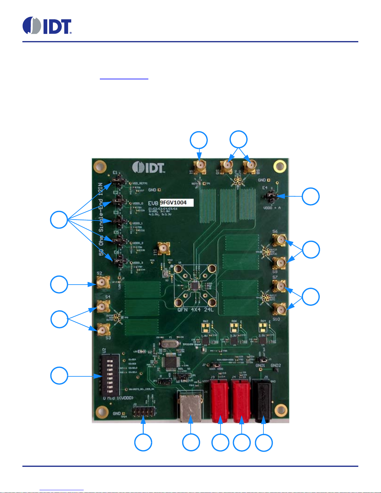
Use Figure 1 and Table 1 to identify: power supply jacks, USB connector, input and output frequency SMA connectors.
Figure 1. Evaluation Board Overview
™ software through USB, the device can be configured and programmed to generate
User Guide
1©2018 Integrated Device Technology, Inc. March 1, 2018
Page 2
9FGV1001, 9FGV1002, and 9FGV1004 PhiClock™ PCIe Evaluation Board User Guide
Table 1. Evaluation Board Pins and Functions
Label Number Name On-board Connector Label Function
2
1I
C Interface Connector J2
Alternative I
IDT Timing Commander can also use Aardvark.
2
C interface connector for Aardvark.
Connect this USB to your PC to run IDT Timing
2 USB Connector J6
Commander.
The board can be powered from the USB port.
3 Output Power Supply Jack J3
4 Core Power Supply Jack J4
Connect to 1.8V, 2.5V or 3.3V for the output voltage of
the device.
Connect to 1.8V, 2.5V or 3.3V for the core voltage of the
device.
5 Ground Jack J5 Connect to ground of power supply.
6 Differential Output 1 S7 and S10
7 Differential Output 2 S6 and S9
8 Differential Output 3 S5 and S8
Can be a differential pair, or two single-ended outputs.
Available logic types: LVCMOS, LVDS and LP-HCSL.
Can be a differential pair, or two single-ended outputs.
Available logic types: LVCMOS, LVDS and LP-HCSL.
Can be a differential pair, or two single-ended outputs.
Available logic types: LVCMOS, LVDS and LP-HCSL.
9 Reference Output 0 S1 Reference or buffered output from the crystal.
VDD_REFP1, VDDO_0, VDDO_1, four-way headers
10
Power Supply Voltage
Selector
E1, E2, E3, E4, E5, E6
used to select a power supply voltage. Connect the
center pin to one of the 4 surrounding pins to select a
voltage or a source.
11 Reference Output 1 S2 Reference or buffered output from the crystal.
12 Differential Output 0 S3 and S4
Can be a differential pair, or two single-ended outputs.
Available logic types: LVCMOS, LVDS and LP-HCSL.
13 DIP Switch U2
Board Power Supply
The evaluation board uses jumpers E1–E6 to set the power supply voltages for various VDD pins. The 4-way jumpers can select 3
different voltages from regulators that use power from the USB port. Selection #2 is the jack for connecting a bench power supply.
E1: Power supply for the REF outputs. The E1 voltage also determines the LVCMOS output levels of the REF0 and REF1 outputs.
E2: Power supply for the OUT0 output driver.
E3: Power supply for the OUT1 output driver.
E4: Power supply for the analog (V
E5: Power supply for the OUT2 output driver.
E6: Power supply for the OUT3 output driver.
See 9FGV100x Evaluation Board Schematics (Figure 5–Figure 8) for detailed information.
DDA
) and digital (V
Used to control certain pins like OEA, OEB, SEL0, SEL1
2
and I
C versus Hardware Select mode.
) core VDD pins.
DDD
2©2018 Integrated Device Technology, Inc. March 1, 2018
Page 3

9FGV1001, 9FGV1002, and 9FGV1004 PhiClock™ PCIe Evaluation Board User Guide
DIP Switch (U2)
Refer to Figure 2 and Table 2 for the DIP switch settings and functions.
Figure 2. DIP Switch (U2)
Table 2. DIP Switch Settings
Switch Number Function
1 = OEA
See datasheet.
2 = OEB
3 = SEL0
Select 1 of 4 pre-programmed configurations when in Hardware Select mode. Also see switch 8.
4 = SEL1
5 Not used.
6 Not used.
7 Not used.
Selects operating mode at power-up.
2
8 = Mode
“-” or “O” selects I
C mode.
“+” selects Hardware Select mode.
Interfacing with a Computer to Run Timing Commander
As shown in Figure 3, jumpers JP1 and JP2 are installed to use the FTDI chip U6 for connecting to the computer with the USB port J6.
The U6 chip translates USB to I
When using Aardvark, remove jumpers JP1 and JP2 and connect the Aardvark to connector J2. Default I
9FGV100x is 0x68.
2
C.
2
C device address for the
Miscellaneous interfaces can connect to J2 pin 1 for the Serial Clock and to J2 pin 3 for the Serial Data signal. J2 pin 2 can be used as
ground, but any other ground pin will also work.
When OTP in the 9FGV100x devices is burned with multiple configurations, JP1 and JP2 can be applied in JP3 position respectively to
connect the SEL0 and SEL1 switches in U2. Move switch 8 to “+” and power-up the 9FGV100x in Hardware Select mode. This enables
changing between 4 configurations with SEL0/1.
3©2018 Integrated Device Technology, Inc. March 1, 2018
Page 4

9FGV1001, 9FGV1002, and 9FGV1004 PhiClock™ PCIe Evaluation Board User Guide
Figure 3. Connecting to a Computer via USB Port J6
On-board Crystal
A 25MHz crystal is installed on the board and is used as the reference frequency. The board can also be modified to insert an external
reference clock into the XIN pin using SMA connector S11. When using an external reference clock, additional components need to be
assembled and the crystal needs to be removed.
Output Terminations
Each differential output has a pair of SMA connectors to connect to a 50Ω coax. It is recommended to combine the two signals using a
balun or splitter/combiner device when measuring jitter or phase noise. The circuit at the SMA connectors is shown in Figure 4.
Figure 4. SMA Connectors Circuit
4©2018 Integrated Device Technology, Inc. March 1, 2018
Page 5

9FGV1001, 9FGV1002, and 9FGV1004 PhiClock™ PCIe Evaluation Board User Guide
The circuit is designed for maximum flexibility when testing all possible logic types. Default assembly uses a 0.1μF capacitor in place of
R14 and R16, and the short across R14 and R16 is cut. No other devices are assembled. This simple AC-coupled configuration allows for
testing phase noise and jitter of all possible logic types. The circuit can be modified for custom tests. TP3 is a position to place a
differential FET probe.
Operating Instructions
1. Set all jumpers for power supply choices (E1–E6), interface choices (JP1 and JP2), and set the U2 switches.
2. Connect an interface: USB or I
2
C.
3. In the case of an I2C interface, also connect external power supply to jacks J3, J4 and J5.
4. Start Timing Commander for either USB or Aardvark.
a. Start new configuration or load TCS file for existing configuration.
b. Choose PhiClock personality.
c. For Aardvark, click to select Aardvark “Connection Interface”.
d. For a new configuration, prepare all settings.
e. Click to connect to the 9FGV100x device. Top right should turn green.
f. Click to write all settings to the 9FGV100x device.
g. It should now be possible to measure clocks on outputs.
h. While connected, each change to the settings will be written to the 9FGV100x immediately and can be observed at the clock outputs.
5©2018 Integrated Device Technology, Inc. March 1, 2018
Page 6

Schematics
5
5
4
4
3
3
2
2
1
1
D D
C C
B B
A A
9FGS9091/9FGV1001/9FGV1004
SE Trace 12 inches/50ohm
SE Trace 12 inches/50ohm
SE Trace 12 inches/50ohm
SE Trace 12 inches/50ohm
SE Trace 12 inches/50ohm
SE Trace 12 inches/50ohm
SE Trace 12 inches/50ohm
SE Trace 12 inches/50ohm
SE Trace 12 inches/50ohm
Support LVCMOS/PCIEX/LVDS
Support LVCMOS/PCIEX/LVDS
cut-able trace
cut-able trace option:
1) Use SMA: don't cut; no load cap
2) No SMA: cut
SE Trace 12 inches/50ohm
OUT0T
OUT0C
OUT1T
OUT1C
OUT2T
OUT2C
VDDAp
VDDO3
VDDO1
VDDO0
VDDREFp
GND
VDDO2
VDDDp
GND
VDDDp
GND
GND
GND
GND
GND
GND
GND
GND
GND
GND
GND
GND
GND
GND
GND
GND
GND
XO
{2}
XIN_CLKIN
{2}
SEL1_SDA{2}
SEL0_SCL{2}
OE_B{2}
vREF0_SEL_I2CB_SW{2}
OE_A
{2}
Title
Size Document Number Rev
Date: Sheet
of
1
9FGS9091 EVB revB
B
14Tuesday, August 16, 2016
Title
Size Document Number Rev
Date: Sheet
of
1
9FGS9091 EVB revB
B
14Tuesday, August 16, 2016
Title
Size Document Number Rev
Date: Sheet
of
1
9FGS9091 EVB revB
B
14Tuesday, August 16, 2016
S7
1
2
345
1
2
R17
0 _NP
TP6
IO22IO4
4
GND11GND3
3
R56
50_NP
12
TP3
IO22IO4
4
GND11GND3
3
1
2
C4
2pF_NP
R60
50_NP
12
S1
1
2
345
R21
50_NP
12
1
2
C3
2pF_NP
1
2
R7
0 _NP
1
2
R25
0 _NP
1
2
C6
2pF_NP
R57
50_NP
12
1
2
R1
0 _NP
R61
50_NP
12
1
2
C1
5pF_NP
1
2
C5
2pF_NP
S9
1
2
345
S4
1
2
345
R8 0
12
TP1
REF0
IO1GND
2
1
2
C10
2pF_NP
S3
1
2
345
1
2
C2
5pF_NP
S6
1
2
345
R12 0
1 2
S8
1
2
345
R4 33
1 2
TP5
IO22IO4
4
GND11GND3
3
S5
1
2
345
R2 10K
1 2
R5 0
12
R58
50_NP
12
TP4
IO22IO4
4
GND11GND3
3
R20
50_NP
12
1
2
R19
0 _NP
TP2
REF1
IO1GND
2
1
2
R24
0 _NP
S2
1
2
345
U1
9FGS9091_24NBG
REF13SEL0/SCL
4
XIN/CLKI N1XO
2
OEA6OEB
8
OTP_VPP
9
VDDDp
7
SEL1/SDA
5
VDDAp
22
VDDREFp
24
VDDO3
21
vREF0_SEL_I2CB
23
OUT3
20
OUT3B
19
VDDO2
18
OUT2
17
OUT2B
16
VDDO1
15
OUT1
14
OUT1B13OUT0B
10
OUT0
11
VDDO0
12
EPAD1
25
EPAD2
26
EPAD3
27
EPAD4
28
EPAD5
29
EPAD6
30
EPAD7
31
EPAD8
32
EPAD9
33
R10 0
1 2
R13 0
1 2
S10
1
2
345
R54
50_NP
12
R59
50_NP
12
1
2
C7
2pF_NP
1
2
R23
0 _NP
R9 0
12
R22
50_NP
12
1
2
C9
2pF_NP
R3
33
1 2
1
2
J1
HEADER 2
1
2
R16
0 _NP
1
2
C8
2pF_NP
1
2
R14
0 _NP
R11 0
1 2
R6 0
12
R15
50_NP
12
1
2
R18
0 _NP
R55
50_NP
12
OUT2T
OUT2C
vREF0_SEL_I2CB
XOp2
SEL1_SDA
vREF0_SEL_I2CB
OUT0T
OUT0C
OUT1T
OUT1C
vREF0_SEL_I2CB_SW
VDDO3p21
VDDO0p12
OUT1B
OUT1
VDDO1p15
VDDREFp24
OUT0B
OUT0
VDDAp22
VDDO2p18
OEB
REF1
OUT0T
OUT0C
OUT1T
OUT1C
OUT3T
OUT3C
OEA
SEL0_SCL
VDDDp7
XIN_CLKINp1
REF1
OUT2T
OUT2B
OUT3C
OUT3
OUT2
OUT3B
OUT2C
OUT3T
OTP_VPP
REF0p23
REF1p3
REF0_S
REF1_S
O0C_S
O0T_S
O1C_S
O1T_S
O2C_S
O2T_S
O3C_S
O3T_S
CM0
CM1
CM2
CM3
Figure 5. 9FGV100x Evaluation Board Schematic – page 1
9FGV1001, 9FGV1002, and 9FGV1004 PhiClock™ PCIe Evaluation Board User Guide
6©2018 Integrated Device Technology, Inc. March 1, 2018
Page 7

9FGV1001, 9FGV1002, and 9FGV1004 PhiClock™ PCIe Evaluation Board User Guide
5
5
4
4
3
3
2
2
1
1
D D
C C
B B
A A
LABEL:
OEB
SEL0
SEL1
SEL[1:0]/I2C (Float)
AADVARK
Unpopulate C23 when Crystal is used as
input reference
Overlap C23 XIN_CLKIN with C21 XIN_CLKIN
I2C
I2C HW SEL
HW SEL
OEA
ESR resistor test
cut-able trace
VDDDp
VDDDp
GND
GND
GND
GND
GND
GND
GND
GND
SEL0 {1,2}
SEL1 {1,2}
OE_B {1}
XIN_CLKIN
{1}
XO {1}
vREF0_SEL_I2CB_SW {1}
SEL0_SCL {1}
SEL1_SDA {1}
SDA {2,4}
SCL {2,4}
SEL1
{1,2}
SEL0 {1,2}
OE_A
{1}
Title
Size Document Number Rev
Date: Sheet
of
1
9FGS9091 EVB revB
B
24Tuesday, August 16, 2016
Title
Size Document Number Rev
Date: Sheet of
1
9FGS9091 EVB revB
B
24Tuesday, August 16, 2016
Title
Size Document Number Rev
Date: Sheet of
1
9FGS9091 EVB revB
B
24Tuesday, August 16, 2016
J2
AARDVARK HEADER 5X2
246810
13579
R27 10K
1 2
R29 50_NP
1 2
R31 0
1 2
R33
1K
12
TP22
1
JP1
HEADER 3
1
2
3
TP21
1
S11
SMA STRAIGHT_NP
1
2
345
C13
100pF _NP
12
JP2
HEADER 3
1
2
3
R28 10K
1 2
U2
DIP_SW8
VCC
1
VEE
8
s89s710s611s512s413s314s215s1
16
C11
6.8pF_NP
12
C12
6.8pF_NP
12
R26
0_NP
1 2
X1
25MHz
1
3
2 4
R32
1K
12
LD1
Green
R30 0
1 2
OEB
XIN_CLKIN_X1
SEL0
SEL1SELR1
R30_LED
XINRCONN
XIN_CLKIN_X1
SEL1_SDA
XO_X2
SELR0
OEA
XO_R
cut-able
SCL_AADVAR
SDA_AADVAR
Figure 6. 9FGV100x Evaluation Board Schematic – page 2
7©2018 Integrated Device Technology, Inc. March 1, 2018
Page 8

9FGV1001, 9FGV1002, and 9FGV1004 PhiClock™ PCIe Evaluation Board User Guide
5
5
4
4
3
3
2
2
1
1
D D
C C
B B
A A
Locate near
DUT power pin
LABEL ON EACH RESPECTIVE PIN OF
HEADERS: 1.8V, 2.5V, 3.3V
Header Alignment:
Single pin header above
and below the center pin
of 3-pin header so that
center pin can be jumped
with the surrounding 4
pins, shown as left
Locate near
DUT power pin
VDDO_J
GND GND
GND
VDD_J VDDAp
VDDDp
GND GND
GND
GND
VDDREFp
VDDO0
VDDO1
GND
GND
GNDGND
GND
GND
GND
GND
VDDO3
GNDGND
VDDO2
GNDGND
GND
GND
GND
GND
GND
GND
USB_5V {3,4}
Title
Size Document Number Rev
Date: Sheet
of
1
9FGS9091 EVB REVB
B
34Tuesday, August 16, 2016
Title
Size Document Number Rev
Date: Sheet of
1
9FGS9091 EVB REVB
B
34Tuesday, August 16, 2016
Title
Size Document Number Rev
Date: Sheet of
1
9FGS9091 EVB REVB
B
34Tuesday, August 16, 2016
FB2
600 ohm 500mA
21
VDDO_2
C40
0.01uF
12
R66
POT_25K_NP
1 3
2
FB1
600 ohm 500mA
21
E6
325
4
1
J4
Power Jack Red
C17
10uF
R38 15K_1%
1 2
R63
1K_NP
1 2
C20
10uF
C34
0.1uF
12
C18
0.1uF
12
C25
0.1uF
12
FB3
600 ohm 500mA
21
C46
0.1uF
12
VDDO_3
C28
0.1uF
12
J5
Power Jack Black
R64
POT_25K_NP
1 3
2
R67
1K_NP
1 2
FB4
600 ohm 500mA
21
C36
0.1uF
12
C44
10uF
C47
10uF
C37
0.01uF
12
C26
10uF
C31
0.1uF
12
C14
0.1uF
12
GND2
C22
0.1uF
12
FB6
600 ohm 500mA
21
1
2
J7
HEADER 2
R65
1K_NP
1 2
C43
0.1uF
12
VDDAP_VDDDP1
C41
10uF
E1
325
4
1
C27
0.1uF
12
C21
0.1uF
12
VDDO_4
C30
0.1uF
12
C15
10uF
U3
LP38789
IN1IN2IN(CP)3CP4EN5GND(CP)
6
GND
7
FB
8
SET
9
OUT(FB)
10
OUT11OUT
12
EPAD
13
EPAD
14
EPAD
15
EPAD
16
EPAD
17
EPAD
18
EPAD
19
EPAD
20
EPAD
21
C32
10uF
FB5
600 ohm 500mA
21
R62
POT_25K_NP
1 3
2
GND1
C23
10uF
C45
0.1uF
12
R35
10.5K_1%
12
C19
0.1uF
12
E2
325
4
1
E5
325
4
1
C33
0.1uF
12
E3
325
4
1
C16
0.1uF
12
U4
LP38789
IN1IN2IN(CP)3CP4EN5GND(CP)
6
GND
7
FB
8
SET
9
OUT(FB)
10
OUT11OUT
12
EPAD
13
EPAD
14
EPAD
15
EPAD
16
EPAD
17
EPAD
18
EPAD
19
EPAD
20
EPAD
21
C48
10uF
R39
23.2K_1%
12
VDDO_1
C39
10uF
FB7
600 ohm 500mA
21
VDD_REFP1
J3
Power Jack Red
R34 2.2
1 2
C29
10uF
C42
10uF
C24
0.1uF
12
U5
LP38789
IN1IN2IN(CP)3CP4EN5GND(CP)
6
GND
7
FB
8
SET
9
OUT(FB)
10
OUT11OUT
12
EPAD
13
EPAD
14
EPAD
15
EPAD
16
EPAD
17
EPAD
18
EPAD
19
EPAD
20
EPAD
21
C38
10uF
R36 21K_1%
1 2
R40 13.3K_1%
1 2
R37
16.2K_1%
12
E4
325
4
1
C35
10uF
VDDO_J
VDDO_J
VDDO_J
GND_J
VDD_J R31_C31
USB_5V VDDO_1.8V
VDDO_1
VDD_REFp
VDDO_0
USB_5V
R32_C45
USB_5V
R33_C48
USB_5V VDDO_3.3V
R36_C56
GND
VDDO_2.5V
VDDO_3.3V
VDDO_1.8V
VDDO_2.5V
VDDO_3.3V
VDDO_1.8V
VDDO_2.5V
VDDO_3.3V
VDDO_1.8V
VDDO_2.5V
VDDO_3.3V
VDDO_1.8V
VDDO_3
VDDO_2.5V
VDDO_2.5V
VDDO_3.3V
VDDO_1.8V
VDDO_2
VDDO_J
VDDO_J
VDDO_2.5V
VDDO_3.3V
VDDO_1.8V
VDDA_VDDD
VDDA_p
REG_CP3
REG_SET3
REG_D3
REG_CP4
REG_SET4
REG_D4
REG_CP5
REG_SET5
REG_D5
Figure 7. 9FGV100x Evaluation Board Schematic – page 3
8©2018 Integrated Device Technology, Inc. March 1, 2018
Page 9

9FGV1001, 9FGV1002, and 9FGV1004 PhiClock™ PCIe Evaluation Board User Guide
5
5
4
4
3
3
2
2
1
1
D D
C C
B B
A A
On Layout, make EPAD to easy connect to GND
mod1: connect C55 p1 to C52 p1
TP23: Label TP23 / 5V INPUT
R41: provide USB 5 V to Regulators
GND
VCC2232_3V
GND
GND
GND
GND
GND
GND
GND
GND
SDA {2}
SCL {2}
USB_5V{3}
Title
Size Document Number Rev
Date: Sheet
of
1
IDT_9FGS9091 EVM_BOARD_REV1
B
44Tuesday, August 16, 2016
Title
Size Document Number Rev
Date: Sheet
of
1
IDT_9FGS9091 EVM_BOARD_REV1
B
44Tuesday, August 16, 2016
Title
Size Document Number Rev
Date: Sheet
of
1
IDT_9FGS9091 EVM_BOARD_REV1
B
44Tuesday, August 16, 2016
C56
0.1uF
12
R41
0
1 2
R51
10K
1 2
R47 0
1 2
R44
27
12
R48
1.5K
1 2
TP24
C53
47uF
C805A
12
U6
FT2232_LQFP48
EESK1EEDATA
2
VCC
3
RESET#
4
RSTOUT#
5
3V3OUT
6
USBDP7USBDM
8
GND
9
SI/WUA
10
GPIOH311GPIOH212GPIOH1
13
VCCIOA
14
GPIOH0
15
GPIOL316GPIOL2
17
GND
18
GPIOL119GPIOL0
20
TMS/CS
21
TDO/DI22TDI/DO
23
TCK/SK
24
GND
25
SI/WUB
26
UNUSED1127UNUSED10
28
UNUSED929UNUSED8
30
VCCIOB
31
UNUSED732UNUSED6
33
GND
34
UNUSED535UNUSED436UNUSED337UNUSED238UNUSED139UNUSED0
40
PWREN#
41
VCC
42
XTIN
43
XTOUT
44
AGND
45
AVCC
46
TEST
47
EECS
48
EPAD1
49
EPAD2
50
EPAD3
51
EPAD4
52
R43
470
12
TP23
FB8
300ohm 2A
2 1
J6
USB PORT
VBUS
1
D-
2
D+
3
GND
4
C57
0.1uF
12
Y1
6MHz
12
C50 0.1uF
1 2
C54 10uF
C49 10nF
1 2
C51 0.1uF
1 2
C58
33pF
1
2
C52 10uF
FB9
600 ohm 500mA
21
C55
0.1uF
1 2
R46 0
1 2
R49
10K
1 2
LD2
Green
C59
33pF
R45
27
12
FB10
300ohm 2A
2 1
R50
10K
12
R42
1K
12
USB_9
3V3_USB
3V3_USB0
3V3_USB1
3V3_USB
XTIN
VCC2232
USB_15
3V3_USB
USB_6
USB_5
USB_4
USB_7
VCC2232
USB_10
XTOUT
USB_13
USB_3
USB_14
USB_12
USB_2
USB_8
USB_1
USB_11
Figure 8. 9FGV100x Evaluation Board Schematic – page 4
9©2018 Integrated Device Technology, Inc. March 1, 2018
Page 10

9FGV1001, 9FGV1002, and 9FGV1004 PhiClock™ PCIe Evaluation Board User Guide
Ordering Information
Orderable Part Number Description
EVK9FGV1001
Evaluation board with all differential outputs AC coupled.EVK9FGV1002
EVK9FGV1004
Revision History
Revision Date Description of Change
March 1, 2018 Initial release.
Corporate Headquarters
6024 Silver Creek Valley Road
San Jose, CA 95138 USA
www.IDT.com
DISCLAIMER Integrated Device Technology, Inc. (IDT) and its affiliated companies (herein referred to as “IDT”) reserve the right to modify the products and/or specifications described herein at any time,
without notice, at IDT’s sole discretion. Performance specifications and operating parameters of the described products are determined in an independent state and are not guaranteed to perform the same
way when installed in customer products. The information contained herein is provided without representation or warranty of any kind, whether express or implied, including, but not limited to, the suitability
of IDT's products for any particular purpose, an implied warranty of merchantability, or non-infringement of the intellectual property rights of others. This document is presented only as a guide and does not
convey any license under intellectual property rights of IDT or any third parties.
IDT's products are not intended for use in applications involving extreme environmental conditions or in life support systems or similar devices where the failure or malfunction of an IDT product can be reasonably expected to significantly affect the health or safety of users. Anyone using an IDT product in such a manner does so at their own risk, absent an express, written agreement by IDT.
Integrated Device Technology, IDT and the IDT logo are trademarks or registered trademarks of IDT and its subsidiaries in the United States and other countries. Other trademarks used herein are the property
of IDT or their respective third party owners. For datasheet type definitions and a glossary of common terms, visit www.idt.com/go/glossary. Integrated Device Technology, Inc.. All rights reserved.
Sales
1-800-345-7015 or 408-284-8200
Tech Support
www.IDT.com/go/support
Fax: 408-284-2775
www.IDT.com/go/sales
10©2018 Integrated Device Technology, Inc. March 1, 2018
Page 11

Mouser Electronics
Authorized Distributor
Click to View Pricing, Inventory, Delivery & Lifecycle Information:
IDT (Integrated Device Technology):
EVK9FGV1001 EVK9FGV1004 EVK9FGV1002 EVK9FGV1001Q5 EVK9FGV1002Q5 EVK9FGV1004Q5
 Loading...