

Page 1

®
Tsi381
™
Evaluation Board User Manual
60E2000_MA001_03
September 2009
6024 Silver Creek Valley Road, San Jose, California 95138
Telephone: (800) 345-7015 • (408) 284-8200 • FAX: (408) 284-2775
©2009 Integrated Device Technology, Inc.
Printed in U.S.A.
Page 2

Integrated Device Technology, Inc. reserves the right to make changes to its products or specifications at any time, without notice, in order to improve design or performance
and to supply the best possible product. IDT does not assume any responsibility for use of any circuitry described other than the circuitry embodied in an IDT product. The
Company makes no representations that circuitry described herein is free from patent infringement or other rights of third parties which may result from its use. No license is
granted by implication or otherwise under any patent, patent rights or other rights, of Integrated Device Technology, Inc.
GENERAL DISCLAIMER
Code examples provided by IDT are for illustrative purposes only and should not be relied upon for developing applications. Any use of the code examples below is completely
at your own risk. IDT MAKES NO REPRESENT ATIONS OR WARRANTIES OF ANY KIND CONCERNING THE NONINFRINGEMENT, QUALITY, SAFETY OR SUITABILITY
OF THE CODE, EITHER EXPRESS OR IMPLIED, INCLUDING WITHOUT LIMITATION ANY IMPLIED WARRANTIES OF MERCHANTABILITY, FITNESS FOR A PARTICULAR PURPOSE, OR NON-INFRINGEMENT. FURTHER, IDT MAKES NO REPRESENT ATIONS OR WARRANTIES AS TO THE TRUTH, ACCURACY OR COMPLETENESS
OF ANY STATEMENTS, INFORMATION OR MATERIALS CONCERNING CODE EXAMPLES CONTAINED IN ANY IDT PUBLICATION OR PUBLIC DISCLOSURE OR
THAT IS CONTAINED ON ANY IDT INTERNET SITE. IN NO EVENT WILL IDT BE LIABLE FOR ANY DIRECT, CONSEQUENTIAL, I NCIDENTAL, INDIRECT, PUNITIVE OR
SPECIAL DAMAGES, HOWEVER THEY MAY ARIS E, AND EVEN IF IDT HAS BEEN PREVIOUSLY ADVISED ABOUT THE POSSIBILITY OF SUCH DAMAGES. The code
examples also may be subject to United States export control laws and may be subject to the export or import laws of other countries and it is your responsibility to comply with
any applicable laws or regulations.
Integrated Device Technology's products are not authorized for use as critical components in life support devices or systems unless a specific written agreement pertaining to
such intended use is executed between the manufacturer and an officer of IDT.
1. Life support devices or systems are devices or systems which (a) are intended for surgical implant into the body or (b) support or sustain life and whose failure to perform,
when properly used in accordance with instructions for use provided in the labeling, can be reasonably expected to result in a significant injury to the user.
2. A critical component is any components of a life support device or system whose failure to perform can be reasonably expected to cause the failure of the life support device
or system, or to affect its safety or effectiveness.
IDT, the IDT logo, and Integrated Device Technology are trademarks or registered trademarks of Integrated Device Technology, Inc.
CODE DISCLAIMER
LIFE SUPPORT POLICY
Page 3

Contents
About this Document. . . . . . . . . . . . . . . . . . . . . . . . . . . . . . . . . . . . . . . . . . . . . . . . . . . . . 5
Related Information . . . . . . . . . . . . . . . . . . . . . . . . . . . . . . . . . . . . . . . . . . . . . . . . . . . . . . . . . . . . . . . . . . . . . . . . . . . . . . 5
Acronyms . . . . . . . . . . . . . . . . . . . . . . . . . . . . . . . . . . . . . . . . . . . . . . . . . . . . . . . . . . . . . . . . . . . . . . . . . . . . . . . . . . . . . . 5
Revision History . . . . . . . . . . . . . . . . . . . . . . . . . . . . . . . . . . . . . . . . . . . . . . . . . . . . . . . . . . . . . . . . . . . . . . . . . . . . . . . . . 5
1. Board Design . . . . . . . . . . . . . . . . . . . . . . . . . . . . . . . . . . . . . . . . . . . . . . . . . . . . . . . 7
1.1 Overview . . . . . . . . . . . . . . . . . . . . . . . . . . . . . . . . . . . . . . . . . . . . . . . . . . . . . . . . . . . . . . . . . . . . . . . . . . . . . . . . . 7
1.2 PCI Interface . . . . . . . . . . . . . . . . . . . . . . . . . . . . . . . . . . . . . . . . . . . . . . . . . . . . . . . . . . . . . . . . . . . . . . . . . . . . . . 9
1.2.1 Overview . . . . . . . . . . . . . . . . . . . . . . . . . . . . . . . . . . . . . . . . . . . . . . . . . . . . . . . . . . . . . . . . . . . . . . . . . 9
1.2.2 IDSEL Signals . . . . . . . . . . . . . . . . . . . . . . . . . . . . . . . . . . . . . . . . . . . . . . . . . . . . . . . . . . . . . . . . . . . . . 9
1.2.3 Interrupt Signals. . . . . . . . . . . . . . . . . . . . . . . . . . . . . . . . . . . . . . . . . . . . . . . . . . . . . . . . . . . . . . . . . . . . 9
1.2.4 Pull-up Signals. . . . . . . . . . . . . . . . . . . . . . . . . . . . . . . . . . . . . . . . . . . . . . . . . . . . . . . . . . . . . . . . . . . . . 9
1.3 PCIe Interface. . . . . . . . . . . . . . . . . . . . . . . . . . . . . . . . . . . . . . . . . . . . . . . . . . . . . . . . . . . . . . . . . . . . . . . . . . . . . 10
1.4 Power Management . . . . . . . . . . . . . . . . . . . . . . . . . . . . . . . . . . . . . . . . . . . . . . . . . . . . . . . . . . . . . . . . . . . . . . . . 10
1.4.1 Power Regulation. . . . . . . . . . . . . . . . . . . . . . . . . . . . . . . . . . . . . . . . . . . . . . . . . . . . . . . . . . . . . . . . . . 10
1.4.2 Power Requirements . . . . . . . . . . . . . . . . . . . . . . . . . . . . . . . . . . . . . . . . . . . . . . . . . . . . . . . . . . . . . . . 11
1.4.3 Power Sequencing . . . . . . . . . . . . . . . . . . . . . . . . . . . . . . . . . . . . . . . . . . . . . . . . . . . . . . . . . . . . . . . . . 13
1.4.4 System Power Design . . . . . . . . . . . . . . . . . . . . . . . . . . . . . . . . . . . . . . . . . . . . . . . . . . . . . . . . . . . . . . 13
1.4.5 PCI Vaux (PCI Auxiliary) Support . . . . . . . . . . . . . . . . . . . . . . . . . . . . . . . . . . . . . . . . . . . . . . . . . . . . 14
1.5 Clock Management . . . . . . . . . . . . . . . . . . . . . . . . . . . . . . . . . . . . . . . . . . . . . . . . . . . . . . . . . . . . . . . . . . . . . . . . 14
1.5.1 PCI . . . . . . . . . . . . . . . . . . . . . . . . . . . . . . . . . . . . . . . . . . . . . . . . . . . . . . . . . . . . . . . . . . . . . . . . . . . . . 14
1.5.2 System Clock Distribution. . . . . . . . . . . . . . . . . . . . . . . . . . . . . . . . . . . . . . . . . . . . . . . . . . . . . . . . . . . 15
1.6 Other Interfaces . . . . . . . . . . . . . . . . . . . . . . . . . . . . . . . . . . . . . . . . . . . . . . . . . . . . . . . . . . . . . . . . . . . . . . . . . . . 15
1.6.1 JTAG Interface. . . . . . . . . . . . . . . . . . . . . . . . . . . . . . . . . . . . . . . . . . . . . . . . . . . . . . . . . . . . . . . . . . . . 15
1.6.2 EEPROM Interface . . . . . . . . . . . . . . . . . . . . . . . . . . . . . . . . . . . . . . . . . . . . . . . . . . . . . . . . . . . . . . . . 15
1.6.3 GPIO Interface. . . . . . . . . . . . . . . . . . . . . . . . . . . . . . . . . . . . . . . . . . . . . . . . . . . . . . . . . . . . . . . . . . . . 16
1.7 Hardware Reset . . . . . . . . . . . . . . . . . . . . . . . . . . . . . . . . . . . . . . . . . . . . . . . . . . . . . . . . . . . . . . . . . . . . . . . . . . . 16
1.8 Logic Analyzer Connectivity . . . . . . . . . . . . . . . . . . . . . . . . . . . . . . . . . . . . . . . . . . . . . . . . . . . . . . . . . . . . . . . . . 17
3
2. Configurable Options. . . . . . . . . . . . . . . . . . . . . . . . . . . . . . . . . . . . . . . . . . . . . . . . 19
2.1 Switches . . . . . . . . . . . . . . . . . . . . . . . . . . . . . . . . . . . . . . . . . . . . . . . . . . . . . . . . . . . . . . . . . . . . . . . . . . . . . . . . . 19
2.1.1 DIP Switches . . . . . . . . . . . . . . . . . . . . . . . . . . . . . . . . . . . . . . . . . . . . . . . . . . . . . . . . . . . . . . . . . . . . . 19
2.1.2 Push Button . . . . . . . . . . . . . . . . . . . . . . . . . . . . . . . . . . . . . . . . . . . . . . . . . . . . . . . . . . . . . . . . . . . . . . 23
2.2 Shunt Jumpers . . . . . . . . . . . . . . . . . . . . . . . . . . . . . . . . . . . . . . . . . . . . . . . . . . . . . . . . . . . . . . . . . . . . . . . . . . . . 24
2.2.1 J6 Shunt Jumper. . . . . . . . . . . . . . . . . . . . . . . . . . . . . . . . . . . . . . . . . . . . . . . . . . . . . . . . . . . . . . . . . . . 25
2.2.2 J21 Shunt Jumper. . . . . . . . . . . . . . . . . . . . . . . . . . . . . . . . . . . . . . . . . . . . . . . . . . . . . . . . . . . . . . . . . . 25
2.3 Debug Headers. . . . . . . . . . . . . . . . . . . . . . . . . . . . . . . . . . . . . . . . . . . . . . . . . . . . . . . . . . . . . . . . . . . . . . . . . . . . 26
2.3.1 J22 Tsi381 JTAG . . . . . . . . . . . . . . . . . . . . . . . . . . . . . . . . . . . . . . . . . . . . . . . . . . . . . . . . . . . . . . . . . . 27
2.3.2 J23 Logic Analyzer PADs . . . . . . . . . . . . . . . . . . . . . . . . . . . . . . . . . . . . . . . . . . . . . . . . . . . . . . . . . . . 28
2.4 Connectors . . . . . . . . . . . . . . . . . . . . . . . . . . . . . . . . . . . . . . . . . . . . . . . . . . . . . . . . . . . . . . . . . . . . . . . . . . . . . . . 29
2.4.1 J1, J2, J36, J37 Connectors . . . . . . . . . . . . . . . . . . . . . . . . . . . . . . . . . . . . . . . . . . . . . . . . . . . . . . . . . . 30
2.4.2 J3 ATX Power Connector. . . . . . . . . . . . . . . . . . . . . . . . . . . . . . . . . . . . . . . . . . . . . . . . . . . . . . . . . . . . 30
Integrated Device Technology
www.idt.com
Tsi381 Evaluation Board User Manual
60E2000_MA001_03
Page 4

Contents4
2.4.3 P1 x1 PCIe Finger Connector . . . . . . . . . . . . . . . . . . . . . . . . . . . . . . . . . . . . . . . . . . . . . . . . . . . . . . . . 31
2.5 LEDs . . . . . . . . . . . . . . . . . . . . . . . . . . . . . . . . . . . . . . . . . . . . . . . . . . . . . . . . . . . . . . . . . . . . . . . . . . . . . . . . . . . 31
3. Bill of Materials . . . . . . . . . . . . . . . . . . . . . . . . . . . . . . . . . . . . . . . . . . . . . . . . . . . . .33
Tsi381 Evaluation Board User Manual
60E2000_MA001_03
Integrated Device Technology
www.idt.com
Page 5
About this Document
This document describes how to test the key features of the Tsi381 using the Tsi381 evaluation board.
It can be used in conjunction with the Tsi381 Evaluation Board Schematics.
Related Information
• Tsi381 User Manual
• Tsi381 Evaluation Board Schematics
• Tsi381 Board Design Guidelines
• PCI Express Base Specification (Revision 1.1)
• PCI Express CEM Specification (Revision 1.1)
• PCI Express-to-PCI/PCI-X Bridge Specification (Revision 1.0)
Acronyms
5
Term Definition
PCIe PCI Express
SerDes Serial/De-serializer
Revision History
60E2000_MA001_03, Formal, September 2009
This document was rebranded as IDT. It does not include any technical changes.
60E2000_MA001_02, Formal, September 2007
Added a new section that discusses “PCI Vaux (PCI Auxiliary) Support”.
60E2000_MA001_01, Formal, August 2007
This is the first version of the Tsi382 PCIe-to-PCI Bridge User Manual.
Integrated Device Technology
www.idt.com
Tsi381 Evaluation Board User Manual
60E2000_MA001_03
Page 6

About this Document6
Tsi381 Evaluation Board User Manual
60E2000_MA001_03
Integrated Device Technology
www.idt.com
Page 7

1. Board Design
Topics discussed include the following:
• “Overview” on page 7
• “PCI Interface” on page 9
• “PCIe Interface” on page 10
• “Power Management” on page 10
• “Clock Management” on page 14
• “Other Interfaces” on page 15
• “Hardware Reset” on page 16
• “Logic Analyzer Connectivity” on page 17
7
1.1 Overview
The key features of the Tsi381 evaluation board include the following (see also Figure 1):
• Single x1 lane, 2.5 Gbps PCIe 1.1 compatible riser card (extended height form factor)
• Four PCI slots
• 32-bit PCI bus, 25–66 MHz operation
• PCI power support through system or external supply
• PCIe compliance/debugging test points
Integrated Device Technology
www.idt.com
Tsi381 Evaluation Board User Manual
60E2000_MA001_03
Page 8
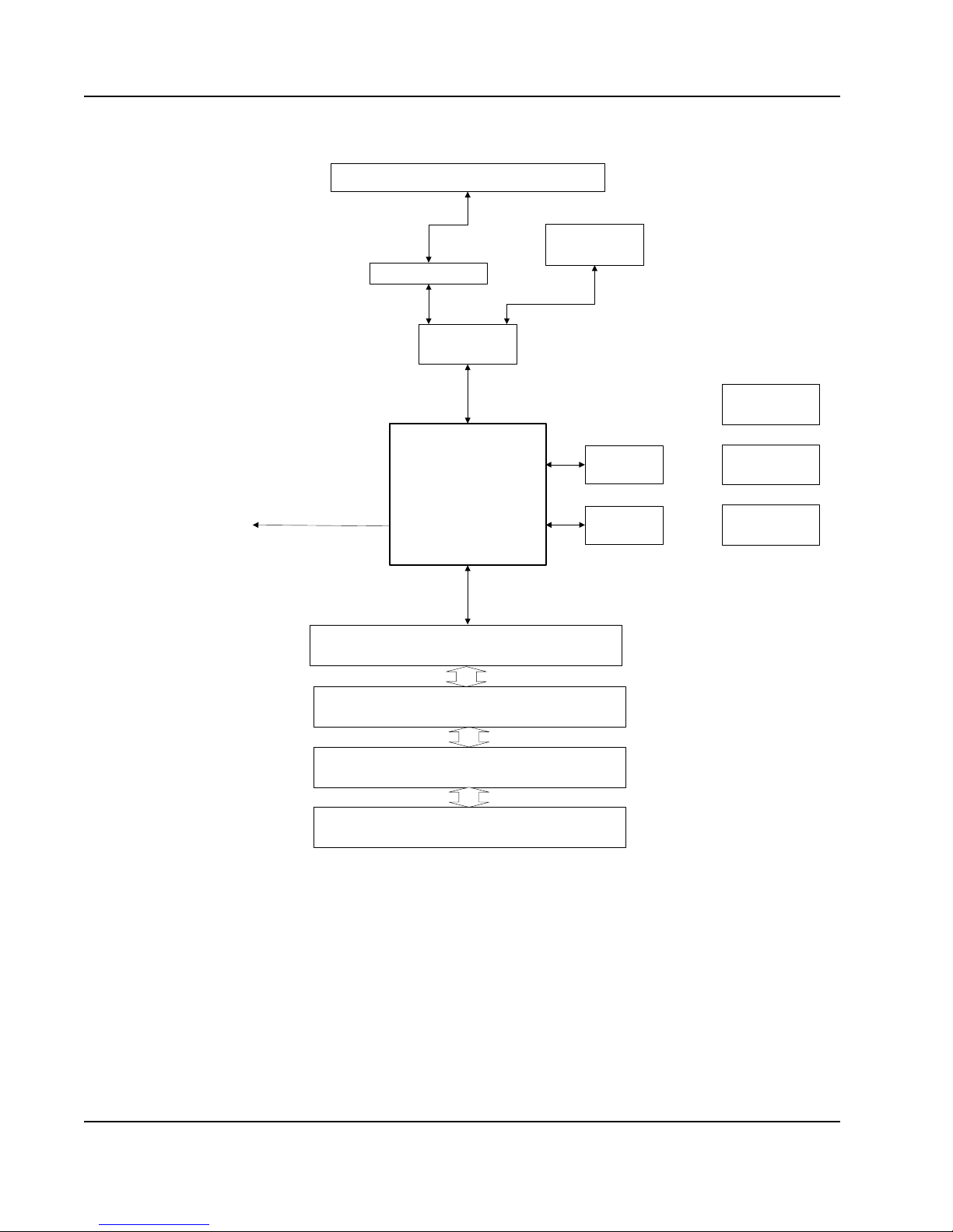
Figure 1: Evaluation Board Block Diagram
EEPROM
Tsi381
3.3V PCI 32-bit Connector
Slot 0
PCI
Power
Management
PCI Express Card Edge X1
PCIe
LA Probe
JTAG
Header
ATX Connectors
EEPROM
1x SerDes SMA
Points
SerDes Path
Resistor Select
Clock
Management
3.3V PCI 32-bit Connector
Slot 1
3.3V PCI 32-bit Connector
Slot 2
3.3V PCI 32-bit Connector
Slot 3
GPIO
GPIO
1. Board Design8
Tsi381 Evaluation Board User Manual
60E2000_MA001_03
Integrated Device Technology
www.idt.com
Page 9
1. Board Design 9
1.2 PCI Interface
1.2.1 Overview
The PCI Interface is implemented on the board with four slots, in which one is an R/A mounted
connector on the top of the board. All PCI connectors are compliant with the PCI 3.0 specification.
Appropriate clearance is provided such that up to four PCI cards can be inserted for testing while the
board is in an open-chassis standard ATX case.
The PCI Interface supports four slots operating at 25, 33, 50, or 66 MHz.
1.2.2 IDSEL Signals
IDSEL signals are connected in the following order:
• Slot 0 – R/A connector top slot: 150 ohms to AD16 (Device 0)
• Slot 1 – 150 ohms to AD17 (Device 1)
• Slot 2 – 150 ohms to AD19 (Device 3)
• Slot 3 – 150 ohms AD18 (Device 2)
1.2.3 Interrupt Signals
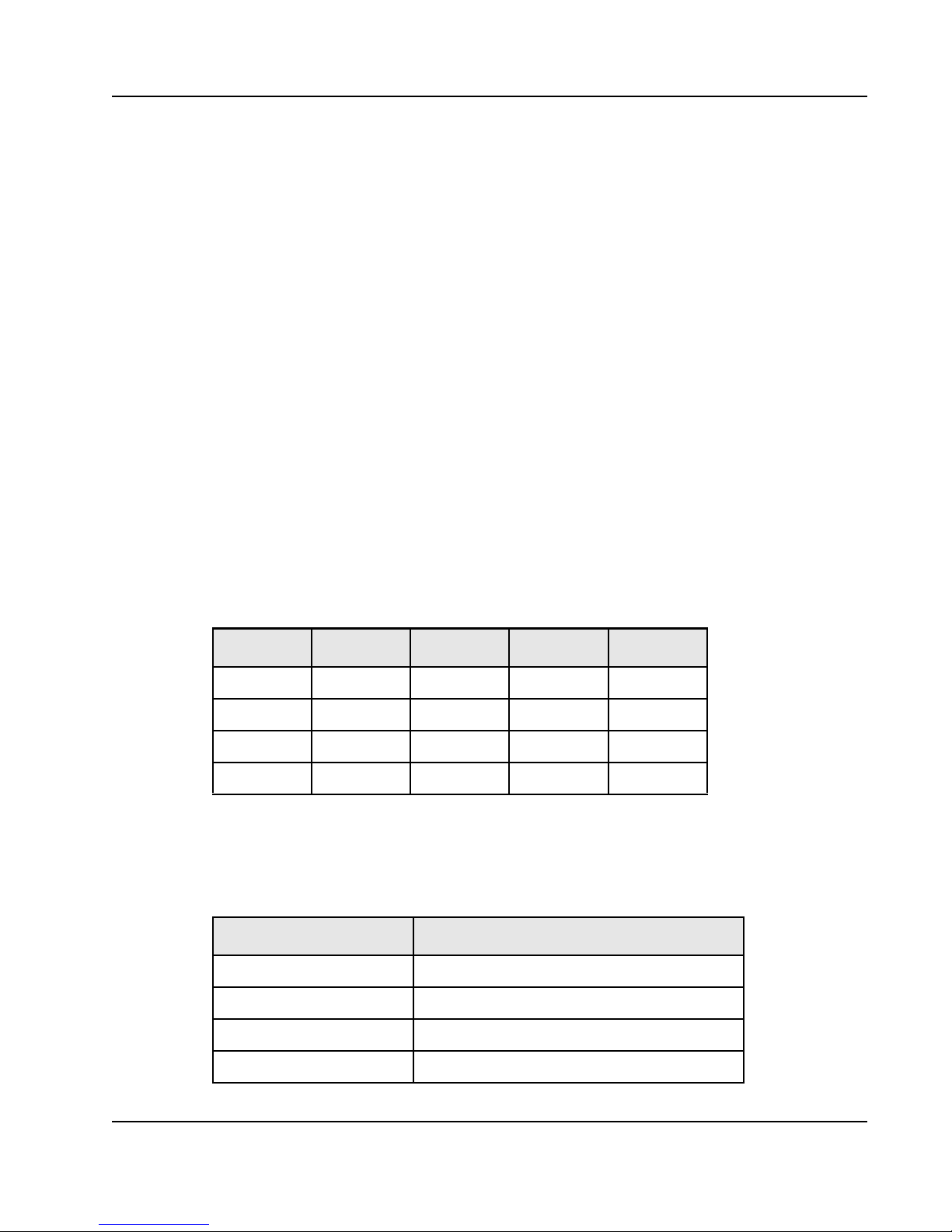
The PCI interrupt signals are connected to the slots as shown in the following table.
Table 1: PCI Interrupt Routing
Tsi381 Slot 0 Slot 1 Slot 3 Slot 4
AABDC
BBCAD
CCDBA
DDACB
1.2.4 Pull-up Signals
The following pull-ups are added to the PCI bus, in which a value of 8.2Kohm is used.
Table 2: PCI Pull-up Signals
Signal Description
PCI_REQ#[0:3] Bus request
PCI_GNT#[0:3] Bus grant
PCI_FRAME# Control signal
PCI_IRDY#, PCI_TRDY# Control signal
Integrated Device Technology
www.idt.com
Tsi381 Evaluation Board User Manual
60E2000_MA001_03
Page 10
Table 2: PCI Pull-up Signals (Continued)
Signal Description
PCI_STOP# Control signal
PCI_SERR# System error
PCI_PERR# Parity error
PCI_DEVSEL# Device select line
PCI_INT#[A:D] Interrupt line
PCI_PME# PCI Power Management Event occurred
1.3 PCIe Interface
The Tsi381 evaluation board implements a single lane PCIe Interface. It is designed to connect to a
PCIe system with a standard x1 finger connector. The system must provide the REFCLK and PERSTN
signals. The PCIe Interface has the following design elements:
1. Board Design10
• Supports Hot insertion and removal
• Mid-bus logic analyzer pads for PCIe RXD/TXD signal probing
• AC coupling on the TXD lanes
• JTAG TDI - TDO loopback for chain continuity
1.4 Power Management
1.4.1 Power Regulation
The evaluation board’s power regulation is implemented as follows:
• Digital 3.3V power supply available from DC/DC regulator or ATX supply
• Digital 1.2V switching regulator
• PCIe supplies filtered using EMI ferrite networks
To support PCI cards, the following additional power resources are included:
• 12V to 5V DC/DC converter
• 12V to 3.3V DC/DC converter
• External power connectors – ATX 20-pin connector for supplying all power from an ATX power
supply
Tsi381 Evaluation Board User Manual
60E2000_MA001_03
Integrated Device Technology
www.idt.com
Page 11
1. Board Design 11
1.4.2 Power Requirements
The power requirements and implementation for the Tsi381 is as follows.
Table 3: Tsi381 Power Requirements
Supply Name Symbol Supplied Source
Device Core 1.2V_384 DC/DC switching regulator w/Enable pin
PCIe 1.2V Core 1.2V_A_384 Passive Filter
PCI 3.3V supply 3.3V_384 Power switch w optional Ferrite filter to reduce
EMI/noise from PCI environment
PCIe 3.3V supply 3.3V_A_384 Passive Filter
The target power draw of the Tsi381 is a maximum of 1W, all supplies combined. The supplies to the
Tsi381 are controlled during ramp up using enable pins on regulators and switches.
1.4.2.1 PCIe
The PCIe CEM Specification 1.1 defines power limits on PCIe slots according to the number of lanes
available on a card. Power rules regarding x1 PCIe slots are a maximum of 25W slot. Current limits are
included in Table 4.
Table 4: PCIe Connector Current Limits
Rail Current
3.3V 3A
12V 2.1A
The usage of the 12V supply provides access to the full 25W available from the system to the board.
The PCIe pinout design includes more 1 2V power pi ns as it allows more power -per -pin capability. The
evaluation board regulates all power from the 12V system rail; however, 3.3V from the system remains
unused.
Integrated Device Technology
www.idt.com
Tsi381 Evaluation Board User Manual
60E2000_MA001_03
Page 12
1.4.2.2 PCI
The PCISIG defines the power rules regarding PCI cards as a maximum of 25 Watts per card (All
power rails combined power draw). The individual current limits on voltage rails are included in
Table 5.
Table 5: PCI Connector Current Limits
It is not possible to provide the full power required to the PCI bus without violating the specification
while drawing power from only a x1 PCIe system. Up to 23W not including regulator efficiency losses
can be made available. The evaluation board provides the power requirements in one of two ways
depending on the application:
1. Board Design12
Rail Current
3.3V 7.6a
5V 5a
-12V 100ma
12V 500ma
• PCIe system power
• ATX System connector
The following conditions summarize the power available for a single PCI card without external supply.
An efficiency of 85% is taken into account for switching regulators. These limits can be exceeded in
cases where the system can provide more than the suggested limit, which is usually only implemented
in hot swap systems.
Table 6: PCI Connector Current Limit with No External Supply
Rail Supplying Topology Current (Maximum)
3.3V 12V to 3.3V regulator 6A
12V 12V directly 500mA
-12V N/A N/A
5V 12V to 5V regulator 4A
For additional slots, or in cases where the system cannot supply enough power, a separate ATX power
connector is used to power the card. The evaluation board senses the presence of this supply, and
disables the slave PCIe slot power. For the case of a separate external ATX supply, all four slots are
provided with the required power.
Tsi381 Evaluation Board User Manual
60E2000_MA001_03
Integrated Device Technology
www.idt.com
Page 13

1. Board Design 13
3v3/5v DC/DC
Regulator
(TPS5124)
PCIe
System
12v
ATX
20-pin
-12v
12v
5v
3.3v
Unused
GND
1.2v DC/DC
12V
3.3V
1.2V
Power
Sequencer
3.3v/5v Disable
1.2V PCIE_VDD
3.3V PCIE AVDD
-12V
3.3V I/O
PCI
Bus
Connectors
Current
Sense
Current
Sense
Current
Sense
Current
Sense
Tsi381
Electronic/Mech
Breaker w/
Current Limit
1.4.3 Power Sequencing
On power-up, the board’s power sequence is as follows:
1. 1.2V powered on
2. PCI I/O slot power and pull-ups, and Tsi381 3.3V
12V/-12V/5V PCI are not sequence controlled.
1.4.4 System Power Design
Figure 2 illustrates the power distribution for the riser card. The following list is a functional summary
of the power design:
1. Sequencing control over the following rails:
•3.3V PCI
• 3.3V Tsi381 I/O/PCIe A
• 1.2V Ts i381 Core/PCIe V
2. ATX 20-pin connector override, which disables all power draw from the PCIe system.
Figure 2: System Power Distribution
VDD
DD
Integrated Device Technology
www.idt.com
Tsi381 Evaluation Board User Manual
60E2000_MA001_03
Page 14

1.4.5 PCI Vaux (PCI Auxiliary) Support
PCI connectors are provided with a 3.3V supply to the vaux pins only during operation. There is no
support for this power supply in standby mode. This feature is not documented in the T si381 evaluation
board schematic.
1.5 Clock Management
The Tsi381 requires up to two input clocks to operate:
• 25–66 MHz clock for PCI
• 100-MHz reference clock for PCIe
The PCI and PCIe input clocks are briefly discussed .
1.5.1 PCI
The evaluation board supports master and slave clocking for PCI.
• Master – When in master mode, the Tsi381 generates the required PCI clock for all slots.
• Slave – When in slave mode, an on-board selectable 25–66 MHz clock generator is used.
1. Board Design14
On-board resistor muxes are used to multiplex either Tsi381’s PCI clock or the external clock
generator.
1.5.1.1 PCIe
For PCIe clocking, a 100-MHz differential HCSL clock source is required. The clock source is
available in two forms:
• Edge connector clock source – This clock source synchronizes the system SerDes with the Tsi381.
• On-board 100-MHz reference – This clock source can separate the clock domains between the
The two PCIe clock sources are multiplexed with an analog multiplexer to select between the system
clock or on-board clock (see Figure 3).
bridge and the root complex.
Tsi381 Evaluation Board User Manual
60E2000_MA001_03
Integrated Device Technology
www.idt.com
Page 15

1. Board Design 15
Tip
ICS87604I
PCIe System
PCIe_REFCLK
PCI Bus
Connectors
Tsi381
PCI_CLK
CLKOUT[0:1]
PCI_INT_CLK[0]
PCI_EXT_CLK[0]
PCI Clock
Buffer
CY2305
PCI_FBK_CLK
PCI_CLK[0:3]
PLD
ICS557-01
Diff.
SMA
Input
Passive
Mux
(0r0 RES)
ANALOG
MUX
PCIe_SYS_CLK
PCIe_GEN_CLK
PCIe_BERT_CLK
PCIe_REF_CLK
(AC coupled)
Config
PCI_EXT_CLK[1]
Resistor Mux
for CPLD
PCI_INT_CLK[1]
1.5.2 System Clock Distribution
The following figure shows the distribution of the system clock on the Tsi381 evaluation board.
Figure 3: System Clock Distribution
1.6 Other Interfaces
1.6.1 JTAG Interface
To support debug and testing of device, JTAG access to the Tsi381 is available using a standard JTAG
header for Wiggler connection.
1.6.2 EEPROM Interface
Integrated Device Technology
www.idt.com
A single EEPROM device socket is available for programming the Tsi381’s registers during startup.
The socket is in an 8-pin DIP format.
For more information about accessing the Tsi381 using JTAG, see the JTAG Register Access
Software Application Note.
Tsi381 Evaluation Board User Manual
60E2000_MA001_03
Page 16

1.6.3 GPIO Interface
PCIe Edge Connector X1
Reset
Controller
SYS_PCIe_PERSTn
PUSHBUTTON
PCIe_PERSTn
The GPIO Interface is comprised of the following:
• On-board LEDs on GPIO lines
• Available 100mil Header to send/receive external 3.3V level signals
The following list outlines the connections to GPIO :
• External I/O header:
— J7.1: NC
— J7.2: GPIO0
— J7.3: GPIO1
— J7.4: GPIO2
— J7.5: GPIO3
— J7.6: Connected to ground
• LEDs:
— D11: GPIO0, active led when driven low
1. Board Design16
— D1: GPIO1, active led when driven low
— D13: GPIO2, active led when driven low
— D12: GPIO3, active led when driven low
1.7 Hardware Reset
The following figure shows the reset options of the Tsi381 evaluation board.
Figure 4: Board Reset
Tsi381 Evaluation Board User Manual
60E2000_MA001_03
Integrated Device Technology
www.idt.com
Page 17

1. Board Design 17
Tip
Three levels of reset are available:
• Cold reset – This reset is applied during power up. System (card edge) PCIe_PERSTn is muxed
with the board’s reset controller.
• Warm reset – This reset is activated by a push-button reset on the board.
• Hot reset – This reset is activated by the in-band message sent by the root complex. No supporting
hardware is necessary.
For more information on cold, warm, and hot reset levels, see the “Resets, Clocking, and
Initialization Options” chapter in the Tsi381 User Manual.
1.8 Logic Analyzer Connectivity
The serial buses have Midbus pads (TMS818 probe) for visibility of SerDes lines using a
pre-processor. Each probing pad provides access to the RX and TX segments of a x1 link.
T o access the PCI bus, a Nexus PCI interposer card can be used with Tektronix mictor cables. The card
can be plugged into any PCI edge slot, or in-line with the device under test.
Integrated Device Technology
www.idt.com
Tsi381 Evaluation Board User Manual
60E2000_MA001_03
Page 18

1. Board Design18
Tsi381 Evaluation Board User Manual
60E2000_MA001_03
Integrated Device Technology
www.idt.com
Page 19

2. Configurable Options
ON
OFF
Topics discussed include the following:
• “Switches” on page 19
• “Shunt Jumpers” on page 24
• “Debug Headers” on page 26
• “Connectors” on page 29
• “LEDs” on page 31
2.1 Switches
2.1.1 DIP Switches
Switches S1 to S6 combine four, small slide switches identified with numbers 1 to 4 (see Table 7 for
individual switch definition).
19
Figure 5: DIP Switch Package/Individual Switch Position
Integrated Device Technology
www.idt.com
Tsi381 Evaluation Board User Manual
60E2000_MA001_03
Page 20

Figure 6: Switch Locations
SW2
S3
S4
SW1
S5
S6
S1
2. Configurable Options20
Tsi381 Evaluation Board User Manual
60E2000_MA001_03
Integrated Device Technology
www.idt.com
Page 21

2. Configurable Options 21
Switch S1 is used to manually set PCI bus modes.
Table 7: S1 Settings
Switch
Number
1 M66EN ON ON = Connects M66EN to all cards
2 M66EN OFF ON = Forces M66EN to GND
Description
Default
Setting
On/Off Setting
OFF = Forces M66EN high if S1.2 OFF
OFF = Disables forcing M66EN to GND
Switches S3 and S4 are used to set the PCI bus external clock frequency. By default the PCI bus clock
source is the T si381. The external clock can only be connected to the PCI bus by replacing resistors on
the board. When an external clock source is used, an on-board PLL is used to set the proper bus clock
frequency. Table 8 contains the clock frequency settings for S3.
Table 8: S3 Settings
Switch
Number
1 DIV_SEL0 OFF [FBDIV_SEL1, FBDIV_SEL0, DIV_SEL1, DIV_SEL0]
2DIV_SEL1OFF
3FBDIV_
4FBDIV_
Description
SEL0
SEL1
Default
Setting
OFF
OFF
On/Off Setting
ON = 1
OFF = 0
0,0,0,0 = x 4
0,0,0,1 = x 3
0,0,1,0 = x 2
0,0,1,1 = x 1
0,1,0,0 = x 5.33
0,1,0,1 = x 4
0,1,1,0 = x 2.667
0,1,1,1 = x 1.33
1,0,0,0 = x 6.667
1,0,0,1 = x 5
1,0,1,0 = x 3.33
1,0,1,1 = x 1.67
1,1,0,0 = x 8
1,1,0,1 = x 6
1,1,1,0 = x 4
1,1,1,1 = x 2
Integrated Device Technology
www.idt.com
Tsi381 Evaluation Board User Manual
60E2000_MA001_03
Page 22

Switch S4 controls the external clock PLL.
Table 9: S4 Settings
2. Configurable Options22
Switch
Number
1 PLL Reset ON ON = PLL in reset. PLL clock outputs are low.
2 XT AL select OFF ON = Clock source for PLL is reference clock from connector
3 PLL select OFF ON = PLL is bypassed.
4 No function - -
Description
Default
Setting
On/Off Setting
OFF = PLL is active and clock outputs are enabled.
J10
OFF = Clock source for PLL is a 25-MHz oscillator.
OFF = PLL is enabled. External clock source is multiplied as
per S3 setting
Switch S5 controls the PCIe clock multiplexer and the on-board PCIe reference clock PLL.
Table 10: S5 Settings
Switch
Number
Description
Default
Setting
On/Off Setting
1 No Function - 2PCIe
on-board
PLL enable
3 PCIe clock
multiplexer
enable
4 PCIe clock
source select
ON ON = On-board PCIe reference clock PLL is disabled.
OFF = On-board PCIe reference clock PLL is enabled.
OFF ON = On-board PCIe clock multiplexer is disabled.
OFF = On-board PCIe clock multiplexer is enabled.
OFF ON = On-board PCIe reference clock is used.
OFF = System PCIe reference clock is used.
Tsi381 Evaluation Board User Manual
60E2000_MA001_03
Integrated Device Technology
www.idt.com
Page 23

2. Configurable Options 23
Switch S6 configures Tsi381’s power-up options.
Table 11: S6 Settings
Switch
Number
1 No function - 2 Internal
3 No function - 4 PCI PLL
2.1.2 Push Button
SW1 is used to turn the ATX power supply ON. This switch is used only when the Tsi381 evaluation
board is powered up with a stand-alone ATX power supply.
SW2 is used to reset the evaluation board. When pushing the reset button, the board is reset the same
way a PCIe system reset would reset the board.
Description
arbiter option
bypass
Default
Setting
ON ON = Internal arbiter is enabled
OFF = Internal arbiter is disabled
ON ON = PLL is enabled
OFF = PLL is bypassed
On/Off Setting
Integrated Device Technology
www.idt.com
Tsi381 Evaluation Board User Manual
60E2000_MA001_03
Page 24

2.2 Shunt Jumpers
J21
J6
Shunt jumpers control special features on the evaluation board (see Figure 7). These jumpers are
explained in the following sub-sections.
Figure 7: Shunt Jumper Locations
2. Configurable Options24
Tsi381 Evaluation Board User Manual
60E2000_MA001_03
Integrated Device Technology
www.idt.com
Page 25

2. Configurable Options 25
2.2.1 J6 Shunt Jumper
J6 is used to bypass the On/Off push button to enable the ATX power supply.
Table 12: J6 Shunt Jumper Setting
Jumper
Setting
Installed R emoved Forces ATX power supply ON.
Removed Normal operation, ATX power supply is turned On/OFF from push button.
Default
Setting
2.2.2 J21 Shunt Jumper
J21 is used to force the Tsi381 into a special debug mode. The default setting for this jumper is ON.
Function
Integrated Device Technology
www.idt.com
Tsi381 Evaluation Board User Manual
60E2000_MA001_03
Page 26

2.3 Debug Headers
J23
J22
Debug headers are used to connect to signals on the evaluation board. This section provides header
pinouts.
Figure 8: Debug Header Locations
2. Configurable Options26
Tsi381 Evaluation Board User Manual
60E2000_MA001_03
Integrated Device Technology
www.idt.com
Page 27

2. Configurable Options 27
1
7
5
9
3
2
4
6
8
10
1
2
3
4
5
6
7
8
9
10
11
12
13
14
15
16
2.3.1 J22 Tsi381 JTAG
Table 13: J22 Pin Assignment
Pin
Number
1TDO
2NC
3TDI
43.3V
5NC
63.3V
7TCK
8NC
9TMS
Signal Assignment Pin Location
10 NC
11 NC
12 GND
13 NC
14 NC
15 NC
16 GND
Integrated Device Technology
www.idt.com
Tsi381 Evaluation Board User Manual
60E2000_MA001_03
Page 28

2.3.2 J23 Logic Analyzer PADs
1
7
5
9
3
2
4
6
8
10
1
2
3
45678910
11
12
131415
1617181920
212223
24
Table 14: J23 Pin Assignment
Pin
Number
1 PCIE_RXD_EDG_P0
2GND
3 PCIE_RXD_EDG_N0
4 PCIE_TXD_EDG_P0
5GND
6 PCIE_TXD_EDG_N0
7N/C
8GND
9N/C
Signal Assignment Pin Location
2. Configurable Options28
10 N/C
11 GND
12 N/C
13 N/C
14 GND
15 N/C
16 N/C
17 GND
18 N/C
19 N/C
20 GND
21 N/C
22 N/C
23 GND
24 N/C
Tsi381 Evaluation Board User Manual
60E2000_MA001_03
Integrated Device Technology
www.idt.com
Page 29

2. Configurable Options 29
P1
J3
J2 (Slot 0)
J36 (Slot 1)
J1 (Slot 2)
J37 (Slot 3)
2.4 Connectors
Figure 9: Board Connector Locations
Integrated Device Technology
www.idt.com
Tsi381 Evaluation Board User Manual
60E2000_MA001_03
Page 30

2.4.1 J1, J2, J36, J37 Connectors
1
2
3
4
5
6
7
8
9
10
11
12
13
14
15
16
17
18
19
20
These connectors are used to connect a plug-in card to the Tsi381’ s PCI Interface. The connectors’ pin
assignments are as per the PCI standard for 32-bit connectors.
2.4.2 J3 ATX Power Connector
A standard ATX power supply can be used to power up the board when used stand alone (not plugged
into a PCIe system).
Table 15: J3 Pin Assignment
Pin
Number
13.3V
23.3V
3GND
45V
Signal Assignment J3 Pin Location
2. Configurable Options30
5GND
65V
7GND
8N.C.
95VSB
10 12V
11 3.3V
12 -12V
13 GND
14 GND
15 GND
16 GND
17 GND
18 N.C.
19 5V
20 5V
Tsi381 Evaluation Board User Manual
60E2000_MA001_03
Integrated Device Technology
www.idt.com
Page 31

D2-D8
D18
2. Configurable Options 31
2.4.3 P1 x1 PCIe Finger Connector
The pin assignment for the finger connector is as per the PCIe standard. Note that the JTAG signals
TDI and TDO are connected together on the board.
2.5 LEDs
Figure 10: LED Locations
Integrated Device Technology
www.idt.com
Tsi381 Evaluation Board User Manual
60E2000_MA001_03
Page 32

2. Configurable Options32
Tsi381 Evaluation Board User Manual
60E2000_MA001_03
Integrated Device Technology
www.idt.com
Page 33

3. Bill of Materials
The bill of materials (BOM) for the Tsi381 evaluation board is listed in the following table.
Table 16: Bill of Materials
33
Qty. Reference
Designator
1 AP_U1 115-13-308-41-001 115-43-308-41-001 MILL-MAX 115-13-308-41-001 DUAL-IN-LINE SOCKET,
16 C1,C4,C9, C16, C22,
C26-30, C66-69,
C143,C165
9 C2-3, C5, C7, C11,
C14, C31, C70-71
29 C6,C8, C12-13, C15,
C39, C59, C73, C80,
C92-94, C96, C98,
C102, C106-107,
C111-113, C116,
C128-129,
C172-173, C234,
C240-242
5 C10, C62, C110,
C140, C162
113 C17-21, C23-25,
C38, C48-49, C52,
C60-61, C63-65,
C72,C105,C108-109,
C114-1 15, C117-127,
C130-139,C141-142,
C144-161,C163-164,
C166-171,C175-177,
C179,C182-186,
C189-198,C200-203,
C206-207, C211,
C220-221,C226-228,
C233, C252-260
7 C32, C35-37, C46,
C76, C90
4 C33-34, C53-54 04025A180JAT2A 04025A180JA T2A AVX CAPC0402 NP0 CER SMT, 18PF, 5%,
4 C42, C87, C91, C100 TAJA106K016R TAJA106K016R AVX CAPT3216-18 T ANT SMT, 10UF, 10%,
6 C43-44, C74-75,
C89, C101
2 C45,C77 12105C224KAT2A 12105C224KAT2A AVX CAPC1210 X7R CER SMT, 0.22UF,
8 C47,C51, C55-56,
C78-79, C81-82
Part Number
1206ZD106KAT2A 1206ZD106KAT2A AVX CAPC1206 X5R CER SMT, 10UF, 10%,
TAJC476K016R TAJC476K 016R AVX CAPT 6 032-28 TANT SM T, 4 7UF, 10%,
06033D104KAT2A 06033D104KAT2A AVX CAPC0603 X5R CER SMT , 0.1UF ,
0402ZC103KAT2A 0402ZC103KAT2A AVX CAPC0402 X7R CER SMT , 0.01UF ,
0402ZD104KAT2A 0402ZD104KAT2A AVX CAPC0402 X5R CER SMT , 0.1UF ,
EEVFC1E101P EEEFC1E101P PANASONIC CAP AE95W62H ALUM ELEC SMT, 100UF ,
ECJ -4Y B1 E 22 6 M ECJ- 4 YB 1E2 26M PANA SON IC CA P C1 2 10 X 5R C ER S MT, 22UF, 20 % ,
12106D107MAT2A 12106D107MAT2A AVX CAPC1210 X5R CER SMT, 100UF,
a
Part Number
(PB free)
Manufacturer Package Type Description
0.1I N, 8P IN
10V, 1 2 06
16V, 60 32- 28
10 %, 25 V, 06 0 3
10 % , 1 0V, 0 4 02
10 %, 10 V, 04 0 2
20%, 2 5 V
16V, 0 4 0 2
16V, 32 16- 18
25V, 1 2 10
1 0 % , 5 0 V, C A P C 1 2 1 0
20 %, 6. 3V, 1 21 0
Integrated Device Technology
www.idt.com
Tsi381 Evaluation Board User Manual
60E2000_MA001_03
Page 34

Table 16: Bill of Materials (Continued)
3. Bill of Materials34
Qty. Reference
Designator
12 C50,C178, C181,
C199, C212,
C217-218, 222-223,
C225, C231-232
2 C85,C99 ECJ-0EB1C104K PANASONIC CAPC0402 X5R CER SMT, 100NF,
1 C95 ECJ-2VB1H103K PANASONIC CAPC0805 X7R CER SMT , 10NF, 10%,
1 C97 0402ZC103JAT2A 0402ZC103JAT2A AVX CAPC0402 X7R CER SMT, 0.01UF,
1 C174 ECJ-1VB0J106M ECJ-1VB0J106M PANASONIC CAPC0603 X5R CER SMT, 10UF, 20%,
2 C25 0 - 2 5 1 0 4 0 2 Y C 1 0 1 K AT 2 A 0 4 0 2 Y C 1 0 1 K AT 2 A AV X CA P C 0 4 0 2 X 7 R C E R SMT, 100PF,
4 D1,D11-13 HSMG-C150 HSMG-C150 AGILENT LED_HSMG-C150 GREEN LED, UNTINTED,
8 D2-8,D18 HSMG-C150 HSMG-C150 AGILENT LED_HSMG-C150 GREEN LED, UNTINTED,
1 D9 B220A-13-F DIODES INC. DIOSMA 2A SCHOTTKY DIODE
1 D10 S1B S1B FAIRCHILD DIOSMA GENERAL PURPOSE
1 D23 LCDA15C-1.TC SEMTECH SOT143 TVS DIODE A R R AY
1 F1 R154 010 R154 010 LITTLEFUSE FUSE_154 SMT FUSE BLOCK FOR
5 FB1-2,FB4, BLM18AG601SN1D BLM18AG601SN1D MURATA FB_0603 SMT FERRITE BEAD,
FB7-8
2 FB3,FB6 BLM31PG500SN1B BLM31PG500SN1L MURATA FB_1206 SMT FERRITE BEAD,
3 J1,J36-37 145154-4 5145154-4 AMP 145154-4-60 PCI MOTHERBOARD,
1 J2 RBB60DHAS-S793 RBB60DHAS-S793 SULLINS RBB60DHAS-S793 PCI 3.3V, 32BIT, RIGHT
1 J3 39-30-0200 39-30-0200 MOLEX 39-30-0200 R/A A TX PWR JACK,
2 J6,J21 69190-102 69190-102HLF FCI 69190-102H 2X1, 0.1I N H D R
1 J7 54101-T06-06 54101-F06-06 FCI 54101-T06-06 1X6, 0.1 I N H D R
Part Number
0603ZD105KAT2A 0603ZD105KAT2A AVX CAPC0603 X5R CER SMT, 1UF, 10%,
a
Part Number
(PB free)
Manufacturer Package Type Description
10V, 0 6 0 3
1 0 % , 1 6 V, C A P C 0 4 0 2
5 0 V, 0 8 0 5 C A P C 0 8 0 5
5% , 1 0 V, 04 0 2
6.3V, 0603
10 %, 16 V, 04 0 2
DIF FUS ED
DIF FUS ED
RE C T I F I E R 0 . 5 V F
RE C TI FI ER
FAST 10A FUSE
(INCL U DED)
60OHMS, 25%, 0.2AMPS,
0603
50OHMS, 25%, 3AMPS,
1206
32BIT, 3.3V, THRU
ANGLE, 100MIL
ROW - TO- ROW
0.165" PITCH, MINI FIT
W/PEGS
Tsi381 Evaluation Board User Manual
60E2000_MA001_03
Integrated Device Technology
www.idt.com
Page 35

3. Bill of Materials 35
Table 16: Bill of Materials (Continued)
Qty. Reference
Designator
1 J22 5103309-3 5103309-3 TYCO 5103309-3 2X8, 0.1IN
1 L1 LPS4018-222MLB COILCRAFT LPS4018 2.2UH SMT POWER
1 P1 PCISIG X1PCIE_FINGER_
2 Q1-2 2N7002 2N7002 FAIRCHILD SOT23-3-GSD N-CHANNEL MOSFET
1 Q3 FDS6990A FAIRCHILD
2 Q4-5 IRF8915 IRF8915PBF INTERNATIONAL
4 R1,R 6, ER J -3G E YJ1 5 1V ERJ- 3 GEY J 151 V PAN A SON I C RESC 0 603 RE S SMT, 150 OHM, 0.1W,
R244,R272
29 R2-5,R7-8, R26-31,
R50-51, R77,R217,
R227, R245-253,
R257-258, R267
5 R9-12,R209 ERJ-3GEYJ242V ERJ-3GEYJ242V PANASONIC RESC0603 RES SMT, 2.4K OHM,
18 R13,R52, ERJ-3EKF1001V ERJ-3EKF1001V PANASONIC RESC0603 RES SMT, 1K OHM, 0.1W,
R83, R86-87, R91,
R93, R95, R100,
R114-117, R136,
R172-173, R259,
R264
26 R14-25, R53,R85,
R118, R120, R137,
R157, R187, R198,
R207, R226,
R241-242, R256,
R283
3 R32, R48-49 ERJ-8GEY0R00V ERJ-8GEY0R00V PANASONIC RESC1206 RES SMT, 0 OHM, 0.25W,
8 R33-36, R260, R263,
R266, R282
5 R37, R40, R149,
R199-200
5 R41-45 ERJ-2GEJ120X ERJ-2GEJ120X PANASONIC RESC0402 RES SMT, 12 OHM,
4 R46-47, R210, R274 ERJ-3GEYJ103V ERJ-3GEYJ103V PANASONIC RESC0603 RES SMT, 10K OHM, 0.1W,
Part Number
ERJ - 3GE Y J51 2 V ERJ-3 G EYJ 5 12V PA NAS ONI C RESC0 6 03 RES SMT, 5.1 K O H M,
ERJ - 3GE Y J82 2 V ERJ-3 G EYJ 8 22V PA NAS ONI C RESC0 6 03 RES SMT, 8.2 K O H M,
ERJ-3EKF3920V ERJ-3EKF3920V PANASONIC RESC0603 RES SMT, 392 OHM, 0.1W,
ERJ-2GE0R00X E R J - 2 G E 0 R 0 0 X PA NASONIC RESC0402 RES SMT, 0 OHM, 0.063W,
a
Part Number
(PB free)
Manufacturer Package Type Description
HDR,CENTER/DUAL
POLARIZING BAR
SHROUD
INDUCTOR, 2.5A
ISAT, . 070 E SR
CONNECTOR
SOIC127P6-8 2N-CH MOSFET 30V 7.5A
SEMICONDUCTOR
SOIC127P6-8 2N-CH MOSFET 20V 8.9A
RECTIFIER
PCIE 1X FINGER
CO N N E CT OR
5%, 06 0 3
0. 1W, 5% , 0 60 3
0. 1W, 5% , 0 60 3
1%, 06 0 3
0. 1W, 5% , 0 60 3
5%, 12 0 6
1%, 06 0 3
5%, 04 0 2
0. 0 6 2 5 W , 5 % , 0 4 0 2
5%, 06 0 3
Integrated Device Technology
www.idt.com
Tsi381 Evaluation Board User Manual
60E2000_MA001_03
Page 36

Table 16: Bill of Materials (Continued)
3. Bill of Materials36
Qty. Reference
Designator
4 R54-57 ERJ-3EKF1330V ERJ-3EKF1330V PANASONIC RESC0603 RES SMT, 133 OHM,.1W,
3 R74 , R2 1 4, R 265 ERJ - 3GE YJ20 1 V ERJ-3 G EYJ 201 V PANA S ONI C RESC0 6 03 RES SMT, 200 OHM, 0.1W ,
2 R75,R236 ERJ-2GEJ100X PANASONIC RESC0402 RES SMT, 10 OHM,
11 R78-79, R81, R84,
R105-106, R1 1 1-1 12,
R284-285, R296
3 R88, R213, R238 WSL2010R0150FE
2 R89,R224 ERJ-3EKF1502V ERJ-3EKF1502V PANASONIC RESC0603 RES SMT, 15.0K OHM,
1 R90 ERJ-3EKF1372V ERJ-3EKF1372V PANASONIC RESC0603 RES SMT, 13.7K OHM,
4 R1 0 4, R1 0 7- 1 09 E RJ - 2R K F4 9R9 X E RJ - 2R KF4 9R9 X PAN AS O NI C RES C 04 0 2 R E S S MT, 49.9 OHM,
5 R113,R119, R124,
R128, R262
1 R12 1 ERJ- 3 GEY J 473 V E RJ- 3GE Y J473 V PAN A SON I C RESC 0 603 R E S SMT, 47K OHM, 0.1W,
2 R122,R138 WSL2010R1000F E
1 R132 ERJ-3EKF7151V ERJ-3EKF7151V PANASONIC RESC0603 RES SMT, 7.15K OHM,
1 R142 ERJ-3EKF1502V ERJ-3EKF1502V PANASONIC RESC0603 RES SMT, 15.0K OHM,
7 R153, R156, R158,
R288, R293-295
2 R221,R230 ERJ-3EKF1103V E R J - 3EKF1103V PANASONIC RESC0603 RES SMT, 110K OHM,
2 R222,R229 ERJ-2RKF1000X ERJ-2RKF1000X PANASONIC RESC0402 RES SMT, 100 OHM,.06W,
2 R223,R225 9C06031A0R00JLHFTRC0603JR-070R YAGEO RESC0603 RES SMT, 0 OHM, 0.1W,
1 R22 8 ERJ- 3 GEY J 223 V E RJ- 3GE Y J223 V PAN A SON I C RESC 0 603 R E S SMT, 22K OHM, 0.1W,
2 R231-232 ERJ-8GEY0R00V ERJ-8GEY0R00V PANASONIC RESC1206 RES SMT, 0 OHM, 0.25W,
1 R23 3 ERJ- 3 GEY J 512 V E RJ- 3GE Y J512 V PAN A SON I C RESC 0 603 R E S SM T, 5.1K OHM,
Part Number
ERJ-2RKF33R2X PANASONIC RESC0402 RES SMT, 33.2 OHM,
ERJ-3EKF4750V PANASONIC RESC0603 RES SMT, 475 OHM, 0.1W,
ERJ - 3GE Y J20 2 V ERJ-3 G EYJ 2 02V PA NAS ONI C RESC0 6 03 RES SMT, 2K OHM , 0. 1 W,
a
Part Number
(PB free)
A
A
Manufacturer Package Type Description
1%, 06 0 3
5%, 06 0 3
0. 0 6 2 5 W , 5 % , 0 4 0 2
0. 0 6 2 5 W , 1 % , 0 4 0 2
VISHAY RESC2010 RES SMT, 0.015 OHM,
0.5W, 1%, 2010,
CURRENT SENSE
0. 1W, 1% , 0 60 3
0. 1W, 1% , 0 60 3
0. 0 6 3 W, 1 % , 0 4 0 2
1%, 06 0 3
5%, 06 0 3
VISHAY RESC2010 RES SMT, 0.100 OHM,
0.5W, 1%, 2010,
CURRENT SENSE
0. 1W, 1% , 0 60 3
0. 1W, 1% , 0 60 3
5%, 06 0 3
0. 1W, 1% , 0 60 3
1%, 04 0 2
5%, 06 0 3
5%, 06 0 3
5%, 12 0 6
0. 1W, 5% , 0 60 3
Tsi381 Evaluation Board User Manual
60E2000_MA001_03
Integrated Device Technology
www.idt.com
Page 37

3. Bill of Materials 37
Table 16: Bill of Materials (Continued)
Qty. Reference
Designator
1 R235 ERJ-3EKF1002V PANASONIC RESC0603 RES SMT, 10K OHM, 0.1W,
1 R237 9C06031A0R00JLH
1 R261 ERJ-3GEYJ471V ERJ-3GEYJ471V PANASONIC RESC0603 RES SMT, 470 OHM, 0.1W,
1 R273 ERJ-3GEYJ563V ERJ-3GEYJ563V PANASONIC RESC0603 RES SMT, 56K OHM, 0.1W ,
5 S1,S3-6 1-1435790-4 1571983-4 TYCO SW_1-1435790-4 DIPSWITCH, 4 SWITCHES
1 SW1 PTS125SM43 PTS125SM43-LFS ITT/CANNON PTS125 PUSHBUTTON SWITCH,
1 SW2 EVQPAC07K EVQPAC07K PANASONIC SW_EVQPAC07K PUSHBUTTON SWITCH
12 TP1-12 TESTPOINT
1 U1 MM7 4HC74AM MM74HC74AMX_N
3 U3,U16,U18 NC7SZ08M5X NC7SZ08M5X FAIRCHILD SOT23-5 TINY LOGIC 2-INPUT AND
1 U5 SN74LVC1G14DBV
1 U6 ICS87604AGI ICS87604AGILF IDT TSOP65P81-28 LOW VOLTAGE, LOW
1 U7 CY2305SXC-1H CYPRESS SOIC127P600-8 1-TO-4 3.3V ZERO DELAY
4 U8, U13, U17,U31 MAX4372FEUK-T MAX4372FEUK MAXIM SOT23-5 VOLT AGE OUTPUT
2 U9,U22 LTM4600EV_PBF LINEAR LTM4600EV_PBF 10A 4.5V TO 20V INPUT,
1 U10 ICS557M-01 ICS557M-01LF IDT SOIC127P6-8 100MHZ, HC S L OU T, 3.3V,
1 U11 Tsi381 Tsi381 IDT (formerly
1 U12 ICS557G-08 ICS557G-08LF IDT TSSOP65P64-16 2:1 MULTIPLEXER CHIP
1 U15 TL7702BCD TL7702BCD TI SOIC127P6-8 POR GENERATOR,
1 U26 LM4050_IM3-2.5 L M4050AEM3-2.5 MAXIM SOT23-3 SHUNT REFERENCE
Part Number
FT
T
a
Part Number
(PB free)
RC0603JR-070R YAGEO RESC0603 RES SMT, 0 OHM, 0.1W,
L
SN74LVC1G14DBV
T
Manufacturer Package Type Description
1%, 06 0 3
5%, 06 0 3
5% 0603
5%, 06 0 3
0.5 X 0 . 5
FAIRCHILD SOIC127P6-14 DUAL D-TYPE FLIP-FLOP
TI S OT23-5 SINGLE
Tundra)
BGA100P12X12-14
4
WITH PRESET AND
CLEAR
G A T E 1 . 6 5 V TO 5 . 5 V
SCHMITT-TRIGGER
INV ERT E R
SKEW 1:4 PCI/PCI-X
ZERO DELAY CLOCK
GENERATOR
CL O C K B U F F E R
HIGH-SIDE CURRENT
SENSE AMPLIFIER WITH
50V/V GAIN
0.6V TO 5.0V OUTPUT
SWITCHING REGULATOR
25MHZ INPUT
(S U P P OR TS P C I E)
1X PCIE TO PCI 66MHZ
HO S T B RI D G E
F O R P C I E X P R E S S
3. 5- 18 V V CC
VO LTAG E 2 . 5 V
Integrated Device Technology
www.idt.com
Tsi381 Evaluation Board User Manual
60E2000_MA001_03
Page 38

Table 16: Bill of Materials (Continued)
3. Bill of Materials38
Qty. Reference
Designator
1 U29 LTC4210-2CS6 LTC4210-2CS6#TR
1 U32 LMC7221BIM5 LMC7221BIM5_NO
1 U 33 - EL 7 5 32 I YZ I N T ER S I L T SS O P 5 0P 4 9 - 1 0 M O NO L IT H I C 2 A S TE P
2 Y1-2 HCM4925.000MAB
Part Number
JT
a
Part Number
(PB free)
MPBF
PB
HCM4925.000MAB
J-UT
Manufacturer Package Type Description
LINEAR TSOT23-6 HOT SWAP CONTROLLER
NATIONAL SOT23-5 CMOS COMPARATOR,
CITIZEN XTAL_HCM4925_0
00MABJT
R-TO-R INPUT, OPEN
DR A IN OU TP U T
DOWN REGULATOR,
1.5MHZ, 2.6-5V IN, 0.8 TO
VIN OUT
25MHZ CRYSTAL, 18PF,
30PPM CAL. TOL., 50PPM
TEMP. TOL.
a. IDT used Pb-free parts where available.
Tsi381 Evaluation Board User Manual
60E2000_MA001_03
Integrated Device Technology
www.idt.com
Page 39

CORPORATE HEADQUARTERS
6024 Silver Creek Valley Road
San Jose, CA 95138
DISCLAIMER Integrated Device Techno l ogy, Inc. (IDT) and its subsidiaries reserve the right to mo di fy th e p ro du cts an d/or specifications described herein at any time an d a t ID T’s sol e di scr etion . A ll i nf or m ation i n th is do cum en t, incl u ding de scri p ti on s of
product features and performance, is subject to change without notice. Performance specifications and the operating parameters of the described products are determined in the independe nt sta t e a nd a re not gua ra nte ed to pe rfo r m th e sam e w ay whe n
installed in customer products. The in format ion co ntaine d her ein is prov ided wit hout re prese ntat ion or warrant y of any kin d, wh ether expr ess or implied , includ ing, but not limi ted to, the suitab ility of IDT’s products for any particu lar purp ose, an impli ed
warranty of merchantability, or non-infringement of the intellectual property rights of others. This document is presented only as a guide and does not convey any license under intellectual property rights of IDT or any third parties.
IDT’s products are not intended for use in life support systems or similar devices where the failure or malfunction of an IDT product can be reasonably expected to significantly affect the health or safety of users. Anyone using an IDT product in such a
manner does so at their own risk, absent an express, written agreement by IDT.
Integrated Device Technology, IDT and the IDT logo are registered trademarks of IDT. Other trademarks and service marks used herein, including protected names, logos and designs, are the property of IDT or their respective third party owners.
Copyright 2009. All rights reserved.
2009 Integrated Device Technology, Inc *Notice: The information in this document is subject to change without notice
for SALES:
800-345-7015 or 408-284-8200
fax: 408-284-2775
www.idt.com
for Tech Support:
email: ssdhelp@idt.com
phone: 408-284-8208
Document: 60E2000_MA001_03
September 2009
 Loading...