

Page 1

®
IDT® 89HPES32NT24xG2
®
PCI Express
Switch
User Manual
January 2013
6024 Silver Creek Valley Road, San Jose, California 95138
Telephone: (800) 345-7015 • (408) 284-8200 • FAX: (408) 284- 2775
©2013 Integrated Device Technology, Inc.
Printed in U.S.A.
Page 2

Integrated Device Technology, Inc. reserves t he right to make changes to its produc ts or specifications at any time, without notice, in order to improve design or perf or mance
and to supply th e best possible product. IDT does not assume any responsibility for use of any circui try described other than the circuitry embodied in an IDT product. The
Company makes no representations that circuitry described herein is free from patent infringement or other rights of third parties which may result from its use . N o license is
granted by implication or otherwise under any patent, patent rights or other rights, of Integrated Device Technology, Inc.
GENERAL DISCLAIMER
Code examples provided by IDT are for illustrative purposes only and should not be relied upon for developing applications. Any use of the code examples below is completely
at your own risk. IDT MAKES NO REPRESENTA TIONS OR W AR RANTIE S OF ANY KIND CONCERNI NG THE NONINFR INGEMENT, QUALIT Y, SAFET Y OR SUITABILITY
OF THE CODE, EITHER EXPRESS OR IMPLIED, INCLUDING WITHOUT LIMITA T ION ANY IMPLIED WARRANTIES OF MERCHANTABILITY, FITNESS FOR A PARTICULAR PURPOSE, OR NON-INFRINGEMENT. FURTHER, IDT MAKES NO REP RESENTA TI ONS OR W ARRANTI ES AS T O THE TRUT H, ACCURACY OR COMPLETENES S
OF ANY STATEMENTS, INFORMATION OR MATERIALS CONCERNING CODE EXAMPLES CONTAINED IN ANY IDT PUBLICATION OR PUBLIC DISCLOSURE OR
THAT IS CONTAINED ON ANY IDT INTERNET SITE. IN NO EVENT WILL IDT BE LIABLE FOR ANY DIRECT, CONSEQUENTIAL, INCIDENTAL, INDIRECT, PUNITIVE OR
SPECIAL DAMAGES, HOWEVER THEY MAY ARISE, AND EVEN IF IDT HAS BEEN PREVIOUSLY ADVISED ABOUT THE POSSIBILITY OF SUCH DAMAGES. The code
examples also ma y b e s ubj ec t t o Uni te d S ta tes ex po rt c on trol l aw s an d m ay b e s ubj ect t o the e xpo r t or im por t la ws of ot her co un tries and it i s your re sponsi bilit y to comply with
any applicable l aws or regulations .
Integrated Device Technology's products are not authorized for use as cr itical components in life support devi ces or systems unless a specific written agreement pertaining to
such intended use is executed between the manufacturer and an officer of IDT.
1. Life support devices or systems are devices or systems which (a) are intend ed for su rgical implant into the body or (b) support or sustain life and whose failure to perform,
when properly us ed in accordance with instructions for use provid ed in the labeling, can be reasonably expected to res ult in a significant injury to the user.
2. A critical co mpo nent is an y com pon en ts of a lif e sup por t dev ice or system whose fai lu re t o perform can be re aso na bl y exp ect ed to cause the failure of the life support device
or system, or to affect its safety or effectiveness.
IDT, the IDT logo, and Integrated Device Technology are trade m arks or registered trademarks of Integrated Device Technology , Inc.
CODE DISCLAIMER
LIFE SUPPORT POLICY
Page 3

Notes
®
About This Manual
Overview
This user manual includes hardware and software information on the 89HPES32NT24xG2, a member of
IDT’s PRECISE™ family of PCI Express® switching solutions offering the next-generation I/O interconnect
standard. The part number PES32NT24xG2 which is used extensively throughout this manual in fact
covers two distinct switch devices: the PES32NT24AG2 and the PES32NT24BG2. The information in this
manual applies equally to both devices except where noted in occasional notes and footnotes in various
chapters.
Finding Additional Information
Information not included in this manual such as mechanicals, package pin-outs, and electrical characteristics can be found in the data sheet for this device, which is available from the IDT website (www.idt.com)
as well as through your local IDT sales representative.
Content Summary
Chapter 1, “PES32NT24xG2 Device Overview,” provides an introduction to the performance capabilities of the 89HPES32NT24xG2 and a high level architectural overview of the device.
Chapter 2, “Clocking,” provides a description of the PES32NT24xG2 clocking architecture.
Chapter 3, “Reset and Initialization,” describes the PES32NT24xG2 reset operations and initialization
procedure.
Chapter 4, “Switch Core,” provides a description of the PES32NT24xG2 switch core.
Chapter 5, “Switch Partitions,” describes how the PES32NT24xG2 supports up to 16 active switch
partitions.
Chapter 6, “Failover,” provides a description of the flexible failover mechanism that allows the
construction of highly-available systems.
Chapter 7, “Link Operation,” describes the operation of the link feature including polarity inversion,
link width negotiation, and lane reversal.
Chapter 8, “SerDes,” describes basic functionality and controllability associated with the SerialiazerDeserializer (SerDes) block in PES32NT24xG2 ports.
Chapter 9, “Power Management,” describes the power management capability structure located in the
configuration space of each PCI-to-PCI bridge in the PES32NT24xG2.
Chapter 10, “Transparent Operation,” describes the device-specific architectural features for the
transparent switch associated with each PES32NT24xG2 partition (i.e., the PCI-to-PCI bridge functions and
their interaction in the switch).
Chapter 11, “Ho t-Plu g and H ot-S wap, ” describes the behavior of the hot-plug and hot-swap features
in the PES32NT24xG2.
Chapter 12, “SMBus Interfaces,” describes the operation of the 2 SMBus interfaces on the
PES32NT24xG2.
Chapter 13, “General Purpose I/O,” describes how the 9 General Purpose I/O (GPIO) pins may be
individually configured as general purpose inputs, general purpose outputs, or alternate functions.
Chapter 14, “Non-Transparent Operation,” describes how a non-transparent bridge in the
PES32NT24xG2 allows two roots or PCI Express trees (i.e., hierarchies) to be interconnected with one or
more shared address windows between them.
PES32NT24xG2 User Manual 1 January 30, 2013
Page 4

IDT
Notes
Chapter 15, “DMA Controller,” describes how the PES32NT24xG2 supports two direct memory
access controller (DMA) functions.
Chapter 16, “Switch Events,” describes mechanisms provided by the PES32NT24xG2 to facilitate
communication between roots associated with different partitions as well as for communication between
these roots and a management agent.
Chapter 17, “Multicast,” describes how the multicast capability enables a single TLP to be forwarded
to multiple destinations.
Chapter 18, “Temperature Sensor,” provides a description of the on-chip temperature sensor with
three programmable temperature thresholds and a temperature history capability.
Chapter 19, “Register Organization,” describes the organization of all the software visible registers in
the PES32NT24xG2 and provides the address space for those registers.
Chapter 20, “PCI to PCI Bridge and Proprietary Port Specific Registers,” lists the Type 1 configuration header registers in the PES32NT24xG2 and provides a description of each bit in those registers.
Chapter 21, “Proprietary Registers,” lists the proprietary registers in the PES32NT24xG2 and
provides a description of each bit in those registers.
Chapter 22, “NT Endpoint Registers,” lists the NT Endpoint registers in the PES32NT24xG2 and
provides a description of each bit in those registers.
Chapter 23, “DMA Registers,” lists the DMA registers in the PES32NT24xG2 and provides a description of each bit in those registers.
Chapter 24, “Switch Control Registers,” lists the switch control and status registers in the
PES32NT24xG2 and provides a description of each bit in those registers.
Chapter 25, “JTA G Boundary Scan,” discusses an enhanced JTAG interface, including a system logic
TAP controller, signal definitions, a test data register, an instruction register, and usage considerations.
Chapter 26, “Usage Models,” describes possible configurations of the PES32NT24xG2 switch and
presents some important system usage models.
Signal Nomenclature
To avoid confusion when dealing with a mixture of “active-low” and “active-high” signals, the terms
assertion and negation are used. The term assert or assertion is used to indicate that a signal is active or
true, independent of whether that level is represented by a high or low voltage. The term negate or negation
is used to indicate that a signal is inactive or false.
To define the active polarity of a signal, a suffix will be used. Signals ending with an ‘N’ s hould be i nterpreted as being active, or asserted, when at a logic zero (low) level. All other signals (including clocks,
buses and select lines) will be interpreted as being active, or asserted when at a logic one (high) level.
To define buses, the most significant bit (MSB) will be on the left and least significant bit (LSB) will be on
the right. No leading zeros will be included.
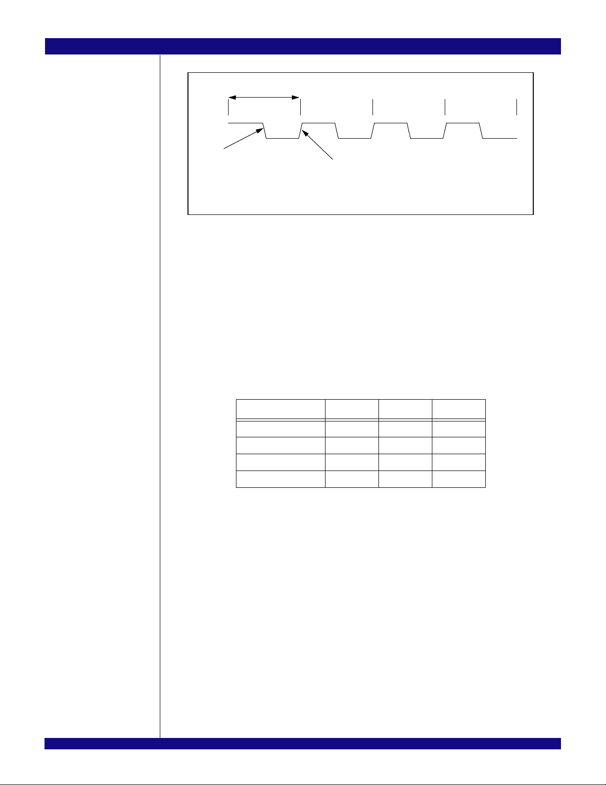
Throughout this manual, when describing signal transitions, the following terminology is used. Rising
edge indicates a low-to-high (0 to 1) transition. Falling edge indicates a high-to-low (1 to 0) transition. These
terms are illustrated in Figure 1.
PES32NT24xG2 User Manual 2 January 30, 2013
Page 5
IDT
Notes
1 2 3 4
high-to-low
transition
low-to-high
transition
single clock cycle
Figure 1 Signal Transitions
Numeric Representations
To represent numerical values, either decimal, binary, or hexadecimal formats will be used. The binary
format is as follows: 0bDDD, where “D” represents either 0 or 1; the hexadecimal format is as follows:
0xDD, where “D” represents the hexadecimal digit(s); otherwise, it is decimal.
The compressed notation ABC[x|y|z]D refers to ABCxD, ABCyD, and ABCzD.
The compressed notation ABC[y:x]D refers to ABCxD, ABC(x+1)D, ABC(x+2)D,... ABCyD.
Data Units
The following data unit terminology is used in this document.
Term Words Bytes Bits
Byte 1/2 1 8
Word 1 2 16
Doubleword (DWord) 2 4 32
Quadword (QWord) 4 8 64
Table 1 Data Unit Terminology
In quadwords, bit 63 is always the most significant bit and bit 0 is the least significant bit. In doublewords, bit 31 is always the most significant bit and bit 0 is the least significant bit. In words, bit 15 is always
the most significant bit and bit 0 is the leas t significant bit. In bytes, bit 7 is always the most significant bit
and bit 0 is the least significant bit.
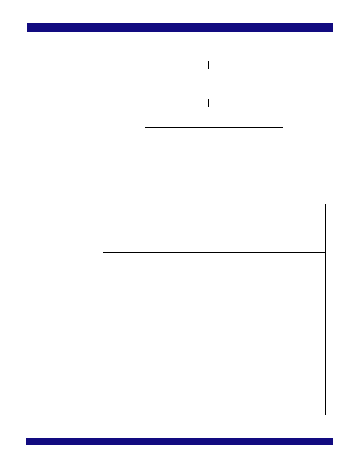
The ordering of bytes within words is referred to as either “big endian” or “little endian.” Big endian
systems label byte zero as the most significant (leftmost) byte of a word. Little endian systems label byte
zero as the least significant (rightmost) byte of a word. See Figure 2.
PES32NT24xG2 User Manual 3 January 30, 2013
Page 6
IDT
Notes
0 1 2 3
bit 0bit 31
Address of Bytes within Words: Big Endian
3 2 1 0
bit 0bit 31
Address of Bytes within Words: Little Endian
Figure 2 Example of Byte Ordering for “Big Endian” or “Little Endian” System Definition
Register Terminology
Software in the context of this register terminology refers to modifications made by PCI Express root
configuration writes, writes to registers made through the slave SMBus interface, or serial EEPROM
register initialization. See Table 2.
Type Abbreviation Description
Hardware Initialized HWINIT Register bits are initialized by firmware or hardware mechanisms
such as pin strapping or serial EEPROM. (System firmware hardware initialization is only allowed for system integrated devices.)
Bits are read-only after initialization and can only be reset (for
write-once by firmware) with reset.
Read Only and Clear RC Software can read the register/bits with this attribute. Reading the
value will automatically cause the register/bit to be reset to zero.
Writing to a RC location has no effect.
Read Clear and Write RCW Software can read the register/bits with this attribute. Reading the
value will automatically cause the register/bits to be reset to zero.
Writes cause the register/bits to be modified.
Reserved Reserved The value read from a reserved register/bit is undefined. Thus,
software must deal correctly with fields that are reserved. On
reads, software must use appropriate masks to extract the defined
bits and not rely on reserved bits being any particular value. On
writes, software must ensure that the values of reserved bit positions are preserved. That is, the values of reserved bit positions
must first be read, merged with the new values for other bit positions and then written back.
In addition to reserved registers, some valid register fields have
encodings marked as reserved. Such register fields must never be
written with a value corresponding to an encoding marked as
reserved. Violating this rule produces undefined operation in the
device.
Read Only RO Software can only read registers/bits with this attribute. Contents
Table 2 Register Terminology (Part 1 of 2)
PES32NT24xG2 User Manual 4 January 30, 2013
are hardwired to a constant value or are status bits that may be
set and cleared by hardware. Writing to a RO location has no
effect.
Page 7

IDT
Notes
Type Abbreviation Description
Read and Write RW Software can both read and write bits with this attribute.
Read and Write Clear RW1C Software can read and write to registers/bits with this attribute.
However, writing a value of zero to a bit with this attribute has no
effect. A RW1C bit can only be set to a value of 1 by a hardware
event. To clear a RW1C bit (i.e., change its value to zero) a value
of one must be written to the location. An RW1C bit is never
cleared by hardware.
Read and Write when
Unlocked
Sticky Sticky Register/bits with this designation take on their initial value as a
Switch Sticky SWSticky Register/bits with this designation take on their default value as a
Modified Switch Sticky MSWSticky A MSWSticky register is a Switch Sticky register that in addition to
Table 2 Register Terminology (Part 2 of 2)
Software can read the register/bits with this attribute. Writing to
register/bits with this attribute will only cause the value to be modified if the REGUNLOCK bit in the SWCTL register is set. When
the REGUNLOCK bit is cleared, writes are ignored and the register/bits are effectively read-only.
result of a switch fundamental reset or partition fundamental reset.
Other resets have no effect.
result of a switch fundamental reset. Other resets have no effect.
taking on its default value as a result of a switch fundamental
reset, it takes on its default value when the event(s) defined in the
register description occur, unless the register has been written-to
by software/firmware before the occurrence of the event.
If the value of an MSWSticky register has been written by software/firmware, it preserves the value across all events until written
again or until a switch fundamental reset is applied to the device.
After a switch fundamental reset, the MSWSticky register will
return to taking on the value as defined in the register description.
Use of Hypertext
In Chapter 19, Tables 19.2, 19.5, 19.6, 19.10, and 19.11 contain register names and page numbers
highlighted in blue under the Register Definition column. In pdf fil es, users can jump from thi s source table
directly to the registers by clicking on the register name in the source table. Each register name in the table
is linked directly to the appropriate register in Chapters 20 through 24. To return to the source table after
having jumped to the register section, click on the same register name (in blue) in the register section.
Reference Documents
PCI Express Base Specification Revision 2.1., March 4, 2009, PCI-SIG.
PCI Local Bus Specification Revision 3.0., February 3, 2004, PCI-SIG.
PCI-to-PCI Bridge Architecture Specification Revision 1.2., June 9, 2003, PCI-SIG.
Address Translation Services Specification, March 8, 2007, PCI-SIG.
PCI Bus Power Management Interface Specification, Revision 1.2., March 3, 2004, PCI-SIG
SMBus Specification, Version 2.0, August 3, 2000, SBS Implementers Forum.
Revision History
July 8, 2009: Initial publication of preliminary user manual.
PES32NT24xG2 User Manual 5 January 30, 2013
Page 8

IDT
Notes
July 14, 2009: Includes changes in several chapters based on recent updates in the functional specification.
July 30, 2009: Includes changes in several chapters based on recent updates in the functional specification.
August 28, 2009: Added Chapter 27, Usage Models.
September 18, 2009: In Chapter 2, added Table 2.5. In Chapter 4, added new sections Packet Routing
Classes and Proprietary Weighted Round Robin (WRR) Arbitration, and revised Figure 4.8. Made
numerous revisions in Chapter 8. In Chapter 10, made changes to the Action Taken column in Table 10.14.
In Chapter 12, updated the I/O Expander tables. In Chapter 15, made changes to Table 15.7 and added text
to DMA Multicast section. In Chapter 25, made numerous changes in SerDes x Transmitter Lane Control 0
and 1 registers
October 6, 2009: In Chapter 3, added text to section Switch Fundamental Rest and moved this section
in front of Boot Configuration Vector section, and added text to Switch Modes section. In Chapter 5, added
text to sections Switch Partitioning and Non-Transparent Operations. In Chapter 15, modified sections Data
Transfer and Addressing, Source Address E xpired Error, and Destination Address Expired Er ror. In Chapter
16, added text to section Switch Signals. In Chapter 21, modified description for bit EIS in the PCIESSTS
register. In Chapter 24, modified description of RUN bit in the DMAC[1:0]CTL register.
October 14, 2009: In Chapter 22, added WRR Port Arbitration Counts registers, and in Chapter 20,
updated Figure 20.2 and Table 20.5 to show new registers. Corrected Table 26.2, Boundary Scan Chain.
November 4, 2009: In Chapter 2, added new section Support for Spread Spectrum Clocking (SCC) with
updated tables and modified Limitations column in Table 2.6, Clock Frequency Limitations. In Chapter 5,
added three new sections: Partition State Change Latency, Port Operating Mode Change Latency, and
Partition Reconfiguration Latency. In Chapter 8, deleted all references to Slew Rate. In Chapter 10, title for
Table 10.11 was changed to Unexpected Completions instead of Unsupported Requests, and a new bullet
was added at the top of section Address Routed TLPs. In Chapter 14, modified text in Overview section and
in section Unsupported Request (UR) Error. In Chapter 15, modified text in section Reception of a Request
TLP That is Unsupported. In Chapter 19, added reference to junction temperature in the Overview section.
In Chapter 20, added new section Configuration Register Side-Effects under Overview. In Chapter 24, DMA
Channel Error Mask register, de-featured bits 2 and 17. In Chapter 25, SMBus Control register, de-featured
bit 16 (MSMBIOM).
November 23, 2009: In Chapter 4, corrected port numbers for Stack 1 in Figure 4.1.
December 4, 2009: In Chapter 10, modified text in section Error Emulation Control in the PCI-to-PCI
Bridge Function and added new section Error Emulation Usage and Limitations. In Chapter 14, modified
text in section Error Emulation Control in the NT Function and added new section Error Emulation Usage
and Limitations.
January 6, 2010: In Chapter 17, corrected references to NT Multicast Control register and NT Multicast
Transmit Enable bit in the following sections: NT Multicast TLP Routing, and Usage Restrictions. In Chapter
20, corrected Figure 20.5. In Chapter 23, NTIERRORMSK0 register, changed bits 29 and 30 to reserved. In
Chapter 24, DMAIERRORMSK0 register, changed bits 29 and 30 to reserved. In Chapter 25, changed
default values for several bits in the TMPADJA and TSSLOPE registers.
March 4, 2010: Revised manual to include references to the PES32NT24BG2 device in Chapters 1, 2,
3, 12, and 26 as appropriate and changed manual name to PES32NT24xG2.
March 8, 2010: Removed references to OUTDBELLCLR and OUTSBELLDBELLCLR registers in
Chapter 14, Non-Transparent Switch Operation.
March 17, 2010: In Chapter 8, updated Tables 8.6, 8.7, 8.8, 8.11, and 8.12. In Chapter 13, deleted re ference to multiple GPIOAFSEL registers; there is only one register. In Chapter 24, deleted “other” from ECRC
Error name for bit 31 in the DMAC[1:0]ERRSTS register.
May 10, 2010: In Chapter 21, PCI Bridge Registers, the ACSCAP register offset address was corrected
to 0x324. In Chapter 23, NT Endpoint Register, revised the Description for MODE field in BARSETUP0
register and LADDR field in BARLIMIT0 register.
PES32NT24xG2 User Manual 6 January 30, 2013
Page 9

IDT
Notes
May 21, 2010: In Chapter 23, NT Endpoint Registers, revised Description for INDEX field in
LUTOFFSET register to read that if BAR4 is selected, the INDEX field must only be set to values 0 to 11
(instead of 12 to 23).
June 21, 2010: In Chapter 23, NT Endpoint Registers, revised Bit Field column in NTMTBLDATA
register.
August 27, 2010: In Chapter 4, revised text in sections Internal Errors and Reporting of Port AER Errors
as Internal Errors and updated Figures 4.7 and 4.8. In Chapter 5, revised text in Reset Mode Change
Behavior. In Chapter 7, revised text in Link Width Negotiation in the Presence of Bad Lanes section and
Crosslink section. In Chapter 11, corrected reference to DLLLASC in Hot Plug Events section. In Chapter
12, revised description for BYTECNT in Tables 12.19 and 12.21. In Chapter 14, added Note at end of
section NT Mapping Table. In Chapter 15, deleted section DMA Channel Errors and revised text in
Descriptor Prefetching, ECRC Errors, and Completion Timeout sections. In Chapter 16, revised text in
section Port AER Errors. In Chapter 17, changed reference from NTMTC to NTMCC in NT Multicast TLP
Routing section.
In Chapter 21, made the following changes: revised description for MAXLNKSPD bit in PCI Express Link
Capabilities register (also applies to same bit in same register in Chapters 23 and 24), revised description
for bits in PCI Express Slot Control register.
In Chapter 22, made the following changes: added text under section Physical Layer Control and Status
Registers, revised description for bits in PCI Express Slot C ontrol Initial Value register, deleted Port AER
Status register, revised Port AER Mask register, added bit 10 to bit 9 as Reserved and revised description
for ILSCC bit in Phy Link Configuration 0 register.
In Chapter 23, made the following changes: revised PCI Express Device Capabilities 2 and PCI Express
Device Control 2 registers, revised Description for REG and EREG bits in ECFGADDR register, added bits
31:16 row in AER Correctable Error Status register, added text in Description of NXTPTR in SNUMCAP
register, added text in Description of NXTPTR in PCIEVCECAP register, revised information for fields
PARBC and PATBLOFF in VCR0CAP register, revised information for fields LPAT and PARBSEL in
VCR0CTL register, revised Description for PATS in VCR0STS register, added text in Description of
NXTPTR in ACSECAPH register, added text in Description of NXTPTR in MCCAPH register, changed
default value for bits 30:29 from 0x1 to 0x3 in NTIERRORMSK0 register, changed bit 6 in the NTINTMSK
register to Reserved, revised description for bits SIZE and MODE in Bar 0 Setup register, revised information in LADDR field in BARLIMIT0 register, revised text under register title for BAR 1 Limit Address and
changed Default Value for Reserved and LADDR and Description for LADDR, revised text under register
title for BARLIMIT3 and changed Default Value for Reserved and LADDR and Description for LADDR,
revised Default Value and Description for LADDR field in BARLIMIT4 register, revised text under register
title for BARLIMIT5 and changed Default Value and Description for LADDR, revised description for INDEX
in LUTOFFSET register.
In Chapter 24, made the following changes: revised bits 4 to 21 in PCIEDCAP2 register , r evised bit s 4 to
15 in PCIEDCTL2 register, revised bits 21 and 22 and added bits 24 and 25 in AERUES register, revised bit
22 and added bits 24 and 25 in AERUEM register, revised bit 22 and added bits 24 and 25 in AERUESV
register, changed Default Value for CIE bit in AERCES register, changed Type and Default Value for
ECRCGC and ECRCCC bits in AERCTL register, changed bit 24 (HEC) to reserved in DMAIERRORMSK1
register, de-featured bits 0 and 6 through 9 in the DMAC[1:0]ERRSTS register, de-featured bits 0 and 6
through 7 and changed name of bit 31 to ECRCE in DMAC[1:0]ERRMSK register.
In Chapter 25, made the following changes: revised SESTS register, revised description for COUNT
field in FCAP[3:0]TIMER register, added bits 20 and 21 and revised default value and/or description for bits
22 to 25 and changed name/value/description of bit 29 in SMBUSSTS register, removed default value for
TEMP field in TMPSTS register.
September 27, 2010: In Chapter 22, changed bit 16 in the IERRORSTS0 register from ULD to
Reserved.
October 22, 2010: In Chapter 15, added footnote to T able 15.7. In Chapter 25, re-arranged bits 24:28 in
TMPCTL register.
PES32NT24xG2 User Manual 7 January 30, 2013
Page 10

IDT
Notes
December 21, 2010: In Chapter 2, revised header in Table 2.6 to read “Initial Port Clock Mode.” In
Chapter 5, added new footnote #1 in section Port Operating Mode Change. In Chapter 15, deleted reference to DATCT bit in Completion Timeout section. In Chapter 23, added text to SUBVID and SUBID registers. In Chapter 24, changed bit 20 (DATCT bit) in the DMAC[1:0]ERRSTS and DMAC[1:0]ERRMSK
registers to Reserved and added text to SUBVID and SUBID registers. In Chapter 26, deleted PERSTN,
GLK1, and SMODE from Table 26.1.
March 11, 2011: In Chapter 26, revised Usage Considerations section to remove reference to
JTAG_TCK being driven to a known value.
March 25, 2011: In Chapter 22, added PHYLSTATE0 register with FLRET bit description.
May 20, 2011: In Chapter 1, added ZC silicon to Table 1.2.
June 21, 2011: In Chapter 5, section Reset Mode Change Behavior, changed fourth bullet to read “The
port remains in a Reset state for at least 250 µs.”
June 24, 2011: In Chapter 25, added bit BDISCARD to the Switch Control register.
July 15, 2011: In Chapter 1, revised section Switch Events and removed “and Signals” from the section
title. In Chapter 5, revised the following sections: Downstream Switch Port, Port Operating Mode Change
Latency, and System Notification of Partition Reconfiguration. In Chapter 8, revised section Programmable
De-emphasis Adjustment. In Chapter 16, removed “and Signals” from title and revised section Global
Signals and deleted Signals section. In Chapter 21, MCBLKALLH register, changed lower 32 to upper 32 in
description of MCBLKALL bit. In Chapters 22 and 23, deleted references to SSIGNAL field. In Chapter 25,
added section Internal Switch Timers with 4 new registers and deleted SSIGNAL register. Updated Figure
20.5 and Table 20.11, Switch Configuration and Status, in Chapter 20 to account for new registers.
July 27, 2011: In Chapter 22, added bits 7:0 (
RCVD_OVRD) in SERDESCFG register.
August 23, 2011: In Chapter 24, DMACxCFG register, changed 0x2 in DPREFETCH field to Reserved.
September 12, 2011: In Chapter 8, added additional reference in last paragraph of section Driver
Voltage Level and Amplitude Boost.
October 24, 2011: In Chapter 22, added Port Control Register. In Chapter 20, added reference to Port
Control register in Table 20.5.
November 7, 2011: In Chapter 2, section Local Port Clocked Mode, added recommendation to tie
unused port clock pins to ground.
December 4, 2011: In Chapter 25, revised Description for AFSEL0 field in the GPIOAFSEL register.
January 11, 2012: Removed Hardware Error Containment chapter. Deleted references to SWFRST bit.
February 8, 2012: In Chapter 12, added footnote for RERR and WERR bits in Table 12.20.
February 23, 2012: Added paragraph after Table 12.19 to explain use of DWord addresses.
March 14, 2012: In the Overview section of Chapter 2, changed “single” to ”two” differential global refer-
ence clock pairs.
May 1, 2012: In Chapter 2, Clocking, made text changes to state that unused port clock pins should be
connected to Vss on the board. In Chapter 12, SMBus Interfaces, added new section Setting Up I2C
Commands for Block Transactions.
June 27, 2012: In Chapter 12, changed BYTCNT=7 to BYTCNT=4 in Figure 12.14. In Chapter 24,
changed type and default values for bits 16 and 20 in Switch Control register.
January 30, 2013: In Figure 12.12, changed No-ack to Ack between DATALM and DATAUM.
PES32NT24xG2 User Manual 8 January 30, 2013
Page 11

Notes
Table of Contents
®
About This Manual
Overview ........................................................................................................................................1
Content Summary ..........................................................................................................................1
Signal Nomenclature .....................................................................................................................2
Numeric Representations ..............................................................................................................3
Data Units ......................................................................................................................................3
Register Terminology .....................................................................................................................4
Use of Hypertext ............................................................................................................................5
Reference Documents ...................................................................................................................5
Revision History .............................................................................................................................5
PES32NT24xG2 Device Overview
Overview.........................................................................................................................................1-1
System Identification.......................................................................................................................1-1
Vendor ID................................................................................................................................1-1
Device ID................................................................................................................................1-1
Revision ID.............................................................................................................................1-1
JTAG ID..................................................................................................................................1-2
SSID/SSVID............................................................................................................................1-2
Device Serial Number Enhanced Capability...........................................................................1-2
Architectural Overview....................................................................................................................1-2
Port Operating Modes.....................................................................................................................1-3
Switch Partitioning..........................................................................................................................1-6
Non-Transparent Operation............................................................................................................1-8
DMA Operation.............................................................................................................................1-12
Dynamic Reconfiguration and Failover.........................................................................................1-15
Switch Events...............................................................................................................................1-16
Multicasting and Non-Transparent Multicasting............................................................................1-17
Clocking
Overview.........................................................................................................................................2-1
Port Clocking Modes.......................................................................................................................2-2
Global Clocked Mode.............................................................................................................2-3
Local Port Clocked Mode........................................................................................................2-4
Support for Spread Spectrum Clocking (SSC).......................................................................2-5
Port Clocking Mode Selection.................................................................................................2-6
System Clocking Configurations.....................................................................................................2-8
Reset and Initialization
Overview.........................................................................................................................................3-1
Switch Fundamental Reset.............................................................................................................3-2
Boot Configuration Vector...............................................................................................................3-4
Stack Configuration.........................................................................................................................3-5
Static Configuration of a Stack...............................................................................................3-9
Dynamic Reconfiguration of a Stack via EEPROM / SMBus..................................................3-9
Switch Modes.......................................................................................................................3-10
Partition Resets.............................................................................................................................3-11
PES32NT24xG2 User Manual i January 30, 2013
Page 12

IDT Table of Contents
Notes
Partition Fundamental Reset................................................................................................3-12
Partition Hot Reset ...............................................................................................................3-12
Partition Upstream Secondary Bus Reset............................................................................3-13
Partition Downstream Secondary Bus Reset .......................................................................3-14
Port Mode Change Reset.............................................................................................................3-14
Switch Core
Overview.........................................................................................................................................4-1
Switch Core Architecture................................................................................................................4-1
Ingress Buffer.........................................................................................................................4-2
Egress Buffer..........................................................................................................................4-3
Crossbar Interconnect............................................................................................................4-4
Virtual Channel Support..................................................................................................................4-5
Packet Routing Classes..................................................................................................................4-5
Packet Ordering..............................................................................................................................4-6
Arbitration .......................................................................................................................................4-6
Port Arbitration........................................................................................................................4-6
Cut-Through Routing......................................................................................................................4-9
Request Metering .........................................................................................................................4-11
Operation..............................................................................................................................4-13
Completion Size Estimation..................................................................................................4-14
Internal Errors...............................................................................................................................4-16
Switch Core Time-Outs ........................................................................................................4-17
Memory SECDED ECC Protection.......................................................................................4-18
End-to-End Data Path Parity Protection...............................................................................4-18
Reporting of Port AER Errors as Internal Errors...................................................................4-19
Switch Partition and Port Configuration
Overview.........................................................................................................................................5-1
Switch Partitions.............................................................................................................................5-1
Partition Configuration............................................................................................................5-2
Partition State.........................................................................................................................5-3
Partition State Change ...........................................................................................................5-4
Switch Ports....................................................................................................................................5-5
Switch Port Mode ...................................................................................................................5-5
Port Operating Mode Change.......................................................................................................5-13
Common Operating Mode Change Behavior .......................................................................5-15
No Action Mode Change Behavior.......................................................................................5-21
Reset Mode Change Behavior .............................................................................................5-21
Partition Reconfiguration and Failover..........................................................................................5-21
Partition Reconfiguration Latency.........................................................................................5-23
System Notification of Partition Reconfiguration ..................................................................5-23
Failover
Overview.........................................................................................................................................6-1
Failover Initiation.............................................................................................................................6-1
Software Initiated Failover......................................................................................................6-2
Signal Initiated Failover..........................................................................................................6-2
Watchdog Timer Initiated Failover..........................................................................................6-2
PES32NT24xG2 User Manual ii January 30, 2013
Page 13

IDT Table of Contents
Notes
Link Operation
Overview.........................................................................................................................................7-1
Port Merging...................................................................................................................................7-1
Port Maximum Link Width...............................................................................................................7-1
Polarity Inversion............................................................................................................................7-2
Lane Reversal.................................................................................................................................7-2
Link Width Negotiation....................................................................................................................7-4
Link Width Negotiation in the Presence of Bad Lanes ...........................................................7-5
Dynamic Link Width Reconfiguration..............................................................................................7-5
Dynamic Link Width Reconfiguration in the PES32NT24xG2................................................7-6
Link Speed Negotiation...................................................................................................................7-6
Link Speed Negotiation in the PES32NT24xG2.....................................................................7-7
Software Management of Link Speed ....................................................................................7-8
Link Retraining................................................................................................................................7-9
Link States......................................................................................................................................7-9
Link Down Handling......................................................................................................................7-10
Slot Power Limit Support..............................................................................................................7-11
Upstream Port ......................................................................................................................7-11
Downstream Switch Port......................................................................................................7-12
Link Active State Power Management (ASPM)............................................................................7-12
L0s ASPM.............................................................................................................................7-12
L1 ASPM ..............................................................................................................................7-13
Link Status....................................................................................................................................7-16
De-emphasis Negotiation .............................................................................................................7-16
Crosslink.......................................................................................................................................7-17
Hot Reset Operation on a Crosslink.....................................................................................7-17
Link Disable Operation on a Crosslink .................................................................................7-18
Gen 1 Compatibility Mode ............................................................................................................7-18
SerDes
Overview.........................................................................................................................................8-1
SerDes Numbering and Port Association.......................................................................................8-1
SerDes Transmitter Controls..........................................................................................................8-3
Driver Voltage Level and Amplitude Boost.............................................................................8-3
De-emphasis ..........................................................................................................................8-4
PCI Express Low-Swing Mode...............................................................................................8-4
Receiver Equalization.....................................................................................................................8-4
Programming of SerDes Controls...................................................................................................8-4
Programmable Voltage Margining and De-Emphasis ............................................................8-5
SerDes Transmitter Control Registers....................................................................................8-6
Transmit Margining Using the PCI Express Link Control 2 Register....................................8-12
Low-Swing Transmitter Voltage Mode..........................................................................................8-12
Receiver Equalization Controls.....................................................................................................8-14
SerDes Power Management.........................................................................................................8-14
Power Management
Overview.........................................................................................................................................9-1
Power Management Event (PME) Messages.................................................................................9-4
PCI Express Power Management Fence Protocol .........................................................................9-4
Upstream Switch Port or Downstream Switch Port Mode......................................................9-4
NT Function Mode or NT with DMA Function Mode...............................................................9-5
Upstream Switch Port with NT and/or DMA Function Mode...................................................9-5
PES32NT24xG2 User Manual iii January 30, 2013
Page 14

IDT Table of Contents
Notes
Transparent Switch Operation
Overview.......................................................................................................................................10-1
Transaction Routing......................................................................................................................10-1
Virtual Channel Support................................................................................................................10-2
Maximum Payload Size................................................................................................................10-2
Upstream Port Device Number.....................................................................................................10-2
Bus Locking..................................................................................................................................10-2
Interrupts.......................................................................................................................................10-4
Downstream Port Interrupts..................................................................................................10-4
Upstream Port Interrupts......................................................................................................10-4
Legacy Interrupt Aggregation...............................................................................................10-5
Access Control Services...............................................................................................................10-6
ECRC Support............................................................................................................................10-10
Error Detection and Handling by the PCI-to-PCI Bridge Function..............................................10-11
Physical Layer Errors .........................................................................................................10-11
Data Link Layer Errors........................................................................................................10-12
Transaction Layer Errors....................................................................................................10-13
Routing Errors ....................................................................................................................10-23
Error Emulation Control in the PCI-to-PCI Bridge Function................................................10-24
Hot-Plug and Hot-Swap
Overview.......................................................................................................................................11-1
Hot-Plug Signals...........................................................................................................................11-3
Port Reset Outputs.......................................................................................................................11-5
Power Enable Controlled Reset Output................................................................................11-5
Power Good Controlled Reset Output..................................................................................11-6
Hot-Plug Events............................................................................................................................11-7
Legacy System Hot-Plug Support.................................................................................................11-7
Hot-Swap......................................................................................................................................11-8
SMBus Interfaces
Overview.......................................................................................................................................12-1
Master SMBus Interface...............................................................................................................12-1
Initialization and I
Serial EEPROM...................................................................................................................12-2
Initialization from Serial EEPROM........................................................................................12-3
Programming the Serial EEPROM.....................................................................................12-10
I/O Expanders.....................................................................................................................12-11
Slave SMBus Interface...............................................................................................................12-22
Initialization.........................................................................................................................12-22
SMBus Transactions ..........................................................................................................12-23
Setting Up I2C Commands for Block Transactions.....................................................................12-29
CSR Register Read or Write Operation..............................................................................12-29
SMBus Transactions ..........................................................................................................12-30
Examples of Setting Up the I2C CSR Byte Sequence for a CSR Register Read...............12-32
Examples of Setting Up the I2C CSR Byte Sequence for a CSR Register Write...............12-35
2
C Reset...................................................................................................12-1
General Purpose I/O
Overview.......................................................................................................................................13-1
GPIO Configuration ......................................................................................................................13-1
Input......................................................................................................................................13-1
Output...................................................................................................................................13-1
Alternate Function ................................................................................................................13-1
PES32NT24xG2 User Manual iv January 30, 2013
Page 15

IDT Table of Contents
Notes
Non-Transparent Switch Operation
Overview.......................................................................................................................................14-1
Base Address Registers (BARs)...................................................................................................14-1
BAR Limit..............................................................................................................................14-2
Mapping NT Configuration Space to BAR 0.........................................................................14-4
TLP Translation ............................................................................................................................14-4
Direct Address Translation...................................................................................................14-4
Lookup Table Address Translation.......................................................................................14-5
ID Translation ...............................................................................................................................14-9
NT Mapping Table................................................................................................................14-9
Request ID Translation.......................................................................................................14-11
Completion ID Translation..................................................................................................14-13
Requester ID Capture Register..........................................................................................14-14
TLP Attribute Processing............................................................................................................14-14
No Snoop Processing.........................................................................................................14-14
Address Type Processing...................................................................................................14-15
NT Multicast................................................................................................................................14-15
Inter-Domain Communications...................................................................................................14-15
Doorbell Registers..............................................................................................................14-16
Message Registers.............................................................................................................14-17
Punch-Through Configuration Requests ....................................................................................14-18
Re-programming the Bus Number of the NT Function...............................................................14-19
Interrupts.....................................................................................................................................14-20
Virtual Channel Support..............................................................................................................14-21
Maximum Payload Size..............................................................................................................14-22
Power Management...................................................................................................................14-22
Bus Locking................................................................................................................................14-22
ECRC Support............................................................................................................................14-22
Access Control Services (ACS)..................................................................................................14-23
Error Detection and Handling by the NT Function......................................................................14-25
Physical Layer Errors .........................................................................................................14-26
Data Link Layer Errors........................................................................................................14-26
Transaction Layer Errors....................................................................................................14-26
NTB Inter-Partition Error Propagation ................................................................................14-31
Error Emulation Control in the NT Function........................................................................14-39
Non Transparent Operation Restrictions....................................................................................14-40
DMA Controller
Overview.......................................................................................................................................15-1
Base Address Registers...............................................................................................................15-1
DMA Channel Functional Description...........................................................................................15-1
Data Transfer and Addressing..............................................................................................15-2
DMA Descriptors ..................................................................................................................15-6
DMA Descriptor Processing ...............................................................................................15-15
TLP Attribute and Traffic Class Control..............................................................................15-20
Channel Interrupts..............................................................................................................15-21
DMA Outstanding Requests...............................................................................................15-21
Descriptor Prefetching........................................................................................................15-22
DMA Request Rate Control................................................................................................15-22
PES32NT24xG2 User Manual v January 30, 2013
Page 16

IDT Table of Contents
Notes
DMA Multicast ....................................................................................................................15-23
Interrupts.....................................................................................................................................15-24
Virtual Channel (VC) Support.....................................................................................................15-25
Access Control Services (ACS) Support ....................................................................................15-25
Power Management....................................................................................................................15-27
Bus Locking................................................................................................................................15-27
ECRC Support............................................................................................................................15-27
Error Handling.............................................................................................................................15-27
PCI Express Error Handling by the DMA Function.............................................................15-28
DMA Limitations and Usage Restrictions ...................................................................................15-36
Switch Events
Overview.......................................................................................................................................16-1
Switch Events...............................................................................................................................16-1
Link Up .................................................................................................................................16-2
Link Down.............................................................................................................................16-3
Fundamental Reset..............................................................................................................16-3
Hot Reset..............................................................................................................................16-3
Failover.................................................................................................................................16-3
Global Signals ......................................................................................................................16-4
Port AER Errors....................................................................................................................16-5
Multicast
Overview.......................................................................................................................................17-1
Transparent Multicast Operation ..................................................................................................17-1
Addressing and Routing.......................................................................................................17-1
Usage Restrictions ...............................................................................................................17-6
Non-Transparent Multicast Operation...........................................................................................17-6
NT Multicast Configuration...................................................................................................17-7
NT Multicast TLP Determination...........................................................................................17-8
NT Multicast TLP Routing.....................................................................................................17-8
NT Multicast Egress Processing...........................................................................................17-9
Usage Restrictions .............................................................................................................17-11
Temperature Sensor
Overview.......................................................................................................................................18-1
Register Organization
Overview.......................................................................................................................................19-1
Partial-Byte Access to Word and DWord Registers .............................................................19-3
Configuration Register Side-Effects .....................................................................................19-3
Address Maps...............................................................................................................................19-4
PCI-to-PCI Bridge Function Registers..................................................................................19-4
Proprietary Port-Specific Registers in the PCI-to-PCI Bridge Function..............................19-11
NT Function Registers........................................................................................................19-14
DMA Function Registers.....................................................................................................19-23
Switch Configuration and Status Registers........................................................................19-29
PES32NT24xG2 User Manual vi January 30, 2013
Page 17

IDT Table of Contents
Notes
PCI-to-PCI Bridge Registers
Type 1 Configuration Header Registers .......................................................................................20-1
PCI Express Capability Structure ...............................................................................................20-13
PCI Power Management Capability Structure............................................................................20-36
Message Signaled Interrupt Capability Structure .......................................................................20-38
Subsystem ID and Subsystem Vendor ID ..................................................................................20-39
Extended Configuration Space Access Registers......................................................................20-40
Advanced Error Reporting (AER) Extended Capability...............................................................20-41
Device Serial Number Extended Capability................................................................................20-51
PCI Express Virtual Channel Capability .....................................................................................20-52
ACS Extended Capability ...........................................................................................................20-55
Multicast Extended Capability.....................................................................................................20-60
Proprietary Port Specific Registers
Port Control Register....................................................................................................................21-1
Upstream PCI-to-PCI Bridge Interrupt and Signaling...................................................................21-1
Port AER Mask Register...............................................................................................................21-3
Port Slot Control ...........................................................................................................................21-5
Internal Error Control and Status Registers..................................................................................21-7
Physical Layer Control and Status Registers .............................................................................21-28
Request Metering .......................................................................................................................21-32
WRR Port Arbitration Counts......................................................................................................21-33
Non-Transparent Multicast Overlay............................................................................................21-38
AER Error Emulation ..................................................................................................................21-40
Global Address Space Access Registers...................................................................................21-43
NT Endpoint Registers
Type 0 Configuration Header Registers .......................................................................................22-1
PCI Express Capability Structure ...............................................................................................22-13
PCI Power Management Capability Structure............................................................................22-28
Message Signaled Interrupt Capability Structure .......................................................................22-29
Subsystem ID and Subsystem Vendor ID ..................................................................................22-31
Extended Configuration Space Access Registers......................................................................22-31
Advanced Error Reporting (AER) Extended Capability...............................................................22-33
Device Serial Number Extended Capability................................................................................22-43
PCI Express Virtual Channel Capability .....................................................................................22-44
ACS Extended Capability ...........................................................................................................22-48
Multicast Extended Capability.....................................................................................................22-50
NT Registers...............................................................................................................................22-53
NT Control & Status............................................................................................................22-53
NT Interrupt and Signaling..................................................................................................22-54
Internal Error Reporting Masks...........................................................................................22-56
Doorbell Registers..............................................................................................................22-64
Message Registers.............................................................................................................22-65
BAR Configuration..............................................................................................................22-67
Mapping Table....................................................................................................................22-85
Lookup Table..............................................................................................................................22-88
AER Error Emulation ..................................................................................................................22-89
Punch-Through Configuration Registers ....................................................................................22-92
NT Multicast................................................................................................................................22-94
Global Address Space Access Registers...................................................................................22-95
PES32NT24xG2 User Manual vii January 30, 2013
Page 18

IDT Table of Contents
Notes
DMA Function Registers
Type 0 Configuration Header Registers .......................................................................................23-1
PCI Express Capability Structure .................................................................................................23-9
PCI Power Management Capability Structure............................................................................23-22
Message Signaled Interrupt Capability Structure .......................................................................23-24
Extended Configuration Space Access Registers......................................................................23-25
Advanced Error Reporting (AER) Extended Capability...............................................................23-26
ACS Extended Capability ...........................................................................................................23-37
DMA Registers............................................................................................................................23-39
BAR Configuration..............................................................................................................23-39
DMA AER Error Emulation.................................................................................................23-39
Internal Error Reporting Masks...........................................................................................23-42
DMA Multicast Control........................................................................................................23-49
DMA Channel Registers.....................................................................................................23-50
Global Address Space Access Registers...................................................................................23-59
Switch Configuration and Status Registers
Switch Control and Status Registers............................................................................................24-1
Internal Switch Timers..................................................................................................................24-5
Switch Partition and Port Registers..............................................................................................24-7
Failover Capability Registers......................................................................................................24-13
Protection....................................................................................................................................24-15
Switch Event Registers...............................................................................................................24-16
Global Doorbells and Message Registers ..................................................................................24-25
SerDes Control and Status Registers.........................................................................................24-26
General Purpose I/O Registers...................................................................................................24-33
Hot-Plug and SMBus Interface Registers...................................................................................24-35
Temperature Sensor Registers...................................................................................................24-45
JTAG Boundary Scan
Introduction...................................................................................................................................25-1
Test Access Point.........................................................................................................................25-1
Signal Definitions..........................................................................................................................25-1
Boundary Scan Chain...................................................................................................................25-3
Test Data Register (DR)...............................................................................................................25-6
Boundary Scan Registers.....................................................................................................25-7
Instruction Register (IR)................................................................................................................25-8
EXTEST................................................................................................................................25-9
SAMPLE/PRELOAD.............................................................................................................25-9
BYPASS...............................................................................................................................25-9
CLAMP...............................................................................................................................25-10
IDCODE..............................................................................................................................25-10
VALIDATE..........................................................................................................................25-10
EXTEST_TRAIN.................................................................................................................25-10
EXTEST_PULSE................................................................................................................25-11
RESERVED........................................................................................................................25-11
Usage Considerations........................................................................................................25-11
Usage Models
Introduction...................................................................................................................................26-1
Boot-time Stack Reconfiguration..................................................................................................26-1
Port Clocking Configuration..........................................................................................................26-2
Boot-time Switch Partitioning........................................................................................................26-3
PES32NT24xG2 User Manual viii January 30, 2013
Page 19

IDT Table of Contents
Notes
Switch Partitioning via serial EEPROM................................................................................26-4
Switch Partitioning via PCI Express Configuration Requests...............................................26-5
Dynamic Port and Partition Reconfiguration.................................................................................26-8
I/O Load Balancing: Downstream Port Migration .................................................................26-8
Non-Transparent Bridge (NTB) Usage Models...........................................................................26-11
PES32NT24xG2 as a Multiprocessor System Interconnect...............................................26-11
NT Crosslink & NT Punch-Through....................................................................................26-15
DMA Usage Models....................................................................................................................26-17
High-Performance Multiprocessor System.........................................................................26-17
Immediate Descriptor Usage..............................................................................................26-20
Failover.......................................................................................................................................26-20
Active / Passive Failover Configuration..............................................................................26-20
Active / Active Failover Configuration.................................................................................26-23
Failover with Two Crosslinked PES32NT24xG2 Switches.................................................26-27
NT Multicasting...........................................................................................................................26-30
PES32NT24xG2 User Manual ix January 30, 2013
Page 20

IDT Table of Contents
Notes
PES32NT24xG2 User Manual x January 30, 2013
Page 21

Notes
List of Tables
®
Table 1.1 PES32NT24xG2 Device IDs................................................................................................1-1
Table 1.2 PES32NT24xG2 Revision ID...............................................................................................1-2
Table 1.3 Operating Modes Supported by Each Port..........................................................................1-6
Table 2.1 Ports That Must Operate with the Same Port Clocking Mode.............................................2-3
Table 2.2 PxCLK Usage When a Port Operates in Local Port Clocked Mode ....................................2-4
Table 2.3 GCLK and PxCLK frequencies when PxCLK has SSC.......................................................2-6
Table 2.4 Port Clocking Mode Requirements......................................................................................2-6
Table 2.5 Initial Port Clocking Mode and Slot Clock Configuration State............................................2-7
Table 2.6 Clock Frequency Limitations when Modifying a Port’s Clock Mode ....................................2-7
Table 2.7 Valid PES32NT24xG2 System Clocking Configurations.....................................................2-8
Table 3.1 PES32NT24xG2 Reset Precedence....................................................................................3-1
Table 3.2 Boot Configuration Vector Signals.......................................................................................3-5
Table 3.3 Ports in Each Stack.............................................................................................................3-6
Table 3.4 Possible Configurations for Stack 0.....................................................................................3-6
Table 3.5 Possible Configurations for Stack 1.....................................................................................3-6
Table 3.6 Possible Configurations for Stack 2.....................................................................................3-7
Table 3.7 Possible Configurations for Stack 3.....................................................................................3-8
Table 3.8 Normal Switch Modes........................................................................................................3-10
Table 3.9 Switch Mode Dependent Register Initialization.................................................................3-11
Table 4.1 IFB Buffer Sizes...................................................................................................................4-3
Table 4.2 EFB Buffer Sizes.................................................................................................................4-4
Table 4.3 Replay Buffer Storage Limit.................................................................................................4-4
Table 4.4 Packet Ordering Rules in the PES32NT24xG2...................................................................4-6
Table 4.5 Conditions for Cut-Through Transfers...............................................................................4-10
Table 4.6 Request Metering Decrement Value..................................................................................4-14
Table 5.1 Port Functions for Each Port Operating Mode.....................................................................5-7
Table 5.2 Port Operating Mode Changes Supported by the Switch..................................................5-14
Table 7.1 Crosslink Port Groups........................................................................................................7-17
Table 7.2 Gen 1 Compatibility Mode: bits cleared in training sets .....................................................7-18
Table 8.1 SerDes / Port Association for Ports in Stack 0....................................................................8-2
Table 8.2 SerDes / Port Association for Ports in Stack 1....................................................................8-2
Table 8.3 SerDes / Port Association for Ports in Stack 2....................................................................8-2
Table 8.4 SerDes / Port Association for Ports in Stack 3....................................................................8-3
Table 8.5 SerDes Transmit Level Controls in the S[x]TXLCTL0 and S[x]TXLCTL1 Registers............8-6
Table 8.6 SerDes Transmit Driver Settings in Gen 1 Mode with -3.5 dB de-emphasis.......................8-7
Table 8.7 SerDes Transmit Driver Settings in Gen 2 Mode with -3.5 dB de-emphasis.......................8-8
Table 8.8 SerDes Transmit Driver Settings in Gen 2 Mode with -6.0 dB de-emphasis.......................8-9
Table 8.9 PCI Express Transmit Margining Levels Supported by the PES32NT24xG2....................8-12
Table 8.10 SerDes Transmit Drive Swing in Low Swing Mode at Gen 1 speed..................................8-13
Table 8.11 SerDes Transmit Drive Swing in Low Swing Mode at Gen 2 Speed.................................8-13
Table 9.1 PES32NT24xG2 Power Management State Transition Diagram........................................9-2
Table 10.1 Switch Routing Methods....................................................................................................10-1
Table 10.2 PCI-to-PCI Bridge Function Interrupts...............................................................................10-4
Table 10.3 Downstream to Upstream Port Interrupt Routing Based on Device Number.....................10-6
Table 10.4 Prioritization of ACS Checks for Request TLPs.................................................................10-9
Table 10.5 Prioritization of ACS Checks for Completion TLPs..........................................................10-10
Table 10.6 TLP Types Affected by ACS Checks ...............................................................................10-10
Table 10.7 Physical Layer Errors.......................................................................................................10-12
Table 10.8 Data Link Layer Errors.....................................................................................................10-12
PES32NT24xG2 User Manual xi January 30, 2013
Page 22

IDT List of Tables
Notes
Table 10.9 Transaction Layer Errors Associated with the PCI-to-PCI Bridge Function.....................10-14
Table 10.10 Conditions Handled as Unsupported Requests (UR) by the PCI-to-PCI Bridge
Function...........................................................................................................................10-15
Table 10.11 Conditions Handled as Unexpected Completions (UC) by the PCI-to-PCI Bridge
Function...........................................................................................................................10-16
Table 10.12 Ingress TLP Formation Checks associated with the PCI-to-PCI Bridge Function...........10-17
Table 10.13 Egress Malformed TLP Error Checks..............................................................................10-18
Table 10.14 ACS Violations for Ports Operating in Downstream Switch Port Mode...........................10-19
Table 10.15 Prioritization of Transaction Layer Errors........................................................................10-20
Table 11.1 Port Hot Plug Signals........................................................................................................11-3
Table 11.2 Negated Value of Unused Hot-Plug Output Signals..........................................................11-4
Table 12.1 Serial EEPROM SMBus Address......................................................................................12-2
Table 12.2 PES32NT24xG2 Compatible Serial EEPROMs................................................................12-3
Table 12.3 Serial EEPROM Initialization Errors................................................................................12-10
Table 12.4 I/O Expander Functionality Allocation..............................................................................12-11
Table 12.5 Pin Mapping for I/O Expanders 0 through 11..................................................................12-15
Table 12.6 I/O Expander 0 through 11 Port Mapping........................................................................12-16
Table 12.7 Pin Mapping I/O Expander 12.........................................................................................12-16
Table 12.8 Pin Mapping of I/O Expander 13.....................................................................................12-17
Table 12.9 Pin Mapping I/O Expander 14.........................................................................................12-17
Table 12.10 Pin Mapping I/O Expander 15 .........................................................................................12-18
Table 12.11 Pin Mapping I/O Expander 16 .........................................................................................12-18
Table 12.12 Pin Mapping of I/O Expander 17 .....................................................................................12-19
Table 12.13 Pin Mapping of I/O Expander 18 .....................................................................................12-20
Table 12.14 Pin Mapping of I/O Expander 19 .....................................................................................12-20
Table 12.15 Pin Mapping of I/O Expander 20 .....................................................................................12-21
Table 12.16 Pin Mapping of I/O Expander 21 .....................................................................................12-22
Table 12.17 Slave SMBus Address.....................................................................................................12-23
Table 12.18 Slave SMBus Command Code Fields.............................................................................12-23
Table 12.19 CSR Register Read or Write Operation Byte Sequence.................................................12-24
Table 12.20 CSR Register Read or Write CMD Field Description.......................................................12-25
Table 12.21 Serial EEPROM Read or Write Operation Byte Sequence .............................................12-26
Table 12.22 Serial EEPROM Read or Write CMD Field Description ...................................................12-27
Table 12.23 CSR Register Read or Write Operation Byte Sequence.................................................12-30
Table 12.24 Slave SMBus Command Code Fields.............................................................................12-31
Table 12.25 CSR Register Read or Write CMD Field Description.......................................................12-31
Table 12.26 Constants Used in Examples ..........................................................................................12-32
Table 12.27 I2C Command Byte Array Indices...................................................................................12-33
Table 12.28 I2C Command Byte Array Indices...................................................................................12-34
Table 12.29 I2C Command Byte Array Indices...................................................................................12-35
Table 12.30 I2C Command Byte Array Indices...................................................................................12-36
Table 12.31 I2C Command Byte Array Indices...................................................................................12-37
Table 12.32 I2C Command Byte Array Indice.....................................................................................12-38
Table 13.1 GPIO Pin Configuration.....................................................................................................13-1
Table 13.2 GPIO Alternate Function Pin Assignment.........................................................................13-2
Table 13.3 GPIO Alternate Function Pins...........................................................................................13-2
Table 14.1 NT Endpoint BARs............................................................................................................14-2
Table 14.2 12-Entry Lookup Table Parameters...................................................................................14-7
Table 14.3 24-Entry Lookup Table Parameters...................................................................................14-8
Table 14.4 NT Mapping Table Field Description.................................................................................14-9
Table 14.1 NT Endpoint Interrupts....................................................................................................14-21
Table 14.2 ACS Checks Performed by the NT Function in a Port Operating in Multi-function Mode14-24
Table 14.3 TLP Types Affected by ACS Checks...............................................................................14-24
Table 14.4 Transaction Layer Errors Associated with the NT Function............................................14-27
Table 14.5 Conditions Handled as Unsupported Requests (UR) by the NT Function.......................14-29
PES32NT24xG2 User Manual xii January 30, 2013
Page 23

IDT List of Tables
Notes
Table 14.6 Conditions Handled as Unexpected Completion (UC) by the NT Function.....................14-30
Table 14.7 Error Logging at Each Function for UR Example # 1......................................................14-34
Table 14.8 Error Logging at Each Function for UR Example # 2......................................................14-35
Table 14.9 Error Logging at Each Function for Poisoned TLP Example...........................................14-36
Table 14.10 Error Logging at Each Function for Poisoned TLP Example...........................................14-38
Table 15.1 DMA Channel Addressing Parameters..............................................................................15-4
Table 15.2 Linear Addressing DMA Example......................................................................................15-5
Table 15.3 Constant Addressing DMA Example.................................................................................15-6
Table 15.4 Stride Control DMA Descriptor Fields................................................................................15-8
Table 15.5 Data Transfer DMA Descriptor Fields..............................................................................15-10
Table 15.6 Immediate Data Transfer DMA Descriptor Fields............................................................15-13
Table 15.7 DMA Chaining Disabling..................................................................................................15-17
Table 15.8 DMA Channel Control (DMACxCTL) Register Action Summary.....................................15-19
Table 15.9 Downstream Switch Port Interrupts.................................................................................15-25
Table 15.10 ACS Checks Performed by the DMA Function................................................................15-26
Table 15.11 TLP Types Affected by ACS Checks...............................................................................15-26
Table 15.12 PCI Express Errors Detected by the DMA Function’s Transaction Layer........................15-30
Table 15.13 Prioritization of Transaction Layer Errors........................................................................15-35
Table 19.1 Global Address Space Layout...........................................................................................19-1
Table 19.2 PCI-to-PCI Bridge Function Configuration Space Registers.............................................19-6
Table 19.3 Default Linkage of Capability Structures for a PCI-to-PCI Bridge Function in the
Upstream Switch Port Mode............................................................................................19-10
Table 19.4 Default Linkage of Capability Structures for a PCI-to-PCI Bridge Function in a
Downstream or Unattached Port.....................................................................................19-10
Table 19.5 Proprietary Port Specific Registers..................................................................................19-13
Table 19.6 NT Function Registers.....................................................................................................19-17
Table 19.7 Default Linkage of Capability Structures for the NT Function When Operating as
Function 0 of the Port......................................................................................................19-22
Table 19.8 Default Linkage of Capability Structures for the NT Function When Operating as
Function 1 of the Port......................................................................................................19-23
Table 19.9 Default Linkage of Capability Structures for the DMA Function......................................19-24
Table 19.10 DMA Function Registers..................................................................................................19-26
Table 19.11 Switch Configuration and Status .....................................................................................19-31
Table 25.1 JTAG Pin Descriptions......................................................................................................25-2
Table 25.2 Boundary Scan Chain........................................................................................................25-3
Table 25.3 Instructions Supported by the JTAG Boundary Scan........................................................25-9
Table 25.4 System Controller Device Identification Register............................................................25-10
PES32NT24xG2 User Manual xiii January 30, 2013
Page 24

IDT List of Tables
Notes
PES32NT24xG2 User Manual xiv January 30, 2013
Page 25

Notes
List of Figures
®
Figure 1.1 PES32NT24xG2 Block Diagram ........................................................................................1-3
Figure 1.2 Logical Representation of a Port with PCI-to-PCI bridge, NT, and DMA Functions ..........1-5
Figure 1.3 Transparent PCI Express Switch .......................................................................................1-6
Figure 1.4 Partitionable PCI Express Switch ......................................................................................1-7
Figure 1.5 Non-Transparent Bridge ....................................................................................................1-8
Figure 1.6 Generalized Multi-Port Non-Transparent Interconnect ......................................................1-9
Figure 1.7 Architectural Approaches for Integrating Non-Transparency into a PCI Express Switch .1-10
Figure 1.8 Non-Transparent Switch with Non-Transparency Between Partitions .............................1-11
Figure 1.9 Non-Transparent Switch with Non-Transparent Ports .....................................................1-11
Figure 1.10 Non-Transparent Switch with Non-Transparent Ports .....................................................1-12
Figure 1.11 Non-Transparent Switch with Non-Transparent Ports .....................................................1-12
Figure 1.12 Switch Partition with DMA function ..................................................................................1-13
Figure 1.13 Two Switch Partitions Interconnected by an NTB, with DMA in One Partition .................1-14
Figure 1.14 Two Switch Partitions Interconnected by an NTB, with DMA in Both Partitions ..............1-15
Figure 1.15 Non-Transparent Switch Failover Usage .........................................................................1-16
Figure 1.16 Example of Switch Event Mechanism ..............................................................................1-17
Figure 1.17 Example of Transparent Multicast ...................................................................................1-18
Figure 1.18 Example of Non Transparent Multicast ............................................................................1-18
Figure 2.1 Logical Representation of PES32NT24AG2 Clocking Architecture ...................................2-2
Figure 2.2 Logical Representation of PES32NT24BG2 Clocking Architecture ...................................2-2
Figure 2.3 Clocking Connection for a Port in Global Clocked Mode, with a Common Clocked
Configuration ......................................................................................................................2-3
Figure 2.4 Clocking Connection for a Port in Global Clocked Mode, Non-Common Clocked
Configuration ......................................................................................................................2-4
Figure 2.5 Clocking Connection for a Port in Local Port Clocked Mode, in a Common Clocked
Configuration ......................................................................................................................2-5
Figure 2.6 Clocking Connection for a Port in Local Port Clocked Mode, in a Non-Common
Clocked Configuration ........................................................................................................2-5
Figure 3.1 Switch Fundamental Reset with Serial EEPROM Initialization ..........................................3-3
Figure 3.2 Fundamental Reset Using RSTHALT to Keep Device in Quasi-Reset State .....................3-4
Figure 4.1 High Level Diagram of Switch Core ...................................................................................4-2
Figure 4.2 Architectural Model of Arbitration .......................................................................................4-7
Figure 4.3 PCI Express Switch Static Rate Mismatch .......................................................................4-12
Figure 4.4 PCI Express Switch Static Rate Mismatch .......................................................................4-13
Figure 4.5 Request Metering Counter Decrement Operation ............................................................4-14
Figure 4.6 Non-Posted Read Request Completion Size Estimate Computation ...............................4-15
Figure 4.7 Internal Error Logic in Each PES32NT24xG2 Port ..........................................................4-17
Figure 4.8 Reporting of Port AER Errors as Internal Errors ..............................................................4-21
Figure 5.1 Allowable Partition State Transitions .................................................................................5-4
Figure 5.2 Logical Representation of a Port with PCI-to-PCI bridge, NT, and DMA Functions ..........5-6
Figure 6.1 Failover Policy vs. Failover Reconfiguration ......................................................................6-1
Figure 7.1 Lane Reversal for Highest Achievable Link Width of x2 ....................................................7-2
Figure 7.2 Lane Reversal for Highest Achievable Link Width of x4 ....................................................7-3
Figure 7.3 Lane Reversal for Highest Achievable Link Width of x8 ....................................................7-4
Figure 7.4 PES32NT24xG2 ASPM Link State Transitions ................................................................7-10
Figure 8.1 Relationship Between Coarse and Fine De-emphasis Controls ......................................8-10
Figure 8.2 Effect of Fine de-emphasis Control at Gen 2 with -6.0 dB Nominal de-emphasis ...........8-11
Figure 9.1 PES32NT24xG2 Power Management State Transition Diagram .......................................9-2
Figure 10.1 Logical Representation of INTx Aggregation ...................................................................10-5
PES32NT24xG2 User Manual xv January 30, 2013
Page 26

IDT List of Figures
Notes
Figure 10.2 ACS Source Validation Example .....................................................................................10-7
Figure 10.3 ACS Peer-to-Peer Request Re-direct at a Downstream Switch Port ...............................10-8
Figure 10.4 ACS Upstream Forwarding Example ...............................................................................10-8
Figure 10.5 ACS Peer-to-Peer Request Re-direct by an Upstream PCI-to-PCI Bridge Function .......10-9
Figure 10.6 Error Checking and Logging on a Received TLP ...........................................................10-21
Figure 11.1 Hot-Plug on Switch Downstream Slots Application ..........................................................11-1
Figure 11.2 Hot-Plug with Switch on Add-In Card Application ............................................................11-2
Figure 11.3 Hot-Plug with Carrier Card Application ............................................................................11-2
Figure 11.4 Power Enable Controlled Reset Output Mode Operation ................................................11-6
Figure 11.5 Power Good Controlled Reset Output Mode Operation ...................................................11-6
Figure 12.1 Split SMBus Interface Configuration ................................................................................12-1
Figure 12.2 Single Double-word Initialization Sequence Format ........................................................12-4
Figure 12.3 Sequential Double-word Initialization Sequence Format .................................................12-5
Figure 12.4 Jump Configuration Block ................................................................................................12-5
Figure 12.5 Execution of a Jump Configuration Block ........................................................................12-6
Figure 12.6 Example of Multiple Configuration Images in Serial EEPROM ........................................12-7
Figure 12.7 Wait Configuration Block ..................................................................................................12-8
Figure 12.8 Configuration Done Sequence Format ............................................................................12-9
Figure 12.9 Slave SMBus Command Code Format .......................................................................... 12-23
Figure 12.10 CSR Register Read or Write CMD Field Format ...........................................................12-25
Figure 12.11 Serial EEPROM Read or Write CMD Field Format ........................................................12-26
Figure 12.12 CSR Register Read Using SMBus Block Write/Read Transactions with PEC
Disabled .........................................................................................................................12-27
Figure 12.13 Serial EEPROM Read Using SMBus Block Write/Read Transactions with PEC
Disabled .........................................................................................................................12-28
Figure 12.14 CSR Register Write Using SMBus Block Write Transactions with PEC Disabled .........12-28
Figure 12.15 Serial EEPROM Write Using SMBus Block Write Transactions with PEC Disabled .....12-28
Figure 12.16 Serial EEPROM Write Using SMBus Block Write Transactions with PEC Enabled ......12-28
Figure 12.17 CSR Register Read Using SMBus Read and Write Transactions with PEC Disabled ..12-29
Figure 14.1 BAR Limit Operation ........................................................................................................14-3
Figure 14.2 Direct Address Translation ...............................................................................................14-4
Figure 14.3 Lookup Table Translation ................................................................................................14-5
Figure 14.4 Lookup Table Entry Format .............................................................................................14-6
Figure 14.5 NT Mapping Table ...........................................................................................................14-9
Figure 14.6 NT Table Partitioning .....................................................................................................14-11
Figure 14.7 Request TLP Requester ID Translation .........................................................................14-12
Figure 14.8 Request TLP Requester ID Translation .........................................................................14-13
Figure 14.9 Logical Representation of Doorbell Operation ...............................................................14-17
Figure 14.10 Logical Representation of Message Register Operation ...............................................14-18
Figure 14.11 Example of a Rootless PCI Express Hierarchy with Bus Number Reprogramming ......14-20
Figure 14.12 Example of ACS Peer-to-Peer Request Re-direct Applied by the NT Function .............14-25
Figure 14.13 Basic Non-Transparent PES32NT24xG2 Configuration ................................................14-31
Figure 14.14 Unsupported Request Example # 1 ...............................................................................14-33
Figure 14.15 Unsupported Request Example # 2 ...............................................................................14-34
Figure 14.16 Poisoned TLP Error Propagation Example ....................................................................14-36
Figure 14.17 Example of Combined Transaction Layer Error Handling ..............................................14-38
Figure 15.1 DMA Data Transfer ..........................................................................................................15-2
Figure 15.2 Linear Addressing ............................................................................................................15-3
Figure 15.3 Linear Addressing Operations .........................................................................................15-3
Figure 15.4 DMA Channel Addressing ................................................................................................15-4
Figure 15.5 Constant Addressing Example .........................................................................................15-6
Figure 15.6 DMA Descriptor List .........................................................................................................15-6
Figure 15.7 General DMA Descriptor Format .....................................................................................1 5-7
Figure 15.8 Stride Control DMA Descriptor Format ............................................................................15-8
Figure 15.9 Data Transfer DMA Descriptor Format ..........................................................................15-10
PES32NT24xG2 User Manual xvi January 30, 2013
Page 27

IDT List of Figures
Notes
Figure 15.10 Immediate Data Transfer DMA Descriptor Format ........................................................15-13
Figure 15.11 DMA Chaining Example .................................................................................................15-17
Figure 15.12 Path Taken by a TLP Emitted by the DMA When it is Multicasted ................................15-24
Figure 15.13 Path Taken by a TLP Emitted by the DMA When it is NT Multicasted .......................... 15-24
Figure 15.14 Example of ACS Peer-to-Peer Request Redirect Applied by the DMA Function ...........15-27
Figure 15.15 DMA Function’s Error Checking and Logging on a Received TLP ................................15-36
Figure 16.1 Switch Event Detection and Signaling Mechanism ..........................................................16-2
Figure 16.2 Global Signaling Mechanism ...........................................................................................16-4
Figure 17.1 Multicast Group Address Ranges ....................................................................................17-3
Figure 17.2 Multicast Group Address Region Determination ..............................................................17-4
Figure 17.3 Transparent and Non-Transparent Multicast ...................................................................17-7
Figure 19.1 PCI-to-PCI Bridge Configuration Space Organization .....................................................19-5
Figure 19.2 Proprietary Port Specific Register Organization ............................................................19-12
Figure 19.3 NT Function Configuration Space Organization ............................................................19-16
Figure 19.4 DMA Function Configuration Space Organization .........................................................19-25
Figure 19.5 Switch Configuration and Status Space Organization ...................................................19-30
Figure 25.1 Diagram of the JTAG Logic ..............................................................................................25-1
Figure 25.2 State Diagram of the TAP Controller ...............................................................................25-2
Figure 25.3 Diagram of Observe-only Input Cell .................................................................................25-7
Figure 25.4 Diagram of Output Cell ....................................................................................................25-7
Figure 25.5 Diagram of Bidirectional Cell ............................................................................................25-8
Figure 25.6 Device ID Register Format .............................................................................................25-10
Figure 26.1 PES24NT24AG2 with One x8 port and Sixteen x1 Ports ................................................26-1
Figure 26.2 PES24NT6AG2 with Ports Operating in Different Clock Modes ......................................26-3
Figure 26.3 PES16NT8BG2 with Two Partitions Configured via Serial EEPROM ..............................26-4
Figure 26.4 PES16NT8BG2 with Two Partitions Configured via a Switch Manager Root Complex ...26-6
Figure 26.5 I/O Load Balancing Example: Initial Switch Configuration ...............................................26-8
Figure 26.6 I/O Load Balancing Example: Switch Configuration after Port Migration .......................26-11
Figure 26.7 Multiprocessor System Interconnection Using the PES32NT24xG2 .............................26-12
Figure 26.8 System Configuration immediately after Switch Fundamental Reset ............................26-15
Figure 26.9 System Configuration after Serial EEPROM Initialization ..............................................26-16
Figure 26.10 System Configuration Immediately after Switch Fundamental Reset ............................26-18
Figure 26.11 Target System Configuration ......................................................................................... 26-19
Figure 26.12 Active/Passive System Configuration Before Failover Event .........................................26-21
Figure 26.13 Active/Passive System Configuration after Failover Event ............................................26-23
Figure 26.14 Active/Active System Configuration Before Failover Event ...........................................26-24
Figure 26.15 Active/Active System Configuration Before Failover Event ...........................................26-26
Figure 26.16 High Availability System Configuration with Redundant PCI Express Switches ............26-27
Figure 26.17 System Configuration after RC2 Modifies Port 8 in Switch #2
to Downstream Switch Port Mode in Partition 0 .............................................................26-29
Figure 26.18 System Configuration after RC2 Modifies Port 8 in Switch #1
to Upstream Switch Port Mode in Partition 0 .................................................................26-30
Figure 26.19 PES32NT24xG2 with Port 0 Configured in NT Function with DMA Mode
and Ports 4, 8, and 16 in NT Function Mode .................................................................26-31
Figure 26.20 PES32NT24xG2 with Port 0 Configured in NT Function with DMA Mode
and Ports 4, 8, and 16 in NT Function Mode .................................................................26-32
PES32NT24xG2 User Manual xvii January 30, 2013
Page 28

IDT List of Figures
Notes
PES32NT24xG2 User Manual xviii January 30, 2013
Page 29

Notes
Register List
®
ACSCAP - ACS Capability (0x324)...................................................................................................... 22-48
ACSCAP - ACS Capability (0x324)...................................................................................................... 23-37
ACSCAP - ACS Capability Register (0x324)........................................................................................ 20-56
ACSCTL - ACS Control (0x326)........................................................................................................... 22-49
ACSCTL - ACS Control (0x326)........................................................................................................... 23-38
ACSCTL - ACS Control Register (0x326).............................................................................................20-58
ACSECAPH - ACS Extended Capability Header (0x320).................................................................... 20-55
ACSECAPH - ACS Extended Capability Header (0x320).................................................................... 22-48
ACSECAPH - ACS Extended Capability Header (0x320).................................................................... 23-37
ACSECV - ACS Egress Control Vector (0x328)................................................................................... 20-59
AERCAP - AER Capabilities (0x100)................................................................................................... 20-41
AERCAP - AER Capabilities (0x100)................................................................................................... 22-33
AERCAP - AER Capabilities (0x100)................................................................................................... 23-26
AERCEM - AER Correctable Error Mask (0x114)................................................................................ 20-48
AERCEM - AER Correctable Error Mask (0x114)................................................................................ 22-40
AERCEM - AER Correctable Error Mask (0x114)................................................................................ 23-34
AERCES - AER Correctable Error Status (0x110)............................................................................... 20-47
AERCES - AER Correctable Error Status (0x110)............................................................................... 22-39
AERCES - AER Correctable Error Status (0x110)............................................................................... 23-32
AERCTL - AER Capabilities and Control (0x118)................................................................................ 20-50
AERCTL - AER Control (0x118)........................................................................................................... 22-42
AERCTL - AER Control (0x118)........................................................................................................... 23-35
AERHL1DW - AER Header Log 1st Doubleword (0x11C)................................................................... 20-50
AERHL1DW - AER Header Log 1st Doubleword (0x11C)................................................................... 22-43
AERHL1DW - AER Header Log 1st Doubleword (0x11C)................................................................... 23-36
AERHL2DW - AER Header Log 2nd Doubleword (0x120)................................................................... 20-50
AERHL2DW - AER Header Log 2nd Doubleword (0x120)................................................................... 22-43
AERHL2DW - AER Header Log 2nd Doubleword (0x120)................................................................... 23-36
AERHL3DW - AER Header Log 3rd Doubleword (0x124).................................................................... 20-51
AERHL3DW - AER Header Log 3rd Doubleword (0x124).................................................................... 22-43
AERHL3DW - AER Header Log 3rd Doubleword (0x124).................................................................... 23-36
AERHL4DW - AER Header Log 4th Doubleword (0x128).................................................................... 20-51
AERHL4DW - AER Header Log 4th Doubleword (0x128).................................................................... 22-43
AERHL4DW - AER Header Log 4th Doubleword (0x128).................................................................... 23-37
AERUEM - AER Uncorrectable Error Mask (0x108)............................................................................ 20-43
AERUEM - AER Uncorrectable Error Mask (0x108)............................................................................ 22-34
AERUEM - AER Uncorrectable Error Mask (0x108)............................................................................ 23-28
AERUES - AER Uncorrectable Error Status (0x104)........................................................................... 20-41
AERUES - AER Uncorrectable Error Status (0x104)........................................................................... 22-33
AERUES - AER Uncorrectable Error Status (0x104)........................................................................... 23-27
AERUESV - AER Uncorrectable Error Severity (0x10C)...................................................................... 20-45
AERUESV - AER Uncorrectable Error Severity (0x10C)...................................................................... 22-37
AERUESV - AER Uncorrectable Error Severity (0x10C)...................................................................... 23-31
BAR0 - Base Address Register 0 (0x010).............................................................................................. 20-5
BAR0 - Base Address Register 0 (0x010).............................................................................................. 22-5
BAR0 - Base Address Register 0 (0x010).............................................................................................. 23-5
BAR1 - Base Address Register (0x014)................................................................................................. 20-6
BAR1 - Base Address Register 1 (0x014).............................................................................................. 22-6
BAR1 - Base Address Register 1 (0x014).............................................................................................. 23-6
PES32NT24xG2 User Manual xix January 30, 2013
Page 30

IDT Register List
Notes
BAR2 - Base Address Register 2 (0x018)...............................................................................................22-7
BAR2 - Base Address Register 2 (0x018)...............................................................................................23-6
BAR3 - Base Address Register 3 (0x01C)..............................................................................................22-8
BAR3 - Base Address Register 3 (0x01C)..............................................................................................23-6
BAR4 - Base Address Register 4 (0x020)...............................................................................................22-9
BAR4 - Base Address Register 4 (0x020)...............................................................................................23-6
BAR5 - Base Address Register 5 (0x024).............................................................................................22-10
BAR5 - Base Address Register 5 (0x024)...............................................................................................23-7
BARLIMIT0 - BAR 0 Limit Address (0x474)..........................................................................................22-69
BARLIMIT1 - BAR 1 Limit Address (0x484)..........................................................................................22-72
BARLIMIT2 - BAR 2 Limit Address (0x494)..........................................................................................22-75
BARLIMIT3 - BAR 3 Limit Address (0x4A4)..........................................................................................22-78
BARLIMIT4 - BAR 4 Limit Address (0x4B4)..........................................................................................22-81
BARLIMIT5 - BAR 5 Limit Address (0x4C4)..........................................................................................22-84
BARLTBASE0 - BAR 0 Lower Translated Base Address (0x478)........................................................22-69
BARLTBASE1 - BAR 1 Lower Translated Base Address (0x488)........................................................22-73
BARLTBASE2 - BAR 2 Lower Translated Base Address (0x498)........................................................22-75
BARLTBASE3 - BAR 3 Lower Translated Base Address (0x4A8)........................................................22-78
BARLTBASE4 - BAR 4 Lower Translated Base Address (0x4B8)........................................................22-81
BARLTBASE5 - BAR 5 Lower Translated Base Address (0x4C8)........................................................22-85
BARSETUP0 - BAR 0 Setup (0x400)....................................................................................................23-39
BARSETUP0 - BAR 0 Setup (0x470)....................................................................................................22-67
BARSETUP1 - BAR 1 Setup (0x480)....................................................................................................22-70
BARSETUP2 - BAR 2 Setup (0x490)....................................................................................................22-73
BARSETUP3 - BAR 3 Setup (0x4A0) ...................................................................................................22-76
BARSETUP4 - BAR 4 Setup (0x4B0) ...................................................................................................22-79
BARSETUP5 - BAR 5 Setup (0x4C0)...................................................................................................22-82
BARUTBASE0 - BAR 0 Upper Translated Base Address (0x47C).......................................................22-70
BARUTBASE1 - BAR 1 Upper Translated Base Address (0x48C).......................................................22-73
BARUTBASE2 - BAR 2 Upper Translated Base Address (0x49C).......................................................22-76
BARUTBASE3 - BAR 3 Upper Translated Base Address (0x4AC).......................................................22-79
BARUTBASE4 - BAR 4 Upper Translated Base Address (0x4BC).......................................................22-82
BARUTBASE5 - BAR 5 Upper Translated Base Address (0x4CC) ......................................................22-85
BCTL - Bridge Control Register (0x03E)...............................................................................................20-12
BCVSTS - Boot Configuration Vector Status (0x0004)...........................................................................24-2
BIST - Built-in Self Test Register (0x00F)...............................................................................................20-5
BIST - Built-in Self Test Register (0x00F)...............................................................................................22-5
BIST - Built-in Self Test Register (0x00F)...............................................................................................23-5
CAPPTR - Capabilities Pointer (0x034) ................................................................................................22-11
CAPPTR - Capabilities Pointer (0x034) ..................................................................................................23-8
CAPPTR - Capabilities Pointer Register (0x034)..................................................................................20-10
CCISPTR - CardBus CIS Pointer (0x028).............................................................................................22-11
CCISPTR - CardBus CIS Pointer (0x028)...............................................................................................23-7
CCODE - Class Code (0x009) ................................................................................................................22-4
CCODE - Class Code (0x009) ................................................................................................................23-4
CCODE - Class Code Register (0x009)..................................................................................................20-4
CLS - Cache Line Size (0x00C)..............................................................................................................22-4
CLS - Cache Line Size (0x00C)..............................................................................................................23-4
CLS - Cache Line Size Register (0x00C)................................................................................................20-5
DID - Device Identification (0x002)..........................................................................................................22-1
DID - Device Identification (0x002)..........................................................................................................23-1
DID - Device Identification Register (0x002)...........................................................................................20-1
DMAC[1:0]CFG - DMA Channel Configuration (0x504/604).................................................................23-50
DMAC[1:0]CTL - DMA Channel Control (0x500/600)............................................................................23-50
DMAC[1:0]DPTRH - DMA Channel Descriptor Pointer High (0x52C/62C)...........................................23-58
PES32NT24xG2 User Manual xx January 30, 2013
Page 31

IDT Register List
Notes
DMAC[1:0]DPTRL - DMA Channel Descriptor Pointer Low (0x528/628)..............................................23-58
DMAC[1:0]DSCTL - DMA Channel Destination Stride Control (0x520/620).........................................23-57
DMAC[1:0]ERRMSK - DMA Channel Error Mask (0x514/614).............................................................23-55
DMAC[1:0]ERRSTS - DMA Channel Error Status (0x510/610)............................................................23-54
DMAC[1:0]MSK - DMA Channel Status Mask (0x50C/60C).................................................................23-53
DMAC[1:0]NDPTRH - DMA Channel Next Descriptor Pointer High (0x534/634) .................................23-59
DMAC[1:0]NDPTRL - DMA Channel Next Descriptor Pointer Low (0x530/630)...................................23-59
DMAC[1:0]RRCTL - DMA Channel Request Rate Control (0x524/624) ...............................................23-57
DMAC[1:0]SSCTL - DMA Channel Source Stride Control (0x51C/61C)...............................................23-57
DMAC[1:0]SSIZE - DMA Channel Stride Size (0x518/618)..................................................................23-56
DMAC[1:0]STS - DMA Channel Status (0x508/608).............................................................................23-52
DMACEEM - DMA Correctable Error Emulation (0x40C).....................................................................23-41
DMAIERRORMSK0 - Internal Error Reporting Mask 0 (0x410)............................................................23-42
DMAIERRORMSK1 - Internal Error Reporting Mask 1 (0x414)............................................................23-46
DMAUEEM - DMA Uncorrectable Error Emulation (0x408)..................................................................23-39
ECFGADDR - Extended Configuration Space Access Address (0x0F8)..............................................20-40
ECFGADDR - Extended Configuration Space Access Address (0x0F8)..............................................22-31
ECFGADDR - Extended Configuration Space Access Address (0x0F8)..............................................23-25
ECFGDATA - Extended Configuration Space Access Data (0x0FC)....................................................20-41
ECFGDATA - Extended Configuration Space Access Data (0x0FC)....................................................22-32
ECFGDATA - Extended Configuration Space Access Data (0x0FC)....................................................23-26
EEPROMINTF - Serial EEPROM Interface (0x1190)............................................................................24-41
EROMBASE - Expansion ROM Base (0x030)......................................................................................22-11
EROMBASE - Expansion ROM Base (0x030)........................................................................................23-7
EROMBASE - Expansion ROM Base Address Register (0x038)..........................................................20-10
FCAP[3:0]CTL - Failover Capability x Control.......................................................................................24-13
FCAP[3:0]STS - Failover Capability x Status........................................................................................24-14
FCAP[3:0]TIMER - Failover Capability x Watchdog Timer....................................................................24-14
GASAADDR - Global Address Space Access Address (0xFF8)...........................................................21-43
GASAADDR - Global Address Space Access Address (0xFF8)...........................................................22-95
GASAADDR - Global Address Space Access Address (0xFF8)...........................................................23-59
GASADATA - Global Address Space Access Data (0xFFC) ................................................................21-43
GASADATA - Global Address Space Access Data (0xFFC) ................................................................22-95
GASADATA - Global Address Space Access Data (0xFFC) ................................................................23-60
GASAPROT - Global Address Space Access Protection (0x0700) ......................................................24-15
GDBELLSTS - NT Global Doorbell Status (0x0C3C)............................................................................24-25
GIDBELLMSK[31:0] - NT Global Inbound Doorbell Mask [31:0]........................................................... 24-26
GODBELLMSK[31:0] - NT Global Outbound Doorbell Mask [31:0] ......................................................24-25
GPECTL - General Purpose Event Control (0x11B0)...........................................................................24-44
GPESTS - General Purpose Event Status (0x11B4)............................................................................24-45
GPIOAFSEL - General Purpose I/O Alternate Function Select (0x1170) .............................................24-34
GPIOCFG - General Purpose I/O Configuration (0x1174)....................................................................24-34
GPIOD - General Purpose I/O Data (0x1178).......................................................................................24-35
GPIOFUNC - General Purpose I/O Function (0x116C).........................................................................24-33
HDR - Header Type (0x00E)...................................................................................................................22-4
HDR - Header Type (0x00E)...................................................................................................................23-5
HDR - Header Type Register (0x00E).....................................................................................................20-5
HPCFGCTL - Hot-Plug Configuration Control (0x117C).......................................................................24-35
IERRORCTL - Internal Error Reporting Control (0x480).........................................................................21-7
IERRORSEV0 - Internal Error Reporting Severity 0 (0x48C)................................................................21-12
IERRORSEV1 - Internal Error Reporting Severity 1 (0x490)................................................................21-16
IERRORSTS0 - Internal Error Reporting Status 0 (0x484).....................................................................21-7
IERRORSTS1 - Internal Error Reporting Status 1 (0x488)...................................................................21-10
IERRORTST0 - Internal Error Reporting Test 0 (0x494).......................................................................21-18
IERRORTST1 - Internal Error Reporting Test 1 (0x498).......................................................................21-20
PES32NT24xG2 User Manual xxi January 30, 2013
Page 32

IDT Register List
Notes
INDBELLMSK - NT Inbound Doorbell Mask (0x42C)............................................................................22-64
INDBELLSTS - NT Inbound Doorbell Status (0x428)............................................................................22-64
INMSG[3:0] - Inbound Message [3:0] (0x440-44C)...............................................................................22-65
INMSGSRC[3:0] - Inbound Message Source [3:0] (0x450-45C)...........................................................22-65
INTRLINE - Interrupt Line (0x03C)........................................................................................................22-12
INTRLINE - Interrupt Line (0x03C)..........................................................................................................23-8
INTRLINE - Interrupt Line Register (0x03C).........................................................................................20-11
INTRPIN - Interrupt PIN (0x03D)...........................................................................................................22-12
INTRPIN - Interrupt PIN (0x03D).............................................................................................................23-8
INTRPIN - Interrupt PIN Register (0x03D)............................................................................................20-11
IOBASE - I/O Base Register (0x01C)......................................................................................................20-7
IOBASEU - I/O Base Upper Register (0x030).......................................................................................20-10
IOEXPADDR0 - SMBus I/O Expander Address 0 (0x1198)..................................................................24-41
IOEXPADDR1 - SMBus I/O Expander Address 1 (0x119C).................................................................24-42
IOEXPADDR2 - SMBus I/O Expander Address 2 (0x11A0) .................................................................24-42
IOEXPADDR3 - SMBus I/O Expander Address 3 (0x11A4) .................................................................24-43
IOEXPADDR4 - SMBus I/O Expander Address 4 (0x11A8) .................................................................24-43
IOEXPADDR5 - SMBus I/O Expander Address 5 (0x11AC).................................................................24-44
IOLIMIT - I/O Limit Register (0x01D).......................................................................................................20-7
IOLIMITU - I/O Limit Upper Register (0x032)........................................................................................20-10
L1ASPMRTC - L1 ASPM Rejection Timer Control (0x710) ..................................................................21-31
LANESTS0 - Lane Status 0 (0x51C).....................................................................................................21-28
LANESTS1 - Lane Status 1 (0x520) .....................................................................................................21-29
LTIMER - Latency Time (0x00D).............................................................................................................22-4
LTIMER - Latency Timer (0x00D) ...........................................................................................................23-4
LUTLDATA - Lookup Table Lower Data (0x4E4)..................................................................................22-88
LUTMDATA - Lookup Table Middle Data (0x4E8)................................................................................22-89
LUTOFFSET - Lookup Table Offset (0x4E0)........................................................................................22-88
LUTUDATA - Lookup Table Upper Data (0x4EC).................................................................................22-89
MAXLAT - Maximum Latency (0x03F)..................................................................................................22-12
MAXLAT - Maximum Latency (0x03F)....................................................................................................23-9
MBASE - Memory Base Register (0x020)...............................................................................................20-8
MCBARH- Multicast Base Address High (0x33C).................................................................................20-62
MCBARH- Multicast Base Address High (0x33C).................................................................................22-51
MCBARL- Multicast Base Address Low (0x338)...................................................................................20-61
MCBARL- Multicast Base Address Low (0x338)...................................................................................22-51
MCBLKALLH- Multicast Block All High (0x34C)....................................................................................20-63
MCBLKALLH- Multicast Block All High (0x34C)....................................................................................22-52
MCBLKALLL- Multicast Block All Low (0x348)......................................................................................20-63
MCBLKALLL- Multicast Block All Low (0x348)......................................................................................22-52
MCBLKUTH - Multicast Block Untranslated High (0x354) ....................................................................20-64
MCBLKUTH - Multicast Block Untranslated High (0x354) ....................................................................22-53
MCBLKUTL- Multicast Block Untranslated Low (0x350).......................................................................20-63
MCBLKUTL- Multicast Block Untranslated Low (0x350).......................................................................22-53
MCCAP - Multicast Capability (0x334)..................................................................................................20-60
MCCAP - Multicast Capability (0x334)..................................................................................................22-50
MCCAPH - Multicast Extended Capability Header (0x330) ..................................................................20-60
MCCAPH - Multicast Extended Capability Header (0x330) ..................................................................22-50
MCCTL- Multicast Control (0x336)........................................................................................................20-61
MCCTL- Multicast Control (0x336)........................................................................................................22-50
MCOVRBARH- Multicast Overlay Base Address High (0x35C)............................................................20-64
MCOVRBARL- Multicast Overlay Base Address Low (0x358)..............................................................20-64
MCRCVH- Multicast Receive High (0x344)...........................................................................................20-62
MCRCVH- Multicast Receive High (0x344)...........................................................................................22-52
MCRCVINT - Multicast Receive Interpretation (0x4FC)........................................................................23-49
PES32NT24xG2 User Manual xxii January 30, 2013
Page 33

IDT Register List
Notes
MCRCVL- Multicast Receive Low (0x340)............................................................................................20-62
MCRCVL- Multicast Receive Low (0x340)............................................................................................22-52
MINGNT - Minimum Grant (0x03E).......................................................................................................22-12
MINGNT - Minimum Grant (0x03E).........................................................................................................23-8
MLIMIT - Memory Limit Register (0x022)................................................................................................20-8
MSGSTS - Message Status (0x460).....................................................................................................22-65
MSGSTSMSK - Message Status Mask (0x464)....................................................................................22-66
MSIADDR - Message Signaled Interrupt Address (0x0D4)...................................................................20-38
MSIADDR - Message Signaled Interrupt Address (0x0D4)...................................................................22-30
MSIADDR - Message Signaled Interrupt Address (0x0D4)...................................................................23-24
MSICAP - Message Signaled Interrupt Capability and Control (0x0D0)...............................................20-38
MSICAP - Message Signaled Interrupt Capability and Control (0x0D0)...............................................22-29
MSICAP - Message Signaled Interrupt Capability and Control (0x0D0)...............................................23-24
MSIMDATA - Message Signaled Interrupt Message Data (0x0DC)......................................................20-39
MSIMDATA - Message Signaled Interrupt Message Data (0x0DC)......................................................22-30
MSIMDATA - Message Signaled Interrupt Message Data (0x0DC)......................................................23-25
MSIUADDR - Message Signaled Interrupt Upper Address (0x0D8).....................................................20-39
MSIUADDR - Message Signaled Interrupt Upper Address (0x0D8).....................................................22-30
MSIUADDR - Message Signaled Interrupt Upper Address (0x0D8).....................................................23-25
NTCEEM - NT Endpoint Correctable Error Emulation (0x4F4).............................................................22-91
NTCTL - NT Endpoint Control (0x400)..................................................................................................22-53
NTGSIGNAL - NT Endpoint Global Signal (0x410)...............................................................................22-56
NTIERRORMSK0 - Internal Error Reporting Mask 0 (0x414)...............................................................22-56
NTIERRORMSK1 - Internal Error Reporting Mask 1 (0x418)...............................................................22-60
NTINTMSK - NT Endpoint Interrupt Mask (0x408)................................................................................22-55
NTINTSTS - NT Endpoint Interrupt Status (0x404)...............................................................................22-54
NTMCC - NT Multicast Control (0x900) ................................................................................................21-38
NTMCG[3:0]PA - NT Multicast Group x Port Association (0x600-60C) ................................................22-94
NTMCOVR[3:0]BARH - NT Multicast Overlay x Base Address High....................................................21-40
NTMCOVR[3:0]BARL - NT Multicast Overlay x Base Address Low .....................................................21-40
NTMCOVR[3:0]C - NT Multicast Overlay x Configuration.....................................................................21-39
NTMTBLADDR - NT Mapping Table Address (0x4D0).........................................................................22-85
NTMTBLDATA - NT Mapping Table Data (0x4D8)...............................................................................22-86
NTMTBLPROT[7:0] - Partition x NT Mapping Table Protection............................................................24-15
NTMTBLSTS - NT Mapping Table Status (0x4D4)...............................................................................22-86
NTSDATA - NT Endpoint Signal Data (0x40C).....................................................................................2 2-55
NTUEEM - NT Endpoint Uncorrectable Error Emulation (0x4F0).........................................................22-89
OUTDBELLSET - NT Outbound Doorbell Set (0x420)..........................................................................22-64
OUTMSG[3:0] - Outbound Message[3:0] (0x430-43C).........................................................................22-65
P2PCEEM - PCI-to-PCI Bridge Correctable Error Emulation (0xD94)..................................................21-42
P2PGSIGNAL - PCI-to-PCI Bridge Global Signal (0x414)......................................................................21-3
P2PIERRORMSK0 - PCI-to-PCI Bridge Internal Error Reporting Mask 0 (0x4A0)...............................21-20
P2PIERRORMSK1 - PCI-to-PCI Bridge Internal Error Reporting Mask 1 (0x4A4)...............................21-25
P2PINTMSK - PCI-to-PCI Bridge Interrupt Mask (0x408).......................................................................21-2
P2PINTSTS - PCI-to-PCI Bridge Interrupt Status (0x404)......................................................................21-1
P2PSDATA - PCI-to-PCI Bridge Signal Data (0x410).............................................................................21-3
P2PUEEM - PCI-to-PCI Bridge Uncorrectable Error Emulation (0xD90)..............................................21-40
PAERMSK - Port AER Mask (0x424)......................................................................................................21-3
PBUSN - Primary Bus Number Register (0x018)....................................................................................20-6
PCICMD - PCI Command (0x004)..........................................................................................................22-1
PCICMD - PCI Command (0x004)..........................................................................................................23-1
PCICMD - PCI Command Register (0x004)............................................................................................20-2
PCIECAP - PCI Express Capability (0x040) .........................................................................................20-13
PCIECAP - PCI Express Capability (0x040) .........................................................................................22-13
PCIECAP - PCI Express Capability (0x040) ...........................................................................................23-9
PES32NT24xG2 User Manual xxiii January 30, 2013
Page 34

IDT Register List
Notes
PCIEDCAP - PCI Express Device Capabilities (0x044)........................................................................20-14
PCIEDCAP - PCI Express Device Capabilities (0x044)........................................................................22-13
PCIEDCAP - PCI Express Device Capabilities (0x044)........................................................................23-10
PCIEDCAP2 - PCI Express Device Capabilities 2 (0x064)...................................................................20-31
PCIEDCAP2 - PCI Express Device Capabilities 2 (0x064)...................................................................22-22
PCIEDCAP2 - PCI Express Device Capabilities 2 (0x064)...................................................................23-18
PCIEDCTL - PCI Express Device Control (0x048)................................................................................20-16
PCIEDCTL - PCI Express Device Control (0x048)................................................................................22-15
PCIEDCTL - PCI Express Device Control (0x048)................................................................................23-11
PCIEDCTL2 - PCI Express Device Control 2 (0x068)...........................................................................20-32
PCIEDCTL2 - PCI Express Device Control 2 (0x068)...........................................................................22-23
PCIEDCTL2 - PCI Express Device Control 2 (0x068)...........................................................................23-20
PCIEDSTS - PCI Express Device Status (0x04A) ................................................................................20-17
PCIEDSTS - PCI Express Device Status (0x04A) ................................................................................22-17
PCIEDSTS - PCI Express Device Status (0x04A) ................................................................................23-13
PCIEDSTS2 - PCI Express Device Status 2 (0x06A) ...........................................................................20-33
PCIEDSTS2 - PCI Express Device Status 2 (0x06A) ...........................................................................22-24
PCIEDSTS2 - PCI Express Device Status 2 (0x06A) ...........................................................................23-21
PCIELCAP - PCI Express Link Capabilities (0x04C) ............................................................................20-18
PCIELCAP - PCI Express Link Capabilities (0x04C) ............................................................................22-18
PCIELCAP - PCI Express Link Capabilities (0x04C) ............................................................................23-14
PCIELCAP2 - PCI Express Link Capabilities 2 (0x06C) .......................................................................20-33
PCIELCAP2 - PCI Express Link Capabilities 2 (0x06C) .......................................................................22-24
PCIELCAP2 - PCI Express Link Capabilities 2 (0x06C) .......................................................................23-21
PCIELCTL - PCI Express Link Control (0x050).....................................................................................20-21
PCIELCTL - PCI Express Link Control (0x050).....................................................................................22-20
PCIELCTL - PCI Express Link Control (0x050).....................................................................................23-16
PCIELCTL2 - PCI Express Link Control 2 (0x070)................................................................................20-33
PCIELCTL2 - PCI Express Link Control 2 (0x070)................................................................................22-25
PCIELCTL2 - PCI Express Link Control 2 (0x070)................................................................................23-21
PCIELSTS - PCI Express Link Status (0x052)......................................................................................20-23
PCIELSTS - PCI Express Link Status (0x052)......................................................................................22-21
PCIELSTS - PCI Express Link Status (0x052)......................................................................................23-17
PCIELSTS2 - PCI Express Link Status 2 (0x072).................................................................................20-35
PCIELSTS2 - PCI Express Link Status 2 (0x072).................................................................................22-27
PCIELSTS2 - PCI Express Link Status 2 (0x072).................................................................................23-22
PCIESCAP - PCI Express Slot Capabilities (0x054).............................................................................20-25
PCIESCAP2 - PCI Express Slot Capabilities 2 (0x074)........................................................................20-35
PCIESCTL - PCI Express Slot Control (0x058).....................................................................................20-27
PCIESCTL2 - PCI Express Slot Control 2 (0x078)................................................................................20-35
PCIESCTLIV - PCI Express Slot Control Initial Value (0x430)................................................................21-5
PCIESSTS - PCI Express Slot Status (0x05A) .....................................................................................20-30
PCIESSTS2 - PCI Express Slot Status 2 (0x07A) ................................................................................20-36
PCIEVCECAP - PCI Express VC Extended Capability Header (0x200)...............................................20-52
PCIEVCECAP - PCI Express VC Extended Capability Header (0x200)...............................................22-45
PCISTS - PCI Status (0x006)..................................................................................................................22-2
PCISTS - PCI Status (0x006)..................................................................................................................23-3
PCISTS - PCI Status Register (0x006) ...................................................................................................20-3
PCLKMODE - Port Clocking Mode (0x0008) ..........................................................................................24-3
PHYLCFG0 - Phy Link Configuration 0 (0x530)....................................................................................21-29
PHYLSTATE0 - Phy Link State 0 (0x540).............................................................................................21-30
PHYPRBS - Phy PRBS Seed (0x55C)..................................................................................................21-31
PLTIMER - Primary Latency Timer (0x00D)............................................................................................20-5
PMBASE - Prefetchable Memory Base Register (0x024).......................................................................20-9
PMBASEU - Prefetchable Memory Base Upper Register (0x028)..........................................................20-9
PES32NT24xG2 User Manual xxiv January 30, 2013
Page 35

IDT Register List
Notes
PMCAP - PCI Power Management Capabilities (0x0C0)......................................................................20-36
PMCAP - PCI Power Management Capabilities (0x0C0)......................................................................22-28
PMCAP - PCI Power Management Capabilities (0x0C0)......................................................................23-22
PMCSR - PCI Power Management Control and Status (0x0C4) ..........................................................20-37
PMCSR - PCI Power Management Control and Status (0x0C4) ..........................................................22-28
PMCSR - PCI Power Management Control and Status (0x0C4) ..........................................................23-23
PMLIMIT - Prefetchable Memory Limit Register (0x026)........................................................................20-9
PMLIMITU - Prefetchable Memory Limit Upper Register (0x02C)........................................................20-10
POMCDELAY - Port Operating Mode Change Drain Delay (0x0084).....................................................24-5
PORTCTL - Port Control (0x400)............................................................................................................21-1
PTCCTL0 - Punch-Through Configuration Control 0 (0x510)...............................................................22-92
PTCCTL1 - Punch-Through Configuration Control 1 (0x514)...............................................................22-93
PTCDATA - Punch-Through Data (0x518)............................................................................................22-93
PTCSTS - Punch-Through Status (0x51C)...........................................................................................22-93
PVCCAP1- Port VC Capability 1 (0x204)..............................................................................................20-52
PVCCAP1- Port VC Capability 1 (0x204)..............................................................................................22-45
PVCCAP2- Port VC Capability 2 (0x208)..............................................................................................20-53
PVCCAP2- Port VC Capability 2 (0x208)..............................................................................................22-46
PVCCTL - Port VC Control (0x20C)......................................................................................................20-53
PVCCTL - Port VC Control (0x20C)......................................................................................................22-46
PVCSTS - Port VC Status (0x20E) .......................................................................................................20-53
PVCSTS - Port VC Status (0x20E) .......................................................................................................22-46
RDRAINDELAY - Reset Drain Delay (0x0080).......................................................................................24-5
REQIDCAP - Requester ID Capture (0x4DC).......................................................................................22-87
RID - Revision Identification (0x008).......................................................................................................22-4
RID - Revision Identification (0x008).......................................................................................................23-4
RID - Revision Identification Register (0x008) ........................................................................................20-4
RMCOUNT - Requester Metering Count (0x88C).................................................................................21-33
RMCTL - Requester Metering Control (0x880).....................................................................................21-32
S[7:0]CTL- SerDes x Control.................................................................................................................24-27
S[7:0]RXEQLCTL - SerDes x Receiver Equalization Lane Control.......................................................24-33
S[7:0]TXLCTL0 - SerDes x Transmitter Lane Control 0........................................................................24-28
S[7:0]TXLCTL1 - SerDes x Transmitter Lane Control 1........................................................................24-30
SBUSN - Secondary Bus Number Register (0x019)...............................................................................20-6
SECSTS - Secondary Status Register (0x01E) ......................................................................................20-7
SEDELAY - Side Effect Delay (0x0088)..................................................................................................24-6
SEFOVRMSK - Switch Event Failover Mask (0x0C2C)........................................................................24-24
SEFRSTMSK - Switch Event Fundamental Reset Mask (0x0C20).......................................................24-23
SEFRSTSTS - Switch Event Fundamental Reset Status (0x0C1C).....................................................24-23
SEGSIGMSK - Switch Event Global Signal Mask (0x0C34).................................................................24-25
SEGSIGSTS - Switch Event Global Signal Status (0x0C30)................................................................24-25
SEHRSTMSK - Switch Event Hot Reset Mask (0x0C28)......................................................................24-23
SEHRSTSTS - Switch Event Hot Reset Status (0x0C24).....................................................................24-23
SELINKDNMSK - Switch Event Link Down Mask (0x0C18) .................................................................24-22
SELINKDNSTS - Switch Event Link Down Status (0x0C14).................................................................24-22
SELINKUPMSK - Switch Event Link Up Mask (0x0C10)......................................................................24-22
SELINKUPSTS - Switch Event Link Up Status (0x0C0C).....................................................................24-22
SEMSK - Switch Event Mask (0x0C04) ................................................................................................24-19
SEPMSK - Switch Event Partition Mask (0x0C08)................................................................................24-21
SERDESCFG - SerDes Configuration (0x510).....................................................................................21-28
SESTS - Switch Event Status (0x0C00)................................................................................................24-16
SLTIMER - Secondary Latency Timer Register (0x01B).........................................................................20-6
SMBUSCBHL - SMBus Configuration Block Header Log (0x11E8)......................................................24-40
SMBUSCTL - SMBus Control (0x118C)................................................................................................24-39
SMBUSSTS - SMBus Status (0x1188) .................................................................................................24-37
PES32NT24xG2 User Manual xxv January 30, 2013
Page 36

IDT Register List
Notes
SNUMCAP - Serial Number Capabilities (0x180) .................................................................................20-51
SNUMCAP - Serial Number Capabilities (0x180) .................................................................................22-43
SNUMLDW - Serial Number Lower Doubleword (0x184) .....................................................................20-51
SNUMLDW - Serial Number Lower Doubleword (0x184) .....................................................................22-44
SNUMUDW - Serial Number Upper Doubleword (0x188).....................................................................20-52
SNUMUDW - Serial Number Upper Doubleword (0x188).....................................................................22-44
SSIDSSVID - Subsystem ID and Subsystem Vendor ID (0x0F4).........................................................20-40
SSIDSSVID - Subsystem ID and Subsystem Vendor ID (0x0F4).........................................................22-31
SSIDSSVIDCAP - Subsystem ID and Subsystem Vendor ID Capability (0x0F0).................................20-39
SSIDSSVIDCAP - Subsystem ID and Subsystem Vendor ID Capability (0x0F0).................................22-31
STK0CFG - Stack Configuration (0x0010)..............................................................................................24-3
STK1CFG - Stack Configuration (0x0014)..............................................................................................24-4
STK2CFG - Stack Configuration (0x0018)..............................................................................................24-4
STK3CFG - Stack Configuration (0x001C) .............................................................................................24-4
SUBID - Subsystem ID Pointer (0x02E)................................................................................................22-11
SUBID - Subsystem ID Pointer (0x02E)..................................................................................................23-7
SUBUSN - Subordinate Bus Number Register (0x01A)..........................................................................20-6
SUBVID - Subsystem Vendor ID Pointer (0x02C).................................................................................22-11
SUBVID - Subsystem Vendor ID Pointer (0x02C)...................................................................................23-7
SWCTL - Switch Control (0x0000)..........................................................................................................24-1
SWP[7:0]MSGCTL[3:0] - Switch Partition x Message Control [3:0]......................................................24-26
SWPART[7:0]CTL - Switch Partition x Control........................................................................................24-7
SWPART[7:0]FCTL - Switch Partition x Failover Control........................................................................24-9
SWPART[7:0]STS - Switch Partition x Status.........................................................................................24-8
SWPORT[23:0]CTL - Switch Port x Control............................................................................................24-9
SWPORT[23:0]FCTL - Switch Port x Failover Control..........................................................................24-12
SWPORT[23:0]STS - Switch Port x Status...........................................................................................24-10
TLCNTCFG - Transaction Layer Countables Configuration (0x690) ....................................................21-31
TMPADJ - Temperature Sensor Adjustment (0x11E0).........................................................................24-49
TMPALARM - Temperature Sensor Alarm (0x11DC)...........................................................................24-47
TMPCTL - Temperature Sensor Control (0x11D4)...............................................................................24-45
TMPSTS - Temperature Sensor Status (0x11D8).................................................................................24-46
TSSLOPE - Temperature Sensor Slope (0x11E4)................................................................................24-49
USSBRDELAY - Upstream Secondary Bus Reset Delay (0x008C)........................................................24-6
VC0PARBCI0 - VC0 Port Arbiter Counter Initialization 0 (0x890).........................................................21-33
VC0PARBCI1 - VC0 Port Arbiter Counter Initialization 1 (0x894).........................................................21-34
VC0PARBCI2 - VC0 Port Arbiter Counter Initialization 2 (0x898).........................................................21-35
VC0PARBCI3 - VC0 Port Arbiter Counter Initialization 3 (0x89C)........................................................21-35
VC0PARBCI4 - VC0 Port Arbiter Counter Initialization 4 (0x8A0)........................................................21-36
VC0PARBCI5 - VC0 Port Arbiter Counter Initialization 5 (0x8A4)........................................................21-37
VC0PARBCI6 - VC0 Port Arbiter Counter Initialization 6 (0x8A8)........................................................21-37
VCR0CAP- VC Resource 0 Capability (0x210).....................................................................................20-54
VCR0CAP- VC Resource 0 Capability (0x210).....................................................................................22-46
VCR0CTL- VC Resource 0 Control (0x214)..........................................................................................20-54
VCR0CTL- VC Resource 0 Control (0x214)..........................................................................................22-47
VCR0STS - VC Resource 0 Status (0x218)..........................................................................................20-55
VCR0STS - VC Resource 0 Status (0x218)..........................................................................................22-47
VID - Vendor Identification (0x000).........................................................................................................22-1
VID - Vendor Identification (0x000).........................................................................................................23-1
VID - Vendor Identification Register (0x000)...........................................................................................20-1
PES32NT24xG2 User Manual xxvi January 30, 2013
Page 37

Notes
®
Chapter 1
PES32NT24xG2 Device
Overview
Overview
The 89HPES32NT24xG2 is a member of the IDT family of PCI Express® switching solutions. The
PES32NT24xG2 is a 32-lane, 24-port system interconnect switch optimized for PCI Express Gen2 packet
switching in high-performance applications, supporting multiple simultaneous peer-to-peer traffic flows.
Target applications include multi-host or intelligent I/O based systems where inter-domain communication is
required, such as servers, storage, communications, and embedded systems.
With Non-Transparent Bridging functionality and innovative Switch Partitioning feature, the
PES32NT24xG2 allows true multi-host or multi-processor communications in a single device. Integrated
DMA controllers enable high-performance system design by off-loading data transfer operations across
memories from the processors. Each lane is capable of 5 GT/s link speed in both directions and is ful ly
compliant with PCI Express Base Specification 2.1.
A non-transparent bridge (NTB) is required when two PCI Express domains need to communicate to
each other. The main function of the NTB block is to initialize and translate addresses and device IDs to
allow data exchange across PCI Express domains.
Note: The part number PES32NT24xG2 covers two distinct switch devices: the PES32NT24AG2 and
the PES32NT24BG2. The information in this manual applies equally to both devices except where
noted in occasional notes and footnotes in various chapters. The differences between the two
devices are summarized as follows:
• Port clocking: the PES32NT24AG2 supports port clocking on ports 0, 2, 4, 6, 8, 12, 16,and 20.
The PES32NT24BG2 supports port clocking on ports 0, 2, and 4 only.
• Slave SMBus address pins: The PES32NT24AG2 has 2 address pins while the
PES32NT24BG2 has only one pin.
System Identification
Vendor ID
All vendor IDs in the device are hardwired to 0x111D which corresponds to Integrated Device Tech-
nology, Inc.
Device ID
The PES32NT24xG2 device ID is shown in Table 1.1.
Device PCIe Device Device ID
PES32NT24AG2 0x4 0x808C
PES32NT24BG2 0x2 0x808A
Table 1.1 PES32NT24xG2 Device IDs
Revisi on ID
The revision ID in the PES32NT24xG2 is set to the same value in all mode. The value of the revision ID
is determined in one place and is easily modified during a metal mask change. The revision ID will start at
0x0 and will be incremented with each all-layer or metal mask change.
PES32NT24xG2 User Manual 1 - 1 January 30, 2013
Page 38

IDT PES32NT24xG2 Device Overview
Notes
JTAG ID
The JTAG ID is:
– Version: Same value as Revision ID. See Table 1.2
– Part number: Same value as base Device ID. See Table 1.1.
– Manufacture ID: 0x33
– LSB: 0x1
SSID/SSVID
The PES32NT24xG2 contains the mechanisms necessary to implement the PCI-to-PCI bridge
Subsystem ID and Subsystem Vendor ID capability structure. However, in the default configuration the
Subsystem ID and Subsystem Vendor ID capability structure is not enabled. To enable this capability, the
SSID and SSVID fields in the Subsystem ID and Subsystem Vendor ID (SSIDSSVID) register must be
initialized with the appropriate ID values. the Next Pointer (NXTPTR) field in one of the other enhanced
capabilities should be initialized to point to this capability. Finally, the Next Pointer (NXTPTR) of this capability should be adjusted to point to the next capability if necessary.
Revision ID Description
0x0 Corresponds to ZA silicon
0x1 Corresponds to ZB silicon
0x2 Corresponds to ZC silicon
Table 1.2 PES32NT24xG2 Revision ID
Device Serial Nu m ber E nha nced Capability
The PES32NT24xG2 contains the mechanisms necessary to implement the PCI express device serial
number enhanced capability. However, in the default configuration this c apability structure is not enabled.
To enable the device serial number enhanced capability, the Serial Number Lower Doubleword
(SNUMLDW) and the Serial Number Upper Doubleword (SNUMUDW) registers should be initialized. The
Next Pointer (NXTPTR) field in one of the other enhanced capabilities should be initialized to point to this
capability. Finally, the Next Pointer (NXTPTR) of this capability should be adjusted to point to the next capability if necessary.
Architectural Overview
This section provides a high level architectural overview of the switch. An architectural block diagram of
the switch is shown in Figure 1.1.
PES32NT24xG2 User Manual 1 - 2 January 30, 2013
Page 39

IDT PES32NT24xG2 Device Overview
Notes
Switch Core
GPIO
Controller
Master
SMBus
Interface
Slave
SMBus
Interface
Reset
Controller
GPIO
Master
SMBus
Slave
SMBus
Reset and Boot
Configuration
Vector
PCI Express Ports
DMA
Module
DMA
Module
Stack 2
SerDes
Stack 3
SerDes
PCI Express Ports
x1x1x1x1x1x1x1x1x1x1x1x1x1x1x1x1
Stack 0
SerDes
x2x2x2x2
Stack 1
SerDes
x2x2x2x2
Figure 1.1 PES32NT24xG2 Block Diagram
The switch contains 24 ports labeled port 0 through port 23. All ports support 2.5 GTps (e.g., Gen 1) and
5.0 GTps (e.g., Gen 2) operation.
At a high level, the switch consists of four PCI Express (PCIe) stacks, two DMA modules, a switch core,
and peripheral blocks associated with SMBus functionality, GPIO functionality, reset, etc. A stack consists
of a logic that performs functions associated with the physical, data link, and transactions layers described
in the PCI Express Base Specification 2.1. In addition, a stack performs switch application layer functions
such as Transaction Layer Packet (TLP) routing using route map tables, processing configuration read and
write requests, non-transparent address translation, etc.
Two of the stacks are composed of eight x1 ports each. These stacks may be configured such that ports
are merged into one x8 port, two x4 ports, four x2 ports, eight x1 ports, or combinations in between. The
other two stacks are composed of four x2 ports each. These stacks may be configured such that ports are
merged into one x8 port, two x4 ports, four x2 ports, and combinations in between. Stack configurations are
described in section Stack Configuration on page 3-5. The DMA modules contain the logic and state associated with DMA functionality. DMA functionality is introduced below and described in detail in Chapter 15,
DMA Controller.
The switch core is responsible for transferring TLPs between stacks. Its main functions are input buffering, maintaining per port ingress and egress flow control information, port arbitration, scheduling, and
forwarding TLPs between ports. Since the switch represents a single architecture optimized for both fan-out
and system interconnect applications, its switch core is based on a non-blocking crossbar. Chapter 4
describes the switch core architecture and operation in detail.
Port Operating Modes
Ports operate independently from each other, even if the ports are in the same stack. Each port has
several operational modes that determine the behavior of the port, the PCI functions (e.g., PCI-to-PCI
bridge, Non-Transparent (NT) endpoint, and DMA endpoint) associated with the port, etc. Port operating
modes are introduced below and described in detail in Chapter 5, Switch Partition and Port Configuration.
PES32NT24xG2 User Manual 1 - 3 January 30, 2013
Page 40

IDT PES32NT24xG2 Device Overview
Notes
PES32NT24xG2 ports support the following port operating modes.
– Disabled
– Unattached
– Upstream switch port (i.e., upstream PCI-to-PCI bridge)
– Downstream switch port (i.e., downstream PCI-to-PCI bridge)
– Upstream switch port with DMA function
– Upstream switch port with NT function
– Upstream switch port with NT and DMA functions
– NT function
– NT with DMA function
Figure 1.2 shows a logical diagram of a port. Depending on the port operating mode, the port may
contain one, two, or up to three PCI Express functions (e.g., PCI-to-PCI bridge, NT, and DMA functions).
The figure shows a port with all three functions. Multi-function ports always face upstream (i.e., they are
considered upstream ports).
– For example, a port in upstream switch port mode contains only an upstream PCI-to-PCI bridge
function. Similarly , a port in downstream switch port mode contains only a downstream PCI-to-PCI
bridge function. The PCI-to-PCI bridge function serves as a bridge between the PCI Express link
and the switch’s virtual PCI bus.
– A port in NT function mode contains a single Non Transparent (NT) endpoint function facing
upstream. This function serves as a non-transparent bridge between the port’s PCI Express l ink
and the switch’s NT Interconnect. Refer to section Non-Transparent Operation on page 1-8 for
details.
– A port in upstream switch port with NT and DMA functions mode contains three functions, an
upstream PCI-to-PCI bridge function, an NT function, and a DMA function. The port faces
upstream.
– A port in Disabled mode is disabled and it’s PCI Express link is turned off.
Other modes are possible, as listed above. Refer to Chapter 5 for details.
When a port is configured with two or more functions, data transfers across the functions (i.e., inter-function transfers) are possible. For example, TLPs may be transferred from the PCI-to-PCI bridge function to
the NT function and vice-versa. Similarly, TLPs may be transferred from the DMA function to the NT function and vice-versa. Finally, TLPs may be transferred from the DMA function to the PCI-to-PCI bridge function and vice-versa. Inter-function transfers occur within the port and are not emitted on the port’s PCI
Express link.
Note that a port’s link width is not
determined by the port’s operating mode. Instead, the port’s maximum
link width is determined by the configuration of the stack associated with the port (e.g., a stack may be
configured as one x8 port or eight x1 ports). The actual link width that the port achieves is determined
during link training. Refer to Chapter 7, Link Operation, for details on link operation.
PES32NT24xG2 User Manual 1 - 4 January 30, 2013
Page 41

IDT PES32NT24xG2 Device Overview
Physical Layer
Data Link Layer
P2P
BridgeNTFunction
DMA
Function
Switch
Virtual Bus
NT
Interconnect
PCI Express
Link
Port
Figure 1.2 Logical Representation of a Port with PCI-to-PCI bridge, NT, and DMA Functions
Not all ports support all port operating modes. The following applies.
– All ports support the Disabled, Unattached, Upstream Switch Port, and Downstream Switch port mode.
– Eight ports support port operating modes associated with an NT function. These are ports 0, 2, 4, 6, 8, 12, 16, and 20.
– Two ports support port operating modes associated with a DMA function. These are ports 0 and 8.
– Table 1.3 lists all the operating modes and their s upport by each port. Ports marked with a blue dot support the corresponding operating
mode.
The operating modes listed above allow for highly flexible configurations of the switch. These operating modes are tightly associated with the
topics of switch partitioning, non-transparent operation, and DMA operation introduced in the following sections. Port modes may be modified at boottime (i.e., fundamental reset of the switch) or run-time (i.e., after fundamental reset).
PES32NT24xG2 User Manual 1 - 5 January 30, 2013
Page 42

IDT PES32NT24xG2 Device Overview
Notes
Virtual PCI Bus
P2P
Bridge
Upstream
Port
P2P
Bridge
P2P
Bridge
P2P
Bridge
P2P
Bridge
P2P
Bridge
Port Operating
Mode
Disabled
Unattached
Upstream switch port
Downstream switch
port
Upstream switch port
with DMA function
Upstream switch port
with NT function
Upstream switch port
with NT and DMA
functions
NT function
NT with DMA function
Port Support
0123456789101112131415161718192021
••••••••••••••••••••••
••••••••••••••••••••••
••••••••••••••••••••••
••••••••••••••••••••••
••
••••••••
••
••••••••
••
Table 1.3 Operating Modes Supported by Each Port
Switch Partitioning
The logical view of a PCI Express switch is shown in Figure 1.3. A PCI Express switch contains one
upstream port and one or more downstream ports. Each port is associated with a PCI-to-PCI (P2P) bridge
function. All PCI-to-PCI bridges associated with a PCI Express switch are interconnected by a virtual PCI
bus.
– The primary side of the upstream port’s PCI-to-PCI bridge is associated with the external link,
while the secondary side connects to the virtual PCI bus.
– The primary side of a downstream port’s PCI-to-PCI bridge is connected to the virtual PCI bus,
while the secondary side is associated with the external link.
PES32NT24xG2 User Manual 1 - 6 January 30, 2013
Figure 1.3 Transparent PCI Express Switch
Page 43

IDT PES32NT24xG2 Device Overview
Notes
Partition 1 – Virtual PCI Bus
P2P
Bridge
Partition 1
Upstream Port
P2P
Bridge
P2P
Bridge
P2P
Bridge
P2P
Bridge
Partition 2 – Virt ua l PC I Bu s
P2P
Bridge
P2P
Bridge
P2P
Bridge
Partition 3 – Virtual PCI Bus
P2P
Bridge
P2P
Bridge
P2P
Bridge
Partition 1
Downstream Ports
Partition 2
Downstream Ports
Partition 3
Downstream Ports
Partition 2
Upstream Port
Partition 3
Upstream Port
The PES32NT24xG2 is a partitionable PCI Express switch. This means that in addition to operating as a
standard PCI Express switch, PES32NT24xG2 ports may be partitioned into groups that logically operate
as completely independent PCI Express switches. Figure 1.4 illustrates a three partition switch configuration.
Figure 1.4 Partitionable PCI Express Switch
Each partition operates logically as a completely independent PCI Express switch that implements the
behavior and capabilities outlined in the PCI Express Base Specification 2.1required of a switch. Conceptually, switch partitioning allows the logical division of the PCI Express switch into multiple partitions, each of
which is composed of a configurable number of ports, and each of which connects to a separate PCIe
1
domain
. Each switch partition is logically isolated from the other partitions. From the switch’s perspective,
a switch partition represents a logical container that contains switch ports associated with a PCIe domain.
Any switch port can be configured to belong one partition.
The PES32NT24xG2 supports boot-time (i.e., at fundamental reset) and runtime (i.e., after fundamental
reset) configuration of ports and partitions. Boot-time configuration creates an initial grouping of ports into
partition and assigns the operating modes of the ports. Boot-time configuration may be performed via serial
EEPROM, external SMBus master, or software executing on a root port (e.g., BIOS, OS, driver, or hypervisor).
Basic preconfigurations of the switch may be chosen using the Switch Mode (SWMODE[3:0]) pins at
fundamental reset. When using these preconfigurations, boot-time configuration of the ports and partitions
in the switch is not required, although it is still allowed. Refer to Chapter 3, Reset and Initialization.
Runtime reconfiguration allows the number of active partitions in the device and assignment of ports to
partitions to be modified while the system is active. Runtime reconfiguration may be performed by an
external SMBus master or by software executing on a root port. Runtime reconfiguration does not affect
either a port or a partition whose configuration is not modified. Runtime reconfiguration of ports and partitions is further described in section Dynamic Reconfiguration and Failover on page 1-15. Switch partitioning
is described in detail in Chapter 5.
1.
A PCIe domain is the collection of PCIe devices under a common processor/memory complex (i.e., root-
complex), sharing common PCIe memory, I/O, and configuration spaces.
PES32NT24xG2 User Manual 1 - 7 January 30, 2013
Page 44

IDT PES32NT24xG2 Device Overview
Notes
PCIe Domain 0
Non-
Transparent
Bridge
PCIe Domain 1
NT
Endpoint
NT
Endpoint
Non-Transparent Operation
The PCI architecture defines a hierarchy of buses interconnected by PCI-to-PCI bridges. This hierarchy
forms a tree and is referred to as a PCI domain.
– A PCI domain consists of a single memory address space, I/O address space, and ID address
space.
– The PCI ID consists of a bus, device and function number that uniquely defines an element in the
domain.
Although PCI Express switches support direct transfers between ports, the logical view seen by software remains that of a hierarchy of buses as defined by the P CI architecture and illustrated in Figure 1.3.
The portion of a PCI domain emanating from a PCI Express root complex is referred to as the PCI Express
domain.
In many applications, a need exists to interconnect two independent PCI domains. A Non-Transparent
Bridge (NTB) enables this inter-domain communication. The architecture of an NTB is illustrated in Figure
1.5.
Figure 1.5 Non-Transparent Bridge
An NTB consists of two PCI functions each defined by a Type 0 PCI header that are interconnected by a
bridging function. The two Type 0 PCI functions are referred two as Non-Transparent (NT) endpoints (a.k.a.
NT functions). Each function advertises one or more memory windows using PCI Base Address Registers
(BARs). Software executing on each hierarchy allocates PCI memory space to the BAR. Memory operations that target a memory window defined by an NT endpoint are routed within the PCI domain to that
endpoint. When the non-transparent bridge receives a memory operation that targets a BAR used for
mapping through the bridge, it translates the address of the transaction to a new address in the opposite
domain and forwards the transaction to the other domain. Completions are handled in a similar manner.
The first non-transparent bridge was developed in 1997 Digital Semiconductor and called Drawbridge
(a.k.a. 21554). Drawbridge has been widely used to construct PCI based multi-processors and intelligent I/
O adapters. In 2004 PLX extended the Drawbridge NTB architecture to PCI Express by introducing
Requester ID translation. The PLX approach limited the number of masters to 8 on one side of the bridge
and 32 on the other side.
While maintaining the architectural concepts of the original Digital architecture, the switch extends nontransparent bridging to allow direct non-transparent switching between two or more domains, and between
up to 64 masters. As shown in Figure 1.6, the switch allows two or more non-transparent endpoints to
directly communicate over a non-transparent (NT) interconnect. This extension of non-transparent bridging
from two ports to multiple ports parallels the evolution of two-port PCI bridges to multi-port PCI Express
switches.
PES32NT24xG2 User Manual 1 - 8 January 30, 2013
Page 45

IDT PES32NT24xG2 Device Overview
Notes
PCIe
Domain 0
PCIe
Domain 1
PCIe
Domain 2
PCIe
Domain n
...
Non-Transparent
Interconnect
NT
EndpointNTEndpointNTEndpoint
NT
Endpoint
Non-transparent operation is related to the concept of switch partitioning in that the non-transparent
interconnect allows switching between multiple switch partitions, each of which is associated with a separate PCIe domain.
There are numerous approaches for integrating a non-transparent bridge into a PCI Express switch.
Figure 1.7 illustrates three approaches.
Figure 1.7(a) shows an architecture in which a non-transparent bridge is integrated below the PCI-toPCI bridge associated with a downstream port. This architecture is used in IDT Gen 1 switches. A disadvantage of this approach is that it leads to complex implementations when extended to direct non-transparent switching.
Figure 1.7(b) illustrates an architecture in which a non-transparent bridge is integrated directly onto the
virtual PCI bus. The advantage of this approach is that it is simple to implement since the PCI-to-PCI bridge
associated with a downstream port may be replaced (or reconfigured) with a non-transparent bridge. The
issue with this approach is that it violates the fundamental requirement outlined in the PCI Express base
specification that endpoints (represented by type 0h headers) must not appear to configuration software on
a switch’s internal bus as peers of the virtual PCI-to-PCI bridges representing switch downstream ports.
Figure 1.6 Generalized Multi-Port Non-Transparent Interconnect
1
Figure 1.7(c) exhibits the architecture used in the switch. In this architecture, the upstream port is transformed into a multi-function device with two functions, one representing the PCI-to-PCI bridge associated
with the upstream port, and the other representing the NT endpoint.
1.
Refer to Chapter 7 in the PCI Express Base Specification Revision 2.1.
PES32NT24xG2 User Manual 1 - 9 January 30, 2013
Page 46

IDT PES32NT24xG2 Device Overview
Notes
Virtual PCI Bus
P2P
Bridge
Upstream
Port
P2P
Bridge
NT
Endpoint
Non-Transparent
Port
NT
Endpoint
NonTransparent
Interconnect
Transparent
Port
Virtual PCI Bus
P2P
Bridge
Upstream
Port
P2P
Bridge
P2P
Bridge
NT
Endpoint
Non-Transparent
Port
NT
Endpoint
NonTransparent
Interconnect
Transparent
Port
(a) NT Below P2P Bridge (b) NT on Virtual PCI B us (c) NT on function 1 of Upstream Port
NonTransparent
Interconnect
Virtual PCI Bus
P2P
Bridge
Upstream
Port
P2P
Bridge
NT
Endpoint
Non-Transparent
Port
Transparent
Port
NT
Endpoint
Figure 1.7 Architectural Approaches for Integrating Non-Transparency into a PCI Express Switch
As described in section Port Operating Modes on page 1-3, a switch port may be configured to operate
with an NT endpoint function. The following port operating modes allow non-transparent operation on the
port.
– Upstream switch port with NT function
– Upstream switch port with NT and DMA functions
– NT function port
– NT and DMA function port.
Figure 1.8 illustrates a basic non-transparent switch configuration. In this configuration, the switch ports
are split into two partitions. Each partition represents a three-port transparent PCI Express switch. The
upstream port of each partition is configured to operate as an upstream switch port with NT endpoint.
This configuration allows direct partition to partition communications without consuming external switch
ports or links.
The NT endpoints in Figure 1.8 communicate using the NT interconnect. This allows PCI Express functions in either domain to communicate using the address windows presented by the NT endpoint BARs.
Functions may be connected to the upstream port (e.g., the root) or to a downstream switch port. Upstream
port TLPs flow directly to the corresponding NT endpoint. Downstream switch port TLPs flow through the
corresponding three-port transparent switch and then back to the NT endpoint via the upstream port.
TLPs flowing from the secondary side of an upstream port’s PCI-to-PCI bridge, through the bridge, to
PES32NT24xG2 User Manual 1 - 10 January 30, 2013
the NT endpoint stay entirely within the switch and are not transmitted on the upstream port’s link. This is
referred to as an inter-function transfer among functions (e.g., PCI-to-PCI bridge function and NT function)
in the upstream port.
Page 47

IDT PES32NT24xG2 Device Overview
Notes
Partition 0 – Virtual PCI Bus
P2P
Bridge
Upstream
Port
P2P
Bridge
P2P
Bridge
Downstrea m Ports
Non-Transparent
Interconnect
Upstream
Port
Partition 1 – Virtual PCI Bus
P2P
Bridge
P2P
Bridge
P2P
Bridge
NT
Endpoint
NT
Endpoint
Downstream Ports
Partition 0 – Virtual PCI Bus
P2P
Bridge
Upstream
Port
P2P
Bridge
P2P
Bridge
Non-Transparent I nte rc onnect
NT
Endpoint
NT
Endpoint
NT
Port
NT
Endpoint
NT
Port
NT
Endpoint
NT
Port
Figure 1.8 Non-Transparent Switch with Non-Transparency Between Partitions
Figure 1.9 illustrates a basic non-transparent switch configuration with NT ports. In this configuration,
the switch ports are split into four partitions. The first partition, partition 0, represents a three-port trans-
parent PCI Express switch. The remaining three partitions consist of the three NT endpoints
in any of the NT domains may communicate using the address windows presented by the NT endpoint
BARs.
1
. Requesters
PES32NT24xG2 User Manual 1 - 11 January 30, 2013
configuration may be useful in bladed systems.
Figure 1.9 Non-Transparent Switch with Non-Transparent Ports
Figure 1.10 illustrates the switch configuration in which all ports are configured as NT endpoints. Such a
1.
A port configured in NT function mode logically consists of only an NT endpoint and represents a switch parti-
tion.
Page 48

IDT PES32NT24xG2 Device Overview
Notes
NT
Port
Non-Transparent
Interconnect
NT
Port
NT
Port
NT
Port
NT
Port
NT
Port
NT
Port
NT
Endpoint
NT
EndpointNTEndpointNTEndpointNTEndpointNTEndpoint
NT
Endpoint
...
Virtual PCI Bus – Partition 0
Upstream
Port
P2P
Bridge
P2P
Bridge
Downstream Ports
P2P
Bridge
P2P
Bridge
...
Virtual PCI Bus – Partition 1
P2P
Bridge
P2P
Bridge
Downstream Ports
P2P
Bridge
...
Virtual PCI Bus – Partition n
P2P
Bridge
P2P
Bridge
Downstream Ports
P2P
Bridge
...
P2P
Bridge
NT
Endpoint
P2P
Bridge
Non-Transparent Interconnect
NT
Endpoint
NT
Endpoint
Upstream
Port
Upstream
Port
NT
Port
NT
Endpoint
NT
Port
NT
Endpoint
NT
Port
NT
Endpoint
NT
Port
This section outlined several possible switch NTB configurations. The ability to configure ports to
operate in a variety of modes together with support for switch partitioning provides the PES32NT24xG2
with the flexibility required for a wide variety of system applications.
Figure 1.11 illustrates a switch configuration with three transparent switch partitions and four NT port
partitions. In this example, non-transparent communication is supported between all partitions except partition zero.
Figure 1.10 Non-Transparent Switch with Non-Transparent Ports
Figure 1.11 Non-Transparent Switch with Non-Transparent Ports
The switch’s non-transparent operation is described in detail in Chapter 14.
DMA Operation
The PES32NT24xG2 supports two Direct Memory Access controller (DMA) functions. Each DMA function appears as a PCI Express endpoint in the PCI Express hierarchy, located in a switch partition’s
upstream port. In each partition, the operating mode of the switch’s upstream port determines if this port
contains a DMA function. The following port operating modes include a DMA function.
– Upstream switch port with DMA function
– Upstream switch port with NT and DMA functions
– NT with DMA function.
There can be at most one DMA function in a PES32NT24xG2 switch partition. Therefore, the
PES32NT24xG2 User Manual 1 - 12 January 30, 2013
PES32NT24xG2 allows up to two switch partitions to be configured to include a DMA function.
Page 49

IDT PES32NT24xG2 Device Overview
Notes
Virtual PCI Bus
P2P
Bridge
Upstream
Port
Downstream Ports
DMA
Function
P2P
Bridge
P2P
Bridge
P2P
Bridge
P2P
Bridge
P2P
Bridge
A DMA function is associated with two DMA channels. A DMA channel is an engine that can be
programmed to transfer data between two PCI Express functions in the hierarchy, including transfers
across the non-transparent bridge (see section Non-Transparent Operation on page 1-8). DMA channels
act independently and operate by processing descriptors. DMA channels are programmed via configuration
registers in the DMA function’s configuration space. These configuration registers may be mapped to
memory space using a Base Address Register (BAR) in the DMA function’s configuration space.
Having two DMA channels per DMA function allows concurrent bi-directional data transfers among
devices in the PCI Express hierarchy (e.g., one channel can be used to transfer data in one direction, while
the other can be used to transfer data in another direction). Channels operate independently and can be
programmed with different source and destination locations.
A DMA channel operates by fetching descriptors from a programmed memory address, and processing
the descriptors. Descriptors may be organized as descriptor lists, which the DMA automatically processes
until it reaches the end of the list. Descriptor processing typically involves reading data from a programmed
memory address into the DMA function, converting the received completion TLPs into memory write TLPs,
and issuing the memory write TLPs to write the data to another programmed memory address. The conversion step is done on the fly to minimize latency (i.e., the DMA need not read and buffer all the data prior to
writing it to the target location). Once processing is completed, the DMA may be configured to issue an
interrupt to the system.
Figure 1.12 shows the logical view of a switch partition with a DMA function in the upstream port. In this
configuration, the DMA may be used to transfer data between devices connected (directly or indirectly via
PCI Express) to any of the ports in the switch partition.
Memory read or write TLPs issued by the DMA function that are claimed by the upstream port’s PCI-toPCI bridge function (i.e., fall in the PCI-to-PCI bridge function base/limit memory windows) are routed
across the bridge function into the switch partition’s virtual PCI bus and sent towards the appropriate downstream port. Such TLPs are not emitted on the upstream link (i.e., there is a inter-function transfer between
the DMA function and the PCI-to-PCI bridge function in the upstream port). If the TLP issued by the DMA
function is not claimed by the PCI-to-PCI bridge function, then it is emitted on the upstream link.
Similarly, TLPs flowing from the secondary side of an upstream port’s PCI-to-PCI bridge, through the
bridge, to the DMA function stay entirely within the switch and are not transmitted on the upstream port’s
link.
Figure 1.12 Switch Partition with DMA function
Figure 1.13 shows the logical view of two switch partitions interconnected via an NTB, with a DMA function in the upstream port of one partition. In this configuration, the DMA may be programmed to transfer
data between the two partitions. That is, the DMA can be used to read data from a memory address in
PES32NT24xG2 User Manual 1 - 13 January 30, 2013
Page 50

IDT PES32NT24xG2 Device Overview
Notes
Partition 0 – Virtua l PCI Bus
P2P
Bridge
Upstream
Port
P2P
Bridge
P2P
Bridge
Downstream Ports
Non-Transparent
Interconnect
Upstream
Port
NT
Endpoint
NT
Endpoint
DMA
Function
either partition and write data to a memory address in the other partition. To read or write data from the
partition across the NTB (i.e., partition 1 in this example), the DMA need only be programmed to issue the
read/write transactions to addresses that map to one of the memory windows of the NT function in partition
0.
– Memory read or write request TLPs issued by the DMA function that are claimed by the PCI-to-
PCI bridge function in the upstream port are routed as described in the previous example. TLP s
issued by the DMA function that are claimed by the NT function (i.e., the TLP falls into one of the
NT function’s memory windows) are routed across the non-transparent interconnect and emitted
by the NT function in the target partition.
In such a configuration, programming of the DMA would be typically done by an agent (e.g., the CPU) in
the partition on which the DMA resides.
partition to another partition, or ‘pull’ data from another partition into its partition. If symmetry is desired, the
upstream port in both partitions could be programmed to have a DMA function, as shown in Figure 1.14.
This allows agents in either partition to push or pull data from the other partition.
1
This would allow the programming agent to ‘push’ data from its
Figure 1.13 Two Switch Partitions Interconnected by an NTB, with DMA in One Partition
1.
In the switch, the DMA may be programmed by agents that are not in the partition on which the DMA function
resides. This is done by accessing the PES32NT24xG2’s global address space (see Chapter 19 for details).
PES32NT24xG2 User Manual 1 - 14 January 30, 2013
Page 51

IDT PES32NT24xG2 Device Overview
Notes
Partition 0 – Virtual PCI Bus
P2P
Bridge
Upstream
Port
P2P
Bridge
P2P
Bridge
Non-Transparent
Interconnect
Upstream
Port
Partition 1 – Virtual PCI Bus
P2P
Bridge
P2P
Bridge
P2P
Bridge
NT
Endpoint
NT
Endpoint
DMA
Function
DMA
Function
Downstream Ports Downs tream Ports
Figure 1.14 Two Switch Partitions Interconnected by an NTB, with DMA in Both Partitions
DMA transfers are always memory-mapped, and can therefore leverage the multicast feature offered by
the PES32NT24xG2 (see section Multicasting and Non-Transparent Multicasting on page 1-17 for an introduction to Multicast support in the switch). The DMA function can be programmed to read data from a
source memory-mapped location, and issue a multicast write operation to transfer the data to several
memory-mapped destination locations in one shot. As described in section Multicasting and Non-Transparent Multicasting on page 1-17, the data can even be multicasted across sw itch partitions. The switch’s
DMA operation is described in detail in Chapter 15, DMA Controller.
Dynamic Reconfiguration and Failover
Dynamic reconfiguration refers to the modification of the PES32NT24xG2 switch configuration at
runtime (i.e., after fundamental reset). The switch supports two forms of dynamic reconfiguration. The first
is reconfiguration of the ports associated with a switch partition. The second is reconfiguration of the operating mode of a port. Partition and port reconfiguration may be initiated by software executing on a root
complex or SMBus master, or initiated by hardware as the result of a failover event. The switch supports
four failover configuration structures. Each configuration structure may be independently configured to
initiate a failover event on:
– a configuration register write,
– watchdog timer time-out, or
– external device pin state transition.
An example failover operation is illustrated in Figure 1.15. Figure 1.15(a) illustrates a possible
PES32NT24xG2 application with two partitions. Partition zero represents a transparent switch while partition one is an NT port with an alternate (secondary) root. The primary upstream port is able communicate
with I/O device on downstream switch ports in a transparent manner. The primary upstream port is able to
synchronize failover state information (e.g., recovery point data) with the secondary upstream port using the
NT endpoints and non-transparent interconnect. Although not shown in Figure 1.15, it is possible to use the
PES32NT24xG2’s DMA function to off-load the root processor from this task. Downstream I/O devices are
able to transfer data to the primary root and to the secondary root.
PES32NT24xG2 User Manual 1 - 15 January 30, 2013
Page 52

IDT PES32NT24xG2 Device Overview
Notes
(a) Before Failover
(b) After Failover
Virtual PCI Bus – Partition 0
P2P
Bridge
Primary
Upstream Port
P2P
Bridge
P2P
Bridge
Downstream Ports
Non-Transparent
Interconnect
P2P
Bridge
P2P
Bridge
Secondary
Upstream Port
Virtual PCI Bus – Partition 0
P2P
Bridge
P2P
Bridge
Downstream Po rts
P2P
Bridge
P2P
Bridge
Partition
0
Partition
1
NT
Endpoint
NT
Endpoint
P2P
Bridge
Secondary
Upstream Port
Non-Transparent
Interconnect
Primary
Upstream Port
Partition
0
Partition
1
NT
Endpoint
NT
Endpoint
Consider an application that utilizes a watchdog timer to initiate failover. When the watchdog timer
expires, a failover event is initiated. The failover event initiates the following actions to take place in hardware.
– The port associated with the primary upstream port is reconfigured to operate in NT function
mode. The port’s partition association is changed from partition 0 to partition 1.
– The port associated with the secondary upstream port is reconfigured to operate in upstream
switch port with NT endpoint mode. The port’s partition association is changed from partition 1 to
partition 0.
Figure 1.15(b) illustrates the switch configuration following a failover event. The functionality previously
associated with the primary upstream port is now associated with the secondary upstream port and viceversa.
Figure 1.15 Non-Transparent Switch Failover Usage
Dynamic partition and port operating mode reconfiguration is described in section Port Operating Mode
Change on page 5-13. Failover is described in is described in Chapter 6, Failover.
Switch Events
In a multi-partition switch, such as the PES32NT24xG2, a need may ex ist to signal the occurrence of
certain events that occur within a partition to agents (e.g., a PCI Express function) in other partitions. For
PES32NT24xG2 User Manual 1 - 16 January 30, 2013
example, in a switch configuration with two or more partitions, the occurrence of a hot reset in a partition is
an event that may be signaled to the root-complex in other partitions or to a switch management agent
connected to yet another partition.
In this context, a switch management agent is a device in charge of managing the configuration and
resources of the PES32NT24xG2 switch. A switch management agent may be a device connected to the
switch via the SMBus interface or via a PCI Express link.
The PES32NT24xG2 contains a proprietary switch event mechanism that enables usage models where
inter-partition event notification is desired. The switch event mechanism allows the notification of an event
occurring in a partition to agents in other partitions. It is possible to configure which partitions are notified of
the events. Notification is done via PCI Express interrupts (i.e., legacy interrupt or MSI) generated from the
upstream port of the switch partition that received the notification.
Page 53

IDT PES32NT24xG2 Device Overview
Notes
Partition 0 – Virtua l PC I Bus
P2P
Bridge
Upstream
Port
P2P
Bridge
P2P
Bridge
Downstream Ports
Non-Transparent Interconnect
NT
Endpoint
NT
Endpoint
NT
Port
NT
Endpoint
NT
Port
NT
Endpoint
NT
Port
Hot
Reset
Event
Notification
(Interrupt)
The following switch events in a partition may be notified to other partitions:
– A switch port link going up (i.e., a transition from DL_Down to DL_Up)
– A switch port link going down (i.e., a transition from DL_Up to DL_Down)
– A switch port detecting an AER error
– A fundamental reset in a partition
– A hot reset in a switch partition
– Failover mode change initiated
– Failover mode change completed
– A global signal from a switch partition (see description of global signals below)
Figure 1.16 shows an example where a hot reset event in one partition is notified to other partitions via
an interrupt. Note that event notifications are only issued to agents connected (directly or indirectly via PCI
Express) to a switch partition. Thus, such notification is not possible to devices that connect to the
PES32NT24xG2 switch via the SMBus interface, or that connect to a port that operates in disabled or unattached mode (i.e., such ports are not considered to belong to a switch partition).
PES32NT24xG2 User Manual 1 - 17 January 30, 2013
signal is initiated when an agent in a partition writes to a specific register in the upstream port of the switch
partition. This causes a switch event and it’s corresponding notification to other partitions. In addition to the
signaling, there are dedicated data registers that allow basic information passing between the agents (e.g.,
to indicate the reason behind the global signal event). Therefore, global signal events provide a basic form
of inter-partition communication without involving Non-Transparent Bridging. Such communication may be
used for coordinating switch reconfiguration actions between a switch management agent connected to a
switch partition and agents in other partitions.
Multicasting and Non-Transparent Multicasting
Specification 2.1. The term transparent multicast is used to refer to this type of multicast operation. In addition, the switch supports non-transparent multicast, using a proprietary implementation. This allows TLPs
received by the NT endpoint in a partition to be multicasted to ports in other switch partitions. Transparent
and non-transparent multicast may operate concurrently within a switch partition.
Figure 1.16 Example of Switch Event Mechanism
Global signal events allow an agent in a partition to issue a signal to agents in other partitions. A global
Switch event and signals are described in detail in Chapter 16, Switch Events.
The PES32NT24xG2 implements multicast within switch partitions as defined by the PCI Express Base
Page 54

IDT PES32NT24xG2 Device Overview
Notes
P2P
Bridge
Upstream
Port
Downstream Ports
P2P
Bridge
P2P
Bridge
P2P
Bridge
P2P
Bridge
P2P
Bridge
Virtual PCI Bus
Posted TLP
Received
(falls in Multicast BAR)
NT
Port
Non-Transparent
Interconnect
NT
Port
NT
Port
NT
Port
NT
Port
NT
Port
NT
Port
NT
Endpoint
NT
EndpointNTEndpointNTEndpointNTEndpointNTEndpoint
NT
Endpoint
...
Posted TLP
Received
(falls in Multicast BAR)
TLP is multicasted to
other partitions
Using transparent multicast, a posted TLP (e.g., a memory write TLP) received by a port in a switch
partition can be multicasted to other ports within that switch partition. Figure 1.17 shows an example of
transparent multicast. In this example, a posted TLP received by the upstream port is multicasted to two of
the downstream ports. Multicast is not restricted to upstream-to-downstream transfers. A TLP received on
any port may be multicasted to other ports within that partition.
As defined in the PCI Express Base Specification 2.1, multicasting occurs when the received TLP falls
within a programmed address window (i.e., the multicast BAR). Ports that serve as multicast egress ports
may be grouped, and each group is associated with a segment of the multicast address window. The
PES32NT24xG2 supports up to 64 multicast groups, the maximum allowed by the PCI Express Base Specification 2.1. In addition, the switch supports multicast address overlay, a feature defined as optional in the
PCI Express spec, that allows re-mapping of the memory address in the multicast TLPs to a programmable
address range. Address overlay is important as it allows multicast operation with non multicast-aware
endpoints.
Figure 1.17 Example of Transparent Multicast
In addition to transparent multicast, the PES32NT24xG2 supports non-transparent multicast (a.k.a. NT
multicast). NT multicast is a proprietary feature that allows TLPs received by the NT endpoint in a partition
to be simultaneously transferred to one or more ports in other switch partitions. This improves performance
in systems in which data in a switch partition needs to be distributed to other partitions.
Figure 1.18 shows an example of an NT multicast transfer. In thi s example, a TLP received by an NT
endpoint is NT multicasted and transmitted by ports located in other partitions. Such a configuration may be
found in multiprocessor systems in which multiple CPUs need to exchange data or state associated with a
distributed computation. The switch’s non-transparent interconnect can be used to interconnect the CPUs,
and NT multicast improves the performance in sharing the data among the CPUs (i.e., the data need not be
unicasted one destination at a time).
Figure 1.18 Example of Non Transparent Multicast
PES32NT24xG2 User Manual 1 - 18 January 30, 2013
Page 55

IDT PES32NT24xG2 Device Overview
Notes
The programming model of NT multicast mimics that of transparent multicast, with a few exceptions. In
particular, NT multicast has a proprietary address and requester ID overlay feature, that allows the TLP’s
address and requester ID to be modified when emitted by the egress ports. Such modifications are necessary to ensure that TLP is routed correctly in the targeted partitions.
Transparent and non-transparent multicast are described in detail in Chapter 17, Multicast.
PES32NT24xG2 User Manual 1 - 19 January 30, 2013
Page 56

IDT PES32NT24xG2 Device Overview
Notes
PES32NT24xG2 User Manual 1 - 20 January 30, 2013
Page 57

Notes
®
Chapter 2
Clocking
Overview
Figure 2.1 provides a logical representation of the PES32NT24xG2 clocking architecture. The switch
has two differential global reference clock input (GCLK) pairs as well as several differential reference clock
inputs (PxCLK) used for local port clocking.
The differential global reference clock input (GCLK) is driven into the device on the GCLKP[1:0] and
GCLKN[1:0] pins. The nominal frequency of the global reference clock input may be selected by the Global
Clock Frequency Select (GCLKFSEL) pin to be either 100 MHz or 125 MHz (+/- 300 ppm). Both global
reference clock differential inputs should be driven with the same frequency. However, there are no skew
requirements between the GCLKP[0]/GCLKN[0] and GCLKP[1]/GCLKN[1] inputs. Any constant phase
difference is acceptable.
The global reference clock input is provided to each SerDes quad and to an on-chip PLL. The on-chip
PLL uses this clock to generate a 250 MHz core clock that is used by internal switch logic (e.g., switch core,
portion of a stack, etc.). The PLL within each SerDes quad generates a 5.0 GHz clock used by the SerDes
analog portion (PMA) and a 250 MHz clock used by the digital portion (PCS).
Associated with some ports is a port reference clock input (PxCLK). Depending on the port clocking
mode (see section Port Clocking Modes on page 2-2), a differential reference clock is driven into the device
on the corresponding PxCLKP and PxCLKN pins.
Note: The nominal frequency of a port reference clock input (PxCLK) is 100 MHz (+/- 300 ppm),
except in cases where the restrictions outlined in section Port Clocking Mode Selection on page 2-6
apply. The PxCLK supports SSC as described in section Support for Spread Spectrum Clocking
(SSC) on page 2-5.
There are no skew requirements between the global clock input and a port reference clock input or
between any of the port reference clock inputs. Any constant phase difference is acceptable.
The clocking architecture for the PES32NT24AG2 device is shown in Figure 2.1. This device has a port
clock for each of the 8 ports. The clocking architecture for the PES32NT24BG2 device is shown in Figure
2.2. The “B” device supports on 3 port clocks (Ports 0, 2, and 4).
PES32NT24xG2 User Manual 2 - 1 January 30, 2013
Page 58

IDT Clocking
GCLK
Switch Core
PLL
SerDes
Quad
Ports
0 & 1
SerDes
Quad
P02CLK
P00CLK
Ports
2 & 3
SerDes
Quad
Ports
4 & 5
SerDes
Quad
P06CLK
P04CLK
Ports
6 & 7
SerDes
Quad
Ports
16 to 19
SerDes
Quad
Ports
20 to 23
P16CLK
P20CLK
SerDes
Quad
Ports
8 to 11
SerDes
Quad
Ports
12 to 15
P08CLK
P12CLK
GCLK
Switch Core
PLL
SerDes
Quad
Ports
0 & 1
SerDes
Quad
P02CLK
P00CLK
Ports
2 & 3
SerDes
Quad
Ports
4 & 5
SerDes
Quad
P04CLK
Ports
6 & 7
SerDes
Quad
Ports
16 to 19
SerDes
Quad
Ports
20 to 23
SerDes
Quad
Ports
8 to 11
SerDes
Quad
Ports
12 to 15
Figure 2.1 Logical Representation of PES32NT24AG2 Clocking Architecture
Figure 2.2 Logical Representation of PES32NT24BG2 Clocking Architecture
Port Clocking Modes
Port clocking refers to the clock that a port uses to receive and transmit serial data. The PES32NT24xG2 ports support two port clocking modes:
Global Clocked and Local Port Clocked. These modes are described in section Global Clocked Mode on page 2-3 and section Local Port Clocked
Mode on page 2-4.
(as shown in Figure 2.1 above) must operate in the same clocking mode. Ports that do not share a SerDes quad may operate in different clocking
modes. Each row in Table 2.1 lists the ports that must operate in the same port clocking mode (i.e., Global Clocked or Local Port Clocked).
Ports are not required to all operate in the same port clocking mode, but some restrictions do apply. Specifically, ports that share a SerDes quad
PES32NT24xG2 User Manual 2 - 2 January 30, 2013
Page 59

IDT Clocking
Notes
Port
Link Partner
Clock
Generator
Switch
GCLK
Ports
0, 1
2, 3
4, 5
6, 7
8, 9, 10, 11
12, 13, 14, 15
16, 17, 18, 19
20, 21, 22, 23
Table 2.1 Ports That Must Operate with the Same Port Clocking Mode
Global Clocked Mode
A port in global clocked mode uses the global reference clock (GCLK) input for receiving and transmitting serial data. The port clock (PxCLK) associated with such a port (if any) is unused by the port. If no other
port uses that same PxCLK, the PxCLK pins should be connected to Vss on the system board.
A port in this mode does not introduce any requirements on the global reference clock input beyond
those imposed by PCI Express. Depending on the system configuration, a port in this mode may employ
the common reference clock or separate (i.e., non-common) reference clock architectures defined by the
PCI Express Base Specification 2.1.
Each port may independently be configured for common or non-common reference clock configuration.
The grouping of ports shown in Table 2.1 above does not constrain this. Figure 2.3 shows the clock connection between a PES32NT24xG2 port and it’s link partner, when the the switch port operates in global
clocked mode with a common clock configuration.
Figure 2.3 Clocking Connection for a Port in Global Clocked Mode, with a Common Clocked Configuration
Figure 2.4 shows the clock connection between a PES32NT24xG2 port and it’s link partner, when the
switch port operates in global clocked mode with a non-common clock configuration.
PES32NT24xG2 User Manual 2 - 3 January 30, 2013
Page 60

IDT Clocking
Notes
Port
Link Partner
Clock
Generator
Switch
GCLK
Clock
Generator
Figure 2.4 Clocking Connection for a Port in Global Clocked Mode, Non-Common Clocked Configuration
Local Port Clocked Mode
A port in local port clocked mode uses a dedicated port clock (PxCLK) input for receiving and transmitting serial data. Table 2.2 lists the ports and the PxCLK used by each.
PxCLK used when port
Ports
operates in Port
Clocked Mode
1
0, 1 P00CLK
2, 3 P02CLK
4, 5 P04CLK
6, 7 P06CLK
8, 9, 10, 11 P08CLK
12, 13, 14, 15 P12CLK
16, 17, 18, 19 P16CLK
20, 21, 22, 23 P20CLK
Table 2.2 PxCLK Usage When a Port Operates in Local Port Clocked Mode
1.
Note that in the PES32NT24BG2, the device supports port
clocking only for ports 0, 2, and 4.
Depending on the system configuration, a port in this mode may employ the common reference clock or
non-common reference clock architectures defined by the PCI Express Base Specification 2.1. Each port
may independently be configured for common or non-common reference clock configuration. The grouping
of ports shown in Table 2.2 above does not constrain this.
Local port clocked mode allows a port to use a reference clock that is separate from the global reference
clock (GCLK) used by the switch or the reference clock used by other ports. As described in section
Support for Spread Spectrum Clocking (SSC) on page 2-5, this separate reference clock can have Spread
Spectrum Clocking (SSC). Therefore, local port clocked mode allows the use of the PES32NT24xG2 in
system configurations where one or more switch ports operate with independent reference clocks, and SSC
is desired on these clocks.
Figure 2.5 shows the clock connection between a PES32NT24xG2 port and it’s link partner, when the
switch port operates in local port clocked mode with a common clock configuration.
PES32NT24xG2 User Manual 2 - 4 January 30, 2013
Page 61

IDT Clocking
Notes
Port
Link Partner
Clock
Generator
Switch
GCLK
Clock
Generator
PxCLK
Port
Link Partner
Clock
Generator
Switch
GCLK
Clock
Generator
PxCLK
Clock
Generator
Figure 2.5 Clocking Connection for a Port in Local Port Clocked Mode, in a Common Clocked Configuration
Figure 2.6 shows the clock connection between a PES32NT24xG2 port and it’s link partner, when the
switch port operates in local port clocked mode with a non-common clock configuration.
Figure 2.6 Clocking Connection for a Port in Local Port Clocked Mode, in a Non-Common Clocked Configuration
Depending on the stack configuration, some ports may be inactive (see section Stack Configuration on
page 3-5). The PxCLK clock associated with an inactive port is unused by the hardware and its pins should
be connected to ground. For example, if port 0 is configured as x8, ports 1, 2, and 3 become inactive (since
they share the same stack). When configured for local port clocking, port 0 uses P00CLK as it’s reference
clock. P02CLK becomes unused by the hardware and this clock should be connected to Vss on the system
board.
Support for Spread Spectrum Clocking (SSC)
The PES32NT24xG2 supports Spread Spectrum Clocking (SSC) for ports operating in the global
clocked or local port clocked modes. The use of SSC is optional. To use SSC, the following requirements
apply.
– If the GCLK has SSC, then all ports must operate in global clocked mode and be configured in a
common clocked configuration with their link partners.
– If the GCLK does not have SSC, then a port may be configured in global clocked mode or local
port clocked mode.
– If a port is operating in local port clocked mode and the port’s local clock (PxCLK) has SSC, the
PES32NT24xG2 User Manual 2 - 5 January 30, 2013
following must be met:
• The port must operate in a common-clocked configuration with its link partner.
Page 62

IDT Clocking
Notes
• The global reference clock input (GCLK) must not use SSC.
• The GCLK’s frequency must be equal to or faster than the PxCLK’s frequency. This statement
does not include the nominal +/-300 ppm deviations on either of these clocks. For example, the
GCLK’s frequency may be 100 Mhz - 300ppm while the PxCLK’s frequency is 100 Mhz +
300ppm. In addition, frequency increases
, if any, introduced by the SSC component on PxCLK
must be correspondingly added to the GCLK frequency. Table 2.3 shows some allowed GCLK
and PxCLK combinations.
Nominal
PxCLK
Frequency
100 MHz + 300ppm +0 / - 5000ppm 100 Mhz +300 / -
100 MHz - 300ppm +0 / - 5000ppm 100 Mhz -300 / -
100 MHz + 300ppm +0 / - 5000ppm 100 Mhz +300 / -
100 MHz - 300ppm +0 / - 5000ppm 100 Mhz -300 / -
Table 2.3 GCLK and PxCLK frequencies when PxCLK has SSC
PxCLK
SSC
Modulation
Effective
PxCLK
Frequency
4700ppm
5300ppm
4700ppm
5300ppm
This results in the port clocking mode requirements summarized in Table 2.4.
Clock Used by
Port Clocking Mode
Global Clocked GCLK none
Local Port Clocked PxCLK GCLK must not use SSC
Port for
Transmitting and
Receiving Data
Global Reference
Clock Input
Restrictions
Allowed
GCLK
Frequency
100 Mhz + / -
300ppm
100 Mhz + / -
300ppm
125 Mhz + / -
300ppm
125 Mhz + / -
300ppm
Table 2.4 Port Clocking Mode Requirements
Port Clocking Mode Selection
The port clocking mode used by a port is determined by the corresponding Port Clocking Mode (PxCLKMODE) field in the Port Clocking Mode (PCLKMODE) register. The initial port clocking mode of a port is
determined by the state of the CLKMODE[1:0] pins in the boot configuration vector as shown in Table 2.5.
This signal also determines the initial value of the Slot Clock Configuration (SCLK) field in eac h port’s PCI
Express Link Status (PCIELSTS) register.
The SCLK field controls the advertisement of whether or not the port uses the same reference clock
frequency as the link partner. The SCLK field may be modified by software (e.g., PCI Express configuration
requests, EEPROM, etc.) on a per-port basis, thus allowing for common or non-common clocked configurations independently for each port. When the port operates in a multi-function mode (e.g., upstream switch
port with NT function, NT with DMA function, etc.), the SCLK field reports the same value for all functions of
the port.
PES32NT24xG2 User Manual 2 - 6 January 30, 2013
Page 63

IDT Clocking
Notes
CLKMODE[1:0]
Value in Boot
Configuration
Vector
Port 0
Clocking Mode
Port 0
SCLK
Port [23:1]
Clocking Mode
Port [23:1]
SCLK
0 Global Clocked 0
(non-common
clocked)
1 Global Clocked 1
(common
clocked)
2 Global Clocked 0
(non-common
clocked)
3 Global Clocked 1
(common
clocked)
Table 2.5 Initial Port Clocking Mode and Slot Clock Configuration State
Global Clocked 0
(non-common
clocked)
Global Clocked 0
(non-common
clocked)
Global Clocked 1
(common
clocked)
Global Clocked 1
(common
clocked)
The port clocking mode associated with a port may be modified at any time, with the only requirement
being that the reference clock that will be used by the port after the port’s clocking mode is modified must
be stable prior to the modification. Modifying a port’s clocking mode causes the port’s PHY to transition to
the Detect state.
– This is not considered a surprise link down event.
If the clock mode change requires a modification of the reference clock associated with the port’s
SerDes, the SerDes is re-initialized. If the port is not in disabled mode, the PHY retrains the link.
Modifying a port’s clock mode is subject to the following restrictions outlined in Table 2.6 regarding the
clock frequencies.
Subsequent Port
Clock Mode
Initial Port
Clock Mode
Global Clocked Mode Local Port Clocked Mode If the GCLK operates at a nominal frequency of
Local Port Clocked Mode Global Clocked Mode This port clock mode change is only allowed if
Table 2.6 Clock Frequency Limitations when Modifying a Port’s Clock Mode
PES32NT24xG2 User Manual 2 - 7 January 30, 2013
Change by
Programming
the PCLKMODE
Register
Limitations / Caveats
100 Mhz, the port’s PxCLK must also operate at
a nominal frequency of 100 Mhz.
If the GCLK operates at a nominal frequency of
125 Mhz, the port’s PxCLK must also operate at
a nominal frequency of 125 Mhz.
Per the rules outlined in section Support for
Spread Spectrum Clocking (SSC) on page 2-5,
this port mode change is only allowed when the
GCLK does not have SSC. Still, the PxCLK is
allowed to have an SSC component on top of
the frequencies described above.
the global clock (GCLK) frequency is 100 Mhz
(as indicated by the GCLKFSEL pin).
Page 64

IDT Clocking
System Clocking Configurations
Based on the requirements outlined in the sections above, Table 2.7 summarizes valid system clocking configurations (highlighted in green).
Invalid system configurations are highlighted in red.
PES32NT24xG2 Port
Port
Clocking
Mode
Configuration
Local
Port
Clock
Global
Clock
Link
Partner
Refclk
Valid
Config.
Notes
Global
Clocked
Global
Clocked
Global
Clocked
Global
Clocked
Local Port
Clocked
Local Port
Clocked
Local Port
Clocked
Local Port
Clocked
Local Port
Clocked
Local Port
Clocked
don’t care GCLK Same GCLK as the switch Yes Global clocked with common Refclk architecture
(Figure 2.3)
don’t care GCLK with
SSC
don’t care GCLK Different Refclk than the
don’t care GCLK with
SSC
PxCLK GCLK Same PxCLK as the
PxCLK GCLK with
SSC
PxCLK with
SSC
PxCLK with
SSC
PxCLK GCLK Different Refclk than the
PxCLK with
SSC
GCLK Same PxCLK as the
GCLK with
SSC
GCLK Different Refclk than the
Same GCLK as the switch Yes Global clocked with common Refclk architecture and
SSC (same as Figure 2.3, with SSC on GCLK)
Yes Global clocked with separate Refclk architecture
switch
Different Refclk than the
switch
switch
Same PxCLK or different
Refclk as the switch
switch
Same PxCLK or different
Refclk as the switch
switch
switch
No Violates PCI Express +/- 300 ppm clock difference
Yes Local port clocked with common Refclk architecture
No Not supported
Yes Local port clocked with common Refclk architecture
No Not supported
Yes Local port clocked with separate Refclk architecture
No Violates PCI Express +/- 300 ppm clock difference
(Figure 2.4)
requirement
(Figure 2.5)
and SSC
(same as Figure 2.5, with SSC on PxCLK and no
SSC on GCLK)
(Figure 2.6)
requirement
Table 2.7 Valid PES32NT24xG2 System Clocking Configurations
PES32NT24xG2 User Manual 2 - 8 January 30, 2013
Page 65

Notes
®
Chapter 3
Reset and Initialization
Overview
This chapter describes the PES32NT24xG2 resets and initialization. There are two classes of switch
resets. The first is a switch fundamental reset which is the reset used to initialize the entire device. The
second class is referred to as partition resets. This second class has multiple sub-categories. Partition
resets are associated with a specific PES32NT24xG2 switch partition and correspond to those resets
defined in the PCI Express base specification (e.g., fundamental reset, hot reset, etc). Switch resets are
described in section Partition Resets on page 3-11 while partition resets are described in section Partition
Resets on page 3-11.
When multiple resets are initiated concurrently, the precedence shown in Table 3.1 is used to determine
which one is acted upon.
– Reset types and causes are described in detail in the following sections.
• A switch fundamental reset affects the entire device
• A partition reset affects the partition and ports associated with that partition
• A port reset affects only that one port
– When a high priority and low priority reset are initiated concurrently and the condition causing the
high priority reset ends prior to that causing the low priority reset, then the device/partition/port
immediately transitions to the reset associated with low priority reset condition.
• If the high priority and low priority resets share the same reset type, then the device/partition/
port remains in the corresponding reset when the high priority reset condition ends.
• If the high priority and low priority reset have different reset types, then the device/partition/port
transitions to the low priority reset type when the high priority reset condition ends.
Priority Reset Type Reset Cause
1
(Highest)
2 Port mode change reset Port operating mode change and OMA field set to port reset in
3 Partition fundamental reset Assertion of partition fundamental reset pin (PARTxPERSTN)
4 Partition hot reset Reception of TS1 ordered sets on upstream port indicating a
5 Partition hot reset Data link layer of the upstream port transitioning to DL_Down
6 Partition upstream secondary
7
(Lowest)
Switch fundamental reset Global reset pin (PERSTN) assertion
the corresponding SWPORTxCTL register
Partition fundamental reset Directed by STATE field value in SWPARTxCTL register
hot reset
state
Setting of the SRESET bit in the partition’s upstream port PCI-
bus reset
Partition downstream secondary
bus reset
Table 3.1 PES32NT24xG2 Reset Precedence
to-PCI bridge BCTL register
Setting of the SRESET bit in the in the corresponding port’s
PCI-to-PCI bridge BCTL register
PES32NT24xG2 User Manual 3 - 1 January 30, 2013
Page 66

IDT Reset and Initialization
Notes
Switch Fundamental Reset
A switch fundamental reset may be cold or warm. A cold switch fundamental reset occurs following a
device being powered-on and assertion of the global reset (PERSTN) signal. A warm switch fundamental
reset occurs when a switch fundamental reset is initiated while power remains applied. The
PES32NT24xG2 behaves in the same manner regardless of whether the switch fundamental reset is cold
or warm.
A switch fundamental reset may be initiated by any of the following conditions.
When a switch fundamental reset is initiated, the following sequence is executed.
1. Wait for the switch fundamental reset condition to clear (e.g., negation of PERSTN).
2. On negation of PERSTN, sample the boot configuration vector signals shown in Table 3.2.
3. All registers are initialized to their default value.
4. The Register Unlock (REGUNLOCK) bit is set in the Switch Control (SWCTL) register. This allows
– A cold switch fundamental reset initiated by application of power (i.e., a power-on) followed by
assertion of the global reset (PERSTN) signal.
Note: Refer to the device data-sheet for power sequencing requirements.
– A warm switch fundamental reset initiated by assertion of PERSTN while power remains applied.
– Partition and port configuration registers are initialized as dictated by the SWMODE value in the
boot configuration vector (see section Switch Modes on page 3-10).
all register fields with type Read-Write-Locked (RWL) to be modified.
5. The on-chip PLL and SerDes are initialized (e.g., PLL lock).
6. The master SMBus interface is initialized.
7. The slave SMBus is taken out of reset and initialized. The slave SMBus address is specified by the
SSMBADDR[2:1] signals in the boot configuration vector.
8. Within 20 ms after the switch fundamental reset condition clears, the reset signal to the stacks is
negated and link training begins on all ports. While link training takes place, execution of the reset
sequence continues.
9. Within 100 ms following clearing of the switch fundamental reset condition, the following occurs.
– All ports that have PCI Express base specification compliant link partners have completed link
training.
– All ports are able to receive and process TLPs.
10. If the sampled Switch Mode (SWMODE) state corresponds to a mode that supports serial EEPROM
initialization, then the contents of the serial EEPROM are read and appropriate switch registers are
updated. Otherwise, this step is not executed.
– Refer to section Serial EEPROM on page 12-2 for details on serial EEPROM initialization.
– While the contents of the EEPROM are read, all ports enter a quasi-reset state. In quasi-reset
state, each port responds to all type 0 configuration request TLPs with a configuration-requestretry-status completion
1
. All other TLPs are ignored (i.e., flow control credits are returned but the
TLP is discarded).
– If a one is written by the serial EEPROM to the Full Link Retrain (FLRET) bit in any Phy Link State
0 (PHYLSTATE0) register, then link retraining is initiated on the corresponding port using the
current link parameters.
– If an error is detected during loading of the serial EEPROM, then loading of the serial EEPROM
is aborted and the RSTHALT bit is set in the SWCTL register. Error information is recorded in the
SMBUSSTS register (refer to section Initialization from Serial EEPROM on page 12-3).
1.
This includes configuration requests to the port’s Global Address Space Access and Data registers
(GASAADDR and GASADATA). Type 1 configuration request TLPs are handled as unsupported requests.
PES32NT24xG2 User Manual 3 - 2 January 30, 2013
Page 67

IDT Reset and Initialization
Notes
GCLK*
Vdd
PERSTN
SerDes
Master SMBus
Slave SMBus
CDR Lock
Link Ready
Ready for Normal Operation
Ready
Serial EEP R OM Initialization
1. Clock not shown to scale
~285 μs
Ports held in Quasi-Reset Mode
Link Training
PLL Reset & Lock
> 100ns
Stable
Power
Stable
GCLK
~2 μs
< 100 ms
< 200 ms
Ports begin to process TLPs normally
11. If the RSTHALT bit in the SWCTL register is set (e.g., due to the assertion of the RSTHALT signal in
12. The Register Unlock (REGUNLOCK) bit is cleared in the Switch Control (SWCTL) register.
13. Normal device operation begins.
The PCI Express Base Specification 2.1 indicates that a device must respond to configuration request
transactions within 100ms from the end of Conventional Reset (cold, warm, or hot). Additionally, the PCI
Express Base Specification indicates that a device must respond to configuration requests with a
successful completion within 1.0 second after Conventional Reset of a device. The reset sequence above
guarantees that the switch will be ready to respond successfully to configuration requests within the 1.0
second period as long as the serial EEPROM initialization process completes within 200 ms.
Serial EEPROM initialization may cause writes to register fiel ds that initiate side effects such as link
retraining. These side effects are initiated at the point at which the write occurs. Therefore, serial EEPROM
initialization should be structured in a manner so as to ensure proper configuration prior to initiation of these
side effects.
– When serial EEPROM initialization completes, the EEPROM Done (EEPROMDONE) bit in the
SMBUSSTS register is set and the switch’s ports start processing configuration requests normally,
unless the RSTHALT bit in the SWCTL register is set. If serial EEPROM initialization completes
with an error, the RSTHALT bit in the S WCTL register is set as des cribed in s ection Initial ization
from Serial EEPROM on page 12-3. In this case, the ports remain a quasi-reset state as described
in step 11.
the sampled boot vector), all ports enter (or remain) in a quasi-reset state. Otherwise, this step is
not executed.
– All ports remain in quasi-reset state until the Reset Halt (RSTHALT) bit is cleared by software in
the SWCTL register. This provides a synchronization point for a device on the slave SMBus to
initialize the device. When device initialization is completed, the slave SMBus device c lears the
RSTHALT bit allowing the device to begin normal operation.
– Under normal circumstances, 200 ms is more than adequate to initialize registers in the device
with a master SMBus operating frequency of 400 KHz.
The operation of a switch fundamental reset with serial EEPROM initialization is illustrated in Figure 3.1.
PES32NT24xG2 User Manual 3 - 3 January 30, 2013
Figure 3.1 Switch Fundamental Reset with Serial EEPROM Initialization
Page 68

IDT Reset and Initialization
Notes
SerDes
Slave SMBus
CDR Lock
Link Ready
Ready for Normal Operation
Ports held in Quasi-Reset Mode
Link Training
PLL Reset & Lock
RSTHALT
Boot Vector sampled and RSTHALT bit in SWCTL register is set
RSTHALT bit in SWCTL cleare d (e.g., via slave SMBus)
GCLK*
Vdd
PERSTN
1. Clock not shown to scale
> 100ns
Stable
Power
Stable
GCLK
~285 μs ~2 μs
< 100 ms
Ports begin to process TLPs normally
The operation of a switch fundamental reset using RSTHALT is illustrated in Figure 3.2.
Figure 3.2 Fundamental Reset Using RSTHALT to Keep Device in Quasi-Reset State
Boot Configuration Vector
mental reset. Since the boot configuration vector is only sampled during a switch fundamental reset, the
state of the signals that make up the boot configuration vector is ignored outside of a switch fundamental
reset sequence.
switch features require more complex initialization. As noted in table Table 3.2, some of the initial values
specified by the boot configuration vector may be overridden by software, serial EEPROM, or an external
SMBus device.
may be determined from the Boot Configuration Status (BCVSTS) register.
A boot configuration vector consisting of the signals listed in Table 3.2 is sampled during a switch funda-
While basic switch operation may be configured using signals in the boot configuration vector, advanced
– See section Slave SMBus Interface on page 12-22 for a description of the slave SMBus interface.
– See section Initialization from Serial EEPROM on page 12-3 for a description of the serial
EEPROM operation.
The state of all of the boot configuration signals in Table 3.2 sampled during a switch fundamental reset
PES32NT24xG2 User Manual 3 - 4 January 30, 2013
Page 69

IDT Reset and Initialization
Notes
Signal
GCLKFSEL N Global Clock Frequency Select.
CLKMODE[1:0] Y Clock Mode.
RSTHALT Y Reset Halt.
SSMBADDR[2:1]
SWMODE[3:0] N Switch Mode.
1
May Be
Overridden
These pins specify the frequency of the GCLKP and GCLKN signals.
These pins specify the clocking mode used by switch ports. See
Table 2.5 for a definition of the encoding of these signals. The
value of these signals may be overridden by modifying the Port
Clocking Mode (PCLKMODE) register.
When this pin is asserted during a switch fundamental reset
sequence, the switch remains in a quasi-reset state with the Master and Slave SMBuses active. This allows software to read and
write registers internal to the device before normal device operation begins. The device exits the quasi-reset state when the RSTHALT bit is cleared in the SWCTL register by an SMBus master.
Refer to section Switch Fundamental Reset on page 3-2 for further
details.
N Slave SMBus Address.
SMBus address of the switch on the slave SMBus.
These pins specify the switch operating mode. See section Switch
Modes on page 3-10.
Name/Description
STK0CFG[1:0] Y Stack 0 Configuration.
These pins select the configuration of stack 0 during a switch fundamental reset. Refer to section Stack Configuration on page 3-5
for further details.
STK1CFG[1:0] Y Stack 1 Configuration.
These pins select the configuration of stack 1 during a switch fundamental reset. Refer to section Stack Configuration on page 3-5
for further details.
STK2CFG[4:0] Y Stack 2 Configuration.
These pins select the configuration of stack 2 during a switch fundamental reset. Refer to section Stack Configuration on page 3-5
for further details.
STK3CFG[4:0] Y Stack 3 Configuration.
These pins select the configuration of stack 3 during a switch fundamental reset. Refer to section Stack Configuration on page 3-5
for further details.
1.
Note that the PES32NT24BG2 supports only SSMBADDR2.
Table 3.2 Boot Configuration Vector Signals
Refer to the PES32NT24xG2 Data Sheet for additional information on the signals that make up the boot
configuration vector.
Stack Configuration
As shown in Figure 1.1, the switch contains four stack blocks labeled Stack 0, Stack 1, Stack 2, and
Stack 3. Stacks 0 and 1 have four ports each, and stacks 2 and 3 have eight ports each. This provides a
total of 24 ports in the device, labeled port 0 through port 23. Table 3.3 lists the ports associated with each
stack.
PES32NT24xG2 User Manual 3 - 5 January 30, 2013
Page 70

IDT Reset and Initialization
Notes
Stack
Stack 0 0, 1, 2, 3
Stack 1 4, 5, 6, 7
Stack 2 8, 9, 10, 11, 12, 13, 14, 15
Stack 3 16, 17, 18, 19, 20, 21, 22, 23
Ports Associated with
the Stack
Table 3.3 Ports in Each Stack
Stacks 0 and 1 may be configured as four x2 ports, two x4 ports, one x8 port, and combinations in
between. Stacks 2 and 3 may be configured as eight x1 ports, four x2 ports, two x4 ports, one x8 port, and
combinations in between. The configuration of each stack is controlled by the Stack Configuration
(STK[3:0]CFG) registers. These registers are located in the Switch Configuration and Status space (see
Chapter 19). Stacks 0 and 1 support five possible configurations each. Stacks 2 and 3 support 26 possible
configurations each. Tables 3.4 through 3.7 below show the possible configurations for each stack.
– Each STKxCFG register controls the configuration of the corresponding stack (e.g., STK0CFG
controls the configuration of Stack 0, STK1CFG for Stack 1, etc.)
– Stack configurations not shown in the table are not allowed. Programming the STKxCFG register
to values not shown in the table produces undefined results.
STKCFG Field in the
STK0CFG Register
Stack Configuration
Hex Binary Port 3 Port 2 Port 1 Port 0
0x0 0b00000
0x1 0b00001
0x2 0b00010 x2 x2 x4
0x3 0b00011 x2 x2 x2 x2
0x6 0b00110
Others Reserved
Table 3.4 Possible Configurations for Stack 0
STKCFG Field in the
STK1CFG Register
Hex Binary Port 7 Port 6 Port 5 Port 4
0x0 0b00000
0x1 0b00001
0x2 0b00010 x2 x2
0x3 0b00011 x2 x2 x2 x2
0x6 0b00110
x4 x4
x4 x2 x2
Stack Configuration
x4 x4
x4 x2 x2
x8
x8
x4
Others Reserved
Table 3.5 Possible Configurations for Stack 1
PES32NT24xG2 User Manual 3 - 6 January 30, 2013
Page 71

IDT Reset and Initialization
Notes
STKCFG Field in the
STK2CFG Register
Hex Binary P15 P14 P13 P12 P11 P10 P9 P8
0x0 0b00000
0x1 0b00001
0x2 0b00010
0x3 0b00011 x2 x2 x2 x2
0x6 0b00110
0x8 0b01000
0x9 0b01001 x4 x1 x1 x1 x1
0xA 0b01010
0xB 0b01011
0xC 0b01100 x1 x1 x2 x4
0xD 0b01101 x1 x1 x1 x1
0xE 0b01110
0xF 0b01111 x1 x1 x2 x2 x2
0x10 0b10000
0x11 0b10001
0x12 0b10010 x2 x1 x1 x1 x1 x1 x1
Stack Configuration
x4 x4
x2 x2 x4
x4 x2 x2
x4 x1 x1 x2
x2 x2 x2 x1 x1
x2 x2 x1 x1 x2
x2 x1 x1 x2 x2
x2 x2 x1 x1 x1 x1
x2 x1 x1 x1 x1 x2
x8
x4
0x13 0b10011 x1 x1
0x14 0b10100 x1 x1 x1 x1
0x15 0b10101 x1 x1 x2 x2 x1 x1
0x16 0b10110 x1 x1 x1 x1
0x17 0b10111 x1 x1 x1 x1 x1 x1
0x18 0b11000 x4 x2 x1 x1
0x19 0b11001
0x1A 0b11010 x1 x1
0x1B 0b11011 x1 x1 x1 x1 x1 x1 x1 x1
0x1C 0b11100
Others Reserved
Table 3.6 Possible Configurations for Stack 2
x2 x1 x1 x2 x1 x1
x2 x1 x1 x4
x2 x1 x1 x1 x1
x2 x2
x2 x1 x1
x2 x1 x1 x2
x2
PES32NT24xG2 User Manual 3 - 7 January 30, 2013
Page 72

IDT Reset and Initialization
Notes
STKCFG Field in the
STK3CFG Register
Hex Binary P23 P22 P21 P20 P19 P18 P17 P16
0x0 0b00000
0x1 0b00001
0x2 0b00010
0x3 0b00011 x2 x2 x2 x2
0x6 0b00110
0x8 0b01000
0x9 0b01001 x4 x1 x1 x1 x1
0xA 0b01010
0xB 0b01011
0xC 0b01100 x1 x1 x2 x4
0xD 0b01101 x1 x1 x1 x1
0xE 0b01110
0xF 0b01111 x1 x1 x2 x2 x2
0x10 0b10000
0x11 0b10001
0x12 0b10010 x2 x1 x1 x1 x1 x1 x1
Stack Configuration
x4 x4
x2 x2 x4
x4 x2 x2
x4 x1 x1 x2
x2 x2 x2 x1 x1
x2 x2 x1 x1 x2
x2 x1 x1 x2 x2
x2 x2 x1 x1 x1 x1
x2 x1 x1 x1 x1 x2
x8
x4
0x13 0b10011 x1 x1
0x14 0b10100 x1 x1 x1 x1
0x15 0b10101 x1 x1 x2 x2 x1 x1
0x16 0b10110 x1 x1 x1 x1
0x17 0b10111 x1 x1 x1 x1 x1 x1
0x18 0b11000 x4 x2 x1 x1
0x19 0b11001
0x1A 0b11010 x1 x1
0x1B 0b11011 x1 x1 x1 x1 x1 x1 x1 x1
0x1C 0b11100
Others Reserved
Table 3.7 Possible Configurations for Stack 3
x2 x1 x1 x2 x1 x1
x2 x1 x1 x4
x2 x1 x1 x1 x1
x2 x2
x2 x1 x1
x2
x2 x1 x1 x2
Depending on the stack configuration, some ports in the stack may be ‘activated’ and others ‘de-activated’. For example, when the STKCFG field STK0CFG register is configured to 0x0, port 0 is activated and
ports 1, 2, and 3 are de-activated. A de-activated port has the following behavior:
– All output signals associated with the port are placed in a negated state (e.g., link status and hot-
plug signals).
• The negated value of PxAIN, PxILOCKP, PxPEP , PxPIN, and PxRSTN is determined as shown
in Table 11.2.
PES32NT24xG2 User Manual 3 - 8 January 30, 2013
Page 73

IDT Reset and Initialization
Notes
An activated port behaves as described throughout the rest of this manual and may be configured in one
of several operating modes, as described in Chapter 5.
Static Configuration of a Stack
A stack may be configured statically using the corresponding Stack Configuration (STKxCFG ) pins.
These pins are sampled by the switch as part of the boot-configuration vector during switch fundamental
reset. The STKxCFG pins determine the initial value of the STKCFG field in the corresponding STKxCFG
register. The encoding of the STKxCFG pins is identical to that of the STKCFG field shown in Tables 3.4
through 3.7.
• PxACTIVEN and PxLINKUPN are negated.
– All input signals associated with the port are ignored and have no effect on the operation of the
device.
• The state of the following hot-plug input signals is ignored: PxAPN, PxMRLN, PxPDN, PxPFN,
and PxPWRGDN.
– The port is not associated with a PCI Express link. PCI Express configuration requests targeting
the port are not possible and the port is not part of the PCI Express hierarchy.
– The port is not associated with any switch partition. The port is unaffected by the state of any
switch partition, and vice-versa.
– Unused logic is placed in a low power state.
– All registers associated with the port remain accessible from the global address space.
1
– The port remains in this state regardless of the setting of the port’s operating mode (i.e., via the
port’s SWPORTxCTL register).
– For Stacks 0 and 1, the STKxCFG pins have 2 bits each (i.e., STK0CFG[1:0] and STK1CFG[1:0]).
These bits correspond to the two least significant bits of the STKCFG field in the corresponding
STKxCFG register. Therefore, for these stacks, configurations 0x0 through 0x3 may be selected
statically. Other configurations must be selected dynamically (see section Dynamic Reconfiguration of a Stack via EEPROM / SMBus below).
– For Stacks 2 and 3, the STKxCFG pins have 5 bits each. Therefore, all 26 possible configurations
may be selected statically.
– Note that for all stacks the STKxCFG[2] pin can be used to select between a stack configuration
and its mirror image. For example, when the STKxCFG pins are set to 0b00010, the stack is
configured per configuration 0x2 (ports are configured as x4, x2, x2). The setting 0b00110 yields
the mirror image which corresponds to stack configuration 0x6 (ports are configured as x2, x2, x4).
Dynamic Reconfiguration of a Stack via EEPROM / SMBus
In addition to static configuration as described above, each stack may be reconfigured via the EEPROM
or SMBus slave interface during the switch fundamental reset s equence (i.e., at the EEPROM loading step
or via the slave SMBus interface when the ports are in quasi-reset state
2
).
Dynamic reconfiguration of a stack requires the following procedure.
1. The operating mode of all ports associated with the stack must be set to disabled (see Chapter 5,
Switch Partition and Port Configuration).
2. The stack must be reconfigured by programming the STKCFG field in the corresponding STKxCFG
register.
3. The operating mode of the ports associated with the stack must be set as desired. For example,
some ports in the stack may be set to operate in downstream switch mode, others in upstream
switch mode, and others may remain disabled.
Dynamic reconfiguration of a stack through other methods (i.e., through PCI Express configuration
requests or via SMBus after the fundamental reset sequence completes) is not supported.
1.
Refer to Chapter 19, Register Organization, for details on the switch’s global address space.
2.
Refer to section section Switch Fundamental Reset on page 3-2 for details on the quasi-reset state.
PES32NT24xG2 User Manual 3 - 9 January 30, 2013
Page 74

IDT Reset and Initialization
Notes
Switch Modes
The Switch Mode pins (SWMODE[3:0]) sampled during switch fundamental reset determine the mode of
operation and initial configuration of the PES32NT24xG2 switch at boot time. Switch modes may be subdivided into normal switch modes and test modes. Normal switch modes are listed in Table 3.8.
SWMODE[3:0]
Pins
0x0 Single Partition
0x1 Single Partition with Serial EEPROM
0x2 Single Partition with Serial EEPROM Jump 0 Initialization
0x3 Single Partition with Serial EEPROM Jump 1 Initialization
0x8 Single partition with reduced latency
0x9 Single partition with Serial EEPROM initialization and reduced latency
0xA Multi-partition with Unattached ports
0xB Multi-partition with Unattached ports and I
0xC Multi-partition with Unattached ports and Serial EEPROM initialization
0xD Multi-partition with Unattached ports with I
ization
0xE Multi-partition with Disabled ports
0xF Multi-partition with Disabled ports and Serial EEPROM initialization
Table 3.8 Normal Switch Modes
Switch Mode
2
C Reset
2
C Reset and Serial EEPROM initial-
The PES32NT24xG2 has one functional operating mode. Normal switch modes (i.e., switch modes that
do not represent test modes) utilize this same single functional operating mode with different register initial
values. These different initial values lead to the different behaviors.
– The behavior of any normal switch mode may be modified through serial EEPROM or SMBus
initialization during the switch fundamental reset sequence.
– Since normal switch modes simply represent different initial register values, it is possible to modify
the behavior of any normal switch mode to match the behavior of another mode through serial
EEPROM or SMBus initialization during the switch fundamental reset sequence.
The only exception to this rule are the reduced latency modes (i.e., “Single partition with
reduced latency” and “Single partition with Serial EEPROM initialization and reduced latency”).
These modes represent a single partition switch configuration in which partition state and port
modes (see Chapter 5, Switch Partition and Port Configuration) can’t be modified, except for
port device number in downstream ports
1
. In these modes, the best-case latency across the
switch is reduced by 12 ns.
The reduced latency modes are suitable for users who do not wish to reconfigure ports and par-
titions in the switch and want a single partition configuration with minimized latency across the
switch.
Table 3.9 lists the initial value of register fields that are dependent on switch modes. The effect of these
initial values are described in section Single Partition Mode on page 3-11 through section Multi-Partition
with Disabled Ports on page 3-11.
Some of the switch modes have an option with and without serial EEPROM initialization. Except for
serial EEPROM initialization, these switch modes are identical. Therefore, Table 3.9 lists only the version
without serial EEPROM initialization.
1.
Modification of partition state and port mode in these modes produces undefined results.
PES32NT24xG2 User Manual 3 - 10 January 30, 2013
Page 75

IDT Reset and Initialization
Notes
Switch Mode (SWMODE)
Multi-Partition
Register and Field
SWPART[0]CTL.STATE 0x1 0x0 0x0
SWPART[7:1]CTL.STATE 0x0 0x0 0x0
SWPORT[0]CTL.MODE 0x2 0x5 0x0
SWPORT[23:1]CTL.MODE 0x1 0x5 0x0
Single Partition
(0x0 to 0x3, 0x8
and 0x9)
Table 3.9 Switch Mode Dependent Register Initialization
with Unattached
Ports
(0xA, 0xB, 0xC
or 0xD)
Multi-Partition
with Disabled
Ports
(0xE or 0xF)
Single Partition Mode
In single partition mode, the initial values outlined in Table 3.9 result in the following configuration.
– All ports are members of partition zero.
– Port 0 is configured as the upstream switch port of partition zero. All other ports are configured as
downstream switch ports of partition zero.
– The initial state of partition zero is active. The initial state of all other partitions is disabled.
Multi-Partition with Unattached Ports
In this mode, the initial values outlined in Table 3.9 result in the following configuration.
– All ports are configured to operate in unattached mode.
– The initial state of all partitions is disabled.
Multi-Partition with Disabled Ports
In this mode, the initial values outlined in Table 3.9 result in the following configuration.
– All ports are configured to operate in disabled mode.
The initial state of all partitions is disabled.
Partition Resets
A partition reset is a reset that is associated with a specific switch partition. The reset has an effect only
on those functions and ports associated with that switch partition. It has no effect on the operation of other
switch partitions, ports in other switch partitions, or logic not associated with a switch partition (e.g., master
SMBus, slave SMBus).
A partition reset may be subdivided into four subcategories: partition fundamental reset, partition hot
reset, partition upstream secondary bus reset, and partition downstream secondary bus reset. These
subcategories correspond to resets defined by the PCI architecture.
– A partition fundamental reset logically causes all logic associated with a partition to take on its
initial state, but does not cause the state of register fields denoted as SWSticky to be modified.
– A partition hot reset logically causes all logi c in the partition to be returned to an initial state, but
does not cause the state of register fields denoted as Sticky or SWSticky to be modified.
– A partition upstream secondary bus reset is only applicable to partitions with an upstream switch
1
port
. This type of reset logically causes all devices on the virtual PCI bus of a partition to be hot
reset except the upstream port.
1.
Refer to section Switch Partitions on page 5-1 for a description of the port operating modes that are considered
upstream switch ports, etc.
PES32NT24xG2 User Manual 3 - 11 January 30, 2013
Page 76

IDT Reset and Initialization
Notes
The operation of the slave SMBus interface is unaffected by a partition reset. Us ing the slave SMBus to
access a register that is in the process of being reset causes the register’s default value to be returned on a
read and written data to be ignored on writes.
Partition Fundamental Reset
A partition fundamental reset is initiated by any of the following events.
Associated with each partition is a partition fundamental reset input (PARTxPERSTN).
When a partition fundamental reset is initiated, the following sequence of actions take place.
1. All logic associated with the switch partition (i.e., ports, switch core buffers, etc.) is logically reset to
2. All port links associated with the partition enter the ‘Detect’ state.
– A partition downstream secondary bus reset is only applicable to partitions with one or more down-
stream switch ports. This type of reset causes a hot reset to be propagated on the external link of
the corresponding downstream switch port.
– A switch fundamental reset (refer to section Partition Resets on page 3-11).
– Assertion of a partition fundamental reset signal.
– As directed by the Switch Partition State (STATE) field in the Switch Partition (SWPARTxCTL)
register.
– The partition fundamental reset input for the first four partitions (i.e., partitions zero through three)
are available as GPIO alternate functions.
– The partition fundamental reset input for all partitions are available on external I/O expanders
(refer to section I/O Expanders on page 12-11).
its initial state.
3. All registers and fields, except those designated as SWSticky, take on their initial value. The value
of SWSticky registers and fields is preserved across a partition fundamental reset.
4. As long as the condition that initiated the partition fundamental reset persists (e.g., the fundamental
reset signal is asserted or the STATE field remains set to reset), logic associated with the partition
remains at this step.
5. Ports associated with the partition begin to link train and normal partition operation begins.
Partition H ot Reset
A partition hot reset is initiated by any of the following events.
– Reception of TS1 ordered-sets on the partition’s upstream port indicating a hot reset.
– Data link layer of the partition’s upstream port indicates a DL_Down status. The only exception
case is a DL_Down caused by the upstream port’s link transitioning to L2/L3 Ready state (refer to
section Link States on page 7-9).
When a partition hot reset is initiated the following sequence of actions take place.
1. The upstream port associated with the partition transitions its PHY LTSSM state to the appropriate
state (i.e., the Hot Reset state on reception of TS1 ordered-sets indicating hot reset or else the
Detect state).
2. Each downstream switch port associated with the partition (if any) whose link is ‘up’ propagates a
hot reset by transmitting TS1 ordered sets with the hot reset bit set.
If the link associated with a downstream switch port is in the Disabled LTSSM state, then a hot
reset will not
state. Although this is not technically a hot reset, this has the same functional effect on downstream
be propagated out on that port. The port will instead transition to the Detect LTSSM
PES32NT24xG2 User Manual 3 - 12 January 30, 2013
Page 77

IDT Reset and Initialization
Notes
3. All logic associated with the switch partition (i.e., ports, switch core buffers, etc.) is logically reset to
4. All register fields and registers associated with the switch partition except those designated Sticky
5. As long as the condition that initiated the partition hot reset persists, logic associated with the parti-
6. The port(s) associated with the partition begin to link train and normal partition operation begins.
The initiation of a hot reset due to the data link layer of the upstream port reporting a DL_Down status
may be disabled by setting the Disable Link Down Hot Reset (DLDHRST) bit in the corresponding Switch
Partition Control (SWPARTxCTL) register. When the DLDHRST is set and the upstream port’s data link is
down, the PHY LTSSM transitions to the appropriate states but the hot reset steps described above are not
executed. As a result, the behavior of the partition is the following:
Note that other hot reset trigger conditions (i.e., hot reset triggered by reception of training sets with the
hot reset bit set on the upstream port) are unaffected by the DLDHRST bit.
components.
its initial state.
and SWSticky, are reset to their initial value. The value of Sticky and SWSticky registers and fields
is preserved across a hot reset.
If the upstream port is a multi-function port, all functions of the port are affected by the hot reset.
tion remains at this step.
– The upstream port’s function(s) are not reset and continue operation.
– TLPs destined to the partition’s upstream port link are handled as follows.
• TLPs received by the secondary side of the PCI-to-PCI bridge function, which are destined to
the upstream port’s link, are treated as unsupported requests by the function.
• TLPs received by an NT function in another partition, which are destined to the ups tream link
associated with the NT function in this partition, are treated as unsupported requests by the NT
function that first received the TLP.
• The DMA function continues normal operation, but silently discards TLPs destined to the
upstream link.
– TLPs generated by the functions in the partition, and that are normally routed to the root (e.g.,
MSIs, INTx messages, PM_PME messages, etc.) are silently discarded.
– All transfers not destined to the partition’s upstream port link (e.g., peer-to-peer TLPs between
downstream switch ports, peer-to-peer TLPs between upstream port functions) continue to
operate normally.
Partition Upstream Secondary Bus Reset
A partition upstream secondary bus reset is initiated by any of the following events.
– A one is written to the Secondary Bus Reset (SRESET) bit in the Bridge Control (BCTL) register
of the PCI-to-PCI bridge function in the partition’s upstream switch port
1
.
When an upstream secondary bus reset occurs, the following sequence of actions take place on logic
associated with the affected partition.
1. Each downstream switch port whose link is up propagates the reset by transmitting TS1 ordered sets
with the hot reset bit set.
If the link associated with a downstream switch port is in the Disabled LTSSM state, then a hot
reset will not be propagated out on that port. The port will instead transition to the Detect LTSSM
1.
Refer to section Switch Partitions on page 5-1 for a description of the port operating modes that are considered
upstream ports, downstream switch ports, upstream switch ports, etc.
PES32NT24xG2 User Manual 3 - 13 January 30, 2013
Page 78

IDT Reset and Initialization
Notes
2. All registers fields in all registers associated with downstream switch ports, except those designated
3. All TLPs received from downstream switch ports and queued in the switch are discarded.
4. Logic in the stack and switch core associated with the downstream switch ports are gracefully reset.
5. W ait for software to clear the S RESET bit in the BCTL register of the upstream switch port’ s PCI-to-
6. Normal downstream switch port operation begins.
The operation of the upstream switch port is unaffected by a secondary bus reset. The link remains up
and Type 0 configuration read and write transactions that target the upstream port function(s) complete
normally.
During an Upstream Secondary Bus Reset, all TLPs destined to the secondary side of the upstream
switch port’s PCI-to-PCI bridge are treated as unsupported requests.
Partition Downstream Secondary Bus Reset
A partition downstream secondary bus reset may be initiated by the following condition:
When a downstream secondary bus reset occurs, the following sequence of actions take place on logic
associated with the affected partition.
The operation of the upstream switch port is unaffected by a partition downstream secondary bus reset.
state. Although not a hot reset, this has the same functional effect on downstream components.
Sticky and SWSticky, are reset to their initial value. The value of fields designated Sticky or
SWSticky is unaffected by an Upstream Secondary Bus Reset.
PCI bridge function.
– The DMA and NT functions (if present in the upstream port of the partition) are unaffected and
continue to operate normally.
– A one is written to the Secondary Bus Reset (SRESET) bit in the Bridge Control (BCTL) register
of the PCI-to-PCI bridge function in a downstream switch port.
– If the corresponding downstream switch port’s link is up, TS1 ordered sets with the hot reset bit
set are transmitted.
• If the link associated with a downstream switch port is in the Disabled LTSSM state, then a hot
reset will not
state. Although not a hot reset, this has the same functional effect on downstream components.
– All TLPs received from corresponding downstream switch port and queued are discarded.
– Wait for software to clear the Secondary Bus Reset (SRESET) bit in the downstream switch port’s
Bridge Control Register (BCTL).
– Normal downstream switch port operation begins.
be propagated out on that port. The port will instead transition to the Detect LTSSM
The operation of other downstream switch ports in this and other partitions is unaffected by a partition
downstream secondary bus reset. During a partition downstream secondary bus reset, type 0 configuration
read and write transactions that target the downstream switch port complete normally. During a partition
downstream secondary bus reset, all TLPs destined to the secondary side of the downstream switch port’s
PCI-to-PCI bridge are treated as unsupported requests.
Port Mode Change Reset
A port mode change reset occurs when a port operating mode change is i nitiated and the OMA field in
the corresponding SWPORTxCTL register specifies a reset. Port mode change reset behavior is described
in section Reset Mode Change Behavior on page 5-21.
PES32NT24xG2 User Manual 3 - 14 January 30, 2013
Page 79

Notes
®
Chapter 4
Switch Core
Overview
This chapter provides a detailed description of the PES32NT24xG2’s switch core. As shown in section
Architectural Overview on page 1-2, the switch core interconnects four stacks and two DMA modules. The
four stacks are numbered 0 to 3. Stacks 0 and 1 may be configured with a maximum of four x2 ports, and
stacks 2 and 3 may be configured with a maximum of eight x1 ports. Thus, the switch-core interconnects up
to 24 ports in the device plus the two DMA modules.
The switch core’s main function is to transfer TLPs among these ports efficiently and reliably. In order to
do so, the switch core provides buffering, ordering, arbitration, and error detection services.
Switch Core Architecture
Figure 4.1 shows a high level diagram of the switch core block. The switch core is based on a nonblocking crossbar design with combined input-output buffering, optimized for system interconnect (i.e.,
peer-to-peer) as well as fanout (i.e., root-to-endpoint) applications.
At a high level, the switch core is composed of ingress buffers, a crossbar fabric interconnect, and
egress buffers. These blocks are complemented with ordering, arbitration, and error handling logic (not
shown in the figure). As packets are received from the link they are stored in the corresponding ingress
buffer. After undergoing ordering and arbitration, they are transferred to the corresponding egress buf fer via
the crossbar interconnect.
The presence of egress buffers provides head-of-line-blocking (HOLB) relief when an egress port is
congested. For example, a packet received on port 0 that is destined to port 1 may be transferred from port
0’s ingress buffer to port 1’s egress buffer even if port 1 does not have sufficient egress link credits. This
transfer allows subsequent packets received on port 0 to be transmitted to their destination (e.g., to other
ports).
In the PES32NT24xG2, all ports support a single virtual channel (i.e., VC0). Each port has dedicated
ingress and egress buffers associated with VC0. These are referred to as the port’s Ingress Frame Buffer
(IFB) and Egress Frame Buffer (EFB) respectively. The IFB stores data received by the port from the link.
The EFB stores data that will be transmitted or processed by the port
The port IFBs and EFBs are implemented using shared memory modules. A memory module is capable
of sustaining full bandwidth throughput on a x4 Gen2 link and may be shared by four x1 ports, two x2 ports,
or one x4 port. Two memory modules are used for a x8 Gen2 port. Figure 4.1 shows the IFBs and EFBs for
each port. The boundary between memory modules is shown using dashed lines. Note that each memory
module has a dedicated connection to the switch core’s crossbar.
1
.
1.
In the switch, configuration request TLPs that target the port function(s) are processed on the egress side of the
port.
PES32NT24xG2 User Manual 4 - 1 January 30, 2013
Page 80

IDT Switch Core
Notes
Crossbar
Interconnect
Switch Core
Stack 0
Ingress
Datapath
Stack 0
Egress
Datapath
Port 0 IFB
Port 1 IFB
Port 2 IFB
Port 3 IFB
Port 0 EFB
Port 1 EFB
Port 2 EFB
Port 3 EFB
Stack 1
Ingress
Datapath
Stack 1
Egress
Datapath
Port 4 IFB
Port 5 IFB
Port 6 IFB
Port 7 IFB
Port 4 EFB
Port 5 EFB
Port 6 EFB
Port 7 EFB
Stack 2
Ingress
Datapath
Stack 2
Egress
Datapath
Port 8 IFB
Port 9 IFB
Port 10 IFB
Port 11 IFB
Port 12 IFB
Port 13 IFB
Port 14 IFB
Port 15 IFB
Port 8 EFB
Port 9 EFB
Port 10 EFB
Port 11 EFB
Port 12 EFB
Port 13 EFB
Port 14 EFB
Port 15 EFB
Stack 3
Ingress
Datapath
Stack 3
Egress
Datapath
Port 16 IFB
Port 17 IFB
Port 18 IFB
Port 19 IFB
Port 20 IFB
Port 21 IFB
Port 22 IFB
Port 23 IFB
Port 16 EFB
Port 17 EFB
Port 18 EFB
Port 19 EFB
Port 20 EFB
Port 21 EFB
Port 22 EFB
Port 23 EFB
DMA 0
Ingress
Interface
DMA 0
Egress
Interface
DMA 1
Ingress
Interface
DMA 1
Egress
Interface
The crossbar interconnect is a matrix of pathways, capable of concurrently transferring data among all
memory modules. The crossbar pathways are sized to sustain the throughput associated with a x8 Gen2
port.
Figure 4.1 High Level Diagram of Switch Core
In addition to the port IFBs and EFBs, the switch core crossbar provides interconnection interfaces for
two DMA modules. DMA module 0 is logically associated with function 2 of port 0. DMA module 1 is logically associated with function 2 of port 8. The DMA ingress interface carries TLPs emitted by a DMA
module, while the DMA egress interface carries TLPs destined to a DMA module.
Ingress Buffer
The switch core implements a per-port ingress buffer called the Ingress Frame Buffer (IFB). When a
packet is received from the link, the ingress port determines the packet’s route and subjects it to TC/VC
mapping. If a valid mapping to VC0 is found, the packet is then stored in the port’s IFB, together with its
routing and handling information (i.e., the packet’s descriptor).
PES32NT24xG2 User Manual 4 - 2 January 30, 2013
Page 81

IDT Switch Core
Notes
The IFB consists of three queues. These queues are the posted transaction queue (PT queue), the nonposted transaction queue (NP queue), and the completion transaction queue (CP queue). The queues for
the IFB are implemented using a descriptor memory and a data memory.
The size of a port’s IFB depends on the port’s maximum link width as determined by the configuration of
the stack associated with the port. The IFB sizes are shown in Table 4.1. W hen two or more ports are
merged as determined by the stack’s configuration, the IFB descriptor and data memories for these ports
are merged. Note that a port with a maximum link width of x1 supports a Maximum Payload Size (MPS) of
up to 1 KB. Ports with maximum link width of x2, x4, or x8 support an MPS of up to 2 KB.
Port
Width
x8 Posted 8192 Bytes and up to 127 TLPs 512 127
x4 Posted 4096 Bytes and up to 64 TLPs 256 64
x2 Posted 2048 Bytes and up to 32 TLPs 128 32
x1 Posted 1024 Bytes and up to 16 TLPs 64 16
IFB
Queue
Non Posted 2048 Bytes and up to 127 TLPs 128 127
Completion 8192 Bytes and up to 127 TLPs 512 127
Non Posted 1024 Bytes and up to 64 TLPs 64 64
Completion 4096 Bytes and up to 64 TLPs 256 64
Non Posted 512 Bytes and up to 32 TLPs 32 32
Completion 2048 Bytes and up to 32 TLPs 128 32
Non Posted 256 Bytes and up to 16 TLPs 16 16
Completion 1024 Bytes and up to 16 TLPs 64 16
Total Size and Limitations
(per-port)
Table 4.1 IFB Buffer Sizes
Advertised
Data
Credits
Advertised
Header
Credits
Egress Buffer
The switch core implements a per-port egress buffer called the Egress Frame Buffer (EFB). The EFBs
provide head-of-line-blocking (HOLB) relief to the IFBs by allowing packets to be stored in an egress port’s
EFB even if the egress port’s link does not have sufficient credits to transmit the packet. HOLB relief
prevents subsequent packets in the IFB from being blocked by a head-of-line packet destined to a
congested egress port, potentially allowing traffic to non-congested ports to proceed. Note that the HOLB
relief is temporary and only lasts until the congested egress port’s EFB is full. Under normal circumstances,
it is not expected that this scenario will occur in a system.
Each EFB consists of three queues. These are the posted queue, non-posted queue, and completion
queue. The use of these queues allows for packet re-ordering to improve transmission efficiency on the
egress link. Refer to section Packet Ordering on page 4-6 for details. The queues for both EFBs are implemented using a descriptor memory and a data memory.
The size of a port’s EFB depends on the port’s link width as determined by the configuration of the stack
associated with the port. The EFB sizes are shown in Table 4.2. When two or more ports are merged as
determined by the stack’s configuration, the EFB descriptor and data memories for these ports are merged.
PES32NT24xG2 User Manual 4 - 3 January 30, 2013
Page 82

IDT Switch Core
Notes
Stack
Mode
x8
Merged
x4
Bifurcated
x2
Bifurcated
x1
Bifurcated
EFB
Queue
Posted 8192 Bytes and up to 128 TLPs
Non Posted 2048 Bytes and up to 128 TLPs
Completion 8192 Bytes and up to 128 TLPs
Posted 4096 Bytes and up to 64 TLPs
Non Posted 1024 Bytes and up to 64 TLPs
Completion 4096 Bytes and up to 64 TLPs
Posted 2048 Bytes and up to 32 TLPs
Non Posted 512 Bytes and up to 32 TLPs
Completion 2048 Bytes and up to 32 TLPs
Posted 1024 Bytes and up to 16 TLPs
Non Posted 256 Bytes and up to 16 TLPs
Completion 1024 Bytes and up to 16 TLPs
Table 4.2 EFB Buffer Sizes
Total Size and Limitations
(per-port)
In addition to providing HOLB relief, the EFB is used as a dynamically-sized replay buffer. This allows for
efficient use of the egress buffer space: when transmitted packets are not being acknowledged by the link
partner the replay buffer grows to allow further transmission; when transmitted packets are successfully
acknowledged by the link partner the replay buffer shrinks and this space is used as egress buffer space to
provide more HOLB relief to the IFBs. Assuming a link partner issues ACK DLLPs at the rates recommended in the PCI Express Specification 2.1, the replay buffer naturally grows to the optimal size for the
port’s link width and speed. T able 4.3 shows the maximum number of TLPs that may be stored in the EFB’s
replay buffer.
Stack
Mode
x8
Merged
x4
Bifurcated
x2
Bifurcated
x1
Bifurcated
Table 4.3 Replay Buffer Storage Limit
Replay Buffer Storage
Limit
128 TLPs
64 TLPs
32 TLPs
16 TLPs
Crossbar Interconnect
The crossbar is a matrix of pathways, capable of concurrently transferring data between all the memory
modules associated with the port IFBs and EFBs, as well as the two DMA modules. A s mentioned before,
the port IFBs and EFBs are implemented using shared memory modules. A memory module is capable of
PES32NT24xG2 User Manual 4 - 4 January 30, 2013
Page 83

IDT Switch Core
Notes
sustaining full bandwidth throughput on a x4 Gen2 link and may be shared by four x1 ports, two x2 ports, or
one x4 port. Two memory modules are used for an x8 Gen2 port. The PES32NT24xG2 switch core contains
eight ingress memory modules and eight egress memory modules as shown in Figure 4.1.
The crossbar has ten ingress data interfaces (i.e., eight for ingress memory modules plus two for DMA
modules) and ten egress data interfaces (i.e., eight for egress memory modules plus two for DMA
modules).
The crossbar ingress and egress data pathways are sized at 160 bits. Given that a x8 Gen2 port has a
throughput of 128 bits per cycle, the crossbar has 20% “overspeed”. This overspeed compensates for the
contention experienced by ports whose IFBs or EFBs share a memory module.
Virtual Channel Support
All PES32NT24xG2 ports support one virtual channel (i.e., VC0). In all port operating modes, function 0
of the port contains a VC Capability Structure that provides architected port arbitration and TC/VC mapping
for VC0. Depending on the port operating mode, function 0 of the port may be a PCI-to-PCI bridge or NT
function.
TLPs received by a port from the link are subjected to TC/VC mapping prior to being stored in the port’s
IFB. TLPs whose traffic class does not map to VC0 are treated as malformed TLPs by the port and logged
as such in all functions of the port. Such TLPs are nullified prior to entering the IFB.
TLPs stored in the port’s EFB are also subjected to TC/VC mapping prior to being transmitted on the
link. TLPs whose traffic class does not map to VC0 are treated as malformed TLP s by the port and logged
as such in all functions of the port. Such TLPs are nullified prior to being transmitted on the link.
Packet Routing Classes
As mentioned above, the switch core is responsible for transferring packets among ports. As packets
are received from the PCI Express link, the ingress stack’s application layer determines the packet route
and sends this information to the switch core in the form of a packet descriptor.
From a switch core perspective, packet transfers among ports may be categorized as:
– Route-to-Self transfers (transfers from a port to itself)
– Port-to-port transfers (transfers among different ports)
Route-to-self transfers are implemented to process configuration requests that target the port, as well as
for proprietary internal control messaging between the ingress and egress logic of the port. Port-to-port
transfers are used for traffic routing of PCI Express TLPs, as well as for proprietary internal control
messaging among ports. The DMA modules are treated as any other port from a switch core’s perspective.
The PES32NT24xG2 is a partitionable PCI Express switch, meaning that ports may be partitioned into
groups that logically operate as completely independent switches. In addition, the switch supports nontransparent bridging which allows the transfer of packets among partitions. Thus, port-to-port transfers may
be further categorized as:
– Transfers among ports in the same partition (intra-partition transfers)
– Transfers among ports in different partitions (inter-partition transfers)
Intra-partition transfers occur among switch ports that are logically in the same partition. These include
packet transfers from an upstream switch port to a downstream switch port, from a downstream switch port
to an upstream switch port, and among downstream switch ports.
Inter-partition transfers are logically done across the non-transparent-bridge formed by two NT
endpoints, one in each partition. Thus, an inter-partition transfer is logically received by the NT endpoint in
the packet’s source partition and transmitted by the NT endpoint in the packet’s destination partition.
PES32NT24xG2 User Manual 4 - 5 January 30, 2013
Page 84

IDT Switch Core
Notes
Packet Ordering
The PCI Express Base Specification 2.1 contains packet ordering rules to ensure the producer/
consumer model is honored across a PCI Express hierarchy and to prevent deadlocks.
– The switch honors the strict and relaxed ordering rules defined in the PCI Express Base Specifi-
cation.
– The switch does not support the ID-Based Ordering (IDO) rules defined in the PCI Express Base
Specification.
The switch core performs packet ordering on a per-port basis, at the output of the ingress and egress
buffers of each port. Table 4.4 shows the ordering rules honored by the switch core.
Row Pass Column?
Posted
Request
Non Posted
Request
Completion
Request
Memory
Write or Mes-
sage
Request
Read
Request
IO or Configuration Write
Request
Read Com-
pletion
IO or Configuration Write
Completion
Posted
Request
Memory
Write or
Message
Request
No Yes Yes Yes Yes
No No No Yes Yes
No No No Yes Yes
‘Yes’ if
packet has
RO bit set;
Else ‘No’
Table 4.4 Packet Ordering Rules in the PES32NT24xG2
Non-Posted Request Completion
Read
Request
Yes Yes No No
Yes Yes No No
IO or
Configura
tion Write
Request
Comple-
Read
tion
IO or
Configura
tion Write
Comple-
tion
Arbitration
Packets stored in the ingress buffer of each port are subject to arbitration as they are moved towards the
target egress port. The switch core performs all packet arbitration functions in the PES32NT24xG2. The
following sub-sections describe these in detail.
Port A rbitra tion
Figure 4.2 shows the architectural model of port arbitration.
PES32NT24xG2 User Manual 4 - 6 January 30, 2013
Page 85

IDT Switch Core
Notes
Port Arbiter
Port 0 Arbitration
Function 0
VC Capability
Structure
Port 0 EFB
VC 0
R
e
q
u
e
s
t
(
R
o
u
t
e
-
t
o
-
S
e
l
f
)
R
e
q
u
e
s
t
R
e
q
u
e
s
t
R
e
q
u
e
s
t
R
e
q
u
e
s
t
Port 1 IFB
VC 0
Port 0 IFB
VC 0
Port 23 IFB
VC 0
DMA 0 IFB
VC 0
DMA 1 IFB
VC 0
Port Arbiter
Port 23 Arbitrati on
Function 0
VC Capability
Structure
Port 23 EFB
VC 0
Port Arbiter
DMA 0 Arbitration
Port 0, Function 0
VC Capability
Structure
DMA 0 EFB
VC 0
Port Arbiter
DMA 1 Arbitration
Port 8, Function 0
VC Capability
Structure
DMA 1 EFB
VC 0
Figure 4.2 Architectural Model of Arbitration
Port arbitration resolves contention when multiple ingress ports target the same egress port. As shown
in Figure 4.2, port arbitration is done independently by each port on the egress side (i.e., port arbitration
regulates TLP entry into the corresponding EFB). Ports are numbered 0 to 23, plus two DMA modules
named DMA module 0 and DMA module 1.
– DMA module 0 is logically associated with function 2 of port 0.
– DMA module 1 is logically associated with function 2 of port 8.
Each port has a dedicated port arbiter. The DMA modules also have a dedicated port arbiter that
controls access into the DMA’s EFB
packets to the egress port participate in port arbitration. Prior to participating in port arbitration, each ingress
port does packet ordering. Based on this, each ingress port selects zero, one, or multiple packets as candidates for transfer towards the egress buffers (EFBs).
1
. Ingress ports, or the DMA modules, that wish to transfer one or more
Each port arbiter performs arbitration according to the configuration of the VC Capability Structure in
function 0
of the corresponding port. Depending on the operating mode of the port (e.g., upstream switch
port, NT function port, upstream switch port with DMA function, etc.), function 0 of the port may be a PCI-toPCI bridge function or an NT function.
– If function 0 of the port is a PCI-to-PCI bridge function, then the VC Capability Structure associated
with the NT function is ignored and must not be configured by software
into the NT function’s capabilities list).
– If function 0 of the port is an NT function, then the VC Capability structure associated with the PCI-
to-PCI bridge function is ignored and must not be configured by software (i.e., it must not be linked
into the PCI-to-PCI bridge function’s capabilities list via the global address space).
1.
The DMA EFB contains packets to be processed by the DMA engine. For more information, contact IDT at
ssdhelp@idt.com.
(i.e., it must not be linked
PES32NT24xG2 User Manual 4 - 7 January 30, 2013
Page 86

IDT Switch Core
Notes
Switch ports in this device support port arbitration using hardware fixed round-robin. As such, the port’s
VC Capability Structure indicates support for a hardware-fixed algorithm only (i.e., round-robin).
Hardware Fixed Round-Robin Arbitration
By default, all ports are programmed for hardware fixed round-robin port arbitration. A port operates in
this mode unless it is configured for WRR arbitration as discussed in section Proprietary Weighted Round
Robin (WRR) Arbitration below. When a port is programmed for hardware fixed round-robin, the port implements a round-robin scheme among all requesting ingress ports, including the DMA module(s) requesting
transfers to the port.
– Other ports in the same partition can transfer packets to the port (i.e., intra-partition transfers).
– Other ports in other partitions can also transfer packets to the port (i.e., inter-partition transfers).
Proprietary Weighted Round Robin (WRR) Arbitration
All ports in the switch support a proprietary Weighted Round Robin (WRR) port arbitration scheme. This
scheme is enabled on each port independently, by setting the Enable WRR Port Arbitration (EWRRPA)
register in the port’s PORTCTL register. WRR may be enabled on a port to enforce a differentiated priority
policy among ingress ports that send traffic to the port.
When WRR is enabled on a port, the port’s arbiter follows the weights programmed in the VC0 Port
Arbiter Counter Initialization (VC0PARBCIx) registers located in the port’s configuration space. These registers contain 26 port-arbitration count fields. Each field is associated with a port, plus two fields associated
with the two DMA modules (e.g., 24 ports + 2 DMA modules = 26).
For example, the port arbiter for Port 0 follows the weights programmed in the VC0PARBCIx registers
located in Port 0’s configuration space (in function 0 of the port). The P1IC field in these VC0PA RBCIx
registers contains the count value for packet transfers requested by port 1 tow ards port 0. Similarly, the
P2IC field contains the count value for packet transfers requested by port 2 towards port 0, and so on up to
the number of ports in the device.
In addition, the P24IC field contains the count value for packet transfers requested by the DMA engine 0
(logically associated with function 2 of port 0) towards port 0. The P25IC field contains the count value for
packet transfers requested by the DMA engine 1 (logically associated with function 2 of port 8) towards port
0.
The value programmed in a count field associated with a port, divided by the sum of the values
programmed in all fields, represents the percentage of arbitration cycles allocated to that port. The fields
are 8-bits wide each, so WRR may be programmed with a granularity of 0.015% increments.
Port arbitration can be said to occur in arbitration “epochs”. At the start of each epoch, the port arbiter
initializes the counters per the value in the VC0PARBCIx registers. Each time the port arbiter issues a grant
to a requesting port, the counter associated with that port is decremented by one unit (unless its value is
zero). Ports whose associated count value is zero are not granted by the arbiter until the current arbitration
epoch ends and a new one begins. An arbitration epoch ends due to all counters being zero or due to no
port with a non-zero count requesting service
1
.
When a value in a count field is programmed to 0x0, the port associated with that field i s never granted
access by the port arbiter (i.e., the port is starved). A user must never program a value of 0x0 in a count
field, unless it is known that the port associated w ith that count field will never issue requests to the port
arbiter. This consideration includes the DMA engines (aliased to ports numbered 24 and 25) as well as
transfers among ports in different partitions.
For example, if ports 0 and 8 are located in different switch partitions and transfers among these ports
are possible (e.g., a TLP received by port 0 can cross partitions and be emitted by port 8, or vice-versa),
then the P8IC field in port 0’s VC0PARBCIx register must not be programmed to zero. Similarly, the P 0IC
field in port 8’s VC0PARBCIx register must not be programmed to zero.
1.
There is no overhead introduced by the end of an arbitration epoch (i.e., no clock cycles are added to the arbi-
tration).
PES32NT24xG2 User Manual 4 - 8 January 30, 2013
Page 87

IDT Switch Core
Notes
As another example, if the DMA engine located in function 2 of port 0 is active, the P24IC field of all
ports out of which a DMA may issue traffic must not be set to 0x0. This includes ports in the same logical
partition as the DMA, or ports in other partitions (i.e., when the DMA transmits packets across the NT bridge
or NT multicast).
Finally, note that the percentage of arbitration cycles allocated for route-to-self transfers (i.e., see
section Packet Routing Classes on page 4-5) may be controlled by modifying the appropriate field in the
VC0PARBCIx registers. For example, arbitration cycle allocation for route-to-self transfers in port 0 is
controlled via the Port 0 Initial Count (P0IC) field in this port’s VC0PARBCI[0] register. Similarly, arbitration
cycle allocation for route-to-self transfers in port 23 is controlled via the P23IC field in this port’s
VC0PARBCI[5] register.
By default, arbitration cycle allocation for route-to-self transfers is set to the maximum value to prevent
starvation of this type of transfer. It is recommended that the value not be modified, an d it must never be set
to 0x0.
Cut-Through Routing
The PES32NT24xG2 utilizes a combined input and output buffered cut-through switching architecture to
forward PCI Express TLPs between switch ports. Cut-through means that while a TLP is being received on
an ingress link, it can be simultaneously routed across the switch and transferred on the egress link. The
entire TLP need not be received and buffered prior to s tarting the routing process (i.e., store-and-forward).
This reduces the latency experienced by packets as they are transferred across the switch.
Typically, cut-through occurs when a TLP is received on an ingress link whose bandwidth is greater than
or equal to the bandwidth of the egress link. For example, a TLP received on a x4 Gen 2 port and destined
to a x1 Gen 2 port is cut-through the switch. This rule ensures that the ingr ess link has enough bandwidth to
prevent ‘underflow’ of the egress link.
In addition to this, the PES32NT24xG2 does “adaptive cut-through”, meaning that packets are cutthrough even if the egress link bandwidth is greater than the ingress link bandwidth. In this case, the cutthrough transfer starts when the ingress port has received enough quantity of the packet such that the
packet can be sent to the egress link without underflowing this link.
The ingress and egress link bandwidth is determined by the negotiated speed and width of the links.
Table 4.5 shows the conditions under which cut-through and adaptive-cut-through occur. When the
conditions are met, cut-through is performed across the IFB, crossbar
1
, and EFB. Note that a packet undergoing a cut-through transfer across the switch core may be temporarily delayed by the presence of prior
packets in the IFB and/or EFB (i.e., head-of-line blocking). In this case, the packet starts cutting-through as
soon as it becomes unblocked.
When cut-through routing of a packet is not possible, the packet is fully buffered in the appropriate IFB
prior to being transferred to the EFB and towards the egress link (i.e., store-and-forward operation). Once
the packet is stored in the IFB, there is no necessity to fully store it in the EFB as it is transferred towards
the egress link (i.e., the packet can cut-through the EFB).
1.
During cut-through transfers, the crossbar maintains the connection between the appropriate IFB and EFB
through-out the duration of the transfer.
PES32NT24xG2 User Manual 4 - 9 January 30, 2013
Page 88

IDT Switch Core
Notes
Ingress
Link
Speed
(GT/s)
2.5 x8 2.5 x8, x4, x2, x1 Always
Ingress
Link
Width
x4 2.5 x4, x2, x1 Always
x2 2.5 x2, x1 Always
Egress
Link
Speed
(GT/s)
5.0 x4, x2, x1 Always
5.0 x2, x1 Always
5.0 x1 Always
Egress
Link
Width
x8 At least 50% of packet is in IFB
x8 At least 50% of packet is in IFB
x4 At least 50% of packet is in IFB
x8 At least 75% of packet is in IFB
x4 At least 50% of packet is in IFB
x8 At least 75% of packet is in IFB
x2 At least 50% of packet is in IFB
x4 At least 75% of packet is in IFB
Conditions for
Cut-Through
x8 At least 100% of packet is in IFB
x1 2.5 x1 Always
x2 At least 50% of packet is in IFB
x4 At least 75% of packet is in IFB
x8 Never (100% of packet is in IFB)
5.0 x1 At least 50% of packet is in IFB
x2 At least 75% of packet is in IFB
x4 Never (100% of packet is in IFB)
x8
Table 4.5 Conditions for Cut-Through Transfers (Part 1 of 2)
PES32NT24xG2 User Manual 4 - 10 January 30, 2013
Page 89

IDT Switch Core
Notes
Ingress
Link
Speed
(GT/s)
5.0 x8 2.5 x8, x4, x2, x1 Always
Ingress
Link
Width
x4 2.5 x8, x4, x2, x1 Always
x2 2.5 x8 At least 50% of packet is in IFB
x1 2.5 x8 At least 75% of packet is in IFB
Egress
Link
Speed
(GT/s)
5.0 x8, x4, x2, x1 Always
5.0 x8 At least 50% of packet is in IFB
5.0 x8 At least 75% of packet is in IFB
5.0 x8 Never (100% of packet is in IFB)
Egress
Link
Width
x4, x2, x1 Always
x4, x2, x1 Always
x4 At least 50% of packet is in IFB
x2, x1 Always
x4 At least 50% of packet is in IFB
x2, x1 Always
Conditions for
Cut-Through
x4 At least 75% of packet is in IFB
x2 At least 50% of packet is in IFB
x1 Always
Table 4.5 Conditions for Cut-Through Transfers (Part 2 of 2)
Request Metering
Request metering may be used to reduce congestion in PCI Express switches caused by a static rate
mismatch. Request metering is available on all PES32NT24xG2 switch ports but is disabled by default. The
DMA function also has a mechanism to meter requests that it generates. This mechanism operates independently from the mechanism described in this section. Refer to section DMA Request Rate Control on
page 15-22 for details.
A static rate mismatch is a mismatch in the capacity of the path from a component injecting traffic into
the fabric (e.g., a Root Complex) and the ultimate destination (e.g., an Endpoint). An example of a static
rate mismatch in a PCI Express fabric is a x8 root injecting traffic destined to a x1 endpoint. PCI Express
fabrics are typically no more than one switch deep. Therefore, static rate mismatches typically occur within
a switch due to asymmetric link rates.
Figure 4.3 illustrates the effect of congestion on PCI Express fabric caused by a static rate mismatch. In
this example, there are two endpoints issuing memory read requests to a root. Endpoint A has a x1 link to
the switch, while endpoint B and the root complex have a x8 link.
Memory read request TLPs are three or four DWords in size. A single memory read request may result
in up to 4 KB of completion data being returned to the requester. Depending on system architecture and
configured maximum payload size, this completion data may be returned as a single completion TLP or
may be returned as a series of small (e.g., 64B data) TLPs.
Consider an example where endpoints A and B are injecting read request to the root at a high rate and
the root is able to inject completion data into the fabric at a rate higher than which may be supported by
endpoint A’s egress link. The result is that the endpoint A’s EFB and the root’s IFB may become filled with
queued completion data blocking completion data to endpoint B.
PES32NT24xG2 User Manual 4 - 11 January 30, 2013
Page 90

IDT Switch Core
Notes
Root Port
IFB
Switch Core
Endpoint A
EFB
Endpoint B
EFB
Root
(x8)
Endpoint A
(x1)
Endpoint B
(x8)
If read requests are injected sporadically or at a low rate, then buffering within the switch may be used to
accommodate short lived contention and allow completions to endpoints to proceed without interfering. If
read requests are injected at a high rate, then no amount of buffering in the switch will prevent completions
from interfering.
PCI Express has no end-to-end QoS mechanisms. Therefore, it is common for endpoints to be designed
to inject requests into a fabric at high rates. Request metering is a congestion avoidance mechanism that
limits the request injection rate into a fabric. Although this example illustrates the effect of a static rate
mismatch in an I/O connectivity application, similar situations may occur in system interconnect applications.
Figure 4.3 PCI Express Switch Static Rate Mismatch
Request metering operation is illustrated in Figure 4.4. Figure 4.4(a) shows requests injection without
request metering. Figure 4.4(b) shows requests injection with request metering. Request metering is implemented by logic at the interface between the IFB and the switch core arbiter. When a request reaches the
head of the non-posted IFB queue, request metering logic examines the request and estimates the amount
of time that the associated completion TLPs will consume on the endpoint link (i.e., completion transfer
time). The request is then allowed to proceed and a timer is initiated with the estimated completion transfer
time. The next request from that IFB is not allowed to proceed until the timer has expired.
PES32NT24xG2 User Manual 4 - 12 January 30, 2013
Page 91

IDT Switch Core
Notes
Request
1
Request
2
Request
3
Time
Request
1
Request
2
Request
3
Time
Estimate of Request 1
Completion Transfer Time
Estimate of Request 2
Completion Transfer Time
(a) Request Injection without Request Metering
(b) Request Injection with Request Metering
Figure 4.4 PCI Express Switch Static Rate Mismatch
The request metering implementation in the switch makes a number of simplifying assumptions that
may or may not be true in all systems. Therefore, it should be expected that some amount of parameter
tuning may be required to achieve optimum performance.
Tuning of the request metering mechanism should take into acco unt the comple tion
timeout value of the associated requesters (i.e., request metering should be tuned such
that a requester’s completion timeout value is not vio la ted).
Operation
The completion transfer timer is implemented using a counter. The counter is loaded with an estimate of
the number of DWords that will be transferred on the link in servicing the completion and is decremented at
a rate that corresponds to the number of DWords that will be transferred on the link in a 4ns period.
Request metering is enabled on an input port when the Enable (EN) bi t is set in the port’s Requester
Metering Control (RMCTL) register.
An non-posted request TLP is allowed to be transferred into the switch core when the request metering
counter is zero.
When a request is transferred into the switch core, the request metering counter is loaded with a value
that estimates the number of DWords associated with the corresponding completion(s). The method for
determining this value is described in section Completion Size Estimation on page 4-14.
The request metering counter is a 24-bit counter. The count represents a fixed-point 0:13:11 number
(i.e., an unsigned number with 13 integer bits and 11 fractional bits) but is treated by the logic as a 24-bit
unsigned integer. The value loaded into the request metering counter for the last non-posted request is
available in the Count (COUNT) field of the Request Metering Counter (RMCOUNT) register.
– The requester metering initial counter value, computed as described in section Completion Size
Estimation on page 4-14, is a fixed point 0:13:3 number.
– The request metering counter is a 24-bit counter that represents a fixed point 0:13:11 number (i.e.,
an unsigned number with 13 integer bits and 11 fractional bits).
– The least significant eight fractional bits of the initial counter value are always implicitly zero.
The request metering counter is decremented by a value that corresponds to the number of DWords
transferred on the link per 4ns period. The value is equal to the sum of the decrement value plus the value
of the Decrement Value Adjustment (DVADJ) field in the RMCTL register.
The decrement value is a fixed-point 0:4:3 number (i.e., an unsigned number with 4 integer bits and 3
fractional bits), determined by the port’s negotiated link width and speed as shown in Table 4.6.The least
significant eight fractional bits of the decrement value are always implicitly zero.
PES32NT24xG2 User Manual 4 - 13 January 30, 2013
Page 92

IDT Switch Core
Notes
tmp = RequestMeteringCounter
if ((DecrementValue[LinkSpeed,LinkWidth] + RMCTL.DVADJ) <= 0) {
RequestMeteringCounter -= DecrementValue[LinkSpeed,LinkWidth]
} else {
RequestMeteringCounter -= (DecrementValue[LinkSpeed,LinkWidth] + RMCTL.DVADJ)
}
// prevent negative count
if (tmp < RequestMeteringCounter) {
RequestMeteringCounter = 0
}
The Decrement Value Adjustment (DVADJ) field represents a 1:4:11 number (i.e., a sign-magnitude
fixed-point number with 4 integer bits and 11 fractional bits). The signed nature of the DVADJ field provides
fine grain programmable adjustment of the value by which the counter is decremented.
When the sum of the decrement value plus DVADJ results in a value less than or equal to zero, the
hardware ignores DVADJ and uses the decrement value. The counter stops decrementing when it reaches
zero or when a rollover occurs (i.e., the decrement causes it to become negative).
Link
Width
x1 Gen 1 0x02 Corresponds to 1 Byte per clock tick
x2 Gen 1 0x04 Corresponds to 2 Bytes per clock tick
x4 Gen 1 0x08 Corresponds to 4 Bytes per clock tick
x8 Gen 1 0x10 Corresponds to 8 Bytes per clock tick
x1 Gen 2 0x04 Corresponds to 2 Bytes per clock tick
x2 Gen 2 0x08 Corresponds to 4 Bytes per clock tick
x4 Gen 2 0x10 Corresponds to 8 Bytes per clock tick
x8 Gen 2 0x20 Corresponds to 16 Bytes per clock tick
Link
Speed
Decrement Value Notes
Table 4.6 Request Metering Decrement Value
The computation that occurs on each clock tick by the request metering counter is shown in Figure 4.5.
Completion Size Estimation
This section describes the value that is loaded into the request metering counter when a request is
transferred into the switch core. This value is referred to as the completion size estimate. The completion
PES32NT24xG2 User Manual 4 - 14 January 30, 2013
size estimate is based on the type of non-posted request as described below.
The request metering counter is a 24-bit counter that represents a fixed point 0:13:11 number (i.e., an
unsigned number with 13 integer bits and 11 fractional bits). The completion size estimate is a 0:13:3
number. The least significant eight fractional bits of the completion size estimate are always implicitly zero.
Non-Posted Writes
The completion size estimate is 0x0018 which corresponds to 3 DWords (3 DWord header).
Figure 4.5 Request Metering Counter Decrement Operation
Page 93

IDT Switch Core
Notes
DataDWords = éLength / 4ù *4
If (DataDWords == 0) {
CompletionSizeEstimate = 3
} else if (DataDWords <= CnstLimit) {
CompletionSizeEstimate = DataDWords + 1
} else {
OverheadDWords = (DataDWords >> OverheadFactor)
CompletionSizeEstimate = DataDWords + OverheadDWords
}
Non-Posted Reads
The completion size estimate is based on the Length field in the read request header and is computed
as shown in Figure 4.6. All arithmetic in this section is performed using an implicit 0:1 3:3 representation and
all values are implicitly converted to this value.
Figure 4.6 Non-Posted Read Request Completion Size Estimate Computation
The number of data DWords in a non-posted request TLP is estimated by the number of PCI Express
data credits required by the corresponding completion(s). Each PCI Express data credit is 4 DWords or 16
bytes. The first line in Figure 4.6 computes the number of DWords required by the completion(s) using the
number of required PCI Express data credits. This corresponds to PCI Express completion data credits
multiplied by 4.
If the number of data DWords is zero, then the completion size is estimated to be three DWords (i.e., a
0:13:3 representation value of 0x0018).
– Otherwise, if the number of required data DWords is less than the Constant Limit (CNSTLIMIT)
field in the RMCTL register, then the completion size is estimated as the number of required data
DWords plus one.
– Otherwise, if the number of required data DWords is greater than CNSTLIMIT , then the completion
size is estimated using OverheadDWords as described below.
OverheadDWords represents the number of DWords of link overhead. This includes the header, data
link layer overhead, and physical layer overhead of the completion TLP(s) associated with this request.
Ideally, OverheadDWords would be set to the number of completion TLPs associated with the request
multiplied by the TLP overhead. Unfortunately, this requires multiplication. Therefore, the following estimate
may be used.
– A completion header is 3 DWords. There are 2 DWords of additional overhead associated with a
TLP. Therefore, a reasonable estimate of the overhead is 5 DWords.
In many systems, completions are 64-bytes in size (i.e., 16 DWords in size).
OverheadDWords = (Length / 16) * 5.
This is approximately equal to OverheadDWords = (Length / 16) * 4.
This may be simplified to (Length / 4) and may be computed as (Length >> 2).
Thus, an acceptable value for OverheadFactor in many systems is 2.
PES32NT24xG2 User Manual 4 - 15 January 30, 2013
The OverheadFactor value used in computing the completion size estimate is contained in the Overhead Factor (OVRFACTOR) field in the RMCTL register.
Page 94

IDT Switch Core
Notes
Inter nal Errors
Internal errors are errors which are associated with a PCI Express interface, which occur within a
component, and which may not be attributable to a packet or event on the PCI Express interface itself or on
behalf of transactions initiated on PCI Express.
The PES32NT24xG2 classifies the following IDT proprietary switch errors as internal errors:
– Switch core time-outs
– Single and double bit internal memory ECC errors.
– End-to-end data path parity protection errors
In addition, the switch offers a mechanism by which AER errors detected on a port may be reported as
internal errors in other ports. This mechanism is described in section Reporting of Port AER Errors as
Internal Errors on page 4-19. Internal errors are reported by the port in which they are detected through
AER as outlined in the PCI Express Base Specification. The reporting of internal errors in AER may be
disabled by clearing the Internal Error Reporting Enable (IERROREN) bit in the port’s Internal Error
Reporting Control (IERRORCTL) register.
The setting of the IERROREN bit in the IERRORCTL register affects all
(e.g., PCI-to-PCI bridge, NT function, and DMA function). When internal error reporting is disabled, the
following AER fields become read-only in all functions of the port:
– Uncorrectable Internal Error Status (UIE) field in the AERUES register
– Uncorrectable Internal Error Mask (UIE) field in the AERUEM register
– Uncorrectable Internal Error Severity (UIE) field in the AERUESV register
– Correctable Internal Error Status (CIE) field in the AERCES register
– Correctable Internal Error Mask (CIE) field in the AERCEM register
– Header Log Overflow Mask (HLO) field in the AERCEM register
The switch does not support recording of headers for uncorrectable internal errors. When an uncorrectable internal error is reported by AER, a header of all ones is recorded. It is possible to control the reporting
of internal errors detected by a port on a per-function basis. Each port function contains an Internal Error
Mask register that allows selection of which internal errors are reported on the function’s AER Capability
Structure.
– In the PCI-to-PCI bridge function, the P2PIERRORMSK0/1 registers provide this control.
– In the NT function, the NTIERRORMSK0/1 registers provide this control.
– In the DMA function, the DMAIERRORMSK0/1 registers provide this control.
By default, the following internal errors are reported only by the DMA function’s AER Capability Structure.
– DMA IFB timeout (for posted, non-posted, and completion TLPs)
– DMA IFB single and double bit errors (for control and data memories)
– DMA EFB single and double bit errors (for control and data memories)
– DMA end-to-end data-path parity error
In addition, internal errors caused by the mechanism described in section Reporting of Port AER Errors
as Internal Errors on page 4-19 are only reported by the PCI-to-PCI bridge function. All other internal errors
are reported by the AER Capability Structure in all
and DMA). The functions present in the port depend on the port’s operating mode. Refer to Chapter 5,
Switch Partition and Port Configuration.
Corresponding to each possible internal error source is a status bit in the Internal Error Reporting Status
(IERRORSTS0/1) registers. A bit is set in the status register when the corresponding internal error is
detected. The purpose of the IERRORSTS0/1 registers is to log the specific internal error(s) detected by the
port. Software that is aware of the IERRORSTS0/1 registers can use this information to gain further insight
regarding the internal error(s) detected by a port. Software that is not aware of the IERRORSTS0/1 registers can ignore this register.
functions present in the port (e.g., PCI-to-PCI bridge, NT,
functions present in the port
PES32NT24xG2 User Manual 4 - 16 January 30, 2013
Page 95

IDT Switch Core
Notes
IERRORSTS0/1
IERRORSEV0/1
IERRORCTL.IER ROREN
P2PIERRORMSK0/1
UIE
CIE
AERUES AERCES
PCI-to-PCI Bridge Function
NTIERRORMSK0/1
UIE
CIE
AERUES AERCES
NT Function
DMAIERRORMSK0/1
UIE
CIE
AERUES AERCES
DMA Function
Port
Internal Error
Detection Logic
Each internal error status bit has an associated severity bit in the Internal Error Severity (IERRORSEV0/
1) registers. When an unmasked internal error is detected, the error is reported as dictated by the corresponding severity bit (i.e., either an uncorrectable internal error or a correctable internal error). When an
uncorrectable or correctable internal error is reported, the corresponding AER status bit is set and
processed as dictated by the PCI Express Base Specification.
If the internal error severity in the IERRORSEV0/1 register is set to uncorrectable, then the UIE bit is set
in the AERUES register. Once this bit is set, the error is reported to the root-complex as specified in the PCI
Express Base Specification. Note that while the UIE bit i s set, the detection of a subsequent uncorrectable
internal error is ignored by the AER mechanism and not reported to the root-complex. Still, the appropriate
bit is logged in the IERRORSTS0/1 registers regardless of the setting of the UIE bit.
If the internal error severity in the IERRORSEV0/1 register is set to correctable, then the CIE bit is set in
the AERCES register. Once this bit is set, the error is reported to the root-complex as specified in the PCI
Express Base Specification. Note that while the CIE bit is set, the detection of a subsequent correctable
internal error is ignored by the AER mechanism and not reported to the root-complex. Still, the appropriate
bit is logged in the IERRORSTS0/1 registers regardless of the setting of the CIE bit.
Figure 4.7 shows a logical representation of the internal error circuitry within each PES32NT24xG2 port.
Figure 4.7 Internal Error Logic in Each PES32NT24xG2 Port
To facilitate testing of software error handlers, the occurrence of an internal error may be emulated by
writing a value of one to the corresponding bit position in the Internal Error Test (IERRORTST0/1) registers.
Once a bit is set in IERRORSTS0/1 registers, it is processed as though the actual error occurred (e.g.,
logged in the IERRORSTS0/1 register, reported by AER, etc.)
Error emulation via the IERRORTST0/1 registers is only applicable to the PCI-to-PCI bridge function.
The logging of internal errors in the AER capability structure of the NT and DMA functions is not
via the IERRORSTS0/1 registers.
1
possible
Switch Core Time-Outs
The switch core discards any TLP that reaches the head of an IFB or EFB queue and is more than 64
seconds old. This includes posted, non-posted, completion and inserted TLPs. Whenever a TLP is
discarded by a port due to a switch time-out, a bit corresponding to the type of TLP that was disc arded is
1.
PES32NT24xG2 User Manual 4 - 17 January 30, 2013
It is possible to test logging of internal errors in the NT functions by using the AER Emultion Registers in this
function. Refer to section Error Emulation Control in the NT Function on page 14-39 for details.
Page 96

IDT Switch Core
Notes
set in the Internal Error Reporting Status 0 (IERRORSTS0) register. If during processing of a TLP with
broadcast or multicast routing a switch core time-out occurs, then the switch core will abort processing of
the TLP. This may result in the broadcast TLP being transmitted on some but not all destination ports. For
ports that contain a DMA function, the DMA has separate switch time out controls.
Memory SECDED ECC Pr otection
PCI Express provides reliable hop-by-hop communication between interconnected devices, such as
roots, switches, and endpoints, by utilizing a 32-bit Link CRC (LCRC), sequence numbers, and a link level
retransmission protocol. While this mechanism provides reliable communication between interconnected
devices, it does not protect against corruption that may occur inside of a device. PCI Express defines an
optional end-to-end data integrity mechanism that consists of appending a 32-bit end-to-end CRC (ECRC)
computed at the source over the invariant fields of a Transaction Layer Packet (TLP) that is checked at the
ultimate destination of the TLP. While this mechanism provides end-to-end error detection, unfortunately it
is an optional PCI Express feature and has not been implemented in many north-bridges and endpoints. In
addition, the ECRC mechanism does not cover variant fields within a TLP.
Since deep sub-micron devices are known to be susceptible to single-event-upsets, a mechanism is
desired that detects errors that occur within a PCI Express switch.
The PES32NT24xG2 protects all memories (i.e., both data and control structures) with a Single Error
Correction with Double Error Detection (SECDED) Error Correcting Code (ECC). The objective of this
memory protection is to prevent silent data corruption. Single bit errors are automatically corrected and
optionally reported while double bit errors are optionally reported.
Double bit errors are uncorrectable memory errors that may compr omise the integrity of control and data
structures. Detection of a double bit error may result in further modification of one or more memory bits in
the data quantity in which the error was detected (i.e., single bit error correction is not disabled when a
double bit error is detected and a double bit error may result in one or more single bit corrections).
Associated with each port are five memories: IFB control, IFB data, EFB control, EFB data, and Replay
Buffer Control. Each port contains memory error control and status registers that are used to manage
memory errors associated with that port. In addition, ports that contain a DMA function have four other
memories: DMA IFB control, DMA IFB data, DMA EFB control, and DMA EFB data. Such ports contain
error control and status registers that are used to manage memory errors in its associated DMA memories.
When a single or double bit error is detected in a memory, the status bit corresponding to the memory in
which the error was detected is set in the Internal Error Reporting Status 0 (IERRORSTS0) register.
A double bit error detected by a memory associated with TLP data (i.e., IFB or EFB data) results in the
TLP being nullified when it reaches the DL layer of an egress port. The TLP is nullified by inverting the
computed LCRC and ending the packet with an EDB symbol. Nullified TLPs received by a link partner are
discarded. Although the TLP is nullified, flow control credits associated with the egress port may not be
correctly updated. Thus, double bit errors could result in a flow control credit leak.
The DL layer never replays a TLP with a sequence number different from that
initially used. If a double bit error is detected during a DL layer replay, then all TLPs in
the replay buffer are flushed.
If a double bit error is detected by an internal memory in a TLP that targets a function in the switch (e.g.,
a configuration read or write request to the PCI-to-PCI bridge function, or a TLP that targets the DMA function), then the TLP is discarded. This may inhibit the logging of other errors (e.g., unsupported request)
caused by that same TLP.
End-to-End Data Path Parity Pr otection
In addition to memory ECC protection, the PES32NT24xG2 supports end-to-end data path parity protection. Data flowing into the switch is protected by the LCRC. Within the Data Link (DL) layer of the switch
ingress port, the LCRC is checked and a 32-bit DWord even parity is computed on the received TLP data. If
an LCRC error is detected at this point, the link level retransmission protocol is used to recover from the
error by forcing a retransmission by the link partner.
PES32NT24xG2 User Manual 4 - 18 January 30, 2013
Page 97

IDT Switch Core
Notes
As the TLP flows through the switch, its alignment or contents may be modified. In all such cases, parity
is updated and not recomputed. Hence, any error that occurs is propagated and not masked by a parity
regeneration. When the TLP reaches the DL layer of the switch egress port, parity is checked and in parallel
an LCRC is computed. If the TLP is parity error free, then the LCRC and TLP contents are known to be
correct and the LCRC is used to protect the packet through the lower portion of the DL layer, PHY layer, and
link transmission.
If a parity error is detected by the DL layer of an egress port, then the TLP is null ified by inverting the
computed LCRC and ending the packet with an EDB symbol. Nullified TLPs received by the link-partner are
discarded. In addition to nullifying the TLP, the End-to-End Parity Error (E2EPE) bit is set in the Internal
Error Status 0 (IERRORSTS0) register.
The DL layer never replays a TLP with a sequence number different from that
initially used. If a parity error is detected during a DL layer replay, then all TLPs in the
replay buffer are flushed.
In addition to TLPs that flow through the switch, cases exist in which TLPs are produced and consumed
by the switch (e.g., configuration requests that target a function in the switch, TLPs that target a DMA function, requests and completions generated by a switch function, etc.) Whenever a TLP is produced by the
switch, parity is computed as the TLP is generated. Thus, error protection is provided on produced TLPs as
they flow through the switch. In addition, parity is checked on all consumed TLPs. If an error is detected, the
TLP is discarded and an error is reported by setting the E2EPE bit in the IERRORSTS0 register.
A parity error reported at a switch port cannot be definitively used to identify the location within the
device at which the fault occurred as the fault may have occurred at another port, in the switch core, or may
have occurred locally at the port.
Reporting of Port AER Errors as Internal Errors
In scenarios in which the PES32NT24xG2 switch is multi-partitioned, a need may exist to inform the root
associated with each partition of anomalous conditions occurring in ports associated with other partitions.
For example, a root acting as a switch manager may have a need to be notified of a surprise link down
condition in a port associated with another switch partition. The switch manager could use this information
to reconfigure the switch.
The event signaling mechanism described in Chapter 16, Switch Events, provides this capability by
allowing events in a partition to be notified to root devices in other partitions via interrupts generated by
each partition’s upstream port. Still, the event signaling mechanism is limited to notifying partitions of a
number of pre-defined events (e.g., port link down, port link up, failover, etc.), which do not include port AER
errors.
In order to notify a partition of the occurrence of port AER errors in other partitions, the switch offers a
mechanism by which AER errors that occur in a port (e.g., ACS violation, receiver overflow, etc.) may be
reported as internal errors in the AER Capability Structure of any other port. In this case, the port(s) in
which the error is logged as an AER internal error report the error to the system as defined by AER rules
(i.e., an uncorrectable fatal, non-fatal, or correctable error message may be generated by the port).
As mentioned above, each port contains internal error detection logic that feeds into the port’s Internal
Error Status (IERRORSTS0/1) registers as well as the AER internal error status bits (see Figure 4.7). Apart
from detecting internal errors in the port itself, the internal error detection logic of a port is capable of
noticing when other ports have detected an AER error.
When the internal error detection logic in a port notices the occurrence of an A ER error in another port,
a bit is set in the IERRORSTS1 register of the former port. The IERRORSTS1 register has several bits
(e.g., P0AER, P1AER, P2AER, etc.) Bit PxAER is set when port ‘x’ has notified the detection of an AER
error as described next.
PES32NT24xG2 User Manual 4 - 19 January 30, 2013
Page 98

IDT Switch Core
Notes
Each port is capable of notifying the detection of an AER error to other ports. Each port has an internal
non-software visible register named Port AER Status (PAERSTS) which provides a gathering point for
combined AER correctable and uncorrectable errors of all
in the port.
– Bits in this internal register have a transient nature (i.e., they are set by hardware when the error
is detected, and cleared by hardware as the error condition passes). As a result, this register is
not visible by software.
– Each bit in the PAERSTS register corresponds to an AER error (e.g., Data Link Protocol error,
Surprise Down error, etc.)
– The Internal Error (IE) bit in the PAERSTS register of a port is set when the port logs an internal
error that occurred in the port itself (i.e., errors logged in the IERRORSTS0 register).
• Note that the IE bit in the P AERSTS register is not set when a port logs an internal error originally
detected by another port (i.e., errors logged in the IERRORSTS1 register). This prevents a feedback when two ports monitor each other’s AER errors.
– Other bits in the PAERSTS register are set when the corresponding AER error is detected in any
of the port functions (i.e., the error is logged in the AERUES or AERCES register of any of the port
functions).
• Note that depending on the port operating mode, some functions are not present in the port.
These functions do not have effect on the port’s PAERSTS register
Associated with the PAERSTS register is the software-visible Port AER Mask (PAERMSK) register. The
PAERMSK register determines which bits in the PAERSTS register result in a notification being sent to
other ports. When any unmasked bit is set in the PAERSTS register of a port, the port notifies all other ports
of the occurrence of an AER error. As a result, the bit corresponding to the port that detected the error (i.e.,
PxAER) is set in the IERRORSTS1 register of all other ports in the switch.
A port that detects an AER error does not notify itself (i.e., the IERRORSTS1 register of a port is not
affected by the PAERSTS register associated with that same port).
functions (e.g., PCI-to-PCI bridge, NT, and DMA)
.
Figure 4.8 shows a simplified schematic of the connection described above. As shown, the internal error
detection logic in a port (e.g., Port 1) is capable of noticing the detection of AER errors by any other port in
the switch (e.g., Port 0). That is, when Port 0 detects an AER error in any of its functions, and that error is
unmasked in the PAERMSK register in Port 0, the error is notified to Port 1. In Port 1, the P0AER bit is set
in the IERRORSTS1 register. Port 1 can be configured to report that error as an AER correctable or uncorrectable internal error (refer to section Internal Errors on page 4-16). AER software can then service Port 1
appropriately. Such software can use the status in Port 1’s IERRORSTS0/1 register to determine the exact
cause of the internal error. In this example, softw are can determine that Port 0 had an AER error by noticing
that Port 1’s P0AER bit is set in the IERRORSTS1 register. This information can then be used to manage
the switch appropriately (e.g., reconfigure partitions, etc.)
PES32NT24xG2 User Manual 4 - 20 January 30, 2013
Page 99

IDT Switch Core
Notes
Internal Error
Detection Logic
PAERSTS
(not exposed to software)
PAERMSK
Port 0
Port 1
Port 2 Port N
Internal Error
Detection Logic
(internal errors
for this port only)
AER Error
Detection Logic
(Functi on 0)
PCI-to-PCI
Bridge
Function
AER Error
Detection Logic
(Function 1)
AER Error
Detection Logic
(Function 2)
Switch
Figure 4.8 Reporting of Port AER Errors as Internal Errors
PES32NT24xG2 User Manual 4 - 21 January 30, 2013
Page 100

IDT Switch Core
Notes
PES32NT24xG2 User Manual 4 - 22 January 30, 2013
 Loading...