

Page 1

®
IDT™ 89HPES12T3G2
PCI Express® Switch
Preliminary User Manual
January 2013
6024 Silver Creek Valley Road, San Jose, California 95138
Telephone: (800) 345-7015 • (408) 284-8200 • FAX: (408) 284- 2775
©2013 Integrated Device Technology, Inc.
Printed in U.S.A.
Page 2

Integrated Device Technology, Inc. reserves t he right to make changes to its produc ts or specifications at any time, without notice, in order to improve design or perf or mance
and to supply th e best possible product. IDT does not assume any responsibility for use of any circui try described other than the circuitry embodied in an IDT product. The
Company makes no representations that circuitry described herein is free from patent infringement or other rights of third parties which may result from its use . N o license is
granted by implication or otherwise under any patent, patent rights or other rights, of Integrated Device Technology, Inc.
GENERAL DISCLAIMER
Code examples provided by IDT are for illustrative purposes only and should not be relied upon for developing applications. Any use of the code examples below is completely
at your own risk. IDT MAKES NO REPRESENTA TIONS OR W AR RANTIE S OF ANY KIND CONCERNI NG THE NONINFR INGEMENT, QUALIT Y, SAFET Y OR SUITABILITY
OF THE CODE, EITHER EXPRESS OR IMPLIED, INCLUDING WITHOUT LIMITA T ION ANY IMPLIED WARRANTIES OF MERCHANTABILITY, FITNESS FOR A PARTICULAR PURPOSE, OR NON-INFRINGEMENT. FURTHER, IDT MAKES NO REP RESENTA TI ONS OR W ARRANTI ES AS T O THE TRUT H, ACCURACY OR COMPLETENES S
OF ANY STATEMENTS, INFORMATION OR MATERIALS CONCERNING CODE EXAMPLES CONTAINED IN ANY IDT PUBLICATION OR PUBLIC DISCLOSURE OR
THAT IS CONTAINED ON ANY IDT INTERNET SITE. IN NO EVENT WILL IDT BE LIABLE FOR ANY DIRECT, CONSEQUENTIAL, INCIDENTAL, INDIRECT, PUNITIVE OR
SPECIAL DAMAGES, HOWEVER THEY MAY ARISE, AND EVEN IF IDT HAS BEEN PREVIOUSLY ADVISED ABOUT THE POSSIBILITY OF SUCH DAMAGES. The code
examples also ma y b e s ubj ec t t o Uni te d S ta tes ex po rt c on trol l aw s an d m ay b e s ubj ect t o the e xpo r t or im por t la ws of ot her co un tries and it i s your re sponsi bilit y to comply with
any applicable l aws or regulations .
Integrated Device Technology's products are not authorized for use as cr itical components in life support devi ces or systems unless a specific written agreement pertaining to
such intended use is executed between the manufacturer and an officer of IDT.
1. Life support devices or systems are devices or systems which (a) are intend ed for su rgical implant into the body or (b) support or sustain life and whose failure to perform,
when properly us ed in accordance with instructions for use provid ed in the labeling, can be reasonably expected to res ult in a significant injury to the user.
2. A critical co mpo nent is an y com pon en ts of a lif e sup por t dev ice or system whose fai lu re t o perform can be re aso na bl y exp ect ed to cause the failure of the life support device
or system, or to affect its safety or effectiveness.
IDT, the IDT logo, and Integrated Device Technology are trade m arks or registered trademarks of Integrated Device Technology , Inc.
CODE DISCLAIMER
LIFE SUPPORT POLICY
Page 3

Notes
®
About This Manual
Introduction
This user manual includes hardware and software information on the 89HPES12T3G2, a member of
IDT’s PRECISE™ family of PCI Express® switching solutions offering the next-generation I/O interconnect
standard.
Finding Additional Information
Information not included in this manual such as mechanicals, package pin-outs, and electrical characteristics can be found in the data sheet for this device, which is available from the IDT website (www.idt.com)
as well as through your local IDT sales representative.
Content Summary
Chapter 1, “PES12T3G2 Device Overview,” provides a complete introduction to the performance
capabilities of the 89HPES12T3G2. Included in this chapter is a summary of features for the device as well
as a system block diagram and pin description.
Chapter 2, “Clocking, Reset, and Initialization,” provides a description of the two differential reference clock inputs that are used internally to generate all of the clocks required by the internal switch logic
and the SerDes.
Chapter 3, “Link Operation,” describes the operation of the link feature including polarity inversion,
link width negotiation, and lane reversal.
Chapter 4, “General Purpose I/O,” describes how the 9 General Purpose I/O (GPIO) pins may be individually configured as general purpose inputs, general purpose outputs, or alternate functions.
Chapter 5, “SMBus Interfaces,” describes the operation of the 2 SMBus interfaces on the
PES12T3G2.
Chapter 6, “Power Management,” describes the power management capability structure located in the
configuration space of each PCI-PCI bridge in the PES12T3G2.
Chapter 7, “Hot-Plug and Hot-Swap,” describes the behavior of the hot-plug and hot-swap features in
the PES12T3G2.
Chapter 8, “Configuration Registers,” discusses the base addresses, PCI configuration space, and
registers associated with the PES12T3G2.
Chapter 9, “JTAG Boundary Scan,” discusses an enhanced JTAG interface, including a system logic
TAP controller, signal definitions, a test data register, an instruction register, and usage considerations.
Signal Nomenclature
To avoid confusion when dealing with a mixture of “active-low” and “active-high” signals, the terms
assertion and negation are used. The term assert or assertion is used to indicate that a signal is active or
true, independent of whether that level is represented by a high or low voltage. T he term negate or negation
is used to indicate that a signal is inactive or false.
To define the active polarity of a signal, a suffix will be used. Signals ending with an ‘N ’ s hould be i nterpreted as being active, or asserted, when at a logic z ero (low) level. All other signals (including clocks,
buses and select lines) will be interpreted as being active, or asserted when at a logic one (high) level.
To define buses, the most significant bit (MSB) will be on the left and least significant bit (LSB) will be on
the right. No leading zeros will be included.
PES12T3G2 User Manual 1 January 28, 2013
Page 4
IDT
Notes
1 2 3 4
high-to-low
transition
low-to-high
transition
single clock cycle
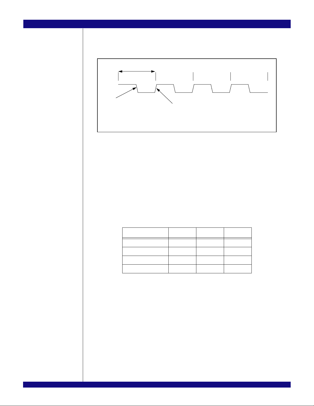
Throughout this manual, when describing signal transitions, the following terminology is used. Rising
edge indicates a low-to-high (0 to 1) transition. Falling edge indicates a high-to-low (1 to 0) transition. These
terms are illustrated in Figure 1.
Figure 1 Signal Transitions
Numeric Representations
To represent numerical values, either decimal, binary, or hexadecimal formats will be used. The binary
format is as follows: 0bDDD, where “D” represents either 0 or 1; the hexadecimal format is as follows:
0xDD, where “D” represents the hexadecimal digit(s); otherwise, it is decimal.
The compressed notation ABC[x|y|z]D refers to ABCxD, ABCyD, and ABCzD.
The compressed notation ABC[x..y]D refers to ABCxD, ABC(x+1)D, ABC(x+2)D,... ABCyD.
Data Units
The following data unit terminology is used in this document.
Term Words Bytes Bits
Byte 1/2 1 8
Word 1 2 16
Doubleword (Dword) 2 4 32
Quadword (Qword) 4 8 64
Table 1 Data Unit Terminology
In quadwords, bit 63 is always the most significant bit and bit 0 is the least significant bit. In doublewords, bit 31 is always the most significant bit and bit 0 is the least significant bit. In words, bit 15 is always
the most significant bit and bit 0 is the leas t significant bit. In bytes, bit 7 is always the most significant bit
and bit 0 is the least significant bit.
The ordering of bytes within words is referred to as either “big endian” or “little endian.” Big endian
systems label byte zero as the most significant (leftmost) byte of a word. Little endian systems label byte
zero as the least significant (rightmost) byte of a word. See Figure 2.
PES12T3G2 User Manual 2 January 28, 2013
Page 5

IDT
Notes
0 1 2 3
bit 0bit 31
Address of Bytes within Words: Big Endian
3 2 1 0
bit 0bit 31
Address of Bytes within Words: Little Endian
Figure 2 Example of Byte Ordering for “Big Endian” or “Little Endian” System Definition
Register Terminology
Software in the context of this register terminology refers to modifications made by PCIe root configuration writes to registers made through the slave SMBus interface or serial EEPROM register initialization.
See Table 2.
Type Abbreviation Description
Hardware Initialized HWINIT Register bits are initialized by firmware or hardware mechanisms
such as pin strapping or serial EEPROM. (System firmware hardware initialization is only allowed for system integrated devices.)
Bits are read-only after initialization and can only be reset (for
write-once by firmware) with reset.
Read Only and Clear RC Software can read the register/bits with this attribute. Reading the
value will automatically cause the register/bit to be reset to zero.
Writing to a RC location has no effect.
Read Clear and Write RCW Software can read the register/bits with this attribute. Reading the
value will automatically cause the register/bits to be reset to zero.
Writes cause the register/bits to be modified.
Reserved Reserved The value read from a reserved register/bit is undefined. Thus,
software must deal correctly with fields that are reserved. On
reads, software must use appropriate masks to extract the defined
bits and not rely on reserved bits being any particular value. On
writes, software must ensure that the values of reserved bit positions are preserved. That is, the values of reserved bit positions
must first be read, merged with the new values for other bit positions and then written back.
Read Only RO Software can only read registers/bits with this attribute. Contents
are hardwired to a constant value or are status bits that may be
set and cleared by hardware. Writing to a RO location has no
effect.
Read and Write RW Software can both read and write bits with this attribute.
Table 2 Register Terminology (Part 1 of 2)
PES12T3G2 User Manual 3 January 28, 2013
Page 6

IDT
Notes
Type Abbreviation Description
Read and Write Clear RW1C Software can read and write to registers/bits with this attribute.
However, writing a value of zero to a bit with this attribute has no
effect. A RW1C bit can only be set to a value of 1 by a hardware
event. To clear a RW1C bit (i.e., change its value to zero) a value
of one must be written to the location. An RW1C bit is never
cleared by hardware.
Read and Write when
Unlocked
Write Transient WT The zero is always read from a bit/field of this type. Writing of a
Zero Zero A zero register or bit must be written with a value of zero and
RWL Software can read the register/bits with this attribute. Writing to
register/bits with this attribute will only cause the value to be modified if the REGUNLOCK bit in the SWCNTL register is set. When
the REGUNLOCK bit is cleared, writes are ignored and the register/bits are effectively read-only
one is used to quality the writing of other bits/fields in the same
register.
returns a value of zero when read.
Table 2 Register Terminology (Part 2 of 2)
Use of Hypertext
In Chapter 8, Tables 8.2 and 8.3 contain register nam es and page numbers highlighted in blue under the
Register Definition column. In pdf files, users can jump from this source table directly to the registers by
clicking on the register name in the source table. Each register name in the table is linked directly to the
appropriate register in the register section of the chapter. To return to the source table after having jumped
to the register section, click on the same register name (in blue) in the register section.
Reference Documents
PCI Express Base Specification, Revision 1.1, PCI Special Interest Group.
PCI Power Management Interface Specification, Revision 1.1, PCI Special Interest Group.
PCI to PCI Bridge Architecture Specification, Revision 1.2, PCI Special Interest Group.
SMBus Specification, Revision 2.0.
Revision History
May 23, 2007: Initial publication of preliminaray user manual.
June 26, 2007: In Chapter 8, Configuration Registers, included only 3 registers with addresses in the
0x400-0x600 range. Updated Chapter 3, Link Operation.
July 11, 2007: Corrected AERUCS to AERUES in AERCTL register, Chapter 8. Added additional registers to Chapter 8 in the 0x400-0x600 range.
February 6, 2008: Added PMETOATIMER register to Chapter 8.
October 31, 2008: In Chapter 8, revised description L0SEL field in the PCIELCAP register and LDIS
field in the PCIELCTL register.
September 15, 2010: In Table 1.9, changed Buffer type for PCI Express from CML to PCIe differential
and changed reference clocks to HCSL
February 22, 2012: Added paragraph after Table 5.11 to explain use of DWord addresses.
January 28, 2013: In Figure 5.8, changed No-ack to Ack between DATALM and DATAUM.
PES12T3G2 User Manual 4 January 28, 2013
Page 7

Notes
Table of Contents
®
About This Manual
Introduction ....................................................................................................................................1
Content Summary ..........................................................................................................................1
Signal Nomenclature .....................................................................................................................1
Numeric Representations ..............................................................................................................2
Data Units ......................................................................................................................................2
Register Terminology .....................................................................................................................3
Use of Hypertext ............................................................................................................................4
Reference Documents ...................................................................................................................4
Revision History .............................................................................................................................4
PES12T3G2 Device Overview
Introduction.....................................................................................................................................1-1
Features..........................................................................................................................................1-1
System Diagram.............................................................................................................................1-2
Logic Diagram.................................................................................................................................1-3
System Identification.......................................................................................................................1-4
Vendor ID................................................................................................................................1-4
Device ID................................................................................................................................1-4
Revision ID.............................................................................................................................1-4
JTAG ID..................................................................................................................................1-4
Pin Description................................................................................................................................1-4
Pin Characteristics..........................................................................................................................1-9
Port Configuration.........................................................................................................................1-10
Clocking, Reset and Initialization
Clocking..........................................................................................................................................2-1
Initialization.....................................................................................................................................2-1
Reset...............................................................................................................................................2-2
Fundamental Reset................................................................................................................2-3
Hot Reset................................................................................................................................2-5
Upstream Secondary Bus Reset............................................................................................2-6
Downstream Secondary Bus Reset........................................................................................2-6
Downstream Port Reset Outputs....................................................................................................2-7
Power Enable Controlled Reset Output..................................................................................2-7
Power Good Controlled Reset Output....................................................................................2-8
Link Operation
Introduction.....................................................................................................................................3-1
Polarity Inversion............................................................................................................................3-1
Lane Reversal.................................................................................................................................3-1
Link Width Negotiation....................................................................................................................3-2
Dynamic Link Width Re-Configuration............................................................................................3-2
Background.............................................................................................................................3-2
Dynamic Link Width Re-Configuration Support in the PES12T3G2.......................................3-3
Link Speed Negotiation ...................................................................................................................3-3
Background.............................................................................................................................3-3
PES12T3G2 User Manual i January 28, 2013
Page 8

IDT Table of Contents
Notes
Link Speed Negotiation in the PES12T3G2 ...........................................................................3-4
Software Management of Link Speed ....................................................................................3-5
Link Retraining................................................................................................................................3-6
Slot Power Limit Support................................................................................................................3-6
Upstream Port ........................................................................................................................3-6
Downstream Port....................................................................................................................3-7
Link States......................................................................................................................................3-7
Active State Power Management ...................................................................................................3-8
Link Status......................................................................................................................................3-8
De-emphasis Negotiation ...............................................................................................................3-8
Low-Swing Transmitter Voltage Mode............................................................................................3-9
General Purpose I/O
Introduction.....................................................................................................................................4-1
GPIO Configuration ........................................................................................................................4-1
GPIO Pin Configured as an Input...........................................................................................4-1
GPIO Pin Configured as an Output........................................................................................4-2
GPIO Pin Configured as an Alternate Function......................................................................4-2
SMBus Interfaces
Introduction.....................................................................................................................................5-1
Master SMBus Interface.................................................................................................................5-2
Initialization.............................................................................................................................5-2
Serial EEPROM......................................................................................................................5-2
I/O Expanders.........................................................................................................................5-6
Slave SMBus Interface.................................................................................................................5-11
Initialization...........................................................................................................................5-11
SMBus Transactions ............................................................................................................5-12
Power Management
Introduction.....................................................................................................................................6-1
PME Messages...............................................................................................................................6-2
PCI-Express Power Management Fence Protocol.........................................................................6-2
Power Budgeting Capability............................................................................................................6-3
Hot-Plug and Hot-Swap
Hot-Plug..........................................................................................................................................7-1
Hot-Plug I/O Expander ...........................................................................................................7-4
Hot-Plug Interrupts and Wake-up...........................................................................................7-4
Legacy System Hot-Plug Support ..........................................................................................7-4
Hot-Swap........................................................................................................................................7-6
Configuration Registers
Configuration Space Organization..................................................................................................8-1
Upstream Port (Port 0) ...........................................................................................................8-3
Downstream Ports..................................................................................................................8-6
Register Definitions.......................................................................................................................8-10
Type 1 Configuration Header Registers...............................................................................8-10
PCI Express Capability Structure.........................................................................................8-19
Power Management Capability Structure.............................................................................8-34
Message Signaled Interrupt Capability Structure.................................................................8-36
Subsystem ID and Subsystem Vendor ID............................................................................8-37
PES12T3G2 User Manual ii January 28, 2013
Page 9

IDT Table of Contents
Notes
Extended Configuration Space Access Registers................................................................8-38
Advanced Error Reporting (AER) Enhanced Capability.......................................................8-39
Device Serial Number Enhanced Capability.........................................................................8-45
PCI Express Virtual Channel Capability...............................................................................8-46
Power Budgeting Enhanced Capability................................................................................8-52
Switch Status and Control Registers....................................................................................8-53
Physical Layer Control and Status Registers.......................................................................8-60
Power Management Control and Status Registers ..............................................................8-61
JTAG Boundary Scan
Introduction.....................................................................................................................................9-1
Test Access Point...........................................................................................................................9-1
Signal Definitions............................................................................................................................9-1
Boundary Scan Chain.....................................................................................................................9-3
Test Data Register (DR).................................................................................................................9-3
Boundary Scan Registers.......................................................................................................9-4
Instruction Register (IR)..................................................................................................................9-5
EXTEST..................................................................................................................................9-6
SAMPLE/PRELOAD...............................................................................................................9-6
BYPASS.................................................................................................................................9-6
CLAMP...................................................................................................................................9-7
IDCODE..................................................................................................................................9-7
VALIDATE..............................................................................................................................9-7
RESERVED............................................................................................................................9-7
Usage Considerations............................................................................................................9-7
PES12T3G2 User Manual iii January 28, 2013
Page 10

IDT Table of Contents
Notes
PES12T3G2 User Manual iv January 28, 2013
Page 11

Notes
List of Tables
®
Table 1.1 PES12T3G2 Device ID........................................................................................................1-4
Table 1.2 PES12T3G2 Revision ID.....................................................................................................1-4
Table 1.3 PCI Express Interface Pins..................................................................................................1-4
Table 1.4 SMBus Interface Pins..........................................................................................................1-5
Table 1.5 General Purpose I/O Pins....................................................................................................1-6
Table 1.6 System Pins.........................................................................................................................1-7
Table 1.7 Test Pins..............................................................................................................................1-7
Table 1.8 Power, Ground, and SerDes Resistor Pins.........................................................................1-8
Table 1.9 Pin Characteristics...............................................................................................................1-9
Table 2.1 Reference Clock Mode Encoding........................................................................................2-1
Table 2.2 Boot Configuration Vector Signals.......................................................................................2-2
Table 4.1 General Purpose I/O Pin Alternate Function.......................................................................4-1
Table 4.2 GPIO Pin Configuration.......................................................................................................4-1
Table 5.1 Serial EEPROM SMBus Address........................................................................................5-2
Table 5.2 PES12T3G2 Compatible Serial EEPROMs.........................................................................5-3
Table 5.3 Serial EEPROM Initialization Errors....................................................................................5-5
Table 5.4 I/O Expander Function Allocation........................................................................................5-6
Table 5.5 I/O Expander Default Output Signal Value..........................................................................5-7
Table 5.6 I/O Expander 0 Signals........................................................................................................5-9
Table 5.7 I/O Expander 2 Signals......................................................................................................5-10
Table 5.8 I/O Expander 4 Signals......................................................................................................5-10
Table 5.9 Slave SMBus Address When a Static Address is Selected...............................................5-11
Table 5.10 Slave SMBus Command Code Fields...............................................................................5-12
Table 5.11 CSR Register Read or Write Operation Byte Sequence...................................................5-13
Table 5.12 CSR Register Read or Write CMD Field Description.........................................................5-14
Table 5.13 Serial EEPROM Read or Write Operation Byte Sequence................................................5-14
Table 5.14 Serial EEPROM Read or Write CMD Field Description.....................................................5-15
Table 6.1 PES12T3G2 Power Management State Transition Diagram...............................................6-2
Table 7.1 Downstream Port Hot Plug Signals.....................................................................................7-3
Table 8.1 Base Addresses for Port Configuration Space Registers....................................................8-1
Table 8.2 Upstream Port 0 Configuration Space Registers.................................................................8-3
Table 8.3 Downstream Ports 2, 4, 6 Configuration Space Registers..................................................8-6
Table 9.1 JTAG Pin Descriptions.........................................................................................................9-2
Table 9.2 Boundary Scan Chain..........................................................................................................9-3
Table 9.3 Instructions Supported by PES12T3G2’s JTAG Boundary Scan........................................9-6
Table 9.4 System Controller Device Identification Register.................................................................9-7
PES12T3G2 User Manual v January 28, 2013
Page 12

IDT List of Tables
Notes
PES12T3G2 User Manual vi January 28, 2013
Page 13

Notes
List of Figures
®
Figure 1.1 PES12T3G2 Architectural Block Diagram ..........................................................................1-2
Figure 1.2 PES12T3G2 Logic Diagram ...............................................................................................1-3
Figure 1.3 PES12T3G2 Port & Device Numbering ...........................................................................1-10
Figure 2.1 Fundamental Reset with Serial EEPROM Initialization ......................................................2-4
Figure 2.2 Fundamental Reset Using RSTHALT to Keep Device in Quasi-Reset State .....................2-5
Figure 2.3 Power Enable Controlled Reset Output Mode Operation ..................................................2-7
Figure 2.4 Power Good Controlled Reset Output Mode Operation .....................................................2-8
Figure 3.1 Port Lane Reversal for Maximum Link Width of x4 (MAXLNKWDTH=0x4) .......................3-1
Figure 3.2 Port Lane Reversal for Maximum Link Width of x2 (MAXLNKWDTH=0x2) .......................3-2
Figure 3.3 PES12T3G2 ASPM Link Sate Transitions .........................................................................3-7
Figure 5.1 SMBus Interface Configuration Examples .........................................................................5-1
Figure 5.2 Single Double Word Initialization Sequence Format ..........................................................5-3
Figure 5.3 Sequential Double Word Initialization Sequence Format ...................................................5-4
Figure 5.4 Configuration Done Sequence Format ..............................................................................5-4
Figure 5.5 Slave SMBus Command Code Format ............................................................................5-12
Figure 5.6 CSR Register Read or Write CMD Field Format ..............................................................5-13
Figure 5.7 Serial EEPROM Read or Write CMD Field Format ..........................................................5-15
Figure 5.8 CSR Register Read Using SMBus Block Write/Read Transactions with PEC
Disabled ...........................................................................................................................5-16
Figure 5.9 Serial EEPROM Read Using SMBus Block Write/Read Transactions with PEC
Disabled ...........................................................................................................................5-16
Figure 5.10 CSR Register Write Using SMBus Block Write Transactions with PEC Disabled ...........5-16
Figure 5.11 Serial EEPROM Write Using SMBus Block Write Transactions with PEC Disabled ........5-17
Figure 5.12 Serial EEPROM Write Using SMBus Block Write Transactions with PEC Enabled ........5-17
Figure 5.13 CSR Register Read Using SMBus Read and Write Transactions with PEC Disabled ....5-17
Figure 6.1 PES12T3G2 Power Management State Transition Diagram .............................................6-1
Figure 7.1 Hot-Plug on Switch Downstream Slots Application ............................................................7-1
Figure 7.2 Hot-Plug with Switch on Add-In Card Application ..............................................................7-2
Figure 7.3 Hot-Plug with Carrier Card Application ..............................................................................7-2
Figure 7.4 PES12T3G2 Hot-Plug Event Signalling .............................................................................7-5
Figure 8.1 Port Configuration Space Organization .............................................................................8-2
Figure 9.1 Diagram of the JTAG Logic ................................................................................................9-1
Figure 9.2 State Diagram of PES12T3G2’s TAP Controller ................................................................9-2
Figure 9.3 Diagram of Observe-only Input Cell ...................................................................................9-4
Figure 9.4 Diagram of Output Cell ......................................................................................................9-4
Figure 9.5 Diagram of Bidirectional Cell ..............................................................................................9-5
Figure 9.6 Device ID Register Format .................................................................................................9-7
PES12T3G2 User Manual vii January 28, 2013
Page 14

IDT List of Figures
Notes
PES12T3G2 User Manual viii January 28, 2013
Page 15

Notes
Register List
®
AERCAP - AER Capabilities (0x100).....................................................................................................8-39
AERCEM - AER Correctable Error Mask (0x114).................................................................................. 8-44
AERCES - AER Correctable Error Status (0x110)................................................................................. 8-43
AERCTL - AER Control (0x118)............................................................................................................. 8-44
AERHL1DW - AER Header Log 1st Doubleword (0x11C)..................................................................... 8-45
AERHL2DW - AER Header Log 2nd Doubleword (0x120)..................................................................... 8-45
AERHL3DW - AER Header Log 3rd Doubleword (0x124)...................................................................... 8-45
AERHL4DW - AER Header Log 4th Doubleword (0x128)...................................................................... 8-45
AERUEM - AER Uncorrectable Error Mask (0x108).............................................................................. 8-40
AERUES - AER Uncorrectable Error Status (0x104).............................................................................8-39
AERUESV - AER Uncorrectable Error Severity (0x10C)........................................................................ 8-42
BAR0 - Base Address Register 0 (0x010).............................................................................................. 8-13
BAR1 - Base Address Register 1 (0x014).............................................................................................. 8-13
BCTL - Bridge Control Register (0x03E)................................................................................................8-18
BIST - Built-in Self Test Register (0x00F)..............................................................................................8-13
CAPPTR - Capabilities Pointer Register (0x034)................................................................................... 8-17
CCODE - Class Code Register (0x009).................................................................................................8-12
CLS - Cache Line Size Register (0x00C)............................................................................................... 8-12
DID - Device Identification Register (0x002)..........................................................................................8-10
ECFGADDR - Extended Configuration Space Access Address (0x0F8)...............................................8-38
ECFGDATA - Extended Configuration Space Access Data (0x0FC)..................................................... 8-38
EEPROMINTF - Serial EEPROM Interface (0x42C).............................................................................. 8-58
EROMBASE - Expansion ROM Base Address Register (0x038)........................................................... 8-17
GPECTL - General Purpose Event Control (0x450)............................................................................... 8-59
GPESTS - General Purpose Event Status (0x454)................................................................................ 8-60
GPIOCFG - General Purpose I/O Configuration (0x41C)....................................................................... 8-56
GPIOD - General Purpose I/O Data (0x420).......................................................................................... 8-57
GPIOFUNC - General Purpose I/O Control Function (0x418)................................................................ 8-56
HDR - Header Type Register (0x00E).................................................................................................... 8-13
HPCFGCTL - Hot-Plug Configuration Control (0x408)........................................................................... 8-55
INTRLINE - Interrupt Line Register (0x03C)........................................................................................... 8-18
INTRPIN - Interrupt PIN Register (0x03D).............................................................................................8-18
IOBASE - I/O Base Register (0x01C)..................................................................................................... 8-14
IOBASEU - I/O Base Upper Register (0x030)........................................................................................ 8-17
IOEXPADDR0 - SMBus I/O Expander Address 0 (0x434)..................................................................... 8-59
IOEXPADDR1 - SMBus I/O Expander Address 1 (0x438)..................................................................... 8-59
IOLIMIT - I/O Limit Register (0x01D)...................................................................................................... 8-14
IOLIMITU - I/O Limit Upper Register (0x032)......................................................................................... 8-17
MBASE - Memory Base Register (0x020).............................................................................................. 8-15
MLIMIT - Memory Limit Register (0x022)............................................................................................... 8-15
MSIADDR - Message Signaled Interrupt Address (0x0D4).................................................................... 8-37
MSICAP - Message Signaled Interrupt Capability and Control (0x0D0)................................................8-36
MSIMDATA - Message Signaled Interrupt Message Data (0x0DC)....................................................... 8-37
MSIUADDR - Message Signaled Interrupt Upper Address (0x0D8)......................................................8-37
PBUSN - Primary Bus Number Register (0x018)................................................................................... 8-13
PCICMD - PCI Command Register (0x004)...........................................................................................8-10
PCIECAP - PCI Express Capability (0x040)........................................................................................... 8-19
PCIEDCAP - PCI Express Device Capabilities (0x044).........................................................................8-20
PCIEDCAP2 - PCI Express Device Capabilities 2 (0x064)....................................................................8-31
PES12T3G2 User Manual ix January 28, 2013
Page 16

IDT Register List
Notes
PCIEDCTL - PCI Express Device Control (0x048)..................................................................................8-21
PCIEDCTL2 - PCI Express Device Control 2 (0x068).............................................................................8-31
PCIEDSTS - PCI Express Device Status (0x04A) ..................................................................................8-22
PCIEDSTS2 - PCI Express Device Status 2 (0x06A) .............................................................................8-32
PCIELCAP - PCI Express Link Capabilities (0x04C) ..............................................................................8-23
PCIELCAP2 - PCI Express Link Capabilities 2 (0x06C) .........................................................................8-32
PCIELCTL - PCI Express Link Control (0x050).......................................................................................8-24
PCIELCTL2 - PCI Express Link Control 2 (0x070)..................................................................................8-32
PCIELSTS - PCI Express Link Status (0x052)........................................................................................8-26
PCIELSTS2 - PCI Express Link Status 2 (0x072)...................................................................................8-34
PCIESCAP - PCI Express Slot Capabilities (0x054)...............................................................................8-27
PCIESCAP2 - PCI Express Slot Capabilities 2 (0x074)..........................................................................8-34
PCIESCTL - PCI Express Slot Control (0x058).......................................................................................8-29
PCIESCTL2 - PCI Express Slot Control 2 (0x078)..................................................................................8-34
PCIESSTS - PCI Express Slot Status (0x05A) .......................................................................................8-30
PCIESSTS2 - PCI Express Slot Status 2 (0x07A) ..................................................................................8-34
PCIEVCECAP - PCI Express VC Enhanced Capability Header (0x200)................................................8-46
PCISTS - PCI Status Register (0x006) ...................................................................................................8-11
PHYLSTATE0 - Phy Link State 0 (0x534)...............................................................................................8-61
PLTIMER - Primary Latency Timer (0x00D)............................................................................................8-12
PMBASE - Prefetchable Memory Base Register (0x024).......................................................................8-16
PMBASEU - Prefetchable Memory Base Upper Register (0x028)..........................................................8-16
PMCAP - PCI Power Management Capabilities (0x0C0)........................................................................8-34
PMCSR - PCI Power Management Control and Status (0x0C4) ............................................................8-35
PMETOATIMER - PME_TO_Ack Timer (0X708)....................................................................................8-61
PMLIMIT - Prefetchable Memory Limit Register (0x026)........................................................................8-16
PMLIMITU - Prefetchable Memory Limit Upper Register (0x02C)..........................................................8-17
PVCCAP1- Port VC Capability 1 (0x204)................................................................................................8-46
PVCCAP2- Port VC Capability 2 (0x208)................................................................................................8-47
PVCCTL - Port VC Control (0x20C)........................................................................................................8-47
PVCSTS - Port VC Status (0x20E) .........................................................................................................8-47
PWRBCAP - Power Budgeting Capabilities (0x280)...............................................................................8-52
PWRBD - Power Budgeting Data (0x288)...............................................................................................8-52
PWRBDSEL - Power Budgeting Data Select (0x284).............................................................................8-52
PWRBDV[7:0] - Power Budgeting Data Value [7:0] (0x300 - 0X31C).....................................................8-53
PWRBPBC - Power Budgeting Power Budget Capability (0x28C) .........................................................8-53
RID - Revision Identification Register (0x008) ........................................................................................8-12
SBUSN - Secondary Bus Number Register (0x019)...............................................................................8-13
SECSTS - Secondary Status Register (0x01E) ......................................................................................8-15
SERDESCTL- SerDes Control (0x500)...................................................................................................8-60
SLTIMER - Secondary Latency Timer Register (0x01B).........................................................................8-14
SMBUSCTL - SMBus Control (0x428)....................................................................................................8-58
SMBUSSTS - SMBus Status (0x424) .....................................................................................................8-57
SNUMCAP - Serial Number Capabilities (0x180) ...................................................................................8-45
SNUMLDW - Serial Number Lower Doubleword (0x184) .......................................................................8-45
SNUMUDW - Serial Number Upper Doubleword (0x188).......................................................................8-46
SSIDSSVID - Subsystem ID and Subsystem Vendor ID (0x0F4)...........................................................8-38
SSIDSSVIDCAP - Subsystem ID and Subsystem Vendor ID Capability (0x0F0)...................................8-37
SUBUSN - Subordinate Bus Number Register (0x01A)..........................................................................8-14
SWCTL - Switch Control (0x404)............................................................................................................8-54
SWSTS - Switch Status (0x400) .............................................................................................................8-53
VCR0CAP- VC Resource 0 Capability (0x210).......................................................................................8-48
VCR0CTL- VC Resource 0 Control (0x214)............................................................................................8-48
VCR0STS - VC Resource 0 Status (0x218)............................................................................................8-49
VCR0TBL0 - VC Resource 0 Arbitration Table Entry 0 (0x220)..............................................................8-50
PES12T3G2 User Manual x January 28, 2013
Page 17

IDT Register List
Notes
VCR0TBL1 - VC Resource 0 Arbitration Table Entry 1 (0x224)..............................................................8-50
VCR0TBL2 - VC Resource 0 Arbitration Table Entry 2 (0x228)..............................................................8-51
VCR0TBL3 - VC Resource 0 Arbitration Table Entry 3 (0x22C).............................................................8-51
VID - Vendor Identification Register (0x000)...........................................................................................8-10
PES12T3G2 User Manual xi January 28, 2013
Page 18

IDT Register List
Notes
PES12T3G2 User Manual xii January 28, 2013
Page 19

Notes
®
Chapter 1
PES12T3G2 Device Overview
Introduction
The 89HPES12T3G2 is a member of IDT’s PRECISE™ family of PCI Express® switching solutions. The
PES12T3G2 is a 12-lane, 3-port Gen2 peripheral chip that performs PCI Express Base switching with a
feature set optimized for high performance applications such as servers, storage, and communications/
networking. It provides connectivity and switching functions between a PCI Express upstream port and two
downstream ports and supports switching between downstream ports.
Features
High Performance PCI Express Switch
– Twelve 5 Gbps Gen2 PCI Express lanes
– Three switch ports
• One x4 upstream port
• Two x4 downstream ports
– Low latency cut-through switch architecture
– Support for Max Payload Size up to 2048 bytes
– One virtual channel
– Eight traffic classes
– PCI Express Base Specification Revision 2.0 compliant
Flexible Architecture with Numerous Configuration Options
– Automatic per port link width negotiation to x4, x2 or x1
– Automatic lane reversal on all ports
– Automatic polarity inversion
– Ability to load device configuration from serial EEPROM
Legacy Support
– PCI compatible INTx emulation
– Bus locking
Highly Integrated Solution
– Incorporates on-chip internal memory for packet buffering and queueing
– Integrates twelve 5 Gbps embedded SerDes with 8b/10b encoder/decoder (no separate trans-
ceivers needed)
• Receive equalization (RxEQ)
Reliability, Availability, and Serviceability (RAS) Features
– Internal end-to-end parity protection on all TLPs ensures data integrity even in systems that do
not implement end-to-end CRC (ECRC)
– Supports ECRC and Advanced Error Reporting
– Supports PCI Express Native Hot-Plug, Hot-Swap capable I/O
– Compatible with Hot-Plug I/O expanders used on PC motherboards
– Supports Hot-Swap
Power Management
– Utilizes advanced low-power design techniques to achieve low typical power consumption
– Support PCI Express Power Management Interface specification (PCI-PM 1.2)
– Supports PCI Express Active State Power Management (ASPM) link state
– Supports PCI Express Power Budgeting Capability
– Supports the optional PCI Express SerDes Transmit Low-Swing Voltage Mode
– Unused SerDes are disabled and can be powered-off
PES12T3G2 User Manual 1 - 1 January 28, 2013
Page 20
IDT PES12T3G2 Device Overview
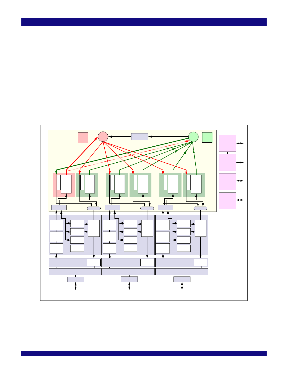
TDM Demux
D-Bus
U-Bus
ESP & Arb
ESP & Arb
ESP & Arb
ESP & Arb
ESP & Arb
ESP & Arb
Route Map
Table
Ingress
Processor
TLP
Checker
Egress
Processor
Completion
Processor
Message
Processor
TLP
Generator
Hot-Plug
Controller
Application Layer
Data Link Layer
Physical Layer & SerDes Mux/Demux
SerDes
Port 0
Port 2 Port 4
Switch Core
GPIO
Controller
Master
SMBus
Interface
Reset
Controller
Slave
SMBus
Interface
Output &
Replay Buffer
TDM Demux
Route Map
Table
Ingress
Processor
TLP
Checker
Egress
Processor
Completion
Processor
Message
Processor
TLP
Generator
Hot-Plug
Controller
Application Layer
Data Link Layer
Physical Layer & SerDes Mux/Demux
SerDes
Output &
Replay Buffer
TDM Demux
Route Map
Table
Ingress
Processor
TLP
Checker
Egress
Processor
Completion
Processor
Message
Processor
TLP
Generator
Hot-Plug
Controller
Application Layer
Data Link Layer
Physical Layer & SerDes Mux/Demux
SerDes
Output &
Replay Buffer
Input
Frame
Buffer
Input
Frame
Buffer
Input
Frame
Buffer
Input
Frame
Buffer
Input
Frame
Buffer
Input
Frame
Buffer
D-Bus
Arbiter
U-Bus
Arbiter
Bus Decoupler
Queue
Testability and Debug Features
– Built in Pseudo-Random Bit Stream (PRBS) generator
– Numerous SerDes test modes
– Ability to read and write any internal register via the SMBus
– Ability to bypass link training and force any link into any mode
– Provides statistics and performance counters
Nine General Purpose Input/Output Pins
– Each pin may be individually configured as an input or output
– Each pin may be individually configured as an interrupt input
– Some pins have selectable alternate functions
Packaged in a 19mm x 19mm, 324-ball BGA with 1mm
ball spacing
System Diagram
PES12T3G2 User Manual 1 - 2 January 28, 2013
Figure 1.1 PES12T3G2 Architectural Block Diagram
Page 21
IDT PES12T3G2 Device Overview
PE0TP[0]
Reference
Clocks
PEREFCLKP[0]
PEREFCLKN[0]
JTAG_TCK
GPIO[11,7:0]
9
General Purpose
I/O
VDDCORE
V
DD
I/O
V
DD
PEA
Power/Ground
MSMBADDR[4:1]
MSMBCLK
MSMBDAT
4
SSMBADDR[5,3:1]
SSMBCLK
SSMBDAT
4
Master
SMBus Interface
Slave
SMBus Interface
CCLKUS
RSTHALT
System
Pins
JTAG_TDI
JTAG_TDO
JTAG_TMS
JTAG_TRST_N
JTAG Pins
V
SS
SWMODE[2:0]
3
CCLKDS
PERSTN
REFCLKM
MSMBSMODE
PE0RP[0]
PE0RN[0]
PE0RP[3]
PE0RN[3]
PCI Express
Switch
SerDes Input
PE0TN[0]
PE0TP[3]
PE0TN[3]
PCI Express
Switch
SerDes Output
...
Port 0
Port 0
...
PE2RP[0]
PE2RN[0]
PE2RP[3]
PE2RN[3]
PCI Express
Switch
SerDes Input
PE2TP[0]
PE2TN[0]
PE2TP[3]
PE2TN[3]
PCI Express
Switch
SerDes Output
...
Port 2
Port 2
...
PE4RP[0]
PE4RN[0]
PE4RP[3]
PE4RN[3]
PCI Express
Switch
SerDes Input
PE4TP[0]
PE4TN[0]
PE4TP[3]
PE4TN[3]
PCI Express
Switch
SerDes Output
...
Port 4
Port 4
...
PES12T3G2
REFRES0
SerDes
Reference
Resistors
REFRES2
REFRES4
VDDPEHA
Reference Clock
Frequency Selection
VDDPETA
Logic Diagram
Figure 1.2 PES12T3G2 Logic Diagram
PES12T3G2 User Manual 1 - 3 January 28, 2013
Page 22

IDT PES12T3G2 Device Overview
Notes
System Identification
Vendor ID
All vendor ID fields in the device are hardwired to 0x111D which corresponds to Integrated Device Tech-
nology, Inc.
Device ID
The PES12T3G2 device ID is shown in Table 1.1.
Revisio n ID
The PES12T3G2 revision ID is shown in Table 1.2.
PCIe Device Device ID
0x1 0x8061
Table 1.1 PES12T3G2 Device ID
Revision ID Description
0x0 Corresponds to ZA silicon
0x1 Corresponds to ZB silicon
Table 1.2 PES12T3G2 Revision ID
JTAG ID
The JTAG ID is:
– Version: Same value as Revision ID. See Table 1.2
– Part number: Same value as base Device ID. See Table 1.1.
– Manufacturer ID: 0x33
– LSB: 0x1
Pin Description
The following tables list the functions of the pins provided on the PES12T3G2. S ome of the functions
listed may be multiplexed onto the same pin. The active polarity of a signal is defined using a suffix. Signals
ending with an “N” are defined as being active, or asserted, when at a logic zero (low) level. All other signals
(including clocks, buses, and select lines) will be interpreted as being active, or asserted, when at a logic
one (high) level.
Note: In the PES12T3G2, the two downstream ports are labeled port 2 and port 4.
Signal Type Name/Description
PE0RP[3:0]
PE0RN[3:0]
PE0TP[3:0]
PE0TN[3:0]
PE2RP[3:0]
PE2RN[3:0]
I PCI Express Port 0 Serial Data Receive. Differential PCI Express receive
pairs for port 0. Port 0 is the upstream port.
O PCI Express Port 0 Serial Data Transmit. Differential PCI Express trans-
mit pairs for port 0. Port 0 is the upstream port.
I PCI Express Port 2 Serial Data Receive. Differential PCI Express receive
pairs for port 2.
Table 1.3 PCI Express Interface Pins (Part 1 of 2)
PES12T3G2 User Manual 1 - 4 January 28, 2013
Page 23

IDT PES12T3G2 Device Overview
Notes
Signal Type Name/Description
PE2TP[3:0]
PE2TN[3:0]
PE4RP[3:0]
PE4RN[3:0]
PE4TP[3:0]
PE4TN[3:0]
PEREFCLKP[0]
PEREFCLKN[0]
REFCLKM I PCI Express Reference Clock Mode Select. This signal selects the fre-
Signal Type Name/Description
MSMBADDR[4:1] I Master SMBus Address. These pins determine the SMBus address of the
MSMBCLK I/O Master SMBus Clock. This bidirectional signal is used to synchronize
MSMBDAT I/O Master SMBus Data. This bidirectional signal is used for data on the mas-
SSMBADDR[5,3:1] I Slave SMBus Address. These pins determine the SMBus address to
SSMBCLK I/O Slave SMBus Clock. This bidirectional signal is used to synchronize trans-
SSMBDAT I/O Slave SMBus Data. This bidirectional signal is used for data on the slave
O PCI Express Port 2 Serial Data Transmit. Differential PCI Express trans-
mit pairs for port 2.
I PCI Express Port 4 Serial Data Receive. Differential PCI Express receive
pairs for port 4.
O PCI Express Port 4 Serial Data Transmit. Differential PCI Express trans-
mit pairs for port 4.
I PCI Express Reference Clock. Differential reference clock pair input. This
clock is used as the reference clock by on-chip PLLs to generate the clocks
required for the system logic and on-chip SerDes. The frequency of the differential reference clock is determined by the REFCLKM signal.
quency of the reference clock input.
0x0 - 100 MHz
0x1 - 125 MHz
This pin should be static and not change following the negation of
PERSTN.
Table 1.3 PCI Express Interface Pins (Part 2 of 2)
serial EEPROM from which configuration information is loaded.
transfers on the master SMBus.
ter SMBus.
which the slave SMBus interface responds.
fers on the slave SMBus.
SMBus.
Table 1.4 SMBus Interface Pins
PES12T3G2 User Manual 1 - 5 January 28, 2013
Page 24

IDT PES12T3G2 Device Overview
Notes
Signal Type Name/Description
GPIO[0] I/O General Purpose I/O.
GPIO[1] I/O General Purpose I/O.
GPIO[2] I/O General Purpose I/O.
GPIO[3] I/O General Purpose I/O.
GPIO[4] I/O General Purpose I/O.
GPIO[5] I/O General Purpose I/O.
GPIO[6] I/O General Purpose I/O.
GPIO[7] I/O General Purpose I/O.
GPIO[11] I/O General Purpose I/O.
This pin can be configured as a general purpose I/O pin.
Alternate function pin name: P2RSTN
Alternate function pin type: Output
Alternate function: Reset output for downstream port 2.
This pin can be configured as a general purpose I/O pin.
Alternate function pin name: P4RSTN
Alternate function pin type: Output
Alternate function: Reset output for downstream port 4.
This pin can be configured as a general purpose I/O pin.
Alternate function pin name: IOEXPINTN0
Alternate function pin type: Input
Alternate function: I/O expander interrupt 0 input.
This pin can be configured as a general purpose I/O pin.
This pin can be configured as a general purpose I/O pin.
Alternate function pin name: IOEXPINTN2
Alternate function pin type: Input
Alternate function: I/O Expander interrupt 2 input
This pin can be configured as a general purpose I/O pin.
This pin can be configured as a general purpose I/O pin.
This pin can be configured as a general purpose I/O pin.
Alternate function pin name: GPEN
Alternate function pin type: Output
Alternate function: General Purpose Event (GPE) output
This pin can be configured as a general purpose I/O pin.
Table 1.5 General Purpose I/O Pins
PES12T3G2 User Manual 1 - 6 January 28, 2013
Page 25

IDT PES12T3G2 Device Overview
Notes
Signal Type Name/Description
CCLKDS I Common Clock Downstream. The assertion of this pin indicates that all
CCLKUS I Common Clock Upstream. The assertion of this pin indicates that the
MSMBSMODE I Master SMBus Slow Mode. The assertion of this pin indicat es that th e
PERSTN I Fundamental Reset. Assertion of this signal resets all logic inside
RSTHALT I Reset Halt. When this signal is asserted during a PCI Express fundamental
SWMODE[2:0] I Switch Mode. These configuration pins determine the PES12T3G2 switch
downstream ports are using the same clock source as that provided to
downstream devices.This bit is used as the initial value of the Slot Clock
Configuration bit in all of the Link Status Registers for downstream ports.
The value may be overridden by modifying the SCLK bit in each downstream port’s PCIELSTS register.
upstream port is using the same clock source as the upstream device. This
bit is used as the initial value of the Slot Clock Configuration bit in the Link
Status Register for the upstream port. The value may be overridden by
modifying the SCLK bit in the P0_PCIELSTS register.
master SMBus should operate at 100 KHz instead of 400 KHz. This value
may not be overridden.
PES12T3G2 and initiates a PCI Express fundamental reset.
reset, PES12T3G2 executes the reset procedure and remains in a reset
state with the Master and Slave SMBuses active. This allows software to
read and write registers internal to the device before normal device operation begins. The device exits the reset state when the RSTHALT bit is
cleared in the SWCTL register by an SMBus master.
operating mode.
0x0 - Normal switch mode
0x1 - Normal switch mode with Serial EEPROM initialization
0x2 - through 0x7 Reserved
These pins should be static and not change following the negation of
PERSTN.
Table 1.6 System Pins
Signal Type Name/Description
JTAG_TCK I JTAG Clock. This is an input test clock used to clock the shifting of data
into or out of the boundary scan logic or JTAG Controller. JTAG_TCK is
independent of the system clock with a nominal 50% duty cycle.
JTAG_TDI I JTAG Data Input. This is the serial data input to the boundary scan logic or
JTAG Controller.
Table 1.7 Test Pins (Part 1 of 2)
PES12T3G2 User Manual 1 - 7 January 28, 2013
Page 26

IDT PES12T3G2 Device Overview
Notes
Signal Type Name/Description
JTAG_TDO O JTAG Data Output. This is the serial data shifted out from the boundary
JTAG_TMS I JTAG Mode. The value on this signal controls the test mode select of the
JTAG_TRST_N I JTAG Reset. This active low signal asynchronously resets the boundary
Signal Type Name/Description
REFRES0 I/O Port 0 External Reference Resistor. Provides a reference for the Port 0
REFRES2 I/O Port 2 External Reference Resistor. Provides a reference for the Port 2
REFRES4 I/O Port 4 External Reference Resistor. Provides a reference for the Port 4
V
DD
V
DD
V
DD
VDDPEHA I PCI Express Analog High Power. Serdes analog power supply (2.5V).
scan logic or JTAG Controller. When no data is being shifted out, this signal
is tri-stated.
boundary scan logic or JTAG Controller.
scan logic and JTAG TAP Controller. An external pull-up on the board is
recommended to meet the JTAG specification in cases where the tester
can access this signal. However, for systems running in functional mode,
one of the following should occur:
1) actively drive this signal low with control logic
2) statically drive this signal low with an external pull-down on the board
Table 1.7 Test Pins (Part 2 of 2)
SerDes bias currents and PLL calibration circuitry. A 3 kOhm +/- 1% resistor should be connected from this pin to ground.
SerDes bias currents and PLL calibration circuitry. A 3 kOhm +/- 1% resistor should be connected from this pin to ground.
SerDes bias currents and PLL calibration circuitry. A 3 kOhm +/- 1% resistor should be connected from this pin to ground.
CORE I Core V
I/O I I/O V
Power supply for core logic.
DD.
LVTTL I/O buffer power supply.
DD.
PEA I PCI Express Analog Power. Serdes analog power supply (1.0V).
V
PETA I PCI Express Transmitter Analog Voltage. Serdes transmitter analog
DD
power supply (1.0V).
V
SS
I Ground.
Table 1.8 Power, Ground, and SerDes Resistor Pins
PES12T3G2 User Manual 1 - 8 January 28, 2013
Page 27

IDT PES12T3G2 Device Overview
Notes
Pin Characteristics
Note: Some input pads of the PES12T3G2 do not contain internal pull-ups or pull-downs.
Unused inputs should be tied off to appropriate levels. This is especially critical for unused control
signal inputs which, if left floating, could adversely affect operation. Also, any input pin left floating
can cause a slight increase in power consumption.
2
I/O
Type
Serial Link
Input
High Drive
Function Pin Name Type Buffer
PCI Express
Interface
SMBus MSMBADDR[4:1
General
Purpose I/O
System Pins CCLKDS I LVTTL Input pull-up
PE0RN[3:0] I PCIe
PE0RP[3:0] I
PE0TN[3:0] O
PE0TP[3:0] O
PE2RN[3:0] I
PE2RP[3:0] I
PE2TN[3:0] O
PE2TP[3:0] O
PE4RN[3:0] I
PE4RP[3:0] I
PE4TN[3:0] O
PE4TP[3:0] O
PEREFCLKN[0] I HCSL Diff. Clock
PEREFCLKP[0] I
REFCLKM I LVTTL Input pull-down
]
MSMBCLK I/O STI
MSMBDAT I/O STI pull-up on board
SSMBADDR[5,3:
1]
SSMBCLK I/O STI pull-up on board
SSMBDAT I/O STI pull-up on board
GPIO[11,7:0] I/O LVTTL STI,
CCLKUS I Input pull-up
MSMBSMODE I Input pull-down
PERSTN I STI
RSTHALT I Input pull-down
SWMODE[2:0] I Input pull-down
Table 1.9 Pin Characteristics (Part 1 of 2)
differential
I LVTTL Input pull-up
I Input pull-up
Internal
Resistor
3
pull-up
1
Refer to Table 9
PES12T3G2
Data Sheet
pull-up on board
Notes
in the
PES12T3G2 User Manual 1 - 9 January 28, 2013
Page 28
IDT PES12T3G2 Device Overview
Notes
PES12T3G2
PCI to PCI
Bridge
PCI to PCI
Bridge
Dev. 2
PCI to PCI
Bridge
Dev. 4
Dev. 0
Port 0
Virtual PCI Bus
x4
Port 2
x4
Port 4
x4
Function Pin Name Type Buffer
I/O
Type
Internal
Resistor
Notes
1
EJTAG / JTAG JTAG_TCK I LVTTL STI pull-up
JTAG_TDI I STI pull-up
JTAG_TDO O
JTAG_TMS I STI pull-up
JTAG_TRST_N I STI pull-up
SerDes Reference Resistors
REFRES0 I/O Analog
REFRES2 I/O
REFRES4 I/O
Table 1.9 Pin Characteristics (Part 2 of 2)
1.
Internal resistor values under typical operating conditions are 92K Ω for pull-up and 90K Ω for pull-down.
2.
All receiver pins set the DC common mode voltage to ground. All transmitters must be AC coupled to the media.
3.
Schmitt Trigger Input (STI).
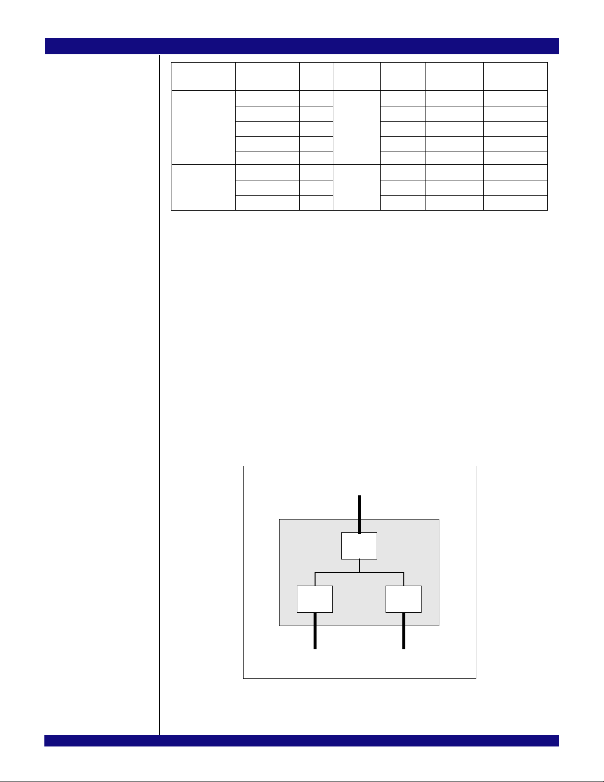
Port Configuration
The PES12T3G2 contains a total of three ports labeled 0, 2, and 4. Port 0 is always the upstream port.
Ports 2 and 4 are always downstream ports. All ports can operate at a maximum link width of x4, and all
ports support both 2.5 Gbps and 5.0 Gbps (Gen2). Per the PCIe specification, each switch port corresponds to a virtual PCI-PCI bridge device. In the PES12T3G2, device numbering follows port numbering.
Therefore, Port 0 corresponds to Device 0 on the upstream bus. Port 2 corresponds to Device 2 on the
PES12T3G2’s virtual PCI bus and Port 4 corresponds to Device 4.
Configuration read or write transactions to a non-existent device on the PES12T3G2’s virtual PCI bus
(i.e., Device 0, 1, 3, 5, etc.) are treated by the upstream port (port 0) as an unsupported request (i.e., the
device does not exist). Additionally, SMBus accesses to configuration registers of a non-existent device
have an undefined effect.
Figure 1.3 illustrates a diagram of Whitney with three x4 ports. The figure shows port and device
numbering.
Figure 1.3 PES12T3G2 Port & Device Numbering
PES12T3G2 User Manual 1 - 10 January 28, 2013
Page 29

Notes
®
Chapter 2
Clocking, Reset and
Initialization
Clocking
The PES12T3G2 has a single differential reference clock input (PEREFCLKP[0]/PEREFCLKN[0]) that is
used internally to generate all of the clocks required by the internal switch logic and the SerDes. The
frequency of the reference clock inputs may be selected by the Reference Clock Mode Select (REFCLKM)
input (see Table 2.1). All reference clock inputs must have the same frequency, as selected by REFCLKM.
REFCLKM Description
0 100 MHz reference clock input.
1 125 MHz reference clock input.
Table 2.1 Reference Clock Mode Encoding
Each PES12T3G2 port has an associated PLL. The reference clock differential inputs feed the on-chip
PLLs (one PLL per SerDes quad). Each PLL generates a 5.0 GHz internal SerDes clock which is used by
the four SerDes lanes in a SerDes quad. The PLL also produces a 250 MHz core clock, named PCLK. The
250 MHz PCLK output from the upstream port (i.e., Port 0) is used as the system clock for internal switch
logic. When the switch is placed in PLL Bypass test mode via the SWMODE pins, the 250 MHz clock generated by the PLL is bypassed and the reference clock input on PERE FCLKP[0]/PEREFCLKN[0] is used for
the core logic.
Initialization
A boot configuration vector consisting of the signals listed in Table 2.2 is sampled by the PES12T3G2
during a Fundamental Reset when PERSTN is negated
parameters for switch operation.
Since the boot configuration vector is sampled only during a Fundamental Reset sequence, the value of
signals which make up the boot configuration vector is ignored during other times and their state outside of
a Fundamental Reset has no effect on the operation of the PES12T3G2. While basic switch operation may
be configured using signals in the boot configuration vector, advanced switch features require configuration
via an external serial EEPROM. The external serial EEPROM allows modification of any bit in any software
visible register. See Chapter 5, SMBus Interfaces, for more information on the serial EEPROM.
The external serial EEPROM and slave SMBus interface may be used to override the function of some
of the signals in the boot configuration vector during a Fundamental Reset. The signals that may be overridden are noted in Table 2.2. The state of all of the boot configuration signals in Table 2.2 sampled during
the most recent Fundamental Reset may be determined by reading the SWSTS register.
. The boot configuration vector defines essential
PES12T3G2 User Manual 2 - 1 January 28, 2013
Page 30

IDT Clocking, Reset and Initialization
Notes
Signal
CCLKDS Y Com mon Cloc k Downstream. The assertion of this pin indicates
CCLKUS Y Com mon Cloc k Upstr ea m. The assertion of this pin indicates that
MSMBSMODE N Master SMBus Slow Mode. The assertion of this pin indi cates that
REFCLKM N PCI Express Reference Clock Mode Select. This signal selects
RSTHALT Y Reset Halt. When this signal is asserted during a PCI Express Fun-
SWMODE[2:0] N Switch Mode. These configuration pins determine the PES12T3G2
May Be
Overridden
Description
that all downstream ports are using the same clock source as that
provided to downstream devices.This pin is used as the initial value
of the Slot Clock Configuration bit in all of the Link Status Registers
for downstream ports. The value may be overridden by modifying
the SCLK bit in the downstream port’s PCIELSTS register.
the upstream port is using the same clock source as the upstream
device. This pin is used as the initial value of the Slot Clock Configuration bit in the Link Status Register for the upstream port. The value
may be overridden by modifying the SCLK bit in the downstream
port’s PCIELSTS register.
the master SMBus should operate at 100 KHz instead of 400 kHz.
the frequency of the reference clock input.
0x0 - 100 MHz
0x1 - 125 MHz
damental Reset, the PES12T3G2 executes the reset procedure and
remains in a reset state with the Master and Slave SMBuses active.
This allows software to read and write registers internal to the device
before normal device operation begins. The device exits the reset
state when the RSTHALT bit is cleared in the SWCTL register
through the SMBus.
The value may be overridden by modifying the RSTHALT bit in the
SWCTL register.
switch operating mode.
0x0 - Normal Switch Mode
0x1 - Normal Switch Mode with Serial EEPROM Initialization
0x2 through 0x7 - Reserved
Table 2.2 Boot Configuration Vector Signals
Reset
The PES12T3G2 defines four Conventional Reset categories: Fundamental reset, Hot Reset, Upstream
Secondary Bus Hot-Reset, and Downstream Secondary Bus Hot-Reset.
– A Fundamental Reset causes all logic in the PES12T3G2 to be returned to an initial state.
– A Hot Reset causes all logic in the PES12T3G2 to be returned to an initial state, but does not
cause the state of register fields denoted as “sticky” to be modified.
– An Upstream Secondary Bus Reset causes all devices on the virtual PCI bus to be hot reset
except the upstream port (i.e., upstream PCI to PCI bridge).
– A Downstream Secondary Bus Reset causes a hot reset to be propagated on the corresponding
external secondary bus link.
There are two sub-categories of Fundamental Reset: Cold reset and Warm reset. A Cold Reset occurs
following a device being powered on and assertion of PERSTN. A Warm Reset is a Fundamental Reset that
occurs without removal of power.
PES12T3G2 User Manual 2 - 2 January 28, 2013
Page 31

IDT Clocking, Reset and Initialization
Notes
Fundamental R eset
A Fundamental Reset may be initiated by any of the following conditions:
– A cold reset initiated by a power-on and the assertion of the PCI Express Reset (PERSTN) input
pin.
– A warm reset initiated by the assertion of the PCI Express Reset (PERSTN) input pin while power
is on.
– A warm reset initiated by the writing of a one to the Fundamental Reset (FRST) bit in the Switch
Control (SWCTL) register.
When configured to operate in normal mode, the following reset sequence is executed.
1. Wait for the Fundamental Reset condition to clear (e.g., negation of PERSTN). Note that PERSTN
must be asserted for at least 100 ms (Tpvperl) after the PES12T3G2 power supplies are stable, and
100µs (Tperst-clk) after the reference clock input is stable.
2. On negation of PERSTN, sample the boot configuration signals listed in Table 2.2. If PERSTN was
not asserted, use the previously sampled boot configuration signal values (e.g., when a Fundamental Reset is the result of setting the Fundamental Reset (FRST) bit in the Switch Control
(SWCTL) register).
• Examine the state of the sampled SWMODE[2:0] signals to determine the switch operating
mode.
3. The PLL and SerDes are initialized (i.e., PLL/CDR reset and lock).
4. Link training begins. While link training is in progress, proceed to step 5.
5. If the Reset Halt (RSTHALT) pin is asserted, the RSTHALT bit in the SWSTS register is set.
6. If the switch operating mode is not a test mode, then the reset signal to the PCI Express stacks and
associated logic is negated but they are held in a quasi-reset state in which the following actions
occur.
• All links enter an active link training state within 20 ms of the clearing of the Fundamental Reset
condition.
• Within 100 ms of the clearing of the Fundamental Reset condition, all of the stacks are able to
process configuration transactions and respond to these transactions with a configuration
request retry status completion. All other transactions are ignored.
7. The master SMBus operating frequency is determined.
• The state of the MSMBSMODE signal is examined. If it is asserted, then the master SM Bus is
initialized to operate at 100 KHz rather than 400 KHz.
8. The slave SMBus is taken out of reset and initialized. The slave SMBus address specified by the
SSMBADDR[5,3:1] pins is used.
9. The master SMBus is taken out of reset and initialized.
10. If the selected switch operating mode is one that requires initialization from the serial EEPROM, then
the contents of the serial EEPROM are read and the appropriate PES12T3G2 registers are updated.
• If a one is written by the serial EEPROM to the Full Link Retrain (FLRET) bit in any Phy Link
State 0 (PHYLSTATE0) register, then link retraining is initiated on the corresponding port using
the current link parameters.
• If an error is detected during loading of the serial EEPROM, then loading of the serial EEPROM
is aborted and the RSTHALT bit is set in the SWCTL register. Error information is recorded in
the SMBUSSTS register.
• When serial EEPROM initialization completes or when an error is detected, the EEPROM Done
(EEPROMDONE) bit in the SMBUSSTS register is set.
• If the RSTHALT bit is set in the SWCTL register, proceed to step 11. Else, proceed to step 12.
11. If the Reset Halt (RSTHALT) bit is set in the SWCTL register, all of the logic is held in a reset state
except the master and slave SMBuses, the control/status registers, and the stacks which continue
to be held in a quasi-reset state and respond to configuration transactions with a retry. The device
PES12T3G2 User Manual 2 - 3 January 28, 2013
Page 32

IDT Clocking, Reset and Initialization
Notes
PExREFCLKP/N
Vdd
PERSTN
SerDes
Master SMBus
Slave SMBus
Tpvperl
CDR Reset & Lock
Ready for Normal Operation
Ready for Normal Operation
Ready
Idle
Serial EEPROM Initialization
Notes:
20 ms max.
Stacks held in Quasi-Reset Mode
Link Training
PLL Lock
Tperst-clk
1) Reference Clock (REFCLK) not shown to scale.
2) The PES12T3G2 requires a minimum time for Tperst-clk of 1µs. The PES12T3G2 requires a minimum time for Tpvperl of 1ms.
3) In a system, the values of Tpvperl and Tperst-clk depend on the mechanical form factor in which the PES12T3G2 is used. For example,
the PCIe Card Electromechanical Specification, Revision 2.0, specifies minimum values of Tperst-clk=100µs and Tpvperl=100ms.
1ms max
remains in this state until the RSTHALT bit is cleared via the slave SMBus. In this mode, an external
agent may read and write any internal control and status registers and may access the external
serial EEPROM via the EEPROMINTF register.
12. Normal device operation begins.
The PCIe 2.0 specification indicates that a device must respond to Configuration Request transactions
within 100 ms from the end of Conventional Reset (cold, warm, or hot). A dditionally, the PCIe specification
indicates that a device must respond to Configuration Requests with a Successful Completion wi thin 1.0
second after Conventional Reset of a device. The reset sequence above guarantees that the PES12T3G2
will be ready to respond successfully to configuration request within the 1.0 second period as long as the
serial EEPROM initialization process completes within 200 ms. During EEPROM initialization, the
PES12T3G2 responds to a Configuration Request with Configuration-Request-Retry-Status Completion.
Under normal circumstances, 200 ms is more than adequate to initialize registers in the device even with a
Master SMBus operating frequency of 100 KHz.
Serial EEPROM initialization may cause writes to register fiel ds that initiate side effects such as link
retraining. These side effects are initiated at the point at which the write occurs. Therefore, serial EEPROM
initialization should be structured in a manner so as to ensure proper configuration prior to initiation of these
side effects.
A warm reset initiated by a configuration request writing a one to the Fundamental Reset (FRST) bit in
the Switch Control (SWCTL) register always results in the PES12T3G2 returning a Successful Completion
to the requester before the warm reset process begins.
The PES12T3G2 provides a reset output signal for each downstream port implemented as a GPIO alternate function. When a Fundamental Reset occurs, all of the GPIO pins default to GPIO inputs. Therefore,
the downstream port resets are tri-stated. A system designer should use a pull-down on these signals if
they are used as reset outputs.
The operation of a Fundamental Reset with serial EEPROM initialization (i.e., SWMODE [2:0] = 0x1) is
illustrated in Figure 2.1.
Figure 2.1 Fundamental Reset with Serial EEPROM Initialization
PES12T3G2 User Manual 2 - 4 January 28, 2013
The operation of a Fundamental Reset using RSTHALT is illustrated in Figure 2.2.
Page 33

IDT Clocking, Reset and Initialization
Notes
SerDes
Slave SMBus
CDR Reset & Lock
Ready for Normal Operation
Ready for Normal Operation
Notes:
1ms max
20 ms max.
Stacks held i n Q u asi-Reset Mo de
Link Training
PLL Lock
RSTHALT
RSTHALT bit in SWCTL register is set
RSTH ALT bit in S WCTL c leared ( i.e., by slave SM Bus)
PExREFCLKP/N
Vdd
PERSTN
Tpvperl
Tperst-clk
1) Reference Clock (REFCLK) not shown to scale.
2) The PES12T3G2 requires a minimum time for Tperst-clk of 1µs. The PES12T3G2 requires a minimum time for Tpvperl of 1ms.
3) In a system, the values of Tpvperl and Tperst-clk depend on the mechanical form factor in which the PES12T3G2 is used. For example,
the PCIe Card Electromechanical Specification, Revision 2.0, specifies minimum values of Tperst-clk=100µs and Tpvperl=100ms.
Figure 2.2 Fundamental Reset Using RSTHALT to Keep Device in Quasi-Reset State
Hot Reset
A hot reset may be initiated by any of the following conditions:
– Reception of TS1 ordered-sets on the upstream port indicating a hot reset.
– Data link layer of the upstream port transitions to the DL_Down state.
– Writing a one to the Hot Reset (HRST) bit in the Switch Control (SWCTL) register.
The initiation of a hot reset due to the data l ink layer of the upstream port transitioning to the DL_D own
state may be disabled by setting the Disable Link Down Hot Reset (DLDHRST) bit in the Switch Control
(SWCTL) register. Other hot reset conditions are unaffected by this bit.
When a hot reset occurs, the following sequence is executed.
1. Each downstream port whose link is up propagates the hot reset by transmitting TS1 ordered sets
with the hot reset bit set.
2. All of the logic associated with the PES12T3G2 except the PLLs, SerDes, master SMBus interface,
and slave SMBus interface is reset.
3. All registers fields in all registers, except those denoted as “sticky” or Read and Write when Unlocked
(i.e, RWL), are reset to their initial value. The value of fields denoted as “sticky” or RWL is preserved
across a hot reset.
4. Link training begins. While link training is in progress, proceed to step 5.
5. The PCI Express stacks and associated logic are held in a quasi-reset state in which the following
actions occur.
– All links enter an active link training state within 20 ms of the clearing of the hot reset condition.
– Within 100 ms of the clearing of the Hot Reset condition, all of the stacks are able to process
configuration transactions and respond to these transactions with a configuration request retry
status completion. All other transactions are ignored.
6. If the selected switch operating mode is one that requires initialization from the serial EEPROM and
the Disable Hot Reset Serial EEPROM Initialization (DHRSTSEI) bit is not set in the Switch Control
(SWCTL) register, then the contents of the serial EEPROM are read and the appropriate
PES12T3G2 registers are updated.
PES12T3G2 User Manual 2 - 5 January 28, 2013
Page 34

IDT Clocking, Reset and Initialization
Notes
• If a one is written by the serial EEPROM to the Full Link Retrain (FLRET) bit in any Phy Link
State 0 (PHYLSTATE0) register, then link retraining is initiated on the corresponding port using
the current link parameters.
• If an error is detected during loading of the serial EEPROM, then loading of the serial EEPROM
is aborted and the RSTHALT bit is set in the SWCTL register. Error information is recorded in
the SMBUSSTS register.
• When serial EEPROM initialization completes or when an error is detected, the DONE bit in the
SMBUSSTS register is set.
7. If the Reset Halt (RSTHALT) bit is set in the SWCTL register, all of the logic is held in a reset state
except the master and slave SMBuses. The RSTHALT bit is only set if serial EEPROM initialization
is enabled in step 6.
8. Normal device operation begins.
The operation of the slave SMBus interface is unaffected by a hot reset. Using the slave SMBus to
access a register that is reset by a hot reset causes zero to be returned on a read and written data to be
ignored on writes.
A hot reset initiated by the writing of a one to the Hot Reset (HRS T) bit in the S witch Control (SWCTL)
register always results in the PES12T3G2 returning a completion
process begins. Additionally, the upstream link is fully retrained (i.e., the upstream LTSSM transitions to the
Detect state).
Upstream Secondary Bus Reset
An Upstream Secondary Bus Reset may be initiated by the following condition:
– A one is written to the Secondary Bus Reset (SRESET) bit in the upstream port’s (i.e., port 0)
Bridge Control Register (BCTL).
When an Upstream Secondary Bus Reset occurs, the following sequence is executed.
to the requester before the hot reset
1. Each downstream port whose link is up propagates the reset by transmitting TS1 ordered sets with
the hot reset bit set.
2. All registers fields in all registers associated with downstream ports, except those denoted as “sticky”
or Read and Write when Unlocked (i.e, RWL), are reset to their initial value. The value of fields
denoted as “sticky” or RWL is unaffected by an Upstream Secondary Bus Reset.
3. All TLPs received from downstream ports and queued in the PES12T3G2 are discarded.
4. Logic in the stack, application layer and switch core associated with the downstream ports are gracefully reset.
5. Wait for software to clear the Secondary Bus Reset (SRESET) bit in the upstream port’s Bridge
Control Register (BCTL).
6. Normal downstream port operation begins.
The operation of the upstream port is unaffected by a secondary bus reset. The link remains up and
Type 0 configuration read and write transactions that target the upstream port complete normally.
During an Upstream Secondary Bus Reset, all TLPs destined to the secondary side of the upstream
port’s PCI-to-PCI bridge are treated in an undefined manner. The user should ensure no TLPs are sent to
the secondary side of the upstream port’s PCI-to-PCI bridge until the SRESET bit in the BCTL register is
cleared.
The operation of the slave SMBus interface is unaffected by an Upstream Secondary Bus Reset. Using
the slave SMBus to access a register that is reset by an Upstream Secondary Bus Reset causes the
register’s default value to be returned on a read and written data to be ignored on writes.
Downstream Secondary Bus Reset
A Downstream Secondary Bus Reset may be initiated by the following condition:
– A one is written to the Secondary Bus Reset (SRESET) bit in a downstream port’s Bridge Control
Register (BCTL).
PES12T3G2 User Manual 2 - 6 January 28, 2013
Page 35

IDT Clocking, Reset and Initialization
Notes
PxPEP
PxRSTN
T
PWR2RST
T
RST2PWR
When a Downstream Secondary Bus Reset occurs, the following sequence is executed.
1. If the corresponding downstream port’s link is up, TS1 ordered sets with the hot reset bit set are
transmitted
2. All TLPs received from corresponding downstream port and queued in the PES12T3G2 are
discarded.
3. Wait for software to clear the Secondary Bus Reset (SRESET) bit in the upstream port’s Bridge
Control Register (BCTL).
4. Normal downstream port operation begins.
The operation of the upstream port is unaffected by a Downstream Secondary Bus Reset.
The operation of other downstream ports is unaffected by a Downstream Secondary Bus Reset.
During a Downstream Secondary Bus Reset, Type 0 configuration read and write transactions that
target the downstream port complete normally.
During a Downstream Secondary Bus Reset, all TLPs destined to the secondary side of the downstream
port’s PCI-to-PCI bridge are treated as unsupported requests.
The operation of the slave SMBus interface is unaffected by a Downstream Secondary Bus Reset.
Downstream Port Reset Outputs
Individual downstream port reset outputs (P2RSTN and P4RSTN ) are provided as GPIO pin alternate
functions. Following a Fundamental Reset, all of the GPIO pins default to GPIO inputs. Therefore, the
downstream port resets are tri-stated. A system designer should use a pull-down on these signals if they
are used as reset outputs.
The PES12T3G2 ensures through hardware that the minimum PxRSTN assertion pulse width is no less
than 200 µ s. Downstream port reset outputs can be configured to operate in one of two modes. These
modes are power enable controlled reset output and power good controlled reset output. The downstream
port reset output mode is determined by the Reset Mode (RSTMODE) field in the Hot-Plug Configuration
Control (HPCFGCTL) register.
Power Enable Controlled Reset Output
In this mode a downstream port reset output state is controlled as a side effect of slot power being
turned on or off. The operation of this mode is illustrated in Figure 2.3. A downstream port’s slot power is
controlled by the Power Controller Control (PCC) bit in the PCI Express Slot Control (PCIESCTL) register
Figure 2.3 Power Enable Controlled Reset Output Mode Operation
While slot power is disabled, the corresponding downstream port reset output is asserted. When slot
power is enabled by writing a zero to the PCC bit, the Port x Power Enable Output (PxPEP) is asserted and
then power to the slot is enabled and the corresponding downstream port reset output is negated. The time
between the assertion of the PxPEP signal and the negation of the PxRSTN signal is controlled by the
value in the Slot Power to Reset Negation (PWR2RST) field in the HPCFGCTL register. While slot power is
enabled, the corresponding downstream port reset output is negated.
PES12T3G2 User Manual 2 - 7 January 28, 2013
Page 36

IDT Clocking, Reset and Initialization
Notes
PxPEP
PxPWRGDN
T
PWR2RST
PxRSTN
T
RST2PWR
When slot power is disabled by writing a one to the PCC bit, the corresponding downstream port reset
output is asserted and then slot power is disabled. The time between the assertion of the PxRSTN signal
and the negation of the PxPEP signal is controlled by the value in the Reset Negation to Slot Power
(RST2PWR) field in the HPCFGCTL register.
Power Good Controlled Reset Output
As in the Power Enable Controlled Reset mode, in this mode a downstream port reset output state is
controlled as a side effect of slot power being turned on or off. However, the timing in this mode depends on
the power good state of the slot’s power supply. The operation of this mode is illustrated in Figure 2.4.
The operation of this mode is similar to that of the Power Enable Controlled Reset mode except that
when power is enabled, the negation of the corresponding port reset output occurs as a result of and after
assertion of the slot’s Power Good (PxPWRGDN) signal is observed. The time between the assertion of the
PxPWRGDN signal and the negation of the PxRSTN signal is controlled by the value in the Slot Power to
Reset Negation (PWR2RST) field in the HPCFGCTL register.
Figure 2.4 Power Good Controlled Reset Output Mode Operation
When slot power is disabled by writing a one to the PCC bit, the corresponding downstream port reset
output is asserted and then slot power is disabled. The time between the assertion of the PxRSTN signal
and the negation of the PxPEP signal is controlled by the value in the Reset Negation to Slot Power
(RST2PWR) field in the HPCFGCTL register.
If at any point while a downstream port is not being reset (i.e., PxRSTN is negated) a power fault is
detected (i.e., PxPWRGDN is negated), then the corresponding port reset output is immediately asserted.
Since the PxPWRGDN signal is an I/O expander input, it may not be possible to meet a profile’s power level
invalid to reset asserted timing specification (i.e., PxPWRGDN to PxRSTN). Systems that require a shorter
time interval may implement this functionality external to the PES12T3G2.
PES12T3G2 User Manual 2 - 8 January 28, 2013
Page 37

Notes
®
Chapter 3
PExRP[0]
PExRP[1]
PExRP[2]
PExRP[3]
PES12T3G2
lane 0
lane 1
lane 2
lane 3
(a) x4 Port without lane reversal
PExRP[0]
PExRP[1]
PExRP[2]
PExRP[3]
PES12T3G2
lane 3
lane 2
lane 1
lane 0
(b) x4 Port with lane reversal
PExRP[0]
PExRP[1]
PExRP[2]
PExRP[3]
PES12T3G2
lane 0
lane 1
(a) x2 Port without lane reversal
PExRP[0]
PExRP[1]
PExRP[2]
PExRP[3]
PES12T3G2
lane 1
lane 0
(b) x2 Port with lane reversal
PExRP[0]
PExRP[1]
PExRP[2]
PExRP[3]
PES12T3G2
lane 0
(a) x1 Port without lane reversal
PExRP[0]
PExRP[1]
PExRP[2]
PExRP[3]
PES12T3G2
lane 0
(b) x1 Port with lane reversal
Link Operation
Introduction
Link operation in the PES12T3G2 adheres to the PCI Express 2.0 Base Specification, supporting
speeds of 2.5 Gbps and 5.0 Gbps. The PES12T3G2 contains four ports. All ports operate with a maximum
link width of x4. The SerDes lanes are statically assigned to a port.
Polarity Inversion
Each port of the PES12T3G2 supports automatic polarity inversion as required by the PCIe specification. Polarity inversion is a function of the receiver and not the transmitter. The transmitter never inverts its
data. During link training, the receiver examines symbols 6 through 15 of the TS1 and TS2 ordered sets for
inversion of the PExRP[n] and PExRN[n] signals. If an inversion is detected, then logic for the receiving
lane automatically inverts received data. Polarity inversion is a lane and not a l ink function. Therefore, it is
possible for some lanes of link to be inverted and for others not to be inverted.
Lane Reversal
The PCIe specification describes an optional lane reversal feature. The PES12T3G2 supports the automatic lane reversal feature outlined in the PCIe specification. The operation of lane reversal is dependent
on the maximum link width selected by the MAXLNKWDTH field in the PCI Express Link Capabilities
(PCIELCAP) register. Lane reversal mapping for the various non-trivial x4 port maximum link width configurations supported by the PES12T3G2 are illustrated in Figures 3.1 and 3.2.
PES12T3G2 User Manual 3 - 1 January 28, 2013
Figure 3.1 Port Lane Reversal for Maximum Link Width of x4 (MAXLNKWDTH=0x4)
Page 38

IDT Link Operation
Notes
PExRP[0]
PExRP[1]
PExRP[2]
PExRP[3]
PES12T3G2
lane 0
lane 1
(a) x2 Port without lane reversal
PExRP[0]
PExRP[1]
PExRP[2]
PExRP[3]
PES12T3G2
lane 1
lane 0
(b) x2 Port with lane reversal
PExRP[0]
PExRP[1]
PExRP[2]
PExRP[3]
PES12T3G2
lane 0
(c) x1 Port without lane reversal
PExRP[0]
PExRP[1]
PExRP[2]
PExRP[3]
PES12T3G2
lane 0
(d) x1 Port with lane reversal
Figure 3.2 Port Lane Reversal for Maximum Link Width of x2 (MAXLNKWDTH=0x2)
Link Width Negotiation
The PES12T3G2 supports the optional link variable width negotiation feature outlined in the PCIe 2.0
specification. The maximum port link width is discussed in section Port Configuration on page 1-10. The
actual link width is determined dynamically during link training. Ports limited to a maximum link width of x4
are capable of negotiating to a x4, x2, or x1 link width.
The negotiated width of each link after a full link train
Width (NLW) field in the corresponding port’s PCIe Link Status (PCIELSTS) register. This field indicates the
actual link width at the time the field is read.
1
may be determined from the Negotiated Link
The Maximum Link Width (MAXLNKWDTH) field in a port’s PCI Express Link Capabilities (PCIELCAP)
register contains the maximum link width of the port. This field is of RWL type and may be modified when
the REGUNLOCK bit is set in the SWCTL register. Modification of this field allows the maximum link width
of the port to be configured. The new link width takes effect the next time full link training occurs.
When a x4 port negotiates to a width less than x4, the unused SerDes lanes are put in a low power
state. When a port is disabled, all SerDes lanes associated with that port are powered down.
Dynamic Link Width Re-Configuration
Background
The PCI Express 2.0 specification includes support for dynamic upconfiguration of link wi dths. This
optional capability allows both components of a link to dynamically downconfigure & upconfigure links
based on implementation specific criteria such as power savings, link bandwidth requirements, or link reliability problems.
As an example, a link that initially does a full link train to x4 may be dynamically downconfigured to x1 in
order to save power when there is little traffic on the link. As traffic increases, the link may be dynamically
upconfigured to its initial link width of x4. Also, the link width may be downconfigured if a particular lane is
determined to be unreliable.
With dynamic link width re-configuration, the system designer can choose to connect components with
enough lanes to handle worst case bandwidth requirements, yet not waste power when the link is not fully
utilized. This capability offers an additional mechanism for link power reduction on top of the traditional
ASPM link states (L0s, L1, etc.)
1.
A full link train is a link training in which the LTSSM transitions through the Detect state.
PES12T3G2 User Manual 3 - 2 January 28, 2013
Page 39

IDT Link Operation
Notes
Dynamic upconfiguration and downconfiguration is done on a per-link basis, and does not result in the
link going into a DL_Down state. A link can be downconfigured down to x1. A link can be upconfigured up to
the negotiated link width set after a full link train. For example, a link that trained to a width of x2 after a full
link train cannot be upconfigured to a width above x2.
When a link is downconfigured to a smaller width, inactive lanes are kept in Electrical Idle with their
receiver terminations enabled. These lanes continue to be associated with the downconfigured port’s
LTSSM. In order for upconfiguration to occur successfully, both of the link components must support it.
Furthermore, the PCIe specification recommends that a link component not initiate downconfiguration
unless the link partner supports link upconfiguration, except for link reliability reasons.
The capability to upconfigure a link is transmitted among components using the in-band TS2 ordered
set. When downconfiguration or upconfiguration of the link width occurs, one of the components on the link
initiates the process, while the other component responds to the process. The PCIe specification indicates
that both of these capabilities are optional.
Software may be notified of link width re-configuration via the link bandwidth notification mechanism
described in the PCIe 2.0 specification. This mechanism is enabled by setting the Link Bandwidth Management Interrupt Enable (LBWINTEN) bit in the PCIELCTL register of switch downstream ports. Software can
prevent a device from initiating link width re-configuration for reasons other than reliability by setting the
Hardware Autonomous Width Disable (HAWD) bit in the port’s Link Control Register (PCIELCTL). Note that
the HAWD bit does not prevent a device from re-configuring the link width in response to link partner
requests.
Dynamic Link Width Re-Confi gu ra tion Support in the PES12T3G2
The PES12T3G2 supports dynamic link width upconfiguration and down-configuration in response to
link partner requests. The PES12T3G2 ports do not autonomously initiate link width upconfiguration and
downconfiguration of links. Therefore, the Hardware Autonomous Width Disable (HAWD) bit in the port’s
PCIELCTL register has no effect and is hardwired to 0x0. Additionally, the PES12T3G2 port’s never set the
‘Autonomous Change’ bit in the training sets exchanged with the link partner during link training. Still, a link
partner connected to a PES12T3G2 downstream port may autonomously change link width. When this
occurs, the PES12T3G2 downstream port sets the Link Autonomous Bandwidth Status (LABWSTS) bit in
the PCIELSTS register.
Link Speed Negotiation
Background
The PCIe 2.0 specification introduces support for 5.0 Gbps data rates per lane (a.k.a., Gen2), in addition
to the 2.5 Gbps data rates (a.k.a, Gen1) mandated in previous versions of the specification. The PCIe spec
indicates that Gen2 support is optional while Gen1 support is mandatory.
All lanes of a link must operate at the same data rate. During full link training (i.e., from th e Detect state),
links initially operate at 2.5 Gbps. Once the PHY Link Training State Machine (LTSSM) on both components
of the link reach the L0 state, the link speed may be upgraded to 5.0 Gbps if this capability is advertised by
both components. The process of upgrading the link speed does not result in a DL_Down state.
A component advertises its supported speeds via the Data Rate Identifier bits in the TS1 and TS2
training sets transmitted to its link partner during link training. The PCIe spec permits a component to
change its supported speeds dynamically. It is allowed for a component to advertise supported link speeds
without necessarily changing the link speed, via the Recovery LTSSM state.
A component determines the supported speeds of its link partner by examining the Data Rate Identifier
bits in the TS1/TS2 training sets received during link training, specifically in the Configuration.Complete and
Recovery.RcvrCfg states. The latest advertisement received overrides any previously recorded value.
PES12T3G2 User Manual 3 - 3 January 28, 2013
Page 40

IDT Link Operation
Notes
It is the responsibility of the upstream component of the link (i.e., switch downstream ports) to keep the
link at the target link speed or at the highest common speed supported by both components of the link,
whichever is lower. Either link component may request a link speed change due to the following:
– Software commands via the Link Control registers (PCIELCTL and PCIELCTL2)
– Autonomous (i.e., implementation specific) mechanisms
– Link reliability reasons (i.e., speed downgrade).
A component must not initiate a link speed upgrade if it has never recorded support for the higher speed
by its link partner since the last time the component exited the Detect state. Therefore, if a Gen2 capable
component link-trains with a Gen1 only component, the Gen2 capable component will not request a link
speed upgrade.
A component may initiate a link speed change if it has recorded support for the target speed by its link
partner since exiting the Detect state. The link speed change operation via the Recovery state may succeed
or fail, depending on the link partner’s current support for the target speed as well as the link reliability at
that speed. If it fails, the initiating component must wait 200ms before re-trying to upgrade the speed, or
until the link partner advertises support for the higher speed.
The upstream component must initiate a link speed upgrade if it has recorded support for the higher
speed by its link partner since exit from the Detect state, and software sets the Link Retrain bit in the
PCIELCTL register with a target link speed which is not equal to the current link speed. Additionally, the
upstream component (i.e., switch downstream port) is capable of notifying software of link speed changes
via the Link Bandwidth Notification mechanism described in the PCIe 2.0 specification.
Link Speed Negotiation in the PES12T3G2
The PES12T3G2 ports support per lane data rates of 5.0 Gbps and 2.5 Gbps. The highest data rate of
each link is determined dynamically, and depends on the following factors:
– Maximum link data rate supported by both components of the link
– The Target Link Speed se t via the Link Control 2 Register (PCIELCTL2)
– The reliability of the link at 5.0 Gbps
By default, the Target Link Speed (TLS) of each port is set to 5.0 Gbps. Therefore, the PES12T3G2
ports advertise support for 2.5 Gbps and 5.0 Gbps during the link training process vi a training-sets. After a
fundamental reset, each port link trains to the L0 state at 2.5 Gbps. If the Target Link Speed indicates 5.0
Gbps (default value), the PHY LTSSM automatically initiates link speed upgrade to 5.0 Gbps using the link
speed change mechanism described in the PCIe 2.0 specification. This behavior applies to both upstream
and downstream ports.
Note that in this case the Link Bandwidth Management Status (LBWSTS) bit in the PCIELSTS register
of downstream port’s is not set, since the initial link speed upgrade is not caused by a software directed link
retrain or due to link reliability issues. The same behavior applies after full link retrain (i.e., when the LTSSM
transitions through the ‘Detect’ state).
The current link speed of each port is reported via the Current Link Speed (CLS) field of the port’s Link
Status Register (PCIELSTS). Assuming the target link speed is set to 5.0 Gbps, the PES12T3G2 port initiates a link speed upgrade in the following cases:
– Link speed upgrade after initial link train to L0 at 2.5 Gbps, when the link partner advertised
support for the higher speed.
– Link speed upgrade after full link retrain (i.e., via the Detect state) to L0 at 2.5 Gbps, when the link
partner advertised support for the higher speed.
– Software sets the Link Retrain (LRET) bit in the PCIELCTL register, and the PES12T3G2 port has
recorded support for the higher speed by its link partner since exit from the Detect state.
PES12T3G2 User Manual 3 - 4 January 28, 2013
Page 41

IDT Link Operation
Notes
When operating at 5.0 Gbps, the PES12T3G2 port initiates a link speed downgrade in the following
cases:
– Link speed downgrade triggered when the PHY layer cannot achieve reliable operation at the
higher speed. In this case, the PES12T3G2 port continues to support the higher speed in the
training-sets it transmits during link training.
– Software sets the target link speed to 2.5 Gbps and sets the LRET bit in the PCIELCTL register.
In this case, the PES12T3G2 port removes support for the higher speed in the training-sets it
transmits during link training.
Additionally, the PES12T3G2 ports always respond to link partner requests to change speed. In this
case, the speed change is only successful when both components in the link advertise support the target
speed. When a link speed upgrade operation fails, the PHY LTSSM reverts back to the speed before the
upgrade (i.e., 2.5 Gbps) and does not autonomously initiate a subsequent link speed upgrade. In this case,
the PHY continues to support Gen1 and Gen2 data rates and therefore responds to link partner requests for
link speed upgrade, or to link speed upgrades triggered by software setting the LRET bit in the PCIELCTL
register.
A system designer may limit the maximum speed at which each port operates by changing the target
link speed via software or EEPROM and forcing link retraining. For additional information, refer to section
Software Management of Link Speed below.
Software Management of Link Speed
Software can interact with the link control and status registers of each port to set the link speed, as well
as receive notification of link speed changes. This gives software the capability to choose the desired link
speed based on system specific criteria. For example, depending on the traffic load expected on a link, software can choose to downgrade link speed to 2.5 Gbps in order to reduce power on a low-traffic link, and
later upgrade the link to 5.0 Gbps when the bandwidth is required. Software may also choose to change the
link speed due to link reliability reasons (i.e., a link that has reliability problems at 5.0 Gbps may be downgraded to 2.5 Gbps).
As mentioned above, the Target Link Speed (TLS) field of the Link Control 2 Register (PCIELCTL2) sets
the preferred link speed. By default, the Target Link Speed of each PES12T3G2 port is se t to 5.0 Gbps.
In order to change link speed, software must write to the TLS field of the port’s PCIELCTL2 register and
subsequently force a link retrain by writing to the Link Retrain (LRET) bit of the Link Control (PCIELCTL)
register. The port will only initiate the link speed change if it has recorded support fo r the higher speed by its
link partner since exit from the Detect state. Else, the port will transition through the Recovery state without
setting the ‘Speed_Change’ bit in the transmitted training-sets.
Software is notified of link speed changes via the link bandwidth notification mechanism described in the
PCIe 2.0 specification. This mechanism is enabled by setting the Link Bandwidth Management Interrupt
Enable (LBWINTEN) bit in the PCIELCTL register of switch downstream ports. For downstream ports, when
the link speed is changed due to the following reasons, the Link Bandwidth Management Status (LBWSTS)
bit in the PCIELSTS register is set.
– Link speed downgrade initiated by a the PES12T3G2 port when the PHY layer cannot achieve
reliable operation at the higher speed. Note that this does not include link speed downgrading due
to failure to achieve symbol lock while upgrading link speed via the Recovery states.
– Link speed change initiated by the link partner that was not indicated as an autonomous change.
Also, the LBWSTS bit is set whenever software sets the LRET bit in the PCIELCTL register, even if the
link speed is not changed. Note that the LBWSTS bit is not set during the initial link speed change (i.e., the
speed change from Gen1 to Gen2 after fundamental reset or a full-link-retrain via the ‘Detect’ state). Additionally, for downstream ports, the Link Autonomous Bandwidth Status (LABWSTS) is set when the link
partner initiates a link speed change that was indicated as an autonomous change.
PES12T3G2 User Manual 3 - 5 January 28, 2013
Page 42

IDT Link Operation
Notes
Software can verify the link speed by reading the Current Link Speed (CLS) field of the port’s Link Status
Register (PCIELSTS). Note that to force link speed to a value other than the default value, the TLS field
could be configured through Serial EEPROM initialization and full link retraining forced. Finally, note that the
Hardware Autonomous Speed Disable (HASD) bit has no effect on the PES12T3G2 ports and is hardwired
to 0x0.
Link Retraining
Per the PCIe 2.0 specification, link retraining can be done autonomously in response to link problems
(i.e., repeated TLP replay attempts), or as a result of software setting the li nk retrain (LRET) bit in the PCI
Express Link Control (PCIELCTL) register.
Writing a one to the Link Retrain (LRET) bit in a upstream port’s PCI Express Link Control (PCIELCTL)
register when the REGUNLOCK bit is set in the SWCTL register forces the upstream PCIe link to retrain.
When this occurs the LTSSM transitions directly to the Recovery state
Writing a one to the Link Retrain (LRET) bit in a downstream port’s PCI Express Link Control
(PCIELCTL) register regardless of the REGUNLOCK bit state in the SWCTL register forces the upstream
PCIe link to retrain. When this occurs the LTSSM transitions directly to the Recovery state
Writing a one to the Full Link Retrain (FLRET) bit in the Phy Link State 0 (PHYLSTATE0) register of any
port forces that port’s PCIe link to retrain. When this occurs the LTSSM transitions directly to the Detect
state.
When link retraining results in the speed of the link being downgraded from 5.0 Gbps to 2.5 G bps, the
Link Bandwidth Management Status (LBWSTS) bit is set in the PCI Express Link Status (PCIELSTS)
register (for downstream ports only). Additionally, the PHY LTSSM remains at the downgraded speed until
the link partner requests a link speed upgrade, software sets the LRET bit in the PCIELCTL register, or the
link is fully retrained via the FLRET bit in the PHYLSTATE0 register.
.
.
When a link goes down, all TLPs received by that port and queued in the switch are discarded and all
TLPs received by other ports and destined to the port whose link is down are treated as Unsupported
Requests (UR). While a downstream link is down, it is possible to perform configuration read and write
operations to the PCI-PCI bridge associated with that link. When a link comes up, flow control credits for the
configured size of the IFB queues are advertised.
A link down condition on a downstream port’s link may cause the Surprise Down Error Status
(SDOENERR) bit to be set in the port’s AER Uncorrectable Error Status (AERUES) register. The conditions
under which surprise down is reported are described in Section 3.2.1 of the PCIe 2.0 Specification.
Slot Power Limit Support
The Set_Slot_Power_Limit message is used to convey a slot power limit value from a downstream
switch port or root port to the upstream port of a connected device or switch.
Upstream Port
When a Set_Slot_Power_Limit message is received by the upstream switch port, then the fields in the
message are written to the PCI Express Device Capabilities (PCIEDCAP) register of that port.
– Byte 0 bits 7:0 of the message payload are written to the Captured Slot Power Limit Scale
(CSPLS) field.
– Byte 1 bits 1:0 of the message payload are written to the Captured Slot Power Limit Value
(CSPLV) field.
PES12T3G2 User Manual 3 - 6 January 28, 2013
Page 43

IDT Link Operation
Notes
L0
L0s L1
L2/L3 Ready
L3
Link Down
Fundamental Reset
Hot Reset
Etc.
Downstream Port
A Set_Slot_Power_Limit message is sent by downstream switch ports when either of the following
events occur.
– A configuration write is performed to the corresponding PCIESCAP register when the link associ-
ated with the downstream port is up.
– A link associated with the downstream port transitions from a non-operational state to an opera-
tional (i.e., data link up) state.
Link States
The PES12T3G2 supports the following link states
– L0
• Fully operational link state
– L0s
• Automatically entered low power state with shortest exit latency
– L1
• Lower power state than L0s
• May be automatically entered or directed by software by placing the device in the D3
– L2/L3 Ready
• The L2/L3 state is entered after the acknowledgement of a PM_Turn_Off Message.
• There is no TLP or DLLP communications over a link in this state.
– L3
• Link is completely unpowered and off
– Link Down
• A transitional link down pseudo-state prior to L0. This pseudo-state is associated with the
LTSSM Detect, Polling, Configuration, Disabled, Loopback and Hot-Reset states.
hot
state
PES12T3G2 User Manual 3 - 7 January 28, 2013
Figure 3.3 PES12T3G2 ASPM Link Sate Transitions
Page 44

IDT Link Operation
Notes
Active State Power Management
The operation of Active State Power Management (ASPM) is orthogonal to power management. Once
enabled by the ASPM field in the PCI Express Link Control (PCIELCTL) register, ASPM link state transitions are initiated by hardware without software involvement. The PES12T3G2 ASPM supports the required
L0s state as well as the optional L1 state.
The upstream switch port has the following L0s entry conditions.
– The receive lanes of all of the switch downstream ports whic h are not in a low power state (i.e.,
D3) and whose link is not down are in the L0s state.
– The switch has no TLPs to transmit on the upstream port or there are no available flow control
credits to transmit a TLP.
– There are no DLLPs pending for transmission on the upstream port.
The downstream switch ports have the following L0s entry conditions.
– The receive lanes of the switch upstream port are in the L0s state.
– The switch has no TLPs to transmit on the downstream port or there are no available flow control
credits to transmit a TLP.
– There are no DLLPs pending for transmission on the downstream port.
If the L1 Entry conditions are met and the link is in the L0 or L0s state, then the hardware will request a
transition to the L1 state from its link partner. Note that L1 entry re quests are only made by the PES12T3G2
upstream port. If the link partner acknowledges the transition, then the L1 state is entered. Otherwise the
L0s state is entered.
– The upstream switch port will only request entry into the L1 state when all of the downstream ports
which are not in a low power state (i.e., D3) and whose link is not down are in the L1 state.
Link Status
Associated with each port is a Port Link Up (PxLINK UPN) status output and a Port Activity (PxACTIVEN) status output. These outputs are provided on I/O expander 4. See section I/O Expanders on page
5-6 for the operation of the I/O expander and the mapping of these status outputs to I/O expander pins.
The PxLINKUPN and PxACTIVEN status outputs may be used to provide a visual indication of system
state and activity or for debug. The PxLINKUPN output is asserted when the PCIe data link layer is up (i.e.,
when the LTSSM is in the L0, L0s, L1 or recovery states). When the data link layer is down, this output is
negated.
The PxACTIVEN output is asserted whenever any TLP, other than a vendor defined message, is transmitted or received on the corresponding port’s link. Whenever a PxACTIVEN output is asserted, it remains
asserted for at least 200 ms. Since an I/O expander output may change no more frequently than once every
40 ms, this translates into five I/O expander update periods.
De-emphasis Negotiation
The PCI Express 2.0 specification requires that components support the following levels of deemphasis, depending on the link data rate:
– 2.5 Gbps (Gen1): De-emphasis = -3.5dB
– 5.0 Gbps (Gen2): De-emphasis = -3.5dB or -6.0dB
When operating at 5.0 Gbps, the de-emphasis is selected by programming the Selectable De-emphasis
(SDE) field in the PCI Link Control 2 Register (PCIELCTL2). The chosen de-emphasis for the link is the
result of a negotiation between the components of the link. Both components must operate with the same
de-emphasis across all lanes of the link.
PES12T3G2 User Manual 3 - 8 January 28, 2013
Page 45

IDT Link Operation
Notes
During normal operation (i.e, not polling.compliance), de-emphasis selection is done during the
Recovery state. The downstream component of the link (i.e., switch upstream port or endpoint) advertises
its desired de-emphasis by transmission of training sets. The upstream component of the link (i.e., switch
downstream port or root-complex port) notes its link partner desired de-emphasis, and makes a decision
about the de-emphasis to be used in the link.
The PES12T3G2’s upstream port PHY advertises its desired de-emphasis based on the setting of the
port’s SDE field in the PCIELCTL2 register. The upstream PHY always accepts the link-partners decision
on the de-emphasis to be used in the link. The PES12T3G2’s downstream ports ignore the link partner’s
desired de-emphasis, and always choose the de-emphasis setting in the SDE field of the port’ s PCIELCTL2
register.
Low-Swing Transmitter Voltage Mode
The PES12T3G2 ports support the optional low-swing transmit voltage mode defined in the PCIe 2.0
specification. In this mode, the transmitter’s voltage level is set to approximately half the value of the fullswing (default) mode. This reduces power consumption in the SerDes. This mode is enabled by setting the
Low-Swing Enable (LSE) bit in the port’s SerDes Control (SERDESCTL) register.
When Low-Swing mode is enabled, the transmitter drive level is reduced and de-emphasis is automatically turned off. Therefore, the Selectable De-emphasis (SDE) and Compliance De-emphasis (CDE) fields
in the PCIELCTL2 register have no effect. Additionally, the Current De-emphasis (CDE) field in the
PCIELSTS2 register becomes invalid.
PES12T3G2 User Manual 3 - 9 January 28, 2013
Page 46

IDT Link Operation
Notes
PES12T3G2 User Manual 3 - 10 January 28, 2013
Page 47

Notes
®
Chapter 4
General Purpose I/O
Introduction
The PES12T3G2 has 9 General Purpose I/O (GPIO) pins that may be individually configured as:
general purpose inputs, general purpose outputs, or alternate functions. GPIO pins are controlled by the
General Purpose I/O Function (GPIOFUNC), General Purpose I/O Configuration (GPIOCFG), and General
Purpose I/O Data (GPIOD) registers in the upstream port’ s PCI configuration space. Table 4.1, shows GPIO
pins that are shared with other on-chip functions. The GPIO Function (GPIOFUNC) register controls
whether a GPIO bit operates as a general purpose I/O or as the specified alternate function.
GPIO
Pin
0 PE2RSTN Reset output for downstream port 2 Output
1 PE4RSTN Reset output for downstream port 4 Output
2 IOEXPINTN0 SMBus I/O expander interrupt 0 Input
4 IOEXPINTN2 SMBus I/O expander interrupt 2 Input
7 GPEN General purpose event output Output
Alternate
Function
Pin Name
Table 4.1 General Purpose I/O Pin Alternate Function
Alternate Function
Description
Alternate
Function
Pin Type
After reset, all GPIO pins default to the GPIO input function. GPIO pins configured as GPIO inputs are
sampled no more frequently than once every 128 ns and may be treated as asynchronous inputs. When a
GPIO pin is configured to use the GPIO function, the unneeded alternate function associated with the pin is
held in an inactive state by internal logic. Care should be exercised when configuring the GPIO pins as
outputs since an incorrect configuration could cause damage to external components as well as the
PES12T3G2.
GPIO Configuration
Associated with each GPIO pin is a bit in the GPIOFUNC, GPIOCFG and GPIOD registers. Table 4.2
summarizes the configuration of GPIO pins.
GPIOFUNC GPIOCFG Pin Function
0 0 GPIO input
0 1 GPIO output
1 don’t care Alternate function
Table 4.2 GPIO P in Configuration
GPIO Pin Configured as an Input
When configured as an input in the GPIOCFG register and as a GPIO function in the GPIOFUNC
register, the GPIO pin is sampled and registered in the GPIOD register. The value of the input pin can be
determined at any time by reading the GPIOD register. Note that the value in this register corresponds to
the value of the pin irrespective of whether the pin is configured as a GPIO input, GPIO output, or alternate
function.
PES12T3G2 User Manual 4 - 1 January 28, 2013
Page 48

IDT General Purpose I/O
Notes
GPIO Pin Configured as an Output
register, the value in the corresponding bit position of the GPIOD register is driven on the pin. System
designers should treat the GPIO outputs as asynchronous outputs. The actual value of the output pin can
be determined by reading the GPIOD register.
GPIO Pin Configured as an Alternat e Function
the section associated with that function. The value of the alternate function pin can be determined at any
time by reading the GPIOD register.
When configured as an output in the GPIOCFG register and as a GPIO function in the GPIOFUNC
When configured as an alternate function in the GPIOFUNC register, the pin behaves as described by
PES12T3G2 User Manual 4 - 2 January 28, 2013
Page 49

Notes
®
Chapter 5
Processor
PES12T3G2
SSMBCLK
SSMBDAT
MSMBCLK
MSMBDAT
SMBus
Master
Other
SMBus
Devices
Serial
EEPROM
Processor
PES12T3G2
SSMBCLK
SSMBDAT
MSMBCLK
MSMBDAT
SMBus
Master
Other
SMBus
Devices
Serial
EEPROM
...
...
(a) Unified Configuration
(b) Split Configuration
Hot-Plug
I/O
Expander
Hot-Plug
I/O
Expander
SMBus Interfaces
Introduction
The PES12T3G2 contains two SMBus interfaces. The slave SMBus interface provides full acc ess to all
software visible registers in the PES12T3G2, allowing every register in the device to be read or written by
an external SMBus master. The slave SMBus may also be used to preload the serial EEPROM used for
initialization.The Master SMBus interface provides connection for an optional external serial EEPROM used
for initialization and optional external I/O expanders. Six pins make up each of the two SMBus interfaces.
These pins consist of an SMBus clock pin, an SMBus data pin, and 4 SMBus address pins. As shown in
Figure 5.1, the master and slave SMBuses may be used in a unified or split configuration.
Figure 5.1 SMBus Interface Configuration Examples
In the unified configuration, shown in Figure 5.1(a), the master and slave SMBuses are tied together and
the PES12T3G2 acts both as an SMBus master as well as an SMBus slave on this bus. This requires that
the external SMBus master or processor that has access to the PES12T3G2 registers support SMBus arbitration. In some systems, this external SMBus master interface may be implemented using general purpose
I/O pins on a processor or microcontroller, and thus may not support SMBus arbitration. To support these
systems, the PES12T3G2 may be configured to operate in a split configuration as shown in Figure 5.1(b).
In the split configuration, the master and slave SMBuses operate as two independent buses and thus multimaster arbitration is not required.
PES12T3G2 User Manual 5 - 1 January 28, 2013
Page 50

IDT SMBus Interfaces
Notes
Master SMBus Interface
The master SMBus interface is used during a Fundamental Reset to load configuration values from an
optional serial EEPROM. It is also used to support optional I/O expanders used for hot-plug and other
status signals.
Initialization
Master SMBus initialization occurs during a Fundamental Reset (see section Fundamental Reset on
page 2-3). During a Fundamental Reset initialization sequence, the state of the Master SMBus Slow Mode
(MSMBSMODE) signal is examined. If this signal is asserted, then the Master SMBus Clock Prescalar
(MSMBCP) field in the SMBus Control (SMBUSCTL) register is initialized to support 100 KHz SMBus operation. If the signal is negated, then the MSMBCP field is initialized for 400 KHz SMBus operation.
Serial EEPROM
During a Fundamental or Hot Reset, an optional serial EEPROM may be used to initi alize any software
visible register in the device. Serial EEPROM loading occurs if the Switch Mode (SWMODE[2:0]) field
selects an operating mode that performs serial EEPROM initialization. The address used by the SMBus
interface to access the serial EEPROM is specified by the MSMBADDR[4:1] signals as shown in Table 5.1.
Address Bit Address Bit Value
1 MSMBADDR[1]
2 MSMBADDR[2]
3 MSMBADDR[3]
4 MSMBADDR[4]
51
60
71
Table 5.1 Serial EEPROM SMBus Address
Device Initialization from a Serial EEPROM
During initialization from the optional serial EEPROM, the master SMBus interface reads configuration
blocks from the serial EEPROM and updates corresponding registers in the PES12T3G2. Any PES12T3G2
software visible register in any port may be initialized with values stored in the serial EEPROM. Each software visible register in the PES12T3G2 has a CSR system address which is formed by adding the PCI
configuration space offset value of the register to the base address of the configuration space in which the
register is located. Configuration blocks stored in the serial EEPROM use this CSR system address shifted
right two bits (i.e., configuration blocks in the serial EEPROM use doubleword CSR system addresses and
not byte CSR system addresses). Base addresses for the PCI configuration spaces in the PES12T3G2 are
listed in Table 8.1, Base Addresses for Port Configuration Space Registers on page 8-1. Since configuration blocks are used to store only the value of those registers that are initialized, a serial EEPROM much
smaller than the total size of all of the configuration spaces may be used to initialize the device. Any serial
EEPROM compatible with those listed in Table 5.2 may be used to store the PES12T3G2 initialization
values. Some of these devices are larger than the total size of all of the PCI configuration spaces in the
PES12T3G2 that may be initialized and thus may not be fully utilized.
PES12T3G2 User Manual 5 - 2 January 28, 2013
Page 51

IDT SMBus Interfaces
Notes
Bit
0
Bit
1
Bit
2
Bit
3
Bit
4
Bit
5
Bit
6
Bit
7
Byte 0 CSR_SYSADDR[7:0]
CSR_SYSADDR[13:8]
TYPE
0x0
Byte 1
Byte 2 DATA[ 7:0]
Byte 3 DATA [15:8]
Byte 4 DATA[23:16]
Byte 5 DATA[31:24]
Serial EEPROM Size
24C32 4 KB
24C64 8 KB
24C128 16 KB
24C256 32 KB
24C512 64 KB
Table 5.2 PES12T3G2 Compatible Serial EEPROMs
During serial EEPROM initialization, the master SMBus interface begins reading bytes starting at serial
EEPROM address zero. These bytes are interpreted as configuration blocks and sequential reading of the
serial EEPROM continues until the end of a configuration done block is reached or the serial EEPROM
address rolls over from 0xFFFF to 0x0. All register initialization performed by the serial EEPROM is
performed in double word quantities.
There are three configuration block types that may be stored in the serial EEPROM. The first type is a
single double word initialization sequence. A double word initialization sequence oc cupies six bytes in the
serial EEPROM and is used to initialize a single double word quantity in the PES12T3G2. A single double
word initialization sequence consists of three fields and its format is shown in Figure 5.2. The
CSR_SYSADDR field contains the double word CSR system address of the double word to be initialized.
The actual CSR system address, which is a byte address, equals this value with two lower zero bits
appended. The next field is the TYPE field that indicates the type of the configuration block. For single
double word initialization sequence, this value is always 0x0. The final DATA field contains the double word
initialization value.
Figure 5.2 Single Double Word Initialization Sequence Format
The second type of configuration block is the sequential double word initialization sequence. It is similar
to a single double word initialization sequence except that it contains a double word count that allows
multiple sequential double words to be initialized in one configuration block.
A sequential double word initialization sequence consists of four required fields and one to 65535
double word initialization data fields. The format of a sequential double word initialization sequence is
shown in Figure 5.3. The CSR_SYSADDR field contains the starting double word CSR system address to
be initialized. The next field is the TYPE field that indicates the type of the configuration block. For sequential double word initialization sequences, this value is always 0x1. The NUMDW field specifies the number
of double words initialized by the configuration block. This is followed by the number of DATA fields speci-
PES12T3G2 User Manual 5 - 3 January 28, 2013
fied in the NUMDW field.
Page 52

IDT SMBus Interfaces
Notes
Bit
0
Bit
1
Bit
2
Bit
3
Bit
4
Bit
5
Bit
6
Bit
7
Byte 0 CSR_SYSADDR[7:0]
CSR_SYSADDR[13:8]
TYPE
0x1
Byte 1
Byte 2 NUMDW[7:0]
Byte 3 NUMDW[15:8]
Byte 4 DAT A0[7:0]
Byte 5 DATA0[15:8]
Byte 6 DATA0[23:16]
Byte 7 DATA0[31:24]
Byte 4n+4 DATAn[7:0]
Byte 4n+ 5 DATAn[15:8]
Byte 4n+6 DATAn[23:16]
Byte 4n+7 DATAn[31:24]
...
...
Bit
0
Bit
1
Bit
2
Bit
3
Bit
4
Bit
5
Bit
6
Bit
7
Byte 0 CHECKSUM[7:0]
ReservedTYPE
0x3
Byte 1
(must be zero)
Figure 5.3 Sequential Double Word Initialization Sequence Format
The final type of configuration block is the configuration done sequence w hich is used to signify the end
of a serial EEPROM initialization sequence. If during serial EEPROM initialization an attempt is made to
initialize a register that is not defined in a configuration space (i.e., not defined in Chapter 8), then the
Unmapped Register Initialization Attempt (URIA) bit is set in the SMBUSSTS register and the write is
ignored. The configuration done sequence consists of two fields and its format is shown in Figure 5.3. The
CHECKSUM field contains the checksum of all of the bytes in all of the fields read from the serial EEPROM
from the first configuration block to the end of this done sequence. The second field is the TYPE field which
is always 0x3 for configuration done sequences.
Figure 5.4 Configuration Done Sequence Format
The checksum in the configuration done sequence enables the integrity of the serial EEPROM initialization to be verified. Since uninitialized EEPROMs typically have a value of all ones, initialization from an
uninitialized serial EEPROM will result in a checksum mismatch. The checksum is computed in the
following manner. An 8-bit counter is initialized to zero and the 8-bit sum is computed over the configuration
bytes stored in the serial EEPROM, including the entire contents of the configuration done sequence, with
the checksum field initialized to zero.
1
The 1’s complement of this sum is placed in the checksum field.
PES12T3G2 User Manual 5 - 4 January 28, 2013
1.
This includes the byte containing the TYPE field.
Page 53

IDT SMBus Interfaces
Notes
The checksum is verified in the following manner. An 8-bit counter is cleared and the 8-bit sum is
computed over the bytes read from the serial EEPROM, including the entire contents of the configuration
done sequence.
1
The correct result should always be 0xFF (i.e., all ones). Checksum checking may be
disabled by setting the Ignore Checksum Errors (ICHECKSUM) bit in the SMBus Control (SMBUSCTL)
register.
If an error is detected during loading of the serial EEPROM, then loading of the serial EEPROM is
aborted and the RSTHALT bit is set in the SWCTL register. This allows debugging of the error condition via
the slave SMBus interface but prevents normal system operation with a potentially incorrectly initialized
device. Error information is recorded in the SMBUSSTS register. Once serial EEPROM initialization
completes, or when an error is detected, the EEPROM Done (EEPROMDONE) bit is set in the SMBus
Status (SMBUSSTS) register. A summary of possible errors during serial EEPROM initialization and
specific action taken when detected is summarized in Table 5.3.
Error Action Taken
Configuration Done Sequence checksum mismatch with that computed by the PES12T3G2
Serial EERPOM address roll-over from
0xFFFF to 0x0000
Invalid configuration block type
(only invalid type is 0x2)
An unexpected NACK is observed during a
master SMBus transaction
Master SMBus interface loses 16 consecutive
arbitration attempts
A misplaced START or STOP condition is
detected by the master SMBus interface
Table 5.3 Serial EEPROM Initialization Errors
- Set RSTHALT bit in SWCTL register
- ICSERR bit is set in the SMBUSSTS register
- Abort initialization, set DONE bit in the SMBUSSTS register
- Set RSTHALT bit in SWCTL register
- ICSERR bit is set in the SMBUSSTS register
- Abort initialization, set DONE bit in the SMBUSSTS register
- Set RSTHALT bit in SWCTL register
- ICSERR bit is set in the SMBUSSTS register
- Abort initialization, set DONE bit in the SMBUSSTS register
- Set RSTHALT bit in SWCTL register
- NAERR bit is set in the SMBUSSTS register
- Abort initialization, set DONE bit in the SMBUSSTS register
- Set RSTHALT bit in SWCTL register
- LAERR bit is set in the SMBUSSTS register
- Abort initialization, set DONE bit in the SMBUSSTS register
- Set RSTHALT bit in SWCTL register
- OTHERERR bit is set in the SMBUSSTS register
- Abort initialization, set DONE bit in the SMBUSSTS register
Programming the Serial EEPROM
The serial EEPROM may be programmed prior to board assembly or in-system via the slave SMBus
interface or a PCIe root. Programming the serial EEPROM via the slave SMBus is described in “Serial
EEPROM Read or Write Operation” on page 5-14. A PCIe root may read and write the serial EEPROM by
performing configuration read and write transactions to the Serial EEPROM Interface (EEPROMINTF)
register.
To read a byte from the serial EEPROM, the root should configure the Address (ADDR) field in the
EEPROMINTF register with the byte address of the serial EEPROM location to be read and the Operation
(OP) field to “read.” The Busy (BUSY) bit should then be checked. If the EEPROM is not busy, then the read
operation may be initiated by performing a write to the Data (DATA) field. When the serial EEPROM read
operation completes, the Done (DONE) bit in the EEPROMINTF register is set and the busy bit is cleared.
When this occurs, the DATA field contains the byte data of the value read from the serial EEPROM.
1.
This includes the checksum byte as well as the byte that contains the type and reserved field.
PES12T3G2 User Manual 5 - 5 January 28, 2013
Page 54

IDT SMBus Interfaces
Notes
To write a byte to the serial EEPROM, the root should configure the ADDR field with the byte address of
the serial EEPROM location to be written and set the OP field to “write.” If the serial EEPROM is not busy
(i.e., the BUSY bit is cleared), the write operation may be initiated by writing the value to be w ritten to the
DATA field. When the write operation completes, the DONE bit is set and the busy bit is cleared. Initiating a
serial EEPROM read or write operation when the BUSY bit is set produces undefined results.
SMBus errors may occur when accessing the serial EEPROM. If an error occurs, it is reported in the
SMBus Status (SMBUSSTS) register. Software should check for errors before and after each serial
EEPROM access.
I/O Expanders
The PES12T3G2 utilizes external SMBus/I
2
C-bus I/O expanders connected to the master SMBus interface for hot-plug and port status signals. The PES12T3G2 is designed to work with Phillips PCA9555
compatible I/O expanders (i.e., PCA9555, PCA9535, and PCA9539). See the Phillips PCA9555 data sheet
for details on the operation of this device.
An external SMBus I/O expander provides 16 bit I/O pins that may be configured as inputs or outputs.
The PES12T3G2 supports up to three external I/O expanders numbered 0, 2, and 4. Table 5.4 summarizes the allocation of functions to I/O expanders. I/O expanders zero and two are used to provide hot-plug
I/O signals while I/O expander four is used to provide link status and activity LED control.
I/O expander signals associated with LED control (i.e., link status and activity) are active low (i.e., driven
low when an LED should be turned on).
I/O expander signals associated with hot-plug signals are not inverted.
SMBus I/O
Expander
0 Lower Port 2 hot-plug
2 Lower
4 Lower Link status
During the PES12T3G2 initialization the SMBus/I
Section Function
Upper Port 4 hot-plug
Upper Power good inputs
Upper Link activity
Table 5.4 I/O Expander Function Allocation
2
C-bus address allocated to each I/O expander used in
that system configuration should be written to the corresponding IO Expander Address (IOE[0,2,4]ADDR)
field. The IOE[0,2]ADDR fields are contained in the I/O Expander Address 0 (IOEXPADDR0) register while
the IOE[4]ADDR fields is contained in the SMBus I/O Expander Address 1 (IOEXPADDR1) register.
Hot-plug outputs and I/O expanders may be initialized via serial EEPROM. Since the I/O expanders and
serial EEPROM both utilize the master SMBus, no I/O expander transactions are initiated until serial
EEPROM initialization completes.
– Since no I/O expander transactions are initiated until serial EEPROM initialization completes, it is
not possible to toggle a hot-plug output through serial EEPROM initialization (i.e., it is not possible
to cause a 0 -> 1 -> 0 transition or a 1 -> 0 -> 1 transition).
Whenever the value of an IOEXPADDR field is written, SMBus write transactions are issued to the
corresponding I/O expander by the PES12T3G2 to configure the device. This configuration initializes the
direction of each I/O expander signal and sets outputs to their default value.
PES12T3G2 User Manual 5 - 6 January 28, 2013
Page 55

IDT SMBus Interfaces
Notes
Outputs for ports that are disabled or are not implemented in that configuration or bo nd option, are set to
their negated value (e.g., the power indicator is turned off, the link is down, there is no activity, etc.). The
default value of I/O expander outputs is shown in Table 5.5. Note that this default value may be modified via
serial EEPROM or SMBus configuration prior to SMBus initialization by changing the state of the PCI
Express Slot Control Register (PCIESCTL) or Hot-Plug Configuration Control (HPCFGCTL).
SMBus I/O
Expander
Bit
(I/O-x.4) P2AIN Attention indicator output (off) 1
(I/O-x.5) P2PIN Power indicator output (on) 0
(I/O-x.6) P2PEP Power enable output (on) 1
(I/O-x.7) P2ILOCKP Electromechanical interlock (negated - off) 0
Signal Description
Table 5.5 I/O Expander Default Output Signal Value
Default
Value
The following I/O expander configuration sequence is issued by the P ES12T3G2 to I/O expander zero
(i.e., the one that contains hot-plug signals).
– Write the default value of the outputs bits on the lower eight I/O expander pins (i.e., I/O-0.0 through
I/O-0.7) to I/O expander register 2.
– Write the default value of the outputs bits on the upper eight I/O expander pins (i.e., I/O-1.0
through I/O-1.7) to I/O expander register 3.
– Write value 0x0 to I/O expander register 4 (no inversion in IO-0)
– Write value 0x0 to I/O expander register 5 (no inversion in IO-1)
– Write the configuration value to select inputs/outputs in the lower eight I/O expander bits (i.e., I/O-
0.0 through I/O-0.7) to I/O expander register 6.
– Write the configuration value to select inputs/outputs in the upper eight I/O expander bits (i.e., I/
O-1.0 through I/O-1.7) to I/O expander register 7.
– Read value of I/O expander register 0 to obtain the current state of the lower eight I/O expander
bits (i.e., I/O-0.0 through I/O-0.7)
– Read value of I/O expander register 1 to obtain the current state of the upper eight I/O expander
bits (i.e., I/O-1.0 through I/O-1.7)
The following I/O expander configuration sequence is issued by the PES12T3G2 to I/O expander two
(i.e., the one that contain hot-plug signals and power good inputs).
– Write the default value of the outputs bits on the lower eight I/O expander pins (i.e., I/O-0.0 through
I/O-0.7) to I/O expander register 2.
– Write value 0x0 to I/O expander register 4 (no inversion in IO-0)
– Write value 0x0 to I/O expander register 5 (no inversion in IO-1)
– Write the configuration value to select inputs/outputs in the lower eight I/O expander bits (i.e., I/O-
0.0 through I/O-0.7) to I/O expander register 6.
– Write the configuration value to select all inputs upper eight I/O expander bits (i.e., I/O-1.0 through
I/O-1.7) to I/O expander register 7.
– Read value of I/O expander register 0 to obtain the current state of the lower eight I/O expander
bits (i.e., I/O-0.0 through I/O-0.7)
– Read value of I/O expander register 1 to obtain the current state of the upper eight I/O expander
bits (i.e., I/O-1.0 through I/O-1.7)
PES12T3G2 User Manual 5 - 7 January 28, 2013
Page 56

IDT SMBus Interfaces
Notes
The following I/O expander configuration sequence is issued by the PES12T3G2 to I/O expander four
(i.e., the one that contains link up and link activity status).
– Write link up status for all ports to the lower eight I/O expander pins (i.e., I/O-0.0 through I/O-0.7)
to I/O expander register 2.
– Write link activity status for all ports to the upper eight I/O expander pins (i.e., I/O-1.0 through I/O-
1.7) to I/O expander register 3.
– Write value 0x0 to I/O expander register 4 (no inversion in IO-0)
– Write value 0x0 to I/O expander register 5 (no inversion in IO-1)
– Write the configuration value to select all outputs in the lower eight I/O expander bits (i.e., I/O-0.0
through I/O-0.7) to I/O expander register 6.
– Write the configuration value to select all outputs in the upper eight I/O expander bits (i.e., I/O-1.0
through I/O-1.7) to I/O expander register 7.
While the I/O expander is enabled, the PES12T3G2 maintains the I/O bus expander signals and the
PES12T3G2 internal view of the hot-plug signals in a consistent state. This means that whenever that I/O
bus expander state and the PES12T3G2 internal view of the signal state differs, an SMBus transaction is
initiated by the PES12T3G2 to resolve the state conflict.
– An example of an event that may lead to a state conflict is a Hot Reset. When a Hot Reset occurs,
one or more hot-plug register control fields may be re-initialized to its default value. When this
occurs, the internal PES12T3G2 state of the hot-plug signals is in conflict with the state of I/O
expander hot-plug output signals. In such a situation, the PES12T3G2 will initiate an SMBus
transaction to modify the state of the I/O expander hot-plug outputs.
Each I/O expander has an open drain interrupt output that is asserted when a pin configured as an input
changes state from the value previously read. Each interrupt output from an I/O expander should be
connected to the corresponding PES12T3G2 I/O expander interrupt input. Since the PES12T3G2 I/O
expander interrupt inputs are GPIO alternate functions, the corresponding GPIOs should be initialized
during configuration to operate in alternate function mode. See Chapter 4, General Purpose I/O.
Whenever the PES12T3G2 needs to change the state of an I/O expander signal output, a master
SMBus transaction is initiated to update the state of the I/O expander. This write operation causes the
corresponding I/O expander to change the state of its output(s). The PES12T3G2 will not update the state
of an I/O expander output more frequently than once every 40 milliseconds. This 40 millisecond time
interval is referred to as the I/O expander update period.
Whenever an input to the I/O expander changes state from the value previously read, the interrupt
output of the I/O expander is asserted. This causes the PES12T3G2 to issue a master SMBus transaction
to read the updated state of the I/O expander inputs. Regardless of the state of the interrupt output of the I/
O expander, the PES12T3G2 will not issue a master SMBus transaction to read the updated state of the I/O
expander inputs more frequently than once every 40 milliseconds (i.e., the I/O expander update period).
This delay in sampling may be used to eliminate external debounce circuitry.
The I/O expander interrupt request output is negated whenever the input values are read or w hen the
input pin changes state back to the value previously read. The PES12T3G2 ensures that I/O expander
transactions are initiated on the master SMBus in a fair manner. This guarantees that all I/O expanders
have equal service latencies. Any errors detected during I/O expander SMBus read or write transactions is
reflected in the status bits of the SMBus Status (SMBUSSTS) register.
The I/O Expander Interface (IOEXPINTF) register allows direct testing and debugging of the I/O
expander functionality. The Select (SEL) field in the IOEXPINTF register selects the I/O expander number
on which other fields in the register operate. The I/O Expander Data field in the IOEXPINTF register reflect
the current state, as viewed by the PES12T3G2, of the I/O expander inputs and outputs selected by the
SEL field.
Writing a one to the Reload I/O Expander Signals (RELOADIOEX) bit in the IOEXPINTF register causes
the PES12T3G2 to generate SMBus write and read transactions to the I/O expander number selected in the
SEL field. This results in the value of the IOEDATA field bei ng updated to reflect the current state of the
corresponding I/O expander signals. This feature may be used to aid in debugging I/O expander operation.
PES12T3G2 User Manual 5 - 8 January 28, 2013
Page 57

IDT SMBus Interfaces
Notes
For example, a user who neglects to configure a GPIO as an alternate function may use this feature to
determine that master SMBus transactions to the I/O expander function properly and that the issue is with
the interrupt logic.
The IO Expander Test Mode (IOEXTM) bit in the IOEXPTINF register allows an I/O expander test mode
to be entered. When this bit is set, Whitney core logic outputs are ignored and the values written to the I/O
expander for output bits are the values in the IOEDATA field. In this mode, the PES12T3G2 issues a transaction to update the state of the I/O expander whenever a bi t corresponding to an I/O expander output
changes state due to a write to the IOEDATA field. Bits in the IOEDATA field that correspond to outputs are
dependent on the I/O expander number selected in the SEL field in the IOEXPINTF register. The outputs for
each I/O expander number are shown in Tables 5.6 through 5.8.
System design recommendations include:
– I/O expander addresses and default output values may be configured during serial EEPROM
initialization. If I/O expander addresses are configured via the serial EEPROM, then the
PES12T3G2 will initialize the I/O expanders when normal device operation begins following the
completion of the Fundamental Reset sequence.
– If the I/O expanders are initialized via serial EEPROM, then the data value for output signals
during the SMBus initialization sequence will correspond to those at the time the SMBus transactions are initiated. It is not possible to toggle SMBus I/O expander outputs by modifying data
values during serial EEPROM initialization.
– During a Fundamental Reset and before the I/O expander outputs are initialized, all I/O expander
output signals default to inputs. Therefore, pull-up or pull-down resistors should be placed on
outputs to ensure that they are held in the desired state during this period.
– All hot-plug data value modifications that correspond to hot-plug outputs result in SMBus transac-
tions. This includes modifications due to Upstream Secondary Bus Resets and hot-resets.
– I/O expander outputs are not modified when the device transitions from normal operation to a
Fundamental Reset. In systems where I/O expander output values must be reset during a Fundamental Reset, a PCA9539 I/O expander should be used.
I/O Expander 0
SMBus I/O
Expander
Bit
0 (I/O-0.0)
1 (I/O-0.1) I P2PDN Port 2 presence detect input
2 (I/O-0.2) I P2PFN Port 2 power fault input
3 (I/O-0.3) I P2MRLN Port 2 manually-operated retention latch (MRL) input
4 (I/O-0.4) O P2AIN Port 2 attention indicator output
5 (I/O-0.5) O P2PIN Port 2 power indicator output
6 (I/O-0.6) O P2PEP Port 2 power enable output
7 (I/O-0.7) O P2ILOCKP Port 2 electromechanical interlock
8 (I/O-1.0) I P4APN Port 4 attention push button input
9 (I/O-1.1) I P4PDN Port 4 presence detect input
10 (I/O-1.2) I P4PFN Port 4 power fault input
11 (I/O-1.3) I P4MRLN Port 4 manually-operated retention latch (MRL) input
12 (I/O-1.4) O P4AIN Port 4 attention indicator output
Type Signal Description
1
I P2APN Port 2 attention push button input
Table 5.6 I/O Expander 0 Signals (Part 1 of 2)
PES12T3G2 User Manual 5 - 9 January 28, 2013
Page 58

IDT SMBus Interfaces
Notes
SMBus I/O
Expander
Type Signal Description
Bit
13 (I/O-1.5) O P4PIN Port 4 power indicator output
14 (I/O-1.6) O P4PEP Port 4 power enable output
15 (I/O-1.7) O P4ILOCKP Port 4 electromechanical interlock
1.
I/O-x.y corresponds to the notation used for PCA9555 port x I/O pin y.
I/O Expander 2
SMBus I/O
Table 5.6 I/O Expander 0 Signals (Part 2 of 2)
Expander
Bit
0 (I/O-0.0)
1 (I/O-0.1) I - Unused
2 (I/O-0.2) I - Unused
3 (I/O-0.3) I - Unused
4 (I/O-0.4) O - Unused
5 (I/O-0.5) O - Unused
6 (I/O-0.6) O - Unused
7 (I/O-0.7) O - Unused
8 (I/O-1.0) I - Unused
9 (I/O-1.1) I - Unused
10 (I/O-1.2) I P2PWRGDN Port 2 power good input
Type Signal Description
1
I-Unused
11 (I/O-1.3) I - Unused
12 (I/O-1.4) I P4PWRGDN Port 4 power good input
13 (I/O-1.5) I - Unused
14 (I/O-1.6) I - Unused
15 (I/O-1.7) I - Unused
Table 5.7 I/O Expander 2 Signals
1.
I/O-x.y corresponds to the notation used for PCA9555 port x I/O pin y.
I/O Expander 4
SMBus I/O
Expander
Bit
0 (I/O-0.0)
1 (I/O-0.1) O - Unused
2 (I/O-0.2) O P2LINKUPN Port 2 link up status output
PES12T3G2 User Manual 5 - 10 January 28, 2013
Type Signal Description
1
O P0LINKUPN Port 0 link up status output
Table 5.8 I/O Expander 4 Signals
Page 59

IDT SMBus Interfaces
Notes
SMBus I/O
Expander
Bit
3 (I/O-0.3) O - Unused
4 (I/O-0.4) O P4LINKUPN Port 4 link up status output
5 (I/O-0.5) O - Unused
6 (I/O-0.6) O - Unused
7 (I/O-0.7) O - Unused
8 (I/O-1.0) O P0ACTIVEN Port 0 activity output
9 (I/O-1.1) O - Unused
10 (I/O-1.2) O P2ACTIVEN Port 2 activity output
11 (I/O-1.3) O - Unused
12 (I/O-1.4) O P4ACTIVEN Port 4 activity output
13 (I/O-1.5) O - Unused
14 (I/O-1.6) O - Unused
15 (I/O-1.7) O - Unused
Type Signal Description
1.
I/O-x.y corresponds to the notation used for PCA9555 port x I/O pin y.
Table 5.8 I/O Expander 4 Signals
Slave SMBus Interface
The slave SMBus interface provides the PES12T3G2 with a configuration, management and debug
interface. Using the slave SMBus interface, an external master can read or write any software visible
register in the device.
Initialization
Slave SMBus initialization occurs during a Fundamental Reset (see section Fundamental Reset on
page 2-3). During the Fundamental Reset initialization sequence, the slave SMBus address is initialized.
The address is specified by the SSMBADDR[5,3:1] signals as shown in Table 5.9.
Address
Bit
1 SSMBADDR[1]
2 SSMBADDR[2]
3 SSMBADDR[3]
40
5 SSMBADDR[5]
Address Bit Value
61
71
Table 5.9 Slave SMBus Address When a Static Address is Selected.
PES12T3G2 User Manual 5 - 11 January 28, 2013
Page 60

IDT SMBus Interfaces
Notes
Bit
6
Bit
7
Bit
0
Bit
1
Bit
2
Bit
3
Bit
4
Bit
5
ENDSTARTFUNCTIONSIZEPEC
SMBus Transactions
The slave SMBus interface responds to the following SMBus transactions initiated by an SMBus master.
See the SMBus 2.0 specification for a detailed description of these transactions.
– Byte and Word Write/Read
– Block Write/Read
Initiation of any SMBus transaction other than those listed above to the slave SMBus interface produces
undefined results. Associated with each of the above transactions is a command code. The command code
format for operations supported by the slave SMBus interface is shown in Figure 5.5 and described in Table
5.10.
Figure 5.5 Slave SMBus Command Code Format
Bit
Field
Name Description
0 END End of transaction indicator. Setting both START and END signifies a
single transaction sequence
0 - Current transaction is not the last read or write sequence.
1 - Current transaction is the last read or write sequence.
1 START Start of transaction indicator. Setting both START and END signifies
a single transaction sequence
0 - Current transaction is not the first of a read or write sequence.
1 - Current transaction is the first of a read or write sequence.
4:2 FUNCTION This field encodes the type of SMBus operation.
0 - CSR register read or write operation
1 - Serial EEPROM read or write operation
2 through 7 - Reserved
6:5 SIZE This field encodes the data size of the SMBus transaction.
0 - Byte
1 - Word
2 - Block
3 - Reserve d
7 PEC This bit controls whether packet error checking is enabled for the cur-
rent SMBus transaction.
0 - Packet error checking disabled for the current SMBus transaction.
1 - Packet error checking enabled for the current SMBus transaction.
Table 5.10 Slave SMBus Command Code Fields
The FUNCTION field in the command code indicates if the SMBus operation is a CSR register read/
write or a serial EEPROM read/write operation. Since the format of these transactions is different, they will
be described individually in the following sections. If a command is issued while one is already in progress
or if the slave is unable to supply data associated with a command, then the command is NACKed. This
indicates to the master that the transaction should be retried.
PES12T3G2 User Manual 5 - 12 January 28, 2013
Page 61

IDT SMBus Interfaces
Notes
Bit
6
Bit
7
Bit
0
Bit
1
Bit
2
Bit
3
Bit
4
Bit
5
BELLBELMWERR BEUMBEUUOPRERR 0
CSR Register Read or Write Operation
Tabl e 5.11 indicates the s equence of data as it is presented on the slave SMBus following the byte
address of the Slave SMBus interface.
Byte
Position
Field
Name
Description
0 CCODE Command Code. Slave Command Code field described in Table
5.10.
1BYTCNTByte Count. The byte count field is only transmitted for block type
SMBus transactions. SMBus word and byte accesses do not contain
this field. The byte count field indicates the number of bytes following
the byte count field when performing a write or setting up for a read.
The byte count field is also used when returning data to indicate the
number of following bytes (including status). Note that the byte count
field does not include the PEC byte if PEC is enabled.
2CMDCommand. This field encodes fields related to the CSR register read
or write operation.
3 ADDRL Address Low. Lower 8-bits of the doubleword CSR system address
of register to access.
4 ADDRU Address Upper. Upper 6-bits of the doubleword CSR system
address of register to access. Bits 6 and 7 in the byte must be zero
and are ignored by the hardware.
5 DATALL Data Lower. Bits [7:0] of data doubleword.
6 DATALM Data Lower Middle. Bits [15:8] of data doubleword.
7 DATAUM Data Upper Middle. Bits [23:16] of data doubleword.
8 DATAUU Data Upper. Bits [31:24] of data doubleword.
Table 5.11 CSR Register Read or Write Operation Byte Sequence
Tabl e 5.11 indicates the s equence of data as it is presented on the slave SMBus following the byte
address of the Slave SMBus interface. Dword addresses and not byte addresses must be used to access
all visible software registers. ADDRL and ADDUL represent the lower 8-bit of the doubleword system
address and upper 6-bit doubleword system address, respectively. For example, use ADDRU = x00 and
ADDRL = 0x00 to access system address 0x00000 (port 0’s Vendor/Device ID register). Use ADDRU = x00
and ADDRL = 0x01 to access system address 0x00004 (port 0’s Command/Status register).
The format of the CMD field is shown in Figure 5.6 and described in Table 5.12.
Figure 5.6 CSR Register Read or Write CMD Field Format
PES12T3G2 User Manual 5 - 13 January 28, 2013
Page 62

IDT SMBus Interfaces
Notes
Bit
Field
0 BELL Read/Write Byte Enable Lower. When set, the byte enable for bits [7:0] of the
1 BELM Read/Write Byte Enable Lower Middle. When set, the byte enable for bits [15:8]
2 BEUM Read/Write Byte Enable Upper Middle. When set, the byte enable for bits
3 BEUU Read/Write Byte Enable Upper. When set, the byte enable for bits [31:24] of the
4 OP Read/Write CSR Operation. This field encodes the CSR operation to be per-
5 0 0 Reserved. Must be zero
6 RERR Read-Only
7 WERR Read-Only
Name Type Description
data word is enabled.
of the data word is enabled.
[23:16] of the data word is enabled.
data word is enabled.
formed.
0 - CSR write
1 - CSR read
Read Error. This bit is set if the last CSR read SMBus transaction was
and Clear
and Clear
Table 5.12 CSR Register Read or Write CMD Field Description
not claimed by a device. Success indicates that the transaction was
claimed and not that the operation completed without error.
Write Error. This bit is set if the last CSR write SMBus transaction was
not claimed by a device. Success indicates that the transaction was
claimed and not that the operation completed without error.
Serial EEPROM Read or Write Operation
Tabl e 5.12 indicates the sequence of data as it is presented on the slave SMBus following the byte
address of the Slave SMBus interface.
Byte
Position
0 CCODE Command Code. Slave Command Code field described in Table
1 BYTCNT Byte Count. The byte count field is only transmitted for block type
2CMDCommand. This field contains information related to the serial
3 EEADDR Serial EEPROM Address. This field specifies the address of the
Field
Name Description
5.10.
SMBus transactions. SMBus word and byte accesses to not contain
this field. The byte count field indicates the number of bytes following
the byte count field when performing a write or setting up for a read.
The byte count field is also used when returning data to indicate the
number of following bytes (including status).
EEPROM transaction
Serial EEPROM on the Master SMBus when the USA bit is set in the
CMD field. Bit zero must be zero and thus the 7-bit address must be
left justified.
Table 5.13 Serial EEPROM Read or Write Operation Byte Sequence
PES12T3G2 User Manual 5 - 14 January 28, 2013
Page 63

IDT SMBus Interfaces
Notes
Bit
6
Bit
7
Bit
0
Bit
1
Bit
2
Bit
3
Bit
4
Bit
5
OPUSA0 NAERRLAERROTHERERR 0
Byte
Position
Field
Name Description
4 ADDRL Address Low. Lower 8-bits of the Serial EEPROM byte to access.
5 ADDRU Address Upper. Upper 8-bits of the Serial EEPROM byte to access.
6DATAData. Serial EEPROM value read or to be written.
Table 5.13 Serial EEPROM Read or Write Operation Byte Sequence
The format of the CMD field is shown in Figure 5.7 and described in Table 5.14.
Figure 5.7 Serial EEPROM Read or Write CMD Field Format
Bit
Field
Name Type
0 OP RW Serial EEPROM Operation. This field encodes the serial EEPROM
1
operation to be performed.
0 - Serial EEPROM write
1 - Serial EEPROM read
Description
1USA RWUse Specified Address. When this bit is set the serial EEPROM
SMBus address specified in the EEADDR is used instead of that
specified in the ADDR field in the EEPROMINTF register.
When this bit is set the serial EEPROM SMBus address specified in
the EEADDR is used instead of that specified in the MSMBADDR
field in the SMBUSSTS register.
2 Reserved
3 NAERR RC No Acknowledge Error. This bit is set if an unexpected NACK is
observed during a master SMBus transaction when accessing the
serial EEPROM. This bit has the same function as the NAERR bit in
the SMBUSSTS register.
The setting of this bit may indicate the following: that the addressed
device does not exist on the SMBus (i.e., addressing error), data is
unavailable or the device is busy, an invalid command was detected
by the slave, invalid data was detected by the slave.
4 LAERR RC Lost Arbitration Error. This bit is set if the master SMBus interface
loses 16 consecutive arbitration attempts when accessing the serial
EEPROM. This bit has the same function as the LAERR bit in the
SMBUSSTS register.
5 OTHERERR RC Other Error. This bit is set if a misplaced START or STOP condition is
detected by the master SMBus interface when accessing the serial
EEPROM. This bit has the same function as the OTHERERR bit in
the SMBUSSTS register.
7:6 Reserved 0 Reserved. Must be zero.
Table 5.14 Serial EEPROM Read or Write CMD Field Description
PES12T3G2 User Manual 5 - 15 January 28, 2013
Page 64

IDT SMBus Interfaces
Notes
DATAUU
N
DATAUM
A
BYTCNT=7
A
ADDRLCMD (status)
S
PES12T3G2 Slave
SMBus Address
Wr A A
BYTCNT=3
A
CMD=read
A
ADDRL
A
ADDRU
A P
CCODE
START,END
S
PES12T3G2 Slave
SMBus Address
Wr A A
CCODE
START,END
S
PES12T3G2 Slave
SMBus Address
Rd
DATALMDATALL
A A A
A A P
ADDRU
A
S
PES12T3G2 Slave
SMBus Address
Wr A N
CCODE
START,END
P
(PES12T3G2 not ready with data)
S
PES12T3G2 Slave
SMBus Address
Wr A
A
BYTCNT=4
A
CMD=read
A
EEADDR
A
ADDRL
A
P
CCODE
START,END
S
PES12T3G2 Slave
SMBus Address
Wr A A
CCODE
START,END
S
PES12T3G2 Slave
SMBus Address
Rd
ADDRU
A
BYTCNT=5
A
EEADDRCMD (status)
A A A
N
DATAADDRU
A P
ADDRL
A
S
PES12T3G2 Slave
SMBus Address
Wr A N
CCODE
START,END
P
(PES12T3G2 not ready with data)
S
PES12T3G2 Slave
SMBus Address
Wr A
A
BYTCNT=7
A
CMD=write
A
ADDRL
A
ADDRU
A
CCODE
START,END
DATALL
A
DATALM
A
DATAUM
A
DATAUU
A P
S
PES12T3G2 Slave
SMBus Address
Wr A
CCODE
START,END
N P
(PES12T3G2 busy with previous command, not ready for a new command)
S
PES12T3G2 Slave
SMBus Address
Wr A
CCODE
START,END
N P
(PES12T3G2 busy with previous command, not ready for a new command)
1.
See Table 2 in the About This Manual chapter for a definition of these abbreviations.
Sample Slave SMBus Operation
This section illustrates sample Slave SMBus operations. Shaded items are driven by the PES12T3G2’s
slave SMBus interface and non-shaded items are driven by an SMBus host.
Figure 5.8 CSR Register Read Using SMBus Block Write/Read Transactions with PEC Disabled
Figure 5.9 Serial EEPROM Read Using SMBus Block Write/Read Transactions with PEC Disabled
Figure 5.10 CSR Register Write Using SMBus Block Write Transactions with PEC Disabled
PES12T3G2 User Manual 5 - 16 January 28, 2013
Page 65

IDT SMBus Interfaces
Notes
S
PES12T3G2 Slave
SMBus Address
Wr A A
BYTCNT=5
A
CMD=write
A
EEADDR
A
ADDRL
A
CCODE
START,END
ADDRU
A
DATA
A P
S
PES12T3G2 Slave
SMBus Address
Wr A
A
BYTCNT=5
A
CMD=write
A
EEADDR
A
ADDRL
A
CCODE
START,END
ADDRU
A
DATA
A P
PEC
A
ADDRU
N
A
ADDRLCMD (status)
S
PES12T3G2 Slave
SMBus Address
Wr A A
CMD=read
A
ADDRL
A
CCODE
START, Word
S
PES12T3G2 Slave
SMBus Address
Wr A
CCODE
START,Word
S
PES12T3G2 Slave
SMBus Address
Rd
DATALMDATALL
A N
P
P
S
PES12T3G2 Slave
SMBus Address
Wr A A
ADDRU
A
CCODE
END, Byte
P
A
S
PES12T3G2 Slave
SMBus Address
Wr
A
CCODE
Byte
A
P
AS
PES12T3G2 Slave
SMBus Address
Rd
A P
S
PES12T3G2 Slave
SMBus Address
Wr A
CCODE
Word
A
S
PES12T3G2 Slave
SMBus Address
Rd
A A
S
PES12T3G2 Slave
SMBus Address
Wr
A
CCODE
START,Word
N
P
(PES12T3G2 not ready with data)
N
DATAUUDATAUM
P
S
PES12T3G2 Slave
SMBus Address
Wr A
CCODE
END, Word
A
S
PES12T3G2 Slave
SMBus Address
Rd
A A
Figure 5.11 Serial EEPROM Write Using SMBus Block Write Transactions with PEC Disabled
Figure 5.12 Serial EEPROM Write Using SMBus Block Write Transactions with PEC Enabled
Figure 5.13 CSR Register Read Using SMBus Read and Write Transactions with PEC Disabled
PES12T3G2 User Manual 5 - 17 January 28, 2013
Page 66

IDT SMBus Interfaces
Notes
PES12T3G2 User Manual 5 - 18 January 28, 2013
Page 67

Notes
®
Chapter 6
D0
Uninitialized
D0
Active
D3
hot
Power-On Reset
D3
cold
Power Management
Introduction
Located in configuration space of each PCI-PCI bridge in the PES12T3G2 is a power management
capability structure. The power management capability structure associated with a PCI-PCI bridge of a
downstream port only affects that port. Entering the D3
enter the L1 state.
– The link associated with a port in the D3
spective of the link or power management state of any other switch port.
The power management capability structure associated with the upstream port (i.e., Port 0) affects the
entire device. When the upstream port enters a low power state and the PME_TO_Ack messages are
received, then the entire device is placed into a low power state. The PES12T3G2 supports the following
device power management states: D0 Uninitialized, D0 Active, D3
A power management state transition diagram for the states supported by the PES12T3G2 is provided
in Figure 6.1 and described in Table 6.1. Transitioning a port’s power management state from D3
D0
uninitialized
does not result in any logic being reset or re-initialization of register values. Thus, the default
value of the No Soft Reset (NOSOFTRST) bit in the PCI Power Management Control and Status (PMCSR)
register corresponds to the functional context being maintained in the D3
state allows the link associated with the bridge to
Hot
state will attempt to transition into L1 link state irre-
Hot
, and D3
Hot
hot
Cold
state.
.
hot
to
PES12T3G2 User Manual 6 - 1 January 28, 2013
Figure 6.1 PES12T3G2 Power Management State Transition Diagram
Page 68

IDT Power Management
Notes
From State To State Description
any D0 Uninitialized Power-on Fundamental Reset.
D0 Uninitialized D0 Active PCI-PCI bridge configured by software
D0 Active D3
D3
D3
hot
hott
D0 Uninitialized The Power Management State (PMSTATE) field in the PCI Power
D3
Table 6.1 PES12T3G2 Power Management State Transition Diagram
hot
cold
The Power Management State (PMSTATE) field in the PCI Power
Management Control and Status (PMCSR) register is written with the
value that corresponds to the D3
Management Control and Status (PMCSR) register is written with the
value that corresponds to D0 state.
Power is removed from the device.
hot
state.
The PES12T3G2 PCI-to-PCI bridges (i.e., ports) have the following behavior when in the D3
management state.
– A bridge accepts, processes and completes all type 0 configuration read and write requests.
– A bridge accepts and processes all message requests that target the bridge.
– All requests received by the bridge on the primary interface, except as noted above, are treated
as unsupported requests (UR).
– Any error message resulting from the receipt of a TLP is reported in the same manner as when
the bridge is not in D3
(e.g, generation of an ERR_NONFATAL message to the root).
hot
– Error messages resulting from any event other than the receipt of a TLP are discarded (i.e., no
error message is generated).
– All completions that target the bridge are treated as unexpected completions (UC).
– Completions flowing in either direction through the bridge are routed as normal. This behavior of
the bridge does not differ from that of the bridge when it is in the D0 power management state.
– All request TLPs received on the secondary interface are treated as unsupported requests (UR).
hot
power
PME Messages
The PES12T3G2 does not support generation of PME messages from the D3
ports (i.e., PCI-PCI bridges associated with downstream ports) support the generation of hot-plug PME
events (i.e., a PM_PME power management message) from the D3
when the downstream port is in the D3
state or the entire switch is in the D3
hot
state. This includes both the case
hot
hot
The generation of a PME message by downstream ports necessitates the implementation of a PME
service time-out mechanism to ensure that PME messages are not lost. If the PME Status (PMES) bit in the
a downstream port’s PCI Power Management Control and Status (PMCSR) register is not cleared within the
time-out period specified in the PM_PME Time-Out (PMPMETO) field in the ports PM_PME Timer
(PMPMETIMER) register after a PM_PME message is transmitted, then the PM_PME message is retransmitted and the timer is restarted.
state. Downstream
cold
state.
PCI-Express Power Management Fence Protocol
Root complex takes the following steps to turn off power to a system.
– The root places all devices in the D3 state
– Upon entry to D3, all devices transition their links to the L1 state
– The root broadcasts a PME_Turn_Off message.
– Devices acknowledge the PME_Turn_Off message by returning a PME_TO_ACK message
PES12T3G2 User Manual 6 - 2 January 28, 2013
Page 69

IDT Power Management
Notes
The PME_Turn_Off / PME_TO_Ack protocol may be initiated by the root when the switch is in any
power management state.
When the PES12T3G2 receives a PME_Turn_Off message it broadcasts the PME_Turn_Off message
on all active downstream ports. The PES12T3G2 transmits a PME_TO_Ack message on its upstream port
and transitions its link state to L2/L3 Ready after it has received a PME_TO_Ack message on each of its
active downstream ports. This process is called PME_TO_Ack aggregation.
The aggregation of PME_TO_Ack messages on downstream ports is abandoned by the PES12T3G2
when it receives a TLP on its upstream port after it has received a PME_Turn_Off message on that port but
before it has responded with a PME_TO_Ack message. Once a PME_TO_Ack message has been scheduled for transmission on the upstream port and the PME_TO_Ack aggregation process has completed,
received TLPs at that point may be discarded.
If the TLP that causes PME_TO_Ack aggregation to be abandoned targets the PES12T3G2, then the
PES12T3G2 responds to the TLP normally. If the TLP that causes aggregation to be abandoned targets a
downstream port and the port is in L0, then the TLP is transmitted on the downstream port. If the downstream port is not in L0 (i.e., it is in L2/L3 Ready), then the switch transitions the link to Detect and then to
L0. Once the link is reaches L0, the TLP is transmitted on the downstream port.
When PME_TO_Ack aggregation is abandoned, the PES12T3G2 makes no attempt to abandon the
PME_Turn_Off and PME_TO_Ack protocol on downstream ports. Devices downstream of the PES12T3G2
are allowed to respond with a PME_TO_Ack and transition to L2/L3 Ready. When a TLP is received that
targets the downstream port, then the switch transitions the link to Detect and then to L0. Once the link
reaches L0, the TLP is transmitted on the downstream port.
In order to avoid deadlock, a downstream port that does not receive a PME_TO_Ack message in the
time-out period specified in the PME_TO_Ack Time-Out (PMETOATO) field in its corresponding
PME_TO_Ack Timer (PMETOATIMER) register, declares a time-out, transitions its link to L2/L3 Ready and
signals to the upstream port that a PME_TO_Ack message has been received. If instead of being transitioned to the D3
resumes generation of PM_PME messages.
state, the PES12T3G2 is transitioned to the D0
cold
uninitialized
state, then the PES12T3G2
Power Budgeting Capability
The PES12T3G2 contains the mechanisms necessary to implement the PCI-Express power budgeting
enhanced capability. However, by default, these mechanisms are not enabled. To enable the power
budgeting capability, registers in this capability should be initialized and the Next Pointer (NXTPTR) field in
one of the other enhanced capabilities should be initialized to point to the power budgeting capability. The
Next Pointer (NXTPTR) of the power budgeting capability should be adjusted if necessary.
The power budgeting capability consists of the four power budgeting capability registers defined in the
PCIe 2.0 base specification and eight general purpose read-write registers. See Power Budgeting
Enhanced Capability on page 8-52 for a description of these registers.
The Power Budgeting Capabilities (PWRBCAP) register contains the PCI-Express enhanced capability
header for the power budgeting capability. By default, this register has an initial read-only value of zero. To
enable the power budgeting capability, this register should be initialized via the serial EEPROM. The Power
Budgeting Data Value [0..7] (PWRBDV[0..7) registers are used to hold the power budgeting information for
that port in a particular operating condition.
The PWRBDV registers may be read and written when the Power Budgeting Data Value Unlock
(PWRBDVUL) bit is set in the Switch Control (SWCTL) register. When the PWRBDVUL bit is cleared, these
registers are read-only and writes to these registers are ignored. To enable the power budgeting capability,
the PWRBDV registers should be initialized with power budgeting information via the serial EEPROM.
PES12T3G2 User Manual 6 - 3 January 28, 2013
Page 70

IDT Power Management
Notes
PES12T3G2 User Manual 6 - 4 January 28, 2013
Page 71

Notes
®
Chapter 7
PES12T3G2
Port 0
Port x
Slot
Port x Port y
Master
SMBus
SMBus I/O
Expander
Port y
Slot
Upstream
Link
Hot-Plug Signals
...
... ...
Hot-Plug and Hot-Swap
Hot-Plug
As illustrated in Figures 7.1 through 7.3, a PCIe switch may be used in one of three hot-plug configurations. Figure 7.1 illustrates the use of the PES12T3G2 in an application in which two downstream ports are
connected to slots into which add-in cards may be hot-plugged. Figure 7.2 illustrates the use of the
PES12T3G2 in an add-in card application. Here the downstream ports are hardwired to devices on the addin card and the upstream port serves as the add-in card’s PCIe interface. In this application the upstream
port may be hot-plugged into a slot on the main system. Finally, Figure 7.3 illustrates the use of the
PES12T3G2 in a carrier card application. In this application, the downstream ports are connected to slots
which may be hot-plugged and the entire assembly may be hot-plugged into a slot on the main system.
Since this application requires nothing more than the functionality illustrated in both Figures 7.1 through 7.2,
it will not be discussed further.
Figure 7.1 Hot-Plug on Switch Downstream Slots Application
PES12T3G2 User Manual 7 - 1 January 28, 2013
Page 72

IDT Hot-Plug and Hot-Swap
Notes
PES12T3G2
Port 0
Port x Port y
Upstream
Link
PCI Express
Device
PCI Express
Device
Add-In Card
...
... ...
PES12T3G2
Port 0
Port x
Slot
Port x
Port y
Master
SMBus
SMBus I/O
Expander
Port y
Slot
Upstream
Link
Hot-Plug Signals
Carrier
Card
... ... ...
Figure 7.2 Hot-Plug with Switch on Add-In Card Application
PES12T3G2 User Manual 7 - 2 January 28, 2013
The PCI-Express Base Specification revision 1.0a allowed a hot-plug attention indicator, power indicator
and attention button to be located on the board on which the slot is implemented or on the add-in board.
When located on the add-in board, state changes are communicated between the hot-plug controller associated with the slot and the add-in card via hot-plug messages. This capability was removed starting with
revision 1.1 of the PCI Express Base Specification and is not supported in the PES12T3G2.
Figure 7.3 Hot-Plug with Carrier Card Application
Page 73

IDT Hot-Plug and Hot-Swap
Notes
The remainder of this section discusses the use of the PES12T3G2 in an application in which one or
more of the downstream ports are used in an application in which an add-in card may be hot-plugged into a
downstream slot. Associated with each downstream port in the PES12T3G2 is a hot-plug controller. The
hot-plug controller may be enabled by setting the HPC bit in the PCI Express Slot Capabilities (PCIESCAP)
register associated with that port during configuration (e.g., via serial EEPROM). The PES12T3G2 allows
sensor inputs and indicator outputs to be located next to the slot or on the plug-in module. Regardless of
the physical location, the indicators are controlled by the PES12T3G2’s downstream port.
Tabl e 7.1 lis ts the hot-plug inputs and outputs that may be associated with a slot. W hen enabled during
configuration in the PCIESCAP register, these inputs and outputs ar e made available to external logic using
an external I/O expander located on the master SMBus interface.
When the IO Expander is initialized (i.e., the HPC bit in the port’s PCIESCAP register transitions from 0
to 1, or the IOEXPADDR field in the IOEXPADDR0/1 registers is written to), the hot-plug controller for the
corresponding port initiates an SMBus access to configure the IO Expander and updates the status bits in
the PCI Express Slot Status (PCIESSTS) register. During this initial access, the Presence Detect Changed
(PDC) and MRL Sensor Changed (MRLSC) bits in the PCIESSTS register are not set, since this access is
used to determine the initial state of the IO Expander signals.
By default, the PES12T3G2 supports presence detect signalling via assertion of the Presence Detect
Input signal in the external I/O Expander module and through “in-band” presence detect. The Presence
Detect Control (PDETECT) field in the Hot-Plug Configuration Control (HPCFGCTL) register may be used
to control the mechanism used for presence detect.
Signal Type Name/Description
1
PxAPN I Port x
PxPDN I Port x Presence Detect Input.
PxPFN I Port x Power Fault Input.
PxMRLN I Port x Manually-operated Retention Latch (MRL) Input.
PxAIN O Port x Attention Indicator Output.
PxPIN O Port x Power Indicator Output.
PxPEP O Port x Power Enable Output.
PxILOCKP O Port x Electromechanical Interlock.
PxPWRGDN I Port x Power Good Input (asserted when slot power is
2
PxRSTN
1.
x corresponds to downstream port number (i.e., 2, 4, and 6).
2.
This signal is a GPIO pin alternate function and is not available as an I/O expander output.
O Port x Reset Output.
Table 7.1 Downstream Port Hot Plug Signals
Attention Push button Input.
good).
Since the polarity of hot-plug signals has been defined differently in various specifications, each hot plug
signal has a corresponding control bit in the Hot-Plug Configuration Control (HPCFGCTL) that allows the
polarity of that signal to be inverted. Inversion affects the corresponding signal in all ports. When a one is
written to the EIC bit in the PCIESCTL register, the PxILOCKP signal is pulsed with a pulse length greater
than 100 ms and less than 150 ms (i.e., it transitions from negated to asserted, maintains an asserted state
for 100 to 150 ms, and then transitions back to negated). When the Toggle Electromechanical Interlock
Control (TEMICTL) bit in the HPCFGCTL register is set, writing a one to the EIC bit i nverts the state of the
PxILOCKP signal.
When the Replace MRL Status with EMIL Status (RMRLWEMIL) bit is set in the HPCFGCTL register,
the port’s PxMRLN input is used as the electromechanical state input. The state of this input is used as the
state of the electromechanical interlock state obtained by reading the Electromechanical Interlock S tatus
PES12T3G2 User Manual 7 - 3 January 28, 2013
Page 74

IDT Hot-Plug and Hot-Swap
Notes
(EIS) bit in the PCI Express Slot Status (PCIESSTS) register. In this mode the state of the Manually-operated Retention Latch Sensor State (MRLSS) status is always reported as closed (i.e., zero). When the
RMRLWEMIL bit is cleared, the EIS bit state in the PCIESSTS register always returns the value of corresponding PxILOCKP I/O expander signal output.
When the MRL Automatic Power Off (MRLPWROFF) bit is set in the HPCFGCTL register and the
Manual Retention Latch Present (MRLP) bit is set in the PCI Express Slot Capability (PCIESCAP) register,
then power to the slot is automatically turned off when the MRL sensor indicates that the MRL is open. This
occurs regardless of the state of the Power Controller Control (PCC) bit in the PCI Express Slot Control
(PCIESCTL) register.
The state of a port’s Power Fault (PxPFN) input is not latched by the PES12T3G2. For proper operation
the system designer should ensure that once the PxPFN signal is asserted, it remains asserted until the
power enable (PxPEP) signal is toggled. This is required adapter behavior for the PCI Express ExpressModule form factor. Downstream port reset outputs are described in section Downstream Port Reset
Outputs on page 2-7 .
The default value of hot-plug registers following a Hot-Reset or Fundamental Reset may be configured
via serial EEPROM initialization. Since hot-plug I/O expander initialization occurs after serial EEPROM
initialization, the Command Completed (CC) bit is not se t in the PCI Express Slot Status (PCIESSTS)
register as a result of serial EEPROM initialization.
Hot-Plug I/O Expander
The PES12T3G2 utilizes external SMBus/I2C-bus I/O expanders connected to the master SMBus interface for hot-plug related signals associated with downstream ports. See section I/O Expanders on page 5-6
for details on the operation of the I/O expanders and for the mapping of downstream hot-plug signals to I/O
expander inputs and outputs.
Hot-Plug Interrupts and Wake-up
The hot-plug controller associated with a downstream slot may generate an interrupt or wake-up event.
Hot-plug interrupts are only generated when the Hot Plug Interrupt Enable (HPIE) bit is set in the corresponding port’s PCI Express Slot Control (PCIESCTL) register.
The following bits, when set in the PCI Express Slot Status (PCIESSTS) register, generate an interrupt if
not masked by the corresponding bit in the PCI Express Slot Control (PCIESCTL) register or by the HPIE
bit: the Attention Button Pressed (ABP), Power Fault Detected (PFD), MRL Sensor Changed (MRLSC),
Presence Detected Changed (PDC), and Command Completed (CC).
When an unmasked hot-plug interrupt is generated, the action taken is determined by the MSI Enable
(EN) bit in the MSI Capability (MSICAP) register and the Interrupt Disable (INTXD) bit in the PCI Command
(PCICMD) register. When the downstream port or the entire switch is in a D3
state, the hot-plug controller
hot
generates a wake-up event using a PM_PME message instead of an interrupt if the event interrupt is not
masked in the slot control (PCIESCTL) register and hot-plug interrupts are disabled by the HPIE bit. If the
event interrupt is not masked and hot-plug interrupts are enabled, both a PM_PME and an interrupt are
generated. If the event interrupt is masked, neither a PM_PME nor an interrupt is generated. Note that a
command completed (CC bit) interrupt will not generate a wakeup event.
Legacy System Hot-Plug Support
Some systems require support for operating systems that lack PCIe hot-plug support. The PES12T3G2
supports these systems by providing a General Purpose Event (GPEN) output as an alternate function of
GPIO[7] that can be used instead of the INTx, MSI, and PME mechanisms defined by PCI Express hotplug.
Associated with each downstream port’s hot-plug controller is a bit in the General Purpose Event
Control (P0_GPECTL) register. When this bit is set, the corresponding PCIe base 2.0 hot plug event notification mechanisms are disabled for that port and IN Tx, MSI, and PME events will not be generated by that
port due to hot-plug events. Instead, hot-plug events are signaled through assertion of the GPEN signal.
PES12T3G2 User Manual 7 - 4 January 28, 2013
Page 75

IDT Hot-Plug and Hot-Swap
Notes
Command
Completed
RW1C
Attention Butto n
Pressed
Power Fault
Detected
MRL Sensor State
Changed
Presence Detected
Changed
Data Link Layer
State Changed
Command
Completed Enable
RW
Attention Butto n
Pressed Enable
Power Fault
Detected Enable
MRL Sensor State
Changed Enable
Presence Detected
Changed Enable
Data Link Layer
State Changed Enable
RW1C
RW1C
RW1C
RW1C
RW1C
RW1C
RW1C
RW1C
RW1C
RW1C
RW1C
RW
RW
RW
RW
RW
PME Enable
Bit
RW
Activate W akeup
Mechanism
Hot-Plug In te rru p t
Enable
RW
RW
MSI Enable
Activate MS I
Mechanism
Activate INTx
Mechanism
RW
Interrupt
Disable
General Purpose Event
Enable
RW
General Purpose
Event Mechanism
Slot Control
Register
Slot Status
Register
Bit
GPEN is an alternate function of GPIO[7] and GPIO[7] will not be asserted when GPEN is asserted
unless it is configured to operate as an alternate function. Whenever a port signals a hot-plug event through
assertion of the GPEN signal, the corresponding port’s status bit in the General Purpose Event Status
(P0_GPESTS) register is set. A bit in the P0_GPESTS register can only be set if the corresponding port’s
hot plug controller is configured to signal hot-plug events using the general purpose event (GPEN) signal
assertion mechanism.
The hot-plug event signalling mechanism is the only thing that is affected when a port is configured to
use general purpose events instead of the PCIe defined hot-plug signalling mechanisms (i.e., INTx, MSI
and PME). Thus, the PCIe defined capability, status and mask bits defined in the PCIe slot capabilities,
status and control registers operate as normal and all other hot-plug functionality associated with the port
remains unchanged. INTx, MSI and PME events from other sources are also unaffected.
The enhanced hot-plug signalling mechanism supported by the PES12T3G2 is graphically illustrated in
Figure 7.4. This figure provides a conceptual summary of the enhanced hot-plug signalling mechanism in
the form of a pseudo logic diagram. Logic gates in this diagram are intended for conveying general
concepts, and not for direct implementation.
Figure 7.4 PES12T3G2 Hot-Plug Event Signalling
PES12T3G2 User Manual 7 - 5 January 28, 2013
Page 76

IDT Hot-Plug and Hot-Swap
Notes
Hot-Swap
PES12T3G2 is hot-swap capable and meets the following requirements
– All of the I/Os are tri-stated on reset (i.e., SerDes, GPIO, SMBuses, etc.)
– All I/O cells function predictably from early power. This means that the device is able to tolerate a
non-monotonic ramp-up as well as a rapid ramp-up of the DC power.
– All I/O cells are able to tolerate a precharge voltage
– Since no clock is present during physical connection, the device will maintain all outputs in a high-
impedance state even when no clock is present.
– The I/O cells meet VI requirements for hot-swap.
– The I/O cells respect the required leakage current limits over the entire input voltage range.
In summary, the P ES12T3G2 meets all of the I/O re quirements necessary to build a PICMG compliant hot-swap board or system.
The hot-swap I/O buffers of the PES12T3G2 may also be used to construct proprietary hot-swap
systems.
See the PES12T3G2 Data Sheet at www.idt.com for a detailed specification of I/O buffer characteristics.
PES12T3G2 User Manual 7 - 6 January 28, 2013
Page 77

Notes
®
Chapter 8
Configuration Registers
Configuration Space Organization
Each software visible register in the PES12T3G2 is contained in the PCI configuration space of one of
the ports. Thus, there are no registers in the PES12T3G2 that cannot be accessed by the root. Each software visible register in the PES12T3G2 has a system address. The system address is formed by adding the
PCI configuration space offset value of the register to the base address of the port in which it is located. The
system address is used for serial EEPROM register initialization and slave SMBus register accesses.
The base address for each PES12T3G2 port is listed in Table 8.1. The PCI configuration space offset
addresses for registers in the upstream port are listed in Table 8.2 while the PCI configuration space offset
addresses for registers in downstream ports are listed Table 8.3.
Base
Address
0x0000 Port 0 configuration space (upstream port)
0x2000 Port 2 configuration space (downstream port)
0x4000 Port 4 configuration space (downstream port)
Table 8.1 Base Addresses for Port Configuration Space Registers
As shown in Figure 8.1, upstream and downstream ports share a similar PCI configuration space
register layout.
– The upstream port contains global switch control and status registers as well as test mode regis-
ters which are not present in the configuration space of downstream ports.
– Due the ability to generate MSIs as a result of hot-plug events, the downstream ports contain an
MSI capability structure which is not present in the upstream port.
Reading from an upstream port offset not defined in Table 8.2 or a downstream offset not defined in
Table 8.3 returns a value of zero. Writes to such an offset complete successfully but modify no data and
have no other effect.
Software visible configuration registers exist with one or more fields that perform a side-effect action
when written. These side-effect actions may affect the ability of the switch to respond with a completion. For
example, writing a one to the Hot Reset (HRST) bit in the Switch Control (SWCTL) register initiates a hot
reset of the entire switch. Other examples are the FRST bit in SWCTL, the Link-Disable (LDIS) and LinkRetrain (LRET) bits in the PCI Express Link Control register, as well as the Full Link Retrain (FLRET) field
that in the PHY Link State 0 (PHYLSTATE0) register. A configuration write to such a register returns a
completion to the Root before the side-effect action is performed. This is implemented by delaying the sideeffect action by 1 ms following generation of the completion. Thus, if the completion is not accepted by the
upstream port link partner in this time interval, then the completion will be lost.
PCI Configuration Space
PES12T3G2 User Manual 8 - 1 January 28, 2013
Page 78

IDT Configuration Registers
Notes
PCI
Configuration Space
(64 DWords)
Switch Control
& Status Registers
Power Budgeting
Enhanced Capability
PCIe Virtual Channel
Enhanced Capability
Device Serial Number
Enhanced Capability
Advanced Error Reporting
Enhanced Capability
0x000
0x040
0x0D0
0x0F0
Type 1
Configuration Header
PCI Express
Capability Structure
Extended Config Access
MSI
Capability Structure
Downstream Ports Only
0x0FF
0x100
0x000
0x180
0x200
0x280
0x400
0xFFF
0x0C0
PCI Power Management
Capability Structure
Reserved
SSID/SSVID
Figure 8.1 Port Configuration Space Organization
PES12T3G2 User Manual 8 - 2 January 28, 2013
Page 79

IDT Configuration Registers
Notes
Upstream Port (Port 0)
Cfg.
Offset
0x000 Word P0_VID VID - Vendor Identification Register (0x000) on page 8-10
0x002 Word P0_DID DID - Device Identification Register (0x002) on page 8-10
0x004 Word P0_PCICMD PCICMD - PCI Command Register (0x004) on page 8-10
0x006 Word P0_PCISTS PCISTS - PCI Status Register (0x006) on page 8-11
0x008 Byte P0_RID RID - Revision Identification Register (0x008) on page 8-12
0x009 3 Bytes P0_CCODE CCODE - Class Code Register (0x009) on page 8-12
0x00C Byte P0_CLS CLS - Cache Line Size Register (0x00C) on page 8-12
0x00D Byte P0_PLTIMER PLTIMER - Primary Latency Timer (0x00D) on page 8-12
0x00E Byte P0_HDR HDR - Header Type Register (0x00E) on page 8-13
0x00F Byte P0_BIST BIST - Built-in Self Test Register (0x00F) on page 8-13
0x010 DWord P0_BAR0 BAR0 - Base Address Register 0 (0x010) on page 8-13
0x014 DWord P0_BAR1 BAR1 - Base Address Register 1 (0x014) on page 8-13
0x018 Byte P0_PBUSN PBUSN - Primary Bus Number Register (0x018) on page 8-13
0x019 Byte P0_SBUSN SBUSN - Secondary Bus Number Register (0x019) on page 8-13
0x01A Byte P0_SUBUSN SUBUSN - Subordinate Bus Number Register (0x01A) on page 8-14
0x01B Byte P0_SLTIMER SLTIMER - Secondary Latency Timer Register (0x01B) on page 8-14
0x01C Byte P0_IOBASE IOBASE - I/O Base Register (0x01C) on page 8-14
Size
Register
Mnemonic
Register Definition
0x01D Byte P0_IOLIMIT IOLIMIT - I/O Limit Register (0x01D) on page 8-14
0x01E Word P0_SECSTS SECSTS - Secondary Status Register (0x01E) on page 8-15
0x020 Word P0_MBASE MBASE - Memory Base Register (0x020) on page 8-15
0x022 Word P0_MLIMIT MLIMIT - Memory Limit Register (0x022) on page 8-15
0x024 Word P0_PMBASE PMBASE - Prefetchable Memory Base Register (0x024) on page 8-16
0x026 Word P0_PMLIMIT PMLIMIT - Prefetchable Memory Limit Register (0x026) on page 8-16
0x028 DWord P0_PMBASEU PMBASEU - Prefetchable Memory Base Upper Register (0x028) on
page 8-16
0x02C DWord P0_PMLIMITU PMLIMITU - Prefetchable Memory Limit Upper Register (0x02C) on
page 8-17
0x030 Word P0_IOBASEU IOBASEU - I/O Base Upper Register (0x030) on page 8-17
0x032 Word P0_IOLIMITU IOLIMITU - I/O Limit Upper Register (0x032) on page 8-17
0x034 Byte P0_CAPPTR CAPPTR - Capabilities Pointer Register (0x034) on page 8-17
0x038 DWord P0_EROMBASE EROMBASE - Expansion ROM Base Address Register (0x038) on
page 8-17
0x03C Byte P0_INTRLINE INTRLINE - Interrupt Line Register (0x03C) on page 8-18
0x03D Byte P0_INTRPIN INTRPIN - Interrupt PIN Register (0x03D) on page 8-18
0x03E Word P0_BCTL BCTL - Bridge Control Register (0x03E) on page 8-18
Table 8.2 Upstream Port 0 Configuration Space Registers (Part 1 of 4)
PES12T3G2 User Manual 8 - 3 January 28, 2013
Page 80

IDT Configuration Registers
Notes
Cfg.
Offset
0x040 DWord P0_PCIECAP PCIECAP - PCI Express Capability (0x040) on page 8-19
0x044 DWord P0_PCIEDCAP PCIEDCAP - PCI Express Device Capabilities (0x044) on page 8-20
0x048 Word P0_PCIEDCTL PCIEDCTL - PCI Express Device Control (0x048) on page 8-21
0x04A Word P0_PCIEDSTS PCIEDSTS - PCI Express Device Status (0x04A) on page 8-22
0x04C DWord P0_PCIELCAP PCIELCAP - PCI Express Link Capabilities (0x04C) on page 8-23
0x050 Word P0_PCIELCTL PCIELCTL - PCI Express Link Control (0x050) on page 8-24
0x052 Word P0_PCIELSTS PCIELSTS - PCI Express Link Status (0x052) on page 8-26
0x064 DWord P0_PCIEDCAP2 PCIEDCAP2 - PCI Express Device Capabilities 2 (0x064) on page 8-31
0x068 Word P0_PCIEDCTL2 PCIEDCTL2 - PCI Express Device Control 2 (0x068) on page 8-31
0x06A Word P0_PCIEDSTS2 PCIEDSTS2 - PCI Express Device Status 2 (0x06A) on page 8-32
0x06C DWord P0_PCIELCAP2 PCIELCAP2 - PCI Express Link Capabilities 2 (0x06C) on page 8-32
0x070 Word P0_PCIELCTL2 PCIELCTL2 - PCI Express Link Control 2 (0x070) on page 8-32
0x072 Word P0_PCIELSTS2 PCIELSTS2 - PCI Express Link Status 2 (0x072) on page 8-34
0x0C0 DWord P0_PMCAP PMCAP - PCI Power Management Capabilities (0x0C0) on page 8-34
0x0C4 DWord P0_PMCSR PMCSR - PCI Power Management Control and Status (0x0C4) on page
Size
Register
Mnemonic
Register Definition
8-35
0x0D0 -
0x0DC
0x0F0 Dword P0_SSIDSSVIDCAP SSIDSSVIDCAP - Subsystem ID and Subsystem Vendor ID Capability
0x0F4 Dword P0_SSIDSSVID SSIDSSVID - Subsystem ID and Subsystem Vendor ID (0x0F4) on
0x0F8 Dword P0_ECFGADDR ECFGADDR - Extended Configuration Space Access Address (0x0F8)
0x0FC Dword P0_ECFGDATA ECFGDATA - Extended Configuration Space Access Data (0x0FC) on
0x100 Dword P0_AERCAP AERCAP - AER Capabilities (0x100) on page 8-39
0x104 Dword P0_AERUES AERUES - AER Uncorrectable Error Status (0x104) on page 8-39
0x108 Dword P0_AERUEM AERUEM - AER Uncorrectable Error Mask (0x108) on page 8-40
0x10C Dword P0_AERUESV AERUESV - AER Uncorrectable Error Severity (0x10C) on page 8-42
0x110 Dword P0_AERCES AERCES - AER Correctable Error Status (0x110) on page 8-43
0x114 Dword P0_AERCEM AERCEM - AER Correctable Error Mask (0x114) on page 8-44
0x118 Dword P0_AERCTL AERCTL - AER Control (0x118) on page 8-44
0x11C Dword P0_AERHL1DW AERHL1DW - AER Header Log 1st Doubleword (0x11C) on page 8-45
0x120 Dword P0_AERHL2DW AERHL2DW - AER Header Log 2nd Doubleword (0x120) on page 8-45
0x124 Dword P0_AERHL3DW AERHL3DW - AER Header Log 3rd Doubleword (0x124) on page 8-45
Reserved
(0x0F0) on page 8-37
page 8-38
on page 8-38
page 8-38
0x128 Dword P0_AERHL4DW AERHL4DW - AER Header Log 4th Doubleword (0x128) on page 8-45
0x180 Dword P0_SNUMCAP SNUMCAP - Serial Number Capabilities (0x180) on page 8-45
Table 8.2 Upstream Port 0 Configuration Space Registers (Part 2 of 4)
PES12T3G2 User Manual 8 - 4 January 28, 2013
Page 81

IDT Configuration Registers
Notes
Cfg.
Offset
0x184 Dword P0_SNUMLDW SNUMLDW - Serial Number Lower Doubleword (0x184) on page 8-45
0x188 Dword P0_SNUMUDW SNUMUDW - Serial Number Upper Doubleword (0x188) on page 8-46
0x200 DWord P0_PCIEVCECAP PCIEVCECAP - PCI Express VC Enhanced Capability Header (0x200)
0x204 DWord P0_PVCCAP1 PVCCAP1- Port VC Capability 1 (0x204) on page 8-46
0x208 DWord P0_PVCCAP2 PVCCAP2- Port VC Capability 2 (0x208) on page 8-47
0x20C Word P0_PVCCTL PVCCTL - Port VC Control (0x20C) on page 8-47
0x20E Word P0_PVCSTS PVCSTS - Port VC Status (0x20E) on page 8-47
0x210 DWord P0_VCR0CAP VCR0CAP- VC Resource 0 Capability (0x210) on page 8-48
0x214 DWord P0_VCR0CTL VCR0CTL- VC Resource 0 Control (0x214) on page 8-48
0x218 DWord P0_VCR0STS VCR0STS - VC Resource 0 Status (0x218) on page 8-49
0x220 DWord P0_VCR0TBL0 VCR0TBL0 - VC Resource 0 Arbitration Table Entry 0 (0x220) on page
0x224 DWord P0_VCR0TBL1 VCR0TBL1 - VC Resource 0 Arbitration Table Entry 1 (0x224) on page
0x228 DWord P0_VCR0TBL2 VCR0TBL2 - VC Resource 0 Arbitration Table Entry 2 (0x228) on page
0x22C DWord P0_VCR0TBL3 VCR0TBL3 - VC Resource 0 Arbitration Table Entry 3 (0x22C) on page
Size
Register
Mnemonic
Register Definition
on page 8-46
8-50
8-50
8-51
8-51
0x280 Dword P0_PWRBCAP PWRBCAP - Power Budgeting Capabilities (0x280) on page 8-52
0x284 Dword P0_PWRBDSEL PWRBDSEL - Power Budgeting Data Select (0x284) on page 8-52
0x288 Dword P0_PWRBD PWRBD - Power Budgeting Data (0x288) on page 8-52
0x28C Dword P0_PWRBPBC PWRBPBC - Power Budgeting Power Budget Capability (0x28C) on
page 8-53
0x300 Dword P0_PWRBDV0 PWRBDV[7:0] - Power Budgeting Data Value [7:0] (0x300 - 0X31C) on
page 8-53
0x304 Dword P0_PWRBDV1 PWRBDV[7:0] - Power Budgeting Data Value [7:0] (0x300 - 0X31C) on
page 8-53
0x308 Dword P0_PWRBDV2 PWRBDV[7:0] - Power Budgeting Data Value [7:0] (0x300 - 0X31C) on
page 8-53
0x30C Dword P0_PWRBDV3 PWRBDV[7:0] - Power Budgeting Data Value [7:0] (0x300 - 0X31C) on
page 8-53
0x310 Dword P0_PWRBDV4 PWRBDV[7:0] - Power Budgeting Data Value [7:0] (0x300 - 0X31C) on
page 8-53
0x314 Dword P0_PWRBDV5 PWRBDV[7:0] - Power Budgeting Data Value [7:0] (0x300 - 0X31C) on
page 8-53
0x318 Dword P0_PWRBDV6 PWRBDV[7:0] - Power Budgeting Data Value [7:0] (0x300 - 0X31C) on
page 8-53
0x31C Dword P0_PWRBDV7 PWRBDV[7:0] - Power Budgeting Data Value [7:0] (0x300 - 0X31C) on
page 8-53
0x400 DWord SWSTS
SWSTS - Switch Status (0x400) on page 8-53
Table 8.2 Upstream Port 0 Configuration Space Registers (Part 3 of 4)
PES12T3G2 User Manual 8 - 5 January 28, 2013
Page 82

IDT Configuration Registers
Notes
Cfg.
Offset
0x404 DWord SWCTL SWCTL - Switch Control (0x404) on page 8-54
0x408 DWord HPCFGCTL
0x418 DWord GPIOFUNC
0x41C DWord GPIOCFG
0x420 DWord GPIOD
0x424 DWord SMBUSSTS
0x428 DWord SMBUSCTL
0x42C DWord EEPROMINTF
0x434 DWord IOEXPADDR0
0x438 DWord IOEXPADDR1
0x450 DWord GPECTL
0x454 DWord GPESTS
0x500 Dword P0_SERDESCTL SERDESCTL- SerDes Control (0x500) on page 8-60
0x534 Dword P0_PHYLSTATE0 PHYLSTATE0 - Phy Link State 0 (0x534) on page 8-61
Size
Register
Mnemonic
HPCFGCTL - Hot-Plug Configuration Control (0x408) on page 8-55
GPIOFUNC - General Purpose I/O Control Function (0x418) on page 8-
56
GPIOCFG - General Purpose I/O Configuration (0x41C) on page 8-56
GPIOD - General Purpose I/O Data (0x420) on page 8-57
SMBUSSTS - SMBus Status (0x424) on page 8-57
SMBUSCTL - SMBus Control (0x428) on page 8-58
EEPROMINTF - Serial EEPROM Interface (0x42C) on page 8-58
IOEXPADDR0 - SMBus I/O Expander Address 0 (0x434) on page 8-59
IOEXPADDR1 - SMBus I/O Expander Address 1 (0x438) on page 8-59
GPECTL - General Purpose Event Control (0x450) on page 8-59
GPESTS - General Purpose Event Status (0x454) on page 8-60
Table 8.2 Upstream Port 0 Configuration Space Registers (Part 4 of 4)
Register Definition
Downstream Ports
Cfg.
Offset
0x000 Word Px_VID VID - Vendor Identification Register (0x000) on page 8-10
0x002 Word Px_DID DID - Device Identification Register (0x002) on page 8-10
0x004 Word Px_PCICMD PCICMD - PCI Command Register (0x004) on page 8-10
0x006 Word Px_PCISTS PCISTS - PCI Status Register (0x006) on page 8-11
0x008 Byte Px_RID RID - Revision Identification Register (0x008) on page 8-12
0x009 3 Bytes Px_CCODE CCODE - Class Code Register (0x009) on page 8-12
0x00C Byte Px_CLS CLS - Cache Line Size Register (0x00C) on page 8-12
0x00D Byte Px_PLTIMER PLTIMER - Primary Latency Timer (0x00D) on page 8-12
0x00E Byte Px_HDR HDR - Header Type Register (0x00E) on page 8-13
0x00F Byte Px_BIST BIST - Built-in Self Test Register (0x00F) on page 8-13
0x010 DWord Px_BAR0 BAR0 - Base Address Register 0 (0x010) on page 8-13
0x014 DWord Px_BAR1 BAR1 - Base Address Register 1 (0x014) on page 8-13
0x018 Byte Px_PBUSN PBUSN - Primary Bus Number Register (0x018) on page 8-13
0x019 Byte Px_SBUSN SBUSN - Secondary Bus Number Register (0x019) on page 8-13
Size
Register
Mnemonic
Register Definition
0x01A Byte Px_SUBUSN SUBUSN - Subordinate Bus Number Register (0x01A) on page 8-14
0x01B Byte Px_SLTIMER SLTIMER - Secondary Latency Timer Register (0x01B) on page 8-14
Table 8.3 Downstream Ports 2, 4, 6 Configuration Space Registers (Part 1 of 4)
PES12T3G2 User Manual 8 - 6 January 28, 2013
Page 83

IDT Configuration Registers
Notes
Cfg.
Offset
0x01C Byte Px_IOBASE IOBASE - I/O Base Register (0x01C) on page 8-14
0x01D Byte Px_IOLIMIT IOLIMIT - I/O Limit Register (0x01D) on page 8-14
0x01E Word Px_SECSTS SECSTS - Secondary Status Register (0x01E) on page 8-15
0x020 Word Px_MBASE MBASE - Memory Base Register (0x020) on page 8-15
0x022 Word Px_MLIMIT MLIMIT - Memory Limit Register (0x022) on page 8-15
0x024 Word Px_PMBASE PMBASE - Prefetchable Memory Base Register (0x024) on page 8-16
0x026 Word Px_PMLIMIT PMLIMIT - Prefetchable Memory Limit Register (0x026) on page 8-16
0x028 DWord Px_PMBASEU PMBASEU - Prefetchable Memory Base Upper Register (0x028) on
0x02C DWord Px_PMLIMITU PMLIMITU - Prefetchable Memory Limit Upper Register (0x02C) on
0x030 Word Px_IOBASEU IOBASEU - I/O Base Upper Register (0x030) on page 8-17
0x032 Word Px_IOLIMITU IOLIMITU - I/O Limit Upper Register (0x032) on page 8-17
0x034 Byte Px_CAPPTR CAPPTR - Capabilities Pointer Register (0x034) on page 8-17
0x038 DWord Px_EROMBASE EROMBASE - Expansion ROM Base Address Register (0x038) on
0x03C Byte Px_INTRLINE INTRLINE - Interrupt Line Register (0x03C) on page 8-18
0x03D Byte Px_INTRPIN INTRPIN - Interrupt PIN Register (0x03D) on page 8-18
Size
Register
Mnemonic
Register Definition
page 8-16
page 8-17
page 8-17
0x03E Word Px_BCTL BCTL - Bridge Control Register (0x03E) on page 8-18
0x040 DWord Px_PCIECAP PCIECAP - PCI Express Capability (0x040) on page 8-19
0x044 DWord Px_PCIEDCAP PCIEDCAP - PCI Express Device Capabilities (0x044) on page 8-20
0x048 Word Px_PCIEDCTL PCIEDCTL - PCI Express Device Control (0x048) on page 8-21
0x04A Word Px_PCIEDSTS PCIEDSTS - PCI Express Device Status (0x04A) on page 8-22
0x04C DWord Px_PCIELCAP PCIELCAP - PCI Express Link Capabilities (0x04C) on page 8-23
0x050 Word Px_PCIELCTL PCIELCTL - PCI Express Link Control (0x050) on page 8-24
0x052 Word Px_PCIELSTS PCIELSTS - PCI Express Link Status (0x052) on page 8-26
0x054 DWord Px_PCIESCAP PCIESCAP - PCI Express Slot Capabilities (0x054) on page 8-27
0x058 Word Px_PCIESCTL PCIESCTL - PCI Express Slot Control (0x058) on page 8-29
0x05A Word Px_PCIESSTS PCIESSTS - PCI Express Slot Status (0x05A) on page 8-30
0x064 DWord Px_PCIEDCAP2 PCIEDCAP2 - PCI Express Device Capabilities 2 (0x064) on page 8-31
0x068 Word Px_PCIEDCTL2 PCIEDCTL2 - PCI Express Device Control 2 (0x068) on page 8-31
0x06A Word Px_PCIEDSTS2 PCIEDSTS2 - PCI Express Device Status 2 (0x06A) on page 8-32
0x06C DWord Px_PCIELCAP2 PCIELCAP2 - PCI Express Link Capabilities 2 (0x06C) on page 8-32
0x070 Word Px_PCIELCTL2 PCIELCTL2 - PCI Express Link Control 2 (0x070) on page 8-32
0x072 Word Px_PCIELSTS2 PCIELSTS2 - PCI Express Link Status 2 (0x072) on page 8-34
0x074 DWord Px_PCIESCAP2 PCIESCAP2 - PCI Express Slot Capabilities 2 (0x074) on page 8-34
0x078 Word Px_PCIESCTL2 PCIESCTL2 - PCI Express Slot Control 2 (0x078) on page 8-34
Table 8.3 Downstream Ports 2, 4, 6 Configuration Space Registers (Part 2 of 4)
PES12T3G2 User Manual 8 - 7 January 28, 2013
Page 84

IDT Configuration Registers
Notes
Cfg.
Offset
0x07A Word Px_PCIESSTS2 PCIESSTS2 - PCI Express Slot Status 2 (0x07A) on page 8-34
0x0C0 DWord Px_PMCAP PMCAP - PCI Power Management Capabilities (0x0C0) on page 8-34
0x0C4 DWord Px_PMCSR PMCSR - PCI Power Management Control and Status (0x0C4) on page
0x0D0 DWord Px_MSICAP MSICAP - Message Signaled Interrupt Capability and Control (0x0D0)
0x0D4 DWord Px_MSIADDR MSIADDR - Message Signaled Interrupt Address (0x0D4) on page 8-37
0x0D8 DWord Px_MSIUADDR MSIUADDR - Message Signaled Interrupt Upper Address (0x0D8) on
0x0DC DWord Px_MSIMDATA MSIMDATA - Message Signaled Interrupt Message Data (0x0DC) on
0x0F0 Dword Px_SSIDSSVIDCAP SSIDSSVIDCAP - Subsystem ID and Subsystem Vendor ID Capability
0x0F4 Dword Px_SSIDSSVID SSIDSSVID - Subsystem ID and Subsystem Vendor ID (0x0F4) on
0x0F8 Dword Px_ECFGADDR ECFGADDR - Extended Configuration Space Access Address (0x0F8)
0x0FC Dword Px_ECFGDATA ECFGDATA - Extended Configuration Space Access Data (0x0FC) on
Size
Register
Mnemonic
Register Definition
8-35
on page 8-36
page 8-37
page 8-37
(0x0F0) on page 8-37
page 8-38
on page 8-38
page 8-38
0x100 Dword Px_AERCAP AERCAP - AER Capabilities (0x100) on page 8-39
0x104 Dword Px_AERUES AERUES - AER Uncorrectable Error Status (0x104) on page 8-39
0x108 Dword Px_AERUEM AERUEM - AER Uncorrectable Error Mask (0x108) on page 8-40
0x10C Dword Px_AERUESV AERUESV - AER Uncorrectable Error Severity (0x10C) on page 8-42
0x110 Dword Px_AERCES AERCES - AER Correctable Error Status (0x110) on page 8-43
0x114 Dword Px_AERCEM AERCEM - AER Correctable Error Mask (0x114) on page 8-44
0x118 Dword Px_AERCTL AERCTL - AER Control (0x118) on page 8-44
0x11C Dword Px_AERHL1DW AERHL1DW - AER Header Log 1st Doubleword (0x11C) on page 8-45
0x120 Dword Px_AERHL2DW AERHL2DW - AER Header Log 2nd Doubleword (0x120) on page 8-45
0x124 Dword Px_AERHL3DW AERHL3DW - AER Header Log 3rd Doubleword (0x124) on page 8-45
0x128 Dword Px_AERHL4DW AERHL4DW - AER Header Log 4th Doubleword (0x128) on page 8-45
0x180 Dword Px_SNUMCAP SNUMCAP - Serial Number Capabilities (0x180) on page 8-45
0x184 Dword Px_SNUMLDW SNUMLDW - Serial Number Lower Doubleword (0x184) on page 8-45
0x188 Dword Px_SNUMUDW SNUMUDW - Serial Number Upper Doubleword (0x188) on page 8-46
0x200 DWord Px_PCIEVCECAP PCIEVCECAP - PCI Express VC Enhanced Capability Header (0x200)
on page 8-46
0x204 DWord Px_PVCCAP1 PVCCAP1- Port VC Capability 1 (0x204) on page 8-46
0x208 DWord Px_PVCCAP2 PVCCAP2- Port VC Capability 2 (0x208) on page 8-47
0x20C Word Px_PVCCTL PVCCTL - Port VC Control (0x20C) on page 8-47
0x20E Word Px_PVCSTS PVCSTS - Port VC Status (0x20E) on page 8-47
Table 8.3 Downstream Ports 2, 4, 6 Configuration Space Registers (Part 3 of 4)
PES12T3G2 User Manual 8 - 8 January 28, 2013
Page 85

IDT Configuration Registers
Notes
Cfg.
Offset
0x210 DWord Px_VCR0CAP VCR0CAP- VC Resource 0 Capability (0x210) on page 8-48
0x214 DWord Px_VCR0CTL VCR0CTL- VC Resource 0 Control (0x214) on page 8-48
0x218 DWord Px_VCR0STS VCR0STS - VC Resource 0 Status (0x218) on page 8-49
0x220 DWord Px_VCR0TBL0 VCR0TBL0 - VC Resource 0 Arbitration Table Entry 0 (0x220) on page
0x224 DWord Px_VCR0TBL1 VCR0TBL1 - VC Resource 0 Arbitration Table Entry 1 (0x224) on page
0x228 DWord Px_VCR0TBL2 VCR0TBL2 - VC Resource 0 Arbitration Table Entry 2 (0x228) on page
0x22C DWord Px_VCR0TBL3 VCR0TBL3 - VC Resource 0 Arbitration Table Entry 3 (0x22C) on page
0x280 Dword Px_PWRBCAP PWRBCAP - Power Budgeting Capabilities (0x280) on page 8-52
0x284 Dword Px_PWRBDSEL PWRBDSEL - Power Budgeting Data Select (0x284) on page 8-52
0x288 Dword Px_PWRBD PWRBD - Power Budgeting Data (0x288) on page 8-52
0x28C Dword Px_PWRBPBC PWRBPBC - Power Budgeting Power Budget Capability (0x28C) on
0x300 Dword Px_PWRBDV0 PWRBDV[7:0] - Power Budgeting Data Value [7:0] (0x300 - 0X31C) on
Size
Register
Mnemonic
Register Definition
8-50
8-50
8-51
8-51
page 8-53
page 8-53
0x304 Dword Px_PWRBDV1 PWRBDV[7:0] - Power Budgeting Data Value [7:0] (0x300 - 0X31C) on
page 8-53
0x308 Dword Px_PWRBDV2 PWRBDV[7:0] - Power Budgeting Data Value [7:0] (0x300 - 0X31C) on
page 8-53
0x30C Dword Px_PWRBDV3 PWRBDV[7:0] - Power Budgeting Data Value [7:0] (0x300 - 0X31C) on
page 8-53
0x310 Dword Px_PWRBDV4 PWRBDV[7:0] - Power Budgeting Data Value [7:0] (0x300 - 0X31C) on
page 8-53
0x314 Dword Px_PWRBDV5 PWRBDV[7:0] - Power Budgeting Data Value [7:0] (0x300 - 0X31C) on
page 8-53
0x318 Dword Px_PWRBDV6 PWRBDV[7:0] - Power Budgeting Data Value [7:0] (0x300 - 0X31C) on
page 8-53
0x31C Dword Px_PWRBDV7 PWRBDV[7:0] - Power Budgeting Data Value [7:0] (0x300 - 0X31C) on
page 8-53
0x500 Dword Px_SERDESCTL SERDESCTL- SerDes Control (0x500) on page 8-60
0x534 Dword Px_PHYLSTATE0 PHYLSTATE0 - Phy Link State 0 (0x534) on page 8-61
0x708 Dword Px_PMETOATIMER PMETOATIMER - PME_TO_Ack Timer (0X708) on page 8-61
Table 8.3 Downstream Ports 2, 4, 6 Configuration Space Registers (Part 4 of 4)
PES12T3G2 User Manual 8 - 9 January 28, 2013
Page 86

IDT Configuration Registers
Notes
Register Definitions
Type 1 Configuration Heade r Registers
VID - Vendor Identification Register (0x000)
Bit
Field
15:0 VID RO 0x111D Vendor Identification. This field contains the 16-bit vendor ID
Field
Name
Type
Default
Value
Description
value assigned to IDT.
See section Vendor ID on page 1-4.
DID - Device Identification Register (0x002)
Bit
Field
15:0 DID RO - Device Identification. This field contains the 16-bit device ID
Field
Name
Type
Default
Value
Description
assigned by IDT to this bridge.
See section Device ID on page 1-4.
PCICMD - PCI Command Register (0x004)
Bit
Field
0IOAERW0x0I/O Access Enable. When this bit is cleared, the bridge does not
Field
Name
Type
Default
Value
Description
respond to I/O accesses from the primary bus specified by
IOBASE and IOLIMIT.
0x0 -(disable) Disable I/O space.
0x1 - (enable) Enable I/O space.
1MAERW0x0Memory Access Enable. When this bit is cleared, the bridge does
not respond to memory and prefetchable memory space access
from the primary bus specified by MBASE, MLIMIT, PMBASE and
PMLIMIT.
0x0 - (disable) Disable memory space.
0x1 - (enable) Enable memory space.
2BMERW0x0Bus Master Enable. When this bit is cleared, the bridge does not
issue requests (e.g., memory, I/O and MSIs since they are in-band
writes) on behalf of subordinate devices and handles these as
Unsupported Requests (UR). Additionally, the bridge handles nonposted transactions in the upstream direction with a Unsupported
Request (UR) completion. This bit does not affect completions in
either direction or the forwarding of non memory or I/O requests.
0x0 - (disable) Disable request forwarding.
0x1 - (enable) Enable request forwarding.
3 SSE RO 0x0 Special Cycle Enable. Not appl icable.
4MWIRO0x0Memory Write Invalidate. Not applicable.
5VGASRO0x0VGA Palette Snoop. Not applicable.
6 PERRE RW 0x0 Parity Error Enable. Not applicable.
7ADSTEPRO 0x0Address Data Stepping. Not applicable.
PES12T3G2 User Manual 8 - 10 January 28, 2013
Page 87

IDT Configuration Registers
Notes
Bit
Field
8 SERRE RW 0x0 SERR Enable. Non-fatal and fatal errors detected by the bridge
9FB2BRO0x0Fast Back-to-Back Enable. Not applicable.
10 INTXD RW 0x0 INTx Disable. Controls the ability of the PCI-PCI bridge to gener-
15:11 Reserved RO 0x0 Reserved field.
Field
Name
Type
Default
Value
Description
are reported to the Root Complex when this bit is set or the bits in
the PCI Express Device Control register are set (see PCIEDCTL -
PCI Express Device Control (0x048)).
In addition, when this bit is set it enables the forwarding of
ERR_NONFATAL and ERR_FATAL error messages from the sec-
ondary to the primary interface. ERR_COR messages are unaf-
fected by this bit and are always forwarded.
0x0 - (disable) Disable non-fatal and fatal error reporting if also
disabled in Device Control register.
0x1 - (enable) Enable non-fatal and fatal error reporting.
ate an INTx interrupt message.
When this bit is set, any interrupts generated by this bridge are
negated. This may result in a change in the resolved interrupt state
of the bridge.
This bit has no effect on interrupts forwarded from the secondary to
the primary interface.
PCISTS - PCI Status Register (0x006)
Bit
Field
2:0 Reserved RO 0x0 Reserved field.
3INTSRO0x0INTx Status. This bit is set when an INTx interrupt is pending from
4 CAPL RO 0x1 Capabilities List. This bit is hardwired to one to indicate that the
5 C66MHZ RO 0x0 66 MHz Capable. Not applicable.
6 Reserved RO 0x0 Reserved field.
7FB2BRO0x0Fast Back-to-Back (FB2B). Not applic abl e.
8 MDPED RO 0x0 Master Data Parity Error Detected. Not applicable.
10:9 DEVT RO 0x0 DEVSEL# TIming. Not applicable.
11 STAS RO 0x0 Signalled Target Abort. Not applicable since a target abort is
Field
Name
Type
Default
Value
Description
the device.
INTx emulation interrupts forwarded by switch ports from devices
downstream of the bridge are not reflected in this bit.
For downstream ports, this bit is set if an interrupt has been
“asserted” by the corresponding port’s hot-plug controller.
In the upstream port this field is always zero.
bridge implements an extended capability list item.
never signalled.
12 RTAS RO 0x0 Received Target Abort. Not applicable.
13 RMAS RO 0x0 Received Master Abort. Not applicable.
PES12T3G2 User Manual 8 - 11 January 28, 2013
Page 88

IDT Configuration Registers
Notes
Bit
Field
14 SSE RW1C 0x0 Signalled System Error. This bit is set when the bridge sends a
15 DPE RW1C 0x0 Detected Parity Error. This bit is set by the bridge whenever it
Field
Name
Type
Default
Value
Description
ERR_FATAL or ERR_NONFATAL message and the SERR Enable
(SERRE) bit is set in the PCICMD register.
0x0 - (noerror) no error.
0x1 - (error) This bit is set when a fatal or non-fatal error is sig-
nalled.
receives a poisoned TLP on the primary side regardless of the
state of the PERRE bit in the PCI Command register.
RID - Revision Identification Register (0x008)
Bit
Field
7:0 RID RWL - Revision ID. This field contains the revision identification number
Field
Name
Type
Default
Value
Description
for the device.
See section Revision ID on page 1-4.
CCODE - Class Code Register (0x009)
Bit
Field
7:0 INTF RO 0x00 Interface. This value indicates that the device is a PCI-PCI bridge
15:8 SUB RO 0x04 Sub Class Code. This value indicates that the device is a PCI-PCI
23:16 BASE RO 0x06 Base Class Code. This value indicates that the device is a bridge.
Field
Name
Type
Default
Value
Description
that does not support subtractive decode.
bridge.
CLS - Cache Line Size Register (0x00C)
Bit
Field
7:0 CLS RW 0x00 Cache Line Size. This field has no effect on the bridge’s function-
Field
Name
Type
Default
Value
Description
ality but may be read and written by software.
This field is implemented for compatibility with legacy software.
PLTIMER - Primary Latency Timer (0x00D)
Bit
Field
Field
Name
Type
Default
Value
Description
7:0 PLTIMER RO 0x00 Primary Latency Timer. Not applicable.
PES12T3G2 User Manual 8 - 12 January 28, 2013
Page 89

IDT Configuration Registers
Notes
HDR - Header Type Register (0x00E)
Bit
Field
7:0 HDR RO 0x01 Header Type. This value indicates a type 1 header with a single
Field
Name
Type
Default
Value
Description
function bridge layout.
BIST - Built-in Self Test Register (0x00F)
Bit
Field
7:0 BIST RO 0x0 BIST. This value indicates that the bridge does not implement
Field
Name
Type
Default
Value
Description
BIST.
BAR0 - Base Address Register 0 (0x010)
Bit
Field
31:0 BAR RO 0x0 Base Address Register. Not applicable.
Field
Name
Type
Default
Value
Description
BAR1 - Base Address Register 1 (0x014)
Bit
Field
31:0 BAR RO 0x0 Base Address Register. Not applicable.
Field
Name
Type
Default
Value
Description
PBUSN - Primary Bus Number Register (0x018)
Bit
Field
7:0 PBUSN RW 0x0 Primary Bus Number. This field is used to record the bus number
Field
Name
Type
Default
Value
Description
of the PCI bus segment to which the primary interface of the bridge
is connected.
This field has no functional effect within the PES12T3G2 but is
implemented as a read/write register for software compatibility
SBUSN - Secondary Bus Number Register (0x019)
Bit
Field
7:0 SBUSN RW 0x0 Secondary Bus Number. This field is used to record the bus num-
Field
Name
Type
Default
Value
Description
ber of the PCI bus segment to which the secondary interface of the
bridge is connected.
PES12T3G2 User Manual 8 - 13 January 28, 2013
Page 90

IDT Configuration Registers
Notes
SUBUSN - Subordinate Bus Number Register (0x01A)
Bit
Field
7:0 SUBUSN RW 0x0 Subordinate Bus Number. The Subordinate Bus Number register
Field
Name
Type
Default
Value
Description
is used to record the bus number of the highest numbered PCI bus
segment which is behind (or subordinate to) the bridge.
SLTIMER - Secondary Latency Timer Register (0x01B)
Bit
Field
7:0 SLTIMER RO 0x0 Secondary Latency Timer. Not applicable.
Field
Name
Type
Default
Value
Description
IOBASE - I/O Base Register (0x01C)
Bit
Field
0IOCAPRWL0x1I/O Capability. Indicates if the bridge supports 16-bit or 32-bit I/O
Field
Name
Type
Default
Value
Description
addressing.
0x0 - (io16) 16-bit I/O addressing.
0x1 - (io32) 32-bit I/O addressing.
3:1 Reserved RO 0x0 Reserved field.
7:4 IOBASE RW 0xF I/O Base. The IOBASE and IOLIMIT registers are used to control
the forwarding of I/O transactions between the primary and sec-
ondary interfaces of the bridge. This field contains A[15:12] of the
lowest I/O address aligned on a 4KB boundary that is below the
primary interface of the bridge.
IOLIMIT - I/O Limit Register (0x01D)
Bit
Field
0IOCAPRO 0x1I/O Capability. Indicates if the bridge supports 16-bit or 32-bit I/O
3:1 Reserved RO 0x0 Reserved field.
7:4 IOLIMIT RW 0x0 I/O Limit. The IOBASE and IOLIMIT registers are used to control
Field
Name
Type
Default
Value
Description
addressing. This bit always reflects the value of the IOCAP field in
the IOBASE register.
the forwarding of I/O transactions between the primary and sec-
ondary interfaces of the bridge. This field contains A[15:12] of the
highest I/O address, with A[11:0] assumed to be 0xFFF, that is
below the primary interface of the bridge.
PES12T3G2 User Manual 8 - 14 January 28, 2013
Page 91

IDT Configuration Registers
Notes
SECSTS - Secondary Status Register (0x01E)
Bit
Field
7:0 Reserved RO 0x0 Reserved field.
8 MDPED RO 0x0 Master Data Parity Error. Not applicable.
10:9 DVSEL RO 0x0 Not applicable.
11 STAS RO 0x0 Signalled Target Abort Status. Not applicable.
12 RTAS RO 0x0 Received Target Abort Status. Not applicable.
13 RMAS RO 0x0 Received Master Abort Status. Not applicable.
14 RSE RW1C 0x0 Received System Error. This bit is controlled by the SERR enable
15 DPE RW1C 0x0 Detected Parity Error. This bit is set by the bridge whenever it
Field
Name
Type
Default
Value
Description
bit in the Bridge Control (BCTL) register. If the SERRE bit is
cleared in BCTL, then this bit is never set. Otherwise, this bit is set
if the secondary side of the bridge receives an ERR_FATAL or
ERR_NONFATAL message.
receives a poisoned TLP on the secondary side regardless of the
state of the PERRE bit in the PCI Command register
MBASE - Memory Base Register (0x020)
Bit
Field
3:0 Reserved RO 0x0 Reserved field.
15:4 MBASE RW 0xFFF Memory Address Base. The MBASE and MLIMIT registers are
Field
Name
Type
Default
Value
Description
used to control the forwarding of non-prefetchable transactions
between the primary and secondary interfaces of the bridge. This
field contains A[31:20] of the lowest address aligned on a 1MB
boundary that is below the primary interface of the bridge.
MLIMIT - Memory Limit Register (0x022)
Bit
Field
3:0 Reserved RO 0x0 Reserved field.
15:4 MLIMIT RW 0x0 Memory Address Limit. The MBASE and MLIMIT registers are
Field
Name
Type
Default
Value
Description
used to control the forwarding of non-prefetchable transactions
between the primary and secondary interfaces of the bridge. This
field contains A[31:20] of the highest address, with A[19:0]
assumed to be 0xF_FFFF, that is below the primary interface of
the bridge.
PES12T3G2 User Manual 8 - 15 January 28, 2013
Page 92

IDT Configuration Registers
Notes
PMBASE - Prefetchable Memory Base Register (0x024)
Bit
Field
0PMCAPRWL0x1Prefetchable Memory Capability. Indicates if the bridge supports
3:1 Reserved RO 0x0 Reserved field.
15:4 PMBASE RW 0xFFF Prefetchable Memory Address Base. The PMBASE, PMBASEU,
Field
Name
Type
Default
Value
Description
32-bit or 64-bit prefetchable memory addressing.
0x0 - (prefmem32) 32-bit prefetchable memory addressing.
0x1 - (prefmem64) 64-bit prefetchable memory addressing.
PMLIMIT and PMLIMITU registers are used to control the forward-
ing of prefetchable transactions between the primary and second-
ary interfaces of the bridge. This field contains A[31:20] of the
lowest memory address aligned on a 1MB boundary that is below
the primary interface of the bridge. PMBASEU specifies the
remaining bits.
PMLIMIT - Prefetchable Memory Limit Register (0x026)
Bit
Field
0PMCAPRO 0x1Prefetchable Memory Capability. Indicates if the bridge supports
Field
Name
Type
Default
Value
Description
32-bit or 64-bit prefetchable memory addressing. This bit always
reflects the value in the PMCAP field in the PMBASE register.
3:1 Reserved RO 0x0 Reserved field.
15:4 PMLIMIT RW 0x0 Prefetchable Memory Address Limit. The PMBASE, PMBASEU,
PMLIMIT and PMLIMITU registers are used to control the forward-
ing of prefetchable transactions between the primary and second-
ary interfaces of the bridge. This field contains A[31:20] of the
highest memory address, with A[19:0] assumed to be 0xF_FFFF,
that is below the primary interface of the bridge. PMLIMITU speci-
fies the remaining bits
PMBASEU - Prefetchable Memory Base Upper Register (0x028)
Bit
Field
31:0 PMBASEU RW 0xFFFF_FFFFPrefetchable Memory Address Base Upper. This field specifies
Field
Name
Type
Default
Value
Description
the upper 32-bits of PMBASE when 64-bit addressing is used.
When the PMCAP field in the PMBASE register is cleared, this
field becomes read-only with a value of zero.
PES12T3G2 User Manual 8 - 16 January 28, 2013
Page 93

IDT Configuration Registers
Notes
PMLIMITU - Prefetchable Memory Limit Upper Register (0x02C)
Bit
Field
31:0 PMLIMITU RW 0x0 Prefetchable Memory Address Limit Upper. This field specifies
Field
Name
Type
Default
Value
Description
the upper 32-bits of PMLIMIT.
When the PMCAP field in the PMBASE register is cleared, this
field becomes read-only with a value of zero.
IOBASEU - I/O Base Upper Register (0x030)
Bit
Field
15:0 IOBASEU RW 0xFFFF I/O Address Base Upper. This field specifies the upper 16-bits of
Field
Name
Type
Default
Value
Description
IOBASE.
When the IOCAP field in the IOBASE register is cleared, this field
becomes read-only with a value of zero.
IOLIMITU - I/O Limit Upper Register (0x032)
Bit
Field
15:0 IOLIMITU RW 0x0 Prefetchable IO Limit Upper. This field specifies the upper 16-bits
Field
Name
Type
Default
Value
Description
of IOLIMIT.
When the IOCAP field in the IOBASE register is cleared, this field
becomes read-only with a value of zero.
CAPPTR - Capabilities Pointer Register (0x034)
Bit
Field
7:0 CAPPTR RWL 0x40 Capabilities Pointer. This field specifies a pointer to the head of
Field
Name
Type
Default
Value
Description
the capabilities structure.
EROMBASE - Expansion ROM Base Address Register (0x038)
Bit
Field
31:0 EROMBASE RO 0x0 Expansion ROM Base Address. The bridge does not implement
Field
Name
Type
Default
Value
Description
an expansion ROM. Thus, this field is hardwired to zero.
PES12T3G2 User Manual 8 - 17 January 28, 2013
Page 94

IDT Configuration Registers
Notes
INTRLINE - Interrupt Line Register (0x03C)
Bit
Field
7:0 INTRLINE RW 0x0 Interrupt Line. This register communicates interrupt line routing
Field
Name
Type
Default
Value
Description
information. Values in this register are programmed by system
software and are system architecture specific. The bridge does not
use the value in this register. Legacy interrupts may be imple-
mented by downstream ports.
INTRPIN - Interrupt PIN Register (0x03D)
Bit
Field
7:0 INTRPIN RWL 0x0 Interrupt Pin. Interrupt pin or legacy interrupt messages are not
Field
Name
Type
Default
Value
Description
used by the bridge by default. However, they can be used for hot-
plug by the downstream ports.
This field should only be configured with values of 0x0 through 0x4.
0x0 - (none) Bridge does not generate any interrupts.
0x1 - (INTA) Bridge generates INTA interrupts.
0x2 - (INTB) Bridge generates INTB interrupts.
0x3 - (INTC) Bridge generates INTC interrupts.
0x4 - (INTD) Bridge generates INTD interrupts.
BCTL - Bridge Control Register (0x03E)
Bit
Field
0 PERRE RW 0x0 Parity Error Response Enable. Not applicable.
1 SERRE RW 0x0 System Error Enable. This bit controls forwarding of ERR_COR,
2 ISAEN RW 0x0 ISA Enable. This bit controls the routing of ISA I/O transactions.
Field
Name
Type
Default
Value
Description
ERR_NONFATAL, ERR_FATAL from the secondary interface of
the bridge to the primary interface.
Note that error reporting must be enabled in the Command register
or PCI Express Capability structure, Device Control register for
errors to be reported on the primary interface.
0x0 - (ignore) Do not forward errors from the secondary to the pri-
mary interface.
0x1 - (report) Enable forwarding of errors from secondary to the
primary interface.
0 - (disable) Forward downstream all I/O addresses in the
address range defined by the I/O base and I/O limit registers
1 - (enable) Forward upstream ISA I/O addresses in the
address range defined by the I/O base and I/O limit registers that are in the first 64 KB of PCI I/O address space (top
768 bytes of each 1-KB block)
PES12T3G2 User Manual 8 - 18 January 28, 2013
Page 95

IDT Configuration Registers
Notes
Bit
Field
3 VGAEN RW 0x0 VGA Enable. Controls the routing of processor-initiated transac-
4 VGA16EN RW 0x0 VGA 16-bit Enable. This bit only has an effect when the VGAEN
5 Reserved RO 0x0 Reserved field.
6 SRESET RW 0x0 Secondary Bus Reset. Setting this bit triggers a secondary bus
Field
Name
Type
Default
Value
Description
tions targeting VGA.
0 - (block) Do not forward VGA compatible addresses from the
primary interface to the secondary interface
1 - (forward) Forward VGA compatible addresses from the pri-
mary to the secondary interface.
bit is set in this register.
This read/write bit enables system configuration software to select
between 10-bit and 16-bit I/O space decoding for VGA transac-
tions.
0 - (bit10) Perform 10-bit decoding. I/O space aliasing occurs
in this mode.
1 - (bit16) Perform 16-bit decoding. No I/O space aliasing
occurs in this mode.
reset.
In the upstream port, setting this bit initiates a Upstream Second-
ary Bus Reset.
In a downstream port, setting this bit initiates a Downstream Sec-
ondary Bus Reset.
Port Configuration Registers must not be changed except as
required to update port status.
15:7 Reserved RO 0x0 Reserved field.
PCI Express Capability Structure
PCIECAP - PCI Express Capability (0x040)
Bit
Field
7:0 CAPID RO 0x10 Capability ID. The value of 0x10 identifies this capability as a PCI
15:8 NXTPTR RWL 0xC0 Next Pointer. This field contains a pointer to the next capability
19:16 VER RWL 0x2 PCI Express Capability Version. This field indicates the PCI-SIG
23:20 TYPE RO Upstream:
Field
Name
Type
Default
Value
0x5
Down-
stream:
0x6
Description
Express capability structure.
structure.
defined PCI Express capability structure version number.
The PES12T3G2 is compliant with the Express Capabilities Regis-
ter Expansion ECN.
Port Type. This field identifies the type of switch port (upstream or
downstream).
PES12T3G2 User Manual 8 - 19 January 28, 2013
Page 96

IDT Configuration Registers
Notes
Bit
Field
24 SLOT RWL 0x0 Slot Implemented. This bit is set when the PCI Express link asso-
29:25 IMN RO 0x0 Interrupt Message Number. The function is allocated none
31:30 Reserved RO 0x0 Reserved field.
Field
Name
Type
Default
Value
Description
ciated with this Port is connected to a slot. This field does not apply
to an upstream port and should be set to zero.
(upstream ports) or only one (downstream ports) MSI. Therefore,
this field is set to zero.
PCIEDCAP - PCI Express Device Capabilities (0x044)
Bit
Field
2:0 MPAYLOAD RWL HWINIT Maximum Payload Size Supported. This field indicates the
4:3 PFS RO 0x0 Phantom Functions Supported. This field indicates the support
Field
Name
Type
Default
Value
Description
maximum payload size that the device can support for TLPs.
For all bond options the default value is 0x4 which corresponds to
2048 bytes.
for unclaimed function number to extend the number of outstanding transactions allowed by logically combining unclaimed function numbers. The value is hardwired to 0x0 to indicate that no
function number bits are used for phantom functions.
5ETAGRWL0x1Extended Tag Field Support. This field indicates the maximum
supported size of the Tag field as a requester.
8:6 E0AL RO 0x0 Endpoint L0s Acceptable Latency. This field indicates the
acceptable total latency that an endpoint can withstand due to
transition from the L0s state to the L0 state. The value is hardwired to 0x0 as this field does not apply to a switch.
11:9 E1AL RO 0x0 Endpoint L1 Acceptable Latency. This field indicates the
acceptable total latency that an endpoint can withstand due to
transition from the L1 state to the L0 state. The value is hardwired
to 0x0 as this field does not apply to a switch.
12 ABP RO 0x0 Attention Button Present. In PCIe base 1.0a when set, this bit
indicates that an Attention Button is implemented on the card/
module.
The value of this field is undefined in PCIe base 1.1
13 AIP RO 0x0 Attention Indicator Present. In PCIe base 1.0a when set, this bit
indicates that an Attention Indicator is implemented on the card/
module.
The value of this field is undefined in PCIe base 1.1
14 PIP RO 0x0 Power Indicator Present. In PCIe base 1.0a when set, this bit
indicates that a Power Indicator is implemented on the card/module.
The value of this field is undefined in PCIe base 1.1
15 RBERR RO 0x1 Role Based Error Reporting. This bit is set to indicate that the
PES12T3G2 supports error reporting as defined in the PCIe base
1.1 specification.
17:16 Reserved RO 0x0 Reserved field.
PES12T3G2 User Manual 8 - 20 January 28, 2013
Page 97

IDT Configuration Registers
Notes
Bit
Field
25:18 CSPLV RO 0x0 Captured Slot Po wer L imi t Va lue. This field in combination with
27:26 CSPLS RO 0x0 Captured Slot Power Limit Scale. This field specifies the scale
31:28 Reserved RO 0x0 Reserved field.
Field
Name
Type
Default
Value
Description
the Slot Power Limit Scale value, specifies the upper limit on
power supplied by the slot. Power limit (in Watts) calculated by
multiplying the value in this field by the value in the Slot Power
Limit Scale field.
The value of this field is set by a Set_Slot_Power_Limit Message
and is only applicable for the upstream port. This field is always
zero in downstream ports.
used for the Slot Power Limit Value.
The value of this field is set by a Set_Slot_Power_Limit Message
and is only applicable for the upstream port. This field is always
zero in downstream ports.
0 - (v1) 1.0x
1 - (v1p1) 0.1x
2 - (v0p01) 0.01x
3 - (v0p001x) 0.001x
PCIEDCTL - PCI Express Device Control (0x048)
Bit
Field
Field
Name
Type
Default
Value
Description
0 CEREN RW 0x0 Correctable Error Reporting Enable. This bit controls reporting
of correctable errors.
1NFERENRW 0x0Non-Fatal Error Reporting Enable. This bit controls reporting of
non-fatal errors.
2 FEREN RW 0x0 Fatal Error Reporting Enable. This bit controls reporting of fatal
errors.
3 URREN RW 0x0 Unsupported Request Reporting Enable. This bit controls
reporting of unsupported requests.
4ERORO0x0Enable Relaxed Ordering. When set, this bit enables relaxed
ordering. This bit is not applicable to the switch, since the switch
never sets the relaxed ordering bit in transactions it initiates as a
requester. Therefore, this bit is hardwired to 0x0.
7:5 MPS RW 0x0 Max Payload Size. This field sets maximum TLP payload size for
the device.
0x0 - (s128) 128 bytes max payload size
0x1 - (s256) 256 bytes max payload size
0x2 - (s512) 512 bytes max payload size
0x3 - (s1024) 1024 bytes max payload size
0x4 - (s2048) 2048 bytes max payload size
0x5 - reserved (treated as 128 bytes)
0x6 - reserved (treated as 128 bytes)
0x7 - reserved (treated as 128 bytes)
PES12T3G2 User Manual 8 - 21 January 28, 2013
Page 98

IDT Configuration Registers
Notes
Bit
Field
8ETFENRW 0x0Extended Tag Field Enable. Since the bridge never generates a
9PFENRO0x0Phantom Function E nable . The bridge does not support phantom
10 AUXPMEN RO 0x0 Auxiliary Power PM Enable. The device does not implement this
11 ENS RO 0x0 Enable No Snoop. The bridge does not generate transactions with
14:12 MRRS RO 0x0 Maximum Read Request Size. The bridge does not generate
15 Reserved RO 0x0 Reserved field.
Field
Name
Type
Default
Value
Description
transaction that requires a completion, this bit has no functional
effect on the device during normal operation.
To aid in debug, when the SEQTAG field is set in the TLCTL regis-
ter, this field controls whether tags are generated in the range from
0 through 31 or from 0 through 255.
function numbers. Therefore, this field is hardwired to zero.
capability.
the No Snoop bit set and passes transactions through the bridge
with the No Snoop bit unmodified.
transactions larger than 128 bytes and passes transactions
through the bridge with the size unmodified. Therefore, this field
has no functional effect on the behavior of the bridge.
PCIEDSTS - PCI Express Device Status (0x04A)
Bit
Field
0 CED RW1C 0x0 Correctable Error Detected. This bit indicates the status of cor-
1NFEDRW1C0x0Non-Fatal Error Detected. This bit indicates the status of correct-
2 FED RW1C 0x0 Fatal Error Detected. This bit indicates the status of Fatal errors.
3 URD RW1C 0x0 Unsupported Request Detected. This bit indicates the device
4 AUXPD RO 0x0 Aux Power Detected. Devices that require AUX power, set this bit
5TPRO0x0Transactions Pending. The bridge does not issue Non-Posted
15:6 Reserved RO 0x0 Reserved field.
Field
Name
Type
Default
Value
Description
rectable errors. Errors are logged in this register regardless of
whether error reporting is enabled or not.
able errors. Errors are logged in this register regardless of whether
error reporting is enabled or not.
Errors are logged in this registers regardless of whether error
reporting is enabled or not.
received an Unsupported Request. Errors are logged in this regis-
ter regardless of whether error reporting is enabled or not.
when AUX power is detected.This device does not require AUX
power, hence the value is hardwired to zero.
Requests on its own behalf. Therefore, this field is hardwired to
zero.
PES12T3G2 User Manual 8 - 22 January 28, 2013
Page 99

IDT Configuration Registers
Notes
PCIELCAP - PCI Express Link Capabilities (0x04C)
Bit
Field
3:0 MAXLNKSPD RO 0x2 Maximum Link Speed. This field indicates the supported link
9:4 MAXLNKWDTH RWL HWINIT Maximu m Li n k Width. This field indicates the maximum link
11:10 ASPMS RO 0x3 Active State Power Management (ASPM) Support. This
Field
Name
Type
Default
Value
Description
speeds of the port.
1 - (gen1) 2.5 Gbps
2 - (gen2) 5 Gbps
others-reserved
The initial value of this field is always 0x2 for the upstream and
downstream ports.
width of the given PCI Express link. This field may be overridden to allow the link width to be forced to a smaller value.
Setting this field to an invalid or reserved value is allowed, and
results in the port operating at its default (i.e., initial) value.
The value written to this field is never modified by hardware.
See section Port Configuration on page 1-10 for more information.
0 - reserved
1 - (x1) x1 link width
2 - (x2) x2 link width
4 - (x4) x4 link width
others-reserved
field is hardwired to 0x3 to indicate L0s and L1 Support.
14:12 L0SEL RWL HWINIT L0s Exit Latency. This field indicates the L0s exit latency for
the given PCI Express link. The default value of 0x5 corresponds to a L0s exit latency of 1 µs to 2 µs.
17:15 L1EL RWL 0x2 L1 Exit Latency. This field indicates the L1 exit latency for the
given PCI Express link. Transitioning from L1 to L0 always
requires 2.3 µS. Therefore, a value 2 µs to less than 4 µs is
reported with a default value of 0x2.
18 CPM RWL 0x0 Clock Power Management. This bit indicates if the compo-
nent tolerates removal of the reference clock via the
“CLKREQ#” machanism.
The PES12T3G2 does not support the removal of reference
clocks.
19 SDERR RWL Upstream:
0x0
Down-
stream:
0x1
20 DLLLA RWL Upstream:
0x0
Down-
stream:
0x1
Surprise Down Error Reporting. The PES12T3G2 downstrem ports support surprise down error reporting.
This field does not apply to an upstream port and should be
hardwired to zero.
Data Link Layer Link Active Reporting. The PES12T3G2
downstream ports support the capability of reporting the
DL_Active state of the data link control and management state
machine.
Modification of this bit changes the advertised capability value
but does not modify the device behavior (i.e., status is always
reported regardless of this field value).
This field is not applicable for the upstream port and must be
hardwired to zero.
PES12T3G2 User Manual 8 - 23 January 28, 2013
Page 100

IDT Configuration Registers
Notes
Bit
Field
21 LBN RWL Upstream:
23:22 Reserved RO 0x0 Reserved field.
31:24 PORTNUM RO Port 0: 0x0
Field
Name
Type
Default
Value
0x0
Down-
stream:
0x1
Port 2: 0x2
Port 4: 0x4
Description
Link Bandwidth Notification Capability. When set, this bit
indicates support for the link bandwidth notification status and
interrupt mechanisms. The PES12T3G2 downstream ports
support the capability.
This field is not applicable for the upstream port and must be
zero.
Port Number. This field indicates the PCI express port number for the corresponding link.
PCIELCTL - PCI Express Link Control (0x050)
Bit
Field
1:0 ASPM RW 0x0 Active State Power Management (ASPM) Control. This field
Field
Name
Type
Default
Value
Description
controls the level of ASPM supported by the link. The initial
value corresponds to disabled. The value contained in Serial
EEPROM may override this default value
0x0 - (disabled) disabled
0x1 - (l0s) L0s enable entry
0x2 - (l1) L1 enable entry
0x3 - (l0sl1) L0s and L1 enable entry
Note that “L0s enable entry” corresponds to the transmitter
entering L0s (the receiver supports this function and is not
affected by this setting).
2 Reserved RO 0x0 Reserved field.
3 RCB RO 0x0 Read Comple tion Boun dary. This field is not applicable and is
hardwired to zero.
4LDISRW0x0Link Disable. When set in a downstream port, this bit disables
the link.
This field is not applicable for the upstream port and must be
zero.
PES12T3G2 User Manual 8 - 24 January 28, 2013
 Loading...