

Page 1
P9242-R-EVK Evaluation Board User Manual
© 2016 Integrated Device Technology, Inc. 1 December 22, 2016
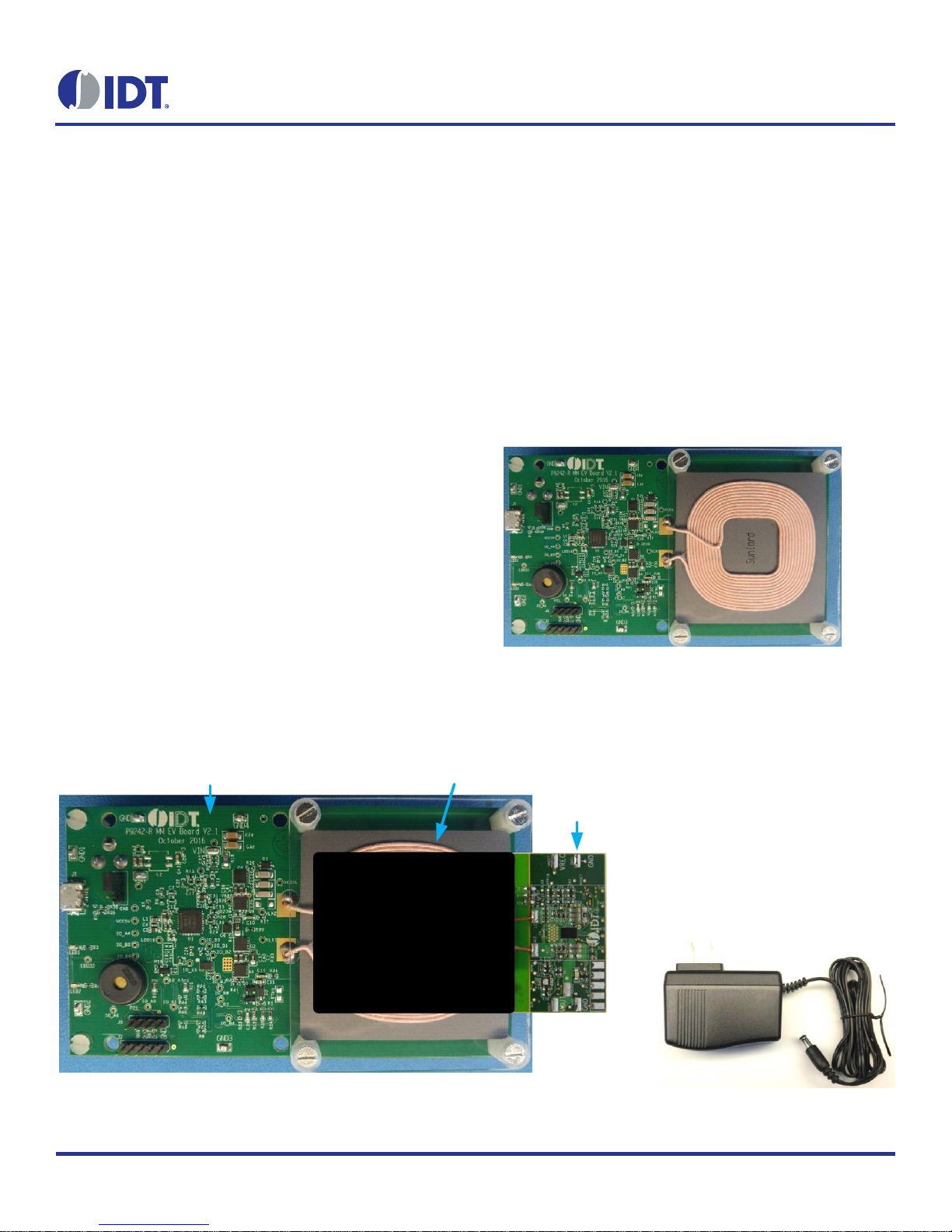
P9242-R Transmitter Evaluation Board Transmitter Coil
P9221-R-EVK
Description
The P9242-R-EVK Mass-Market Evaluation Board demonstrates
the features of the P9242-R 15W Wireless Power Transmitter
(TX). It is intended to evaluate the functionality and performance
of the P9242-R when combined with a power receiver in a
wireless charging system. The P9242-R-EVK offers the flexibility
to select parameters, such as the over-current limit threshold,
LED pattern, and external temperature sensing function. The
printed circuit board (PCB) has four layers. The P9242-R
Evaluation Board is designed to function with the P9221-R
Receiver Evaluation Board, which is ordered separately. It can
also be used with the user’s WPC-1.2.2 compliant receiver.
The high-efficiency, turnkey reference design is supported by
comprehensive online, digital resources to significantly expedite
the design-in effort and enable rapid prototyping. The total active
area is optimized to 32mm x 32mm.
Kit Contents
P9242-R-EVK Mass-Market Evaluation Board
Adaptor: 12V/2A AC
Features
P9242-R Evaluation Board with support for WPC-1.2.2
Up to 15W output power
Adjustable over-current limit
Adjustable temperature shutdown
Two programmable LED status indicators
Four-layer PCB
Total active area: 1024 mm
Fully assembled with test points and coil fixture
P9242-R-EVK Mass-Market Evaluation Board
2
P9242-R Transmitter Board Connected to P9221-R-EVK
12V/2A AC Adapter (Not to scale)
Page 2

P9242-R-EVK Evaluation Board User Manual
© 2016 Integrated Device Technology, Inc. 2 December 22, 2016
Important Notes
Disclaimer
Integrated Device Technology, Inc. and its affiliated companies (herein referred to as “IDT”) shall not be liable for any damages arising out of defects resulting
from
(i) delivered hardware or software
(ii) non-observance of instructions contained in this manual and in any other documentation provided to user, or
(iii) misuse, abuse, use under abnormal conditions, or alteration by anyone other than IDT.
TO THE EXTENT PERMITTED BY LAW, IDT HEREBY EXPRESSLY DISCLAIMS AND USER EXPRESSLY WAIVES ANY AND ALL WARRANTIES,
WHETHER EXPRESS, IMPLIED, OR STATUTORY, INCLUDING, WITHOUT LIMITATION, IMPLIED WARRANTIES OF MERCHANTABILITY AND OF
FITNESS FOR A PARTICULAR PURPOSE, STATUTORY WARRANTY OF NON-INFRINGEMENT, AND ANY OTHER WARRANTY THAT MAY ARISE BY
REASON OF USAGE OF TRADE, CUSTOM, OR COURSE OF DEALING.
Restrictions in Use
IDT’s P9242-R-EVK Mass Market Evaluation Board is designed for evaluation purposes only. It must not be used for module production or production test
setups.
Contents
1. Setup ............................................................................................................................................................................................................4
1.1 Required or Recommended User Equipment ......................................................................................................................................4
1.2 Kit Hardware Connections ...................................................................................................................................................................4
2. Usage Guide .................................................................................................................................................................................................5
2.1 Overview of the P9242-R-EVK ............................................................................................................................................................5
2.2 LED Pattern Selection .........................................................................................................................................................................6
2.3 Adjustment of Over-Current Limit ........................................................................................................................................................8
2.4 External Temperature Sensing – TS .................................................................................................................................................10
2.5 Reserved Pins ...................................................................................................................................................................................11
2.6 Transmitter Coil .................................................................................................................................................................................11
3. Schematics, Bill of Materials (BOM), and Board Layout .............................................................................................................................12
3.1 P9242-R Evaluation Board Schematics.............................................................................................................................................12
4. Bill of Materials (BOM) ................................................................................................................................................................................13
5. Board Layout ..............................................................................................................................................................................................16
6. Ordering Information ...................................................................................................................................................................................21
7. Revision History ..........................................................................................................................................................................................21
Page 3

P9242-R-EVK Evaluation Board User Manual
© 2016 Integrated Device Technology, Inc. 3 December 22, 2016
List of Figures
Figure 1. Evaluation Kit Connections using the P9221-R Receiver Evaluation Board .......................................................................................4
Figure 2. P9242-R V2.1 Evaluation Board Features...........................................................................................................................................5
Figure 3. P9242-R V2.1 Evaluation Board Details ..............................................................................................................................................5
Figure 4. R43 and R44 Schematic Location .......................................................................................................................................................7
Figure 5. R33 and R34 PCB Location ................................................................................................................................................................7
Figure 6. Over-Current Limit vs. V
Figure 7. R48 and R40 Schematic Location .......................................................................................................................................................9
Figure 8. R48 and R40 PCB Location ................................................................................................................................................................9
Figure 9. RTH1 and R20 Schematic Location ..................................................................................................................................................10
Figure 10. RTH1 and R20 R40 PCB Location ....................................................................................................................................................10
Figure 11. Silkscreen – Top of Board .................................................................................................................................................................16
Figure 12. Copper – Top Layer ...........................................................................................................................................................................17
Figure 13. Copper L1 Layer ................................................................................................................................................................................18
Figure 14. Copper L2 Layer ................................................................................................................................................................................19
Figure 15. Copper Bottom ..................................................................................................................................................................................20
.................................................................................................................................................................8
ILIM
List of Tables
Table 1. Selecting the LED Pattern ...................................................................................................................................................................6
Table 2. Recommend Coil Manufacturer .........................................................................................................................................................11
Table 3. P9242-R-EVK BOM ...........................................................................................................................................................................13
Page 4
P9242-R-EVK Evaluation Board User Manual
© 2016 Integrated Device Technology, Inc. 4 December 22, 2016
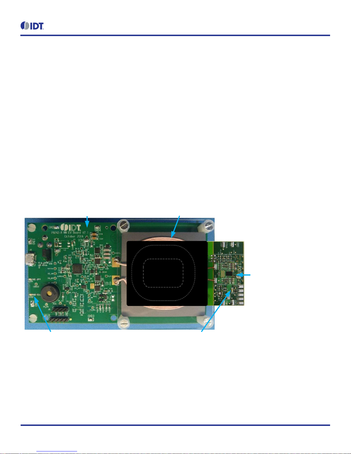
P9242-R Transmitter Evaluation Board Transmitter Coil
P9221-R-EVK
Green LEDs illuminate when connection has been established.
1. Setup
1.1 Required or Recommended User Equipment
The following additional lab equipment is required for using the kit:
P9221-R-EVK Receiver Evaluation Board or any WPC-1.2.2 compliant receiver
Power supply or 12V/2A AC adaptor
1.2 Kit Hardware Connections
Follow these procedures to set up the kit as shown in Figure 1.
1. Set up the P9242-R Evaluation Board: Plug the 12V adapter or user’s power supply into the J3 (barrel connector on the bottom of the
board) or J1 (micro USB connector).
2. Place the P9221-R-EVK or the user’s receiver on the transmitter (TX) pad with the components facing up as shown in Figure 1.
3. Verify that the two green LEDs identified in Figure 1 are illuminated indicating that coupling has been established.
4. If using the P9221-R-EVK Evaluation Board as the receiver, connect wires to the VOUT and GND test points on the P9221-R-EVK
receiver to measure the output voltage and apply a load.
Figure 1. Evaluation Kit Connections using the P9221-R Receiver Evaluation Board
Page 5

P9242-R-EVK Evaluation Board User Manual
© 2016 Integrated Device Technology, Inc. 5 December 22, 2016
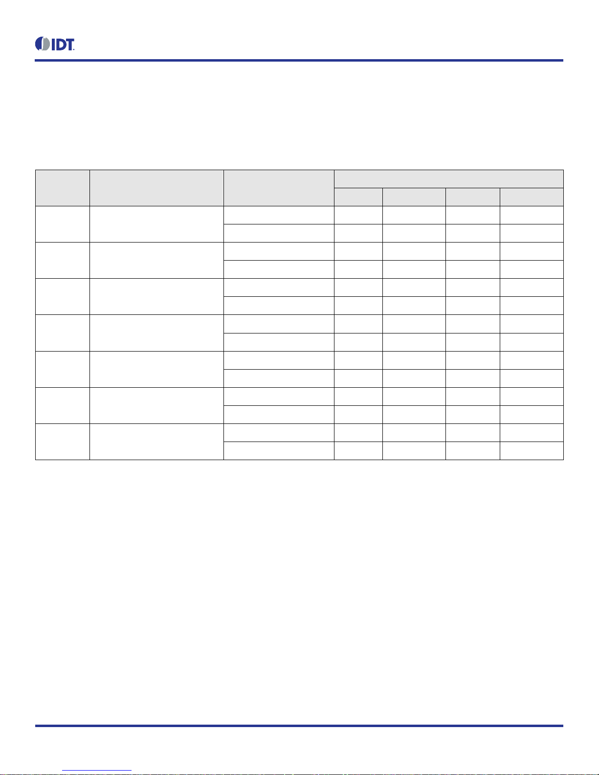
P9242-R Main IC
Buzzer
LED1 and LED2 Pattern Indicators
Vin Power Connector: Micro-USB
Vin Power Connector: Barrel Tx Coil
J2 IDT-Reserved Connector J5 IDT-Reserved Connector – Do Not Use
Unpopulated Thermistor RTH1 for
Detecting External Temperature
LED Pattern Selection
Resistors R44 and R43
VCC5V, L1, and Cout
LC Tank Capacitors
Vin Decoupling Capacitors
Tx Coil Driver External Power FETs: Q1 and Q4
Coil Current Communication
Demodulation
Iin Sense Resistor
Vin Selector
Coil Voltage Communication Demodulation
Q Measurement – FOD Detection
Tx Coil Driver External Power FETs: Q2 and Q3
LDO33 Cout
Current Limiting Resistors R40 and R48
TS Pin Threshold Selection: R20
2. Usage Guide
2.1 Overview of the P9242-R-EVK
Figure 2. P9242-R V2.1 Evaluation Board Features
Figure 3. P9242-R V2.1 Evaluation Board Details
Page 6
P9242-R-EVK Evaluation Board User Manual
© 2016 Integrated Device Technology, Inc. 6 December 22, 2016
Option
Voltage on LED_PAT Pin
LED1/LED2 Pin
Status
Standby
Transfer
Complete
Fault
1
Pull-Down or 0.075V
LED1 – GREEN
Off
On
Off
Off
LED2 – RED
Off
Off
Off
Blink 4Hz
2
0.225V
LED1 – GREEN
On
On
Off
Off
LED2 – RED
On
Off
Off
Blink 4Hz
3
0.375V
LED1 – GREEN
Off
Blink 1Hz
On
Blink 4Hz
LED2 – RED
Off
Off
Off
Off
4
0.525V
LED1 – GREEN
Off
On
Off
Blink 4Hz
LED2 – RED
Off
Off
Off
Off
5
0.675V
LED1 – GREEN
On
Blink 1Hz
On
Off
LED2 – RED
On
Off
Off
Blink 4Hz
6
0.825V
LED1 – GREEN
Off
Off
On
Off
LED2 – RED
Off
On
Off
Blink 4Hz
7
0.975V or Pull-Up
LED1 – GREEN
Off
Blink 1Hz
On
Off
LED2 – RED
Off
Off
Off
Blink 4Hz
2.2 LED Pattern Selection
The P9242-R-EVK uses two LEDs (LED1 and LED2; see Figure 2) to indicate the power transfer status, faults, and operating modes. The
LEDs are connected to the LED1 and LED2 pins as shown on P9242-R-EVK schematics (see section 3.1). The LED patterns can be selected
by setting the voltage on the LED_PAT pin through the resistor divider R43 and R44; see Table 1 for the options. On the evaluation board the
LED_PAT pin is pulled up to 3.3V through R43. R44 is unpopulated; therefore, option 7 is the default option.
Table 1. Selecting the LED Pattern
Page 7

P9242-R-EVK Evaluation Board User Manual
© 2016 Integrated Device Technology, Inc. 7 December 22, 2016
Figure 4. R43 and R44 Schematic Location
Figure 5. R33 and R34 PCB Location
Page 8

P9242-R-EVK Evaluation Board User Manual
© 2016 Integrated Device Technology, Inc. 8 December 22, 2016
0
200
400
600
800
1000
1200
1400
1600
1800
2000
2200
2400
2600
0 0.2 0.4 0.6 0.8 1 1.2 1.4 1.6 1.8 2 2.2 2.4 2.6 2.8 3 3.2 3.4
Over Current Proection[mA]
V
ILIM
[V]
2.3 Adjustment of Over-Current Limit
The over-current protection (OCP) is designed to protect the transmitter from operating conditions that could potentially cause damage or
unexpected behavior from the system. The input current is continuously monitored during the power transfer stage. If the input current goes
above the OCP threshold of the programmed current limit, the P9242-R will increase the switching frequency or reduce the duty cycle in order
to keep the input current below the OCP value. The current limit can be selected by setting the voltage on the ILIM pin through the resistor
divider R48 and R40. On the P9242-R-EVK, the ILIM pin is pulled up to 3.3V through R48. R40 is unpopulated; therefore, the current limit is
set to 2.3A.
Figure 6. Over-Current Limit vs. V
ILIM
Page 9

P9242-R-EVK Evaluation Board User Manual
© 2016 Integrated Device Technology, Inc. 9 December 22, 2016
Figure 7. R48 and R40 Schematic Location
Figure 8. R48 and R40 PCB Location
Page 10

P9242-R-EVK Evaluation Board User Manual
© 2016 Integrated Device Technology, Inc.
10
December 22, 2016
Equation 1
2.4 External Temperature Sensing – TS
The P9242-R includes an optional temperature sense input pin, TS, used to monitor a remote temperature, such as for a coil or a battery
charger.
The TS pin voltage can be calculated by Equation 1.
Where NTC is the thermistor`s resistance (RTH1) and R20 is the pull-up resistor connected to the 3.3V supply voltage on the P9242-R
Evaluation Board. The over–temperature shutdown is triggered if the voltage on the TS pin is lower than 0.6V. The RTH1 is not populated on
the P9242-R Evaluation Board.
Figure 9. RTH1 and R20 Schematic Location
Figure 10. RTH1 and R20 R40 PCB Location
Page 11

P9242-R-EVK Evaluation Board User Manual
© 2016 Integrated Device Technology, Inc.
11
December 22, 2016
Output Power
Vendor
Part Number
Inductance at 100kHz
DCR at 20°C
15W
SUNLORD
SWA53N53H30C11B
10µH
50mΩ
2.5 Reserved Pins
There are multiple reserved pins listed in the schematic: pins 13 through 16, 25 through 29, 42, and 43. These GPIOs are proprietary and for
factory use only.
2.6 Transmitter Coil
The following coil is recommended with P9242-R transmitter for 15W applications for optimum performance. The recommended vendor has
been tested and verified.
Table 2. Recommend Coil Manufacturer
Page 12

P9242-R-EVK Evaluation Board User Manual
© 2016 Integrated Device Technology, Inc.
12
December 22, 2016
Q2
DMG7430LFG
541
6
7
8
2
3
Q_DRV2
VCC_5V
LDO33
IO_B3
IO_B2
IO_B0
IO_B1
C34 0.1uF
SW_BRG2
VCOIL_OV
C33
0.1uF
R11
200K
vs3
LDO33
ISNS_IN
D1
BAV21W
VINT1
R47
5.1k
GND1
VINVIN1
R46
5.1k
IO_B1
GNDT1
R38 0
R39 0
Q8
2N7002
IO_B3
VINT2
IO_B0
IO_B2
LDO33
ILIM
LED_PAT
SCL
SDA
LDO33
OVP_CTL
C31
10uF
C30
0.1uF
GND2 GND3
GNDT2
SCL
R20 10K
LDO33
R1
1K
C29
0.1uF
GND4
J5
1122334
4
Debugg, for developmen t only
C2
0.1uF
R9 100
SLD
SLD
VCC
D-D+ID
GND
J1
usb_micro_ab
123456
789
10
11
R24
NP
LDO33
R48 10KJ4R43 10K
ISNS_H
ISNS_L
J3
AC_Adapter
LX2
LX1
R18 0.02
C17
680p
C37
10uF
C1
0.1uF
C40
10uF
VIN
R21
10
ISNS_H
C27
1uF
R15
10
Title
Size Doc ument Numb er Rev
Date: Sheet of
2.1
P9242-R MM Board V 2.1
Custom
1 1Tuesday, December 20, 2016
ISNS_L
Q_DRV1
VIN
C5
10uF
VCC_5V
VCC5V
C4
0.1uF
Q7
2N7002
R26
100K
THIS DOCUMENT CONTAINS INFORMATION PROPRIETARY
TO Integrated Device Technology, Inc. (IDT).
USE OR DISCLOSURE WITHOUT THE
WRITTEN PERMISSION OF AN OFFICER OF
IDT IS EXPRESSLY FORBIDDEN
Q6
SIA453EDJ-T1-GE3
1
2
3
4
7
5
6
8
R25
12
C22 22nF
C19
5.6nF
R13
10K
R32
100K
R7 1K
ENB
C12 1uF
C41
10uF
C3
0.1uF
C38
10uF
VBRG
R45
220
R8
100K
V_BRIDGE
L1 4.7uH
TX-Coil
assembly
R42
10K
R41
10K
C15
0.1uF
C14
10uF
R12
390K
R10
390K
R16
10K
C16
1uF
C21
0.1uF
D2
BAV21W
C35
5.6nF
R28
12
t
RTH1
R35 200K
R29
12
R5
NP
VSNS_IN
Q_DRV2
Q_DRV1
VIN
R34
100K
IO_B8
Q3
DMG7430LFG
5
4
1
6
7
8
2
3
IO_B7
C6
1uF
IO_A7
C13
0.1uF
IO_B5
LDO33
IO_B6
R27
12
LDO18
L2
NP
1
2 3
4
C42
0.1uF
C43
1uF
C10
22nF
R30
100K
R31
100K
C9
56p
R6
10K
C8
6.8nF
C7
56p
C11
22nF
D-
D+
ISNS_OUT
LDO33
GND
VCOIL
VLX1
VLX2
D-
LED_PAT
ILIM
D+
SCL
SDA
VCOIL_OV
TS
OVP_CTL
BUZR
Q1
DMG7430LFG
541
6
7
8
2
3
R23
10K
LDO33
ILIM
R40 NP
LED_PAT
R44 NP
LDO33
C32
22uF
C28
22uF
Q4
DMG7430LFG
5
4
1
6
7
8
2
3
usb_id
C36
NP
GREEN
RED
LED2
2 1
LED1
2 1
R31KR4
680
LDO33
LDO33
J2
68000-105HLF
1
1
2233445
5
C18
1nF
SDA
Programm ing Connector
C39
5.6nF
LDO18
IO_A0
IO_A1
IO_A5
IO_A6
R22 NP
GPIO
R19 NP
vs2
U2
NP
CS#1DO2WP#3GND
4
DI
5
CLK
6
HLD#
7
VCC
8
EPAD
9
PZ1
BUZZER
1
1
2
2
C44
4.7u R14
2.4K
IO_A4
C20 100nF
C23 68nF
C24 47nF
IO_B0
C25 NP
IO_B1
Q5
2N7002
IO_B2
IO_B3
IO_B4
LED1
GPIO
LED2
P9242-R
U1
EN1GND2PREG3VIN4SW_S5GND6LDO33
7
VIN_LDO8LDO189LED110LED211VDDIO
12
RSV25RSV26RSV27RSV
28
GPIO
29
GH_BRG2
30
BST_BRG2
31
SW_BRG2
32
GL_BRG2
33
GND
34
GL_BRG1
35
SW_BRG1
36
EP
49
BST_ BRG1
37
GH_BRG1
38
DRV_VIN
39
VBRG_IN
40
GND
41
42
RSV
RSV
43
VDEM1
44
IDEMI
45
ISNS_OUT
46
CSN
47
CSP
48
D-
13
D+
14
SCL
15
SDA
16
ILIM
17
LED_PAT
18
VCOIL
19
TS
20
BUZR
21
OVP_CTL
22
Q_DRV1
23
Q_DRV2
24
R33
3
R36
0.1
R37
0.1
C26
0.1uF
3. Schematics, Bill of Materials (BOM), and Board Layout
3.1 P9242-R Evaluation Board Schematics
Page 13

P9242-R-EVK Evaluation Board User Manual
© 2016 Integrated Device Technology, Inc.
13
December 22, 2016
Item
Quantity
Reference
Value
Description
Part Number
PCB Footprint
1
12
C1, C2, C3, C4, C13, C15,
C21, C26, C29, C30, C33,
C34
0.1µF
CAP CER 0.1µF 25V 10% X7R 0402
C1005X7R1E104K
050BB
0402
2 7 C5, C14, C31, C37, C38,
C40, C41
10µF
CAP CER 10µF 25V 20% X5R 0603
C1608X5R1E106M
080AC
0603 3 4
C6, C12, C16, C27
1µF
CAP CER 1µF 25V 20% X5R 0402
C1005X5R1E105M
050BC
0402 4 2
C7, C9
56pF
CAP CER 56PF 50V NP0 0402
CL05C560JB5NNN
C
0402 5 1
C8
6.8nF
CAP CER 6800PF 25V X7R 0402
GRM155R71E682K
A01D
0402 6 2
C10, C11
22nF
0.022µF 50V Ceramic Capacitor X7R 0603
GCM188R71H223K
A37D
0603 7 1
C17
680pF
CAP CER 680PF 50V X7R 0402
CL05B681KB5NNN
C
0402 8 1
C18
1nF
CAP CER 1000pF ±10% 50V X7R 0402
GRM155R71H102K
A01D
0402 9 3
C19, C35, C39
5.6nF
5600pF 100V Ceramic Capacitor C0G, NP0
0603
C1608C0G2A562J
080AC
0603
10 1 C20
100nF
CAP CER 0.1µF 100V C0G 1206
C3216C0G2A104K
160AC
1206
11 1 C22
22nF
CAP CER 0.022µF 50V 10% X7R 0402
GRM155R71H223K
A12D
0402
12 1 C23
68nF
CAP CER 0.068µF 100V NP0 1206
C3216C0G2A683K
160AC
1206
13 1 C24
47nF
CAP CER 0.047µF 100V NP0 1206
C3216C0G2A473J
115AC
1206
14 1 C25
NP
CAP CER 10000PF 100V C0G 1206
C3216C0G2A103J
115AA
1206
15 2 C28, C32
22µF
CAP CER 22µF 25V 20% X5R 1206
GRM31CR61E226
KE15L
1206
16 1 C36
NP
CAP CER 0.1µF 25V 10% X7R 0402
C1005X7R1E104K
050BB
0402
17 1 C42
0.1µF
0.10µF 50V Ceramic Capacitor X7R 0603
GRM188R71H104K
A93D
0603
18 1 C43
1uµF
1µF 25V Ceramic Capacitor X5R 0603
GRM188R61E105K
A12D
0603
19 1 C44
4.7µF
4.7µF 25V Ceramic Capacitor X5R 0603
GRM188R61E475K
E11D
0603
20 2 D1, D2
BAV21W
DIODE GEN PURP 80V 125MA DFN
BAV21W-7-F
sod123
4. Bill of Materials (BOM)
Table 3. P9242-R-EVK BOM
Page 14

P9242-R-EVK Evaluation Board User Manual
© 2016 Integrated Device Technology, Inc.
14
December 22, 2016
Item
Quantity
Reference
Value
Description
Part Number
PCB Footprint
21
30
VLX1, VINT1, IO_B1,
IO_A1, GNDT1, vs2, VLX2,
VINT2, IO_B2, GNDT2,
vs3, IO_B3, IO_B4, IO_A4,
VCC5V, IO_B5, IO_A5,
IO_B6, IO_A6, IO_B7,
IO_A7, IO_B8, LDO18,
LDO33, VSNS_IN, VCOIL,
VBRG, IO_B0, IO_A0, ENB
PTH_TP
30 GAUGE WIRE PAD
NP
TEST_PT30DPAD
22 7 VIN1, GND1, GND2,
GND3, GND4, VIN, GND
TP
TEST POINT PC MINIATURE SMT
5015
test_pt_sm_135x70
23 1 J1
5P
CONN RCPT MCR USB AB SMD TH SHLL
ZX62D-AB-5P8
usb_micro_ab
24 1 J2
68000-105HLF
BERGSTIK II .100" SR STRAIGHT
68000-105HLF
sip5
25 1 J3
AC_Adapter
CONN POWER JACK 2.5X5.5MM HI CUR
PJ-002AH
CONN_POWER_JA
CK5_5MM
26 1 J4
TP
CONN HEADER 3POS .100" STR GOLD
901200763
sip3
27 1 J5
SIP con
4 Positions Header, Unshrouded Connector
0.100" (2.54mm) Through Hole Gold or Gold,
GXT™
961104-6404-AR
sip-4
28 1 LED1
LED
LED RED CLEAR 0603 SMD
150060RS75000
0603_diode
29 1 LED2
LED
LED GREEN CLEAR 0603 SMD
150060GS75000
0603_diode
30 2 LX1, LX2
NP
Tx Coil assemble through hole
NA
TP_TXCoil
31 1 L1
4.7µH
FIXED IND 4.7µH 620MA 500 MOHM
CIG10W4R7MNC
L0603
32 1 L2
NP
Common mode EMI choke
ACM4520-901-2PT-000
EMI_TDK_ACM452
0L
33 1 PZ1
BUZZER
BUZZER PIEZO 4KHZ 12.2MM PC MNT
PS1240P02CT3
9235_buzzer
34 4 Q1, Q2, Q3, Q4
DMG7430LFG
MOSFET N-CH 30V 10.5A PWRDI3333
DMG7430LFG-7
powerdi3333_8ld_f
et
35 3 Q5, Q7, Q8
2N7002
N-Channel 60-V (D-S) MOSFET
2N7002KT1G
SOT23_3
36 1 Q6
SIA453EDJ-T1GE3
MOSFET P-CH 30V 24A PPAK SC-70-6
SIA453EDJ-T1GE3
sc70_6ld_fet
37 1 RTH1
NP
NTC Thermistor 10k Bead
NTCLE203E3103J
B0
0805
38 3 R1, R3, R7
1K
RES SMD 1K OHM 5% 1/16W 0402
RC0402JR-071KL
0402
39 1 R4
680
RES SMD 680 OHM 5% 1/16W 0402
RC0402JR07680RL
0402
40 1 R5
NP
RES SMD 0.0 OHM JUMPER 1/10W
RC0402JR-070RL
0402
41 9 R6, R13, , R16, R20, R23,
R41, R42, R43, R48
10K
RES SMD 10K OHM 1% 1/10W 0402
RC0402FR-0710KL
0402
42 5 R8, R26, R30, R31, R32
100K
RES SMD 100K OHM 5% 1/10W 0402
ERJ-2GEJ104X
0402
43 1 R24
NP
RES SMD 100K OHM 5% 1/10W 0402
ERJ-2GEJ104X
0402
44 1 R9
100
RES SMD 100 OHM 5% 1/10W 0603
RC0603JR07100RL
0603
45 2 R10, R12
390K
RES SMD 390K OHM 5% 1/10W 0603
ERJ-3GEYJ394V
0603
46 1 R14
2.4K
RES SMD 2.4K OHM 5% 1/10W 0402
ERJ-2GEJ242X
0402
47 2 R11, R35
200K
RES SMD 200K OHM 1% 1/10W 0603
RC1608F204CS
0603
48 2 R15, R21
10
RES SMD 10 OHM 1% 1/10W 0402
ERJ-2RKF10R0X
0402
Page 15

P9242-R-EVK Evaluation Board User Manual
© 2016 Integrated Device Technology, Inc.
15
December 22, 2016
Item
Quantity
Reference
Value
Description
Part Number
PCB Footprint
49 1 R18
0.02
RES SMD 0.02 OHM 1% 1/8W 0805
WSL0805R0200FE
A
0805
50 4 R19, R22, R40, R44
NP
RES SMD 10K OHM 1% 1/10W 0402
RC0402FR-0710KL
0402
51 4 R25, R27, R28, R29
12
RES SMD 12 OHM 5% 1/10W 0402
ERJ-2GEJ120X
0402
52 1 R33 3 RES SMD 3 OHM 1% 1/8W 0805
RC0805FR-073RL
0805
53 1 R34
100K
RES SMD 100K OHM 1% 1/10W 0603
ERJ-3EKF1003V
0603
54 2 R36, R37
0.1
RES SMD 0.1 OHM 5% 1/6W 0402
ERJ-2BSJR10X
0402
55 2 R38, R39
0
RES SMD 0.0 OHM JUMPER 1/10W
RC0402JR-070RL
0402
56 1 R45
220
RES SMD 220 OHM 1% 0.4W 0805
RC1206FR07220RL
1206
57 2 R46, R47
5.1k
RES SMD 5.1K OHM 5% 1/16W 0402
MCR01MRTJ512
0402
58 1 U1
P9242-R
Medium Power Transmitter
P9242-R
socketqfn_48_6x6_
0p4
59 1 U2
NP
SPIFLASH 2M-BIT 4KB UNIFORM SECT
W25X20CLUXIG
TR
uson_2x3_8LD
Page 16

P9242-R-EVK Evaluation Board User Manual
© 2016 Integrated Device Technology, Inc.
16
December 22, 2016
5. Board Layout
Figure 11. Silkscreen – Top of Board
Page 17

P9242-R-EVK Evaluation Board User Manual
© 2016 Integrated Device Technology, Inc.
17
December 22, 2016
Figure 12. Copper – Top Layer
Page 18

P9242-R-EVK Evaluation Board User Manual
© 2016 Integrated Device Technology, Inc.
18
December 22, 2016
Figure 13. Copper L1 Layer
Page 19

P9242-R-EVK Evaluation Board User Manual
© 2016 Integrated Device Technology, Inc.
19
December 22, 2016
Figure 14. Copper L2 Layer
Page 20

P9242-R-EVK Evaluation Board User Manual
© 2016 Integrated Device Technology, Inc.
20
December 22, 2016
Figure 15. Copper Bottom
Page 21

P9242-R-EVK Evaluation Board User Manual
© 2016 Integrated Device Technology, Inc.
21
December 22, 2016
Orderable Part Number
Description
P9242-R-EVK
P9242-R-EVK Evaluation Board
Revision Date
Description of Change
December 22, 2016
Initial release of document.
Corporate Headquarters
6024 Silver Creek Valley Road
San Jose, CA 95138
www.IDT.com
Sales
1-800-345-7015 or 408-284-8200
Fax: 408-284-2775
www.IDT.com/go/sales
Tech Support
www.IDT.com/go/support
DISCLAIMER Integrated Device Technology, Inc. (IDT) reserves the right to modify the products and/or specifications described herein at any time, without notice, at IDT's sole discretion. Performance
specifications and operating parameters of the described products are determined in a n independent state and are not guaranteed to perform the same way when installed in customer products. The
information contained herein is provided without representation or warranty of any kind, whether express or implied, includin g, but not limited to, the suitability of IDT's products for any particular purpose,
an implied warranty of merchantability, or non-infringement of the intellectual property rights of others. This document is presented only as a guide and does not convey any license under intell ectual
property rights of IDT or any third parties.
IDT's products are not intended for use in applications involving extreme environmental conditions or in life support systems or similar devices where the failure or malfunction of an IDT product can be
reasonably expected to significantly affect the health or safety of users. Anyone using an IDT product in such a manner does so at their own risk, absent an express, written agreement by IDT.
Integrated Device Technology, IDT and the IDT logo are trademarks or registered trademarks of IDT and its subsidiaries in the United States and other countries. Other trademarks used herein are the
property of IDT or their respective third party owners. For datasheet type definitions and a glossary of common terms, visit www.idt.com/go/glossary. All contents of this document are copyright of
Integrated Device Technology, Inc. All rights reserved.
6. Ordering Information
7. Revision History
Page 22

Mouser Electronics
Authorized Distributor
Click to View Pricing, Inventory, Delivery & Lifecycle Information:
IDT (Integrated Device Technology):
P9242-R-EVK
 Loading...