

Page 1
P9221-R-EVK Evaluation Board User Manual
© 2017 Integrated Device Technology, Inc. 1 December 18, 2017
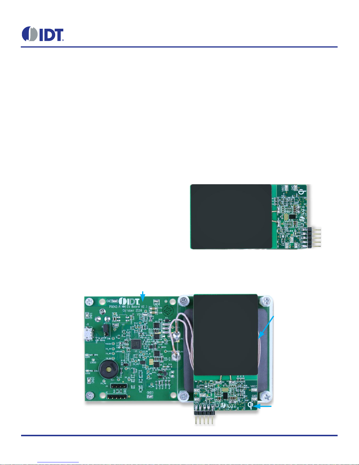
P9242-R-EVK MM Evaluation Board (Transmitter)
Transmitter Coil
P9221-R-EVK MM
Evaluation Board
(Receiver)
Description
The IDT P9221-R-EVK Mass-Market (MM) Evaluation Board demonstrates the features and performance of the P9221-R 15W
Wireless Power Receiver (Rx). The P9221-R-EVK offers the flexibility to program parameters, such as the output voltage, overcurrent limit threshold, and external temperature sensing function.
It also allows tuning the Foreign Object Detection (FOD) feature by
varying values in the resistor divider connected to the VOSET/
Q-Fact pin.
The P9221-R-EVK MM Evaluation Board is designed to function as
the receiver in a wireless power transfer system using IDT’s P9242R-EVK MM Evaluation Board as the power transmitter. The P9242R-EVK is ordered separately. The P9221-R-EVK can also be used
with the user’s WPC-1.2 compliant transmitter.
The high-efficiency, turnkey reference design is supported by
comprehensive online, digital resources to significantly expedite
design-in effort and enable rapid prototyping. The printed circuit
board (PCB) has four layers. The total active area is optimized to
28mm x 15mm.
Kit Contents
P9221-R-EVK Mass-Market Evaluation Board
Features
P9221-R-EVK MM Evaluation Board supports WPC-1.2
Up to 15W output power
Selectable output voltage: 12V or 9V
Adjustable over-current limit
External FOD tuning
Power transfer LED indicator
Alignment guide information using the PCB coils
4-layer PCB
Total active area: 420mm
2
Fully assembled with test points and coil fixture
P9221-R-EVK MM Evaluation Board
Wireless Power Transfer System using the P9221-R-EVK and P9242-R-EVK
Page 2

P9221-R-EVK Evaluation Board User Manual
© 2017 Integrated Device Technology, Inc. 2 December 18, 2017
Important Notes
Disclaimer
Integrated Device Technology, Inc. and its affiliated companies (herein referred to as “IDT”) shall not be liable for any damages arising out of defects resulting from
(i) delivered hardware or software
(ii) non-observance of instructions contained in this manual and in any other documentation provided to user, or
(iii) misuse, abuse, use under abnormal conditions, or alteration by anyone other than IDT.
TO THE EXTENT PERMITTED BY LAW, IDT HEREBY EXPRESSLY DISCLAIMS AND USER EXPRESSLY WAIVES ANY AND ALL WARRANTIES, WHETHER
EXPRESS, IMPLIED, OR STATUTORY, INCLUDING, WITHOUT LIMITATION, IMPLIED WARRANTIES OF MERCHANTABILITY AND OF FITNESS FOR A
PARTICULAR PURPOSE, STATUTORY WARRANTY OF NON-INFRINGEMENT, AND ANY OTHER WARRANTY THAT MAY ARISE BY REASON OF USAGE
OF TRADE, CUSTOM, OR COURSE OF DEALING.
Restrictions in Use
IDT’s P9221-R-EVK Mass Market Evaluation Board is designed for evaluation purposes only. It must not be used for module production or production test setups.
Contents
1. Setup ............................................................................................................................................................................................................4
1.1 Required or Recommended User Equipment ......................................................................................................................................4
1.2 Kit Hardware Connections ...................................................................................................................................................................4
2. Usage Guide .................................................................................................................................................................................................5
2.1 Overview of the P9221-R-EVK ............................................................................................................................................................5
2.2 Setting the Output Voltage and Reference Q-factor Value – VOSET/Q-Fact Pin ...............................................................................6
2.3 Alignment Aid – ALIGNX and ALIGNY ................................................................................................................................................7
2.4 Adjustment of Over-Current Limit ........................................................................................................................................................8
2.5 External Temperature Sensing and End of Charge – TS/EOC ...........................................................................................................9
2.6 Receiver Coil .....................................................................................................................................................................................10
3. P9221-R-EVK MM Evaluation Board Schematics ......................................................................................................................................11
4. Bill of Materials (BOM) ................................................................................................................................................................................12
5. Board Layout ..............................................................................................................................................................................................14
6. Ordering Information ...................................................................................................................................................................................17
7. Revision History ..........................................................................................................................................................................................17
Page 3

P9221-R-EVK Evaluation Board User Manual
© 2017 Integrated Device Technology, Inc. 3 December 18, 2017
List of Figures
Figure 1. Evaluation Kit Setup using the P9242-R-EVK MM Evaluation Board as the Transmitter ....................................................................4
Figure 2. P9221-R-EVK MM Evaluation Board V2.2 Features ...........................................................................................................................5
Figure 3. R33 and R34 Locations .......................................................................................................................................................................6
Figure 4. Recommended Structure of the X-Y Alignment Coil ............................................................................................................................7
Figure 5. R38 and R22 Location .........................................................................................................................................................................8
Figure 6. Over-Current Limit vs. ILIM Pin Voltage ..............................................................................................................................................9
Figure 7. Optional External Temperature Sensing by Connecting an RTS Thermistor ....................................................................................10
Figure 8. Silkscreen – Top of Board .................................................................................................................................................................14
Figure 9. Silkscreen – Bottom of Board ............................................................................................................................................................14
Figure 10. Top Copper Layer ..............................................................................................................................................................................15
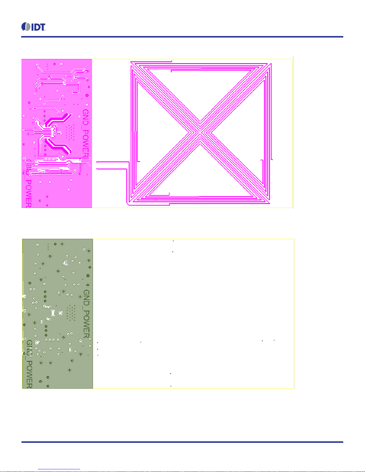
Figure 11. L2 Copper Layer ................................................................................................................................................................................15
Figure 12. L3 Copper Layer ................................................................................................................................................................................16
Figure 13. Bottom Copper Layer ........................................................................................................................................................................16
List of Tables
Table 1. Setting the Output Voltage and Reference Q-factor Value ..................................................................................................................6
Table 2. Setting the Over-Current Limit .............................................................................................................................................................8
Table 3. Recommend Coil Manufacturers .......................................................................................................................................................10
Table 4. P9221-R-EVK MM Evaluation Board BOM V2.2 ...............................................................................................................................12
Page 4
P9221-R-EVK Evaluation Board User Manual
© 2017 Integrated Device Technology, Inc. 4 December 18, 2017
1. Setup
1.1 Required or Recommended User Equipment
The following additional lab equipment is required for using the kit:
P9242-R-EVK MM Evaluation Board or any WPC-1.2 compliant transmitter
Power supply or 12V/2A AC adaptor
1.2 Kit Hardware Connections
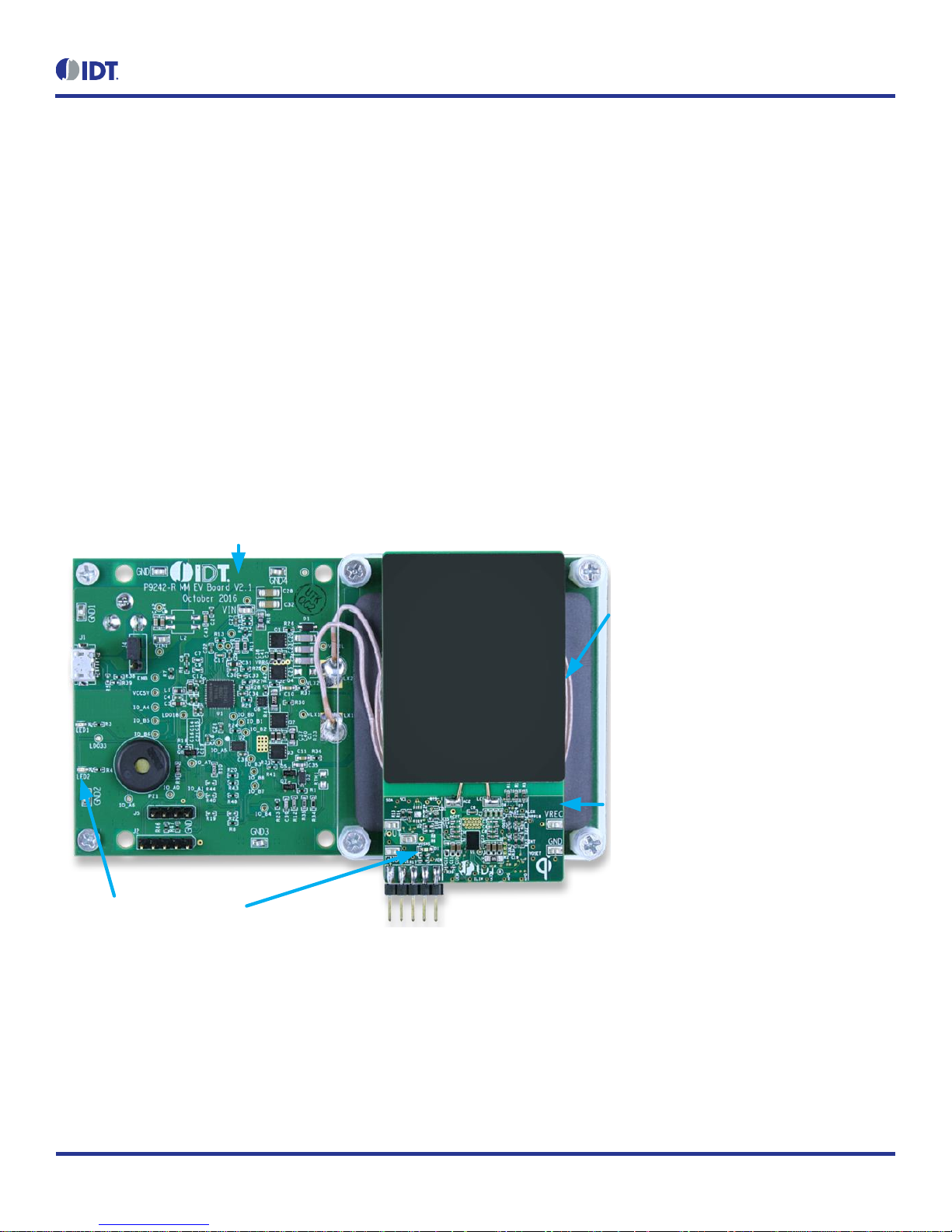
Follow these procedures to set up the kit as shown in Figure 1:
1. Set up the P9242-R-EVK Evaluation Board (or user transmitter) according to the board’s user manual.
2. Place the P9221-R-EVK on the transmitter (TX) pad with the components facing up as shown in Figure 1.
3. Verify that the green LEDs on both boards are illuminated indicating that coupling has been established.
4. Connect wires to the VOUT and GND test points to measure the output voltage and apply a load.
Figure 1. Evaluation Kit Setup using the P9242-R-EVK MM Evaluation Board as the Transmitter
P9242-R-EVK
Transmitter Coil
P9221-R-EVK
Green LEDs illuminate when
connection has been established.
Page 5
P9221-R-EVK Evaluation Board User Manual
© 2017 Integrated Device Technology, Inc. 5 December 18, 2017
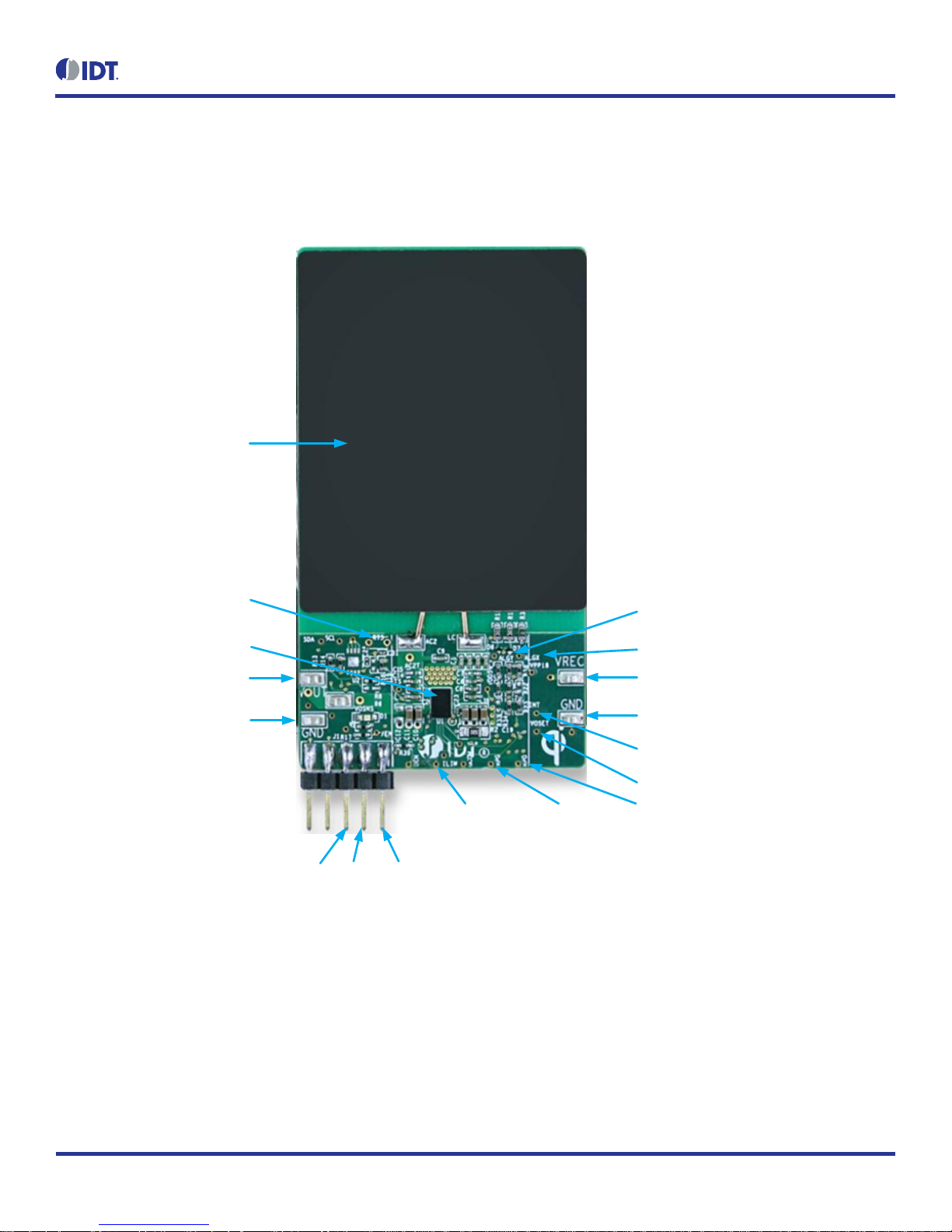
2. Usage Guide
2.1 Overview of the P9221-R-EVK
Figure 2. P9221-R-EVK MM Evaluation Board V2.2 Features
FOD Offset
Adjustment
(RPO)
External Temperature
Sensing Resistor
Output Voltage Adjustment (VOSET)
FOD Gain
Adjustment
(RPG)
Over-Current
Limit Adjustment
(ILIM)
Y- Alignment Guide Voltage (ALGY)
X- Alignment Guide Voltage (ALGX)
SCL SDA GND
GND
VRECT
GND
VOUT
Receiver Coil
IDT P9221-R IC
Interrupt Flag
Page 6
P9221-R-EVK Evaluation Board User Manual
© 2017 Integrated Device Technology, Inc. 6 December 18, 2017
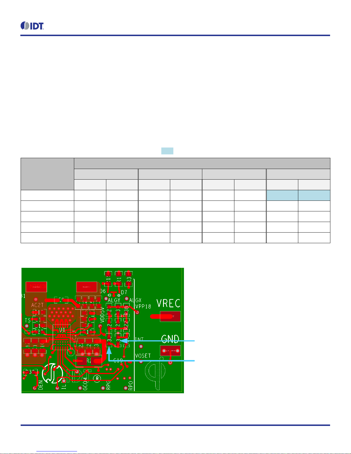
2.2 Setting the Output Voltage and Reference Q-factor Value – VOSET/Q-Fact Pin
The output voltage on the P9221-R is programmed by connecting the center tap of the divider network comprising external resistors R34 and
R33 to the VOSET/Q-Fact pin as shown in the schematic in section 3. The output voltage can be set to 9V or 12V. The recommended settings
for R33 and R34 are given in Table 1.
The default output voltage is set to 12V on the P9221-R-EVK MM Evaluation Board (R34 = 10kΩ; R33 = open). For applications where the
transmitter is capable of delivering only 5W, the P9221-R will automatically switch to 5V output to ensure 5W power delivery. The 5W option
can be disabled by changing R33 as described in Table 1. In this case, if the receiver is placed on a 5W transmitter, the receiver output pin will
be high impedance.
The VOSET/Q-Fact pin also allows setting the Q-factor value by adjusting R34 and R33 as shown in Table 1. The default value is set to 103
on the P9221-R-EVK MM Evaluation Board. For development purposes, the Q-factor should be set to 20 to avoid prematurely triggering the
Q-factor.
Table 1. Setting the Output Voltage and Reference Q-factor Value
Note: The default values on the P9221-R-EVK are indicated with blue shading.
Q Factor
Value Setting
VOUT Setting (R34/R33 Values)
9V without 5V
9V with 5V
12V without 5V
12V with 5V
R34
R33
R34
R33
R34
R33
R34
R33
103
10kΩ
4.87kΩ
Open
10kΩ
10kΩ
21kΩ
10kΩ
Open
80
10kΩ
4.32kΩ
10kΩ
0.31kΩ
10kΩ
22.6kΩ
10kΩ
324kΩ
60
10kΩ
3.65kΩ
10kΩ
0.681kΩ
10kΩ
27.4kΩ
10kΩ
147kΩ
40
10kΩ
3.09kΩ
10kΩ
1.1kΩ
10kΩ
32.4kΩ
10kΩ
90.9kΩ
20
10kΩ
2.55kΩ
10kΩ
1.54kΩ
10kΩ
39.2kΩ
10kΩ
64.9kΩ
Figure 3. R33 and R34 Locations
R34
R33
Page 7
P9221-R-EVK Evaluation Board User Manual
© 2017 Integrated Device Technology, Inc. 7 December 18, 2017
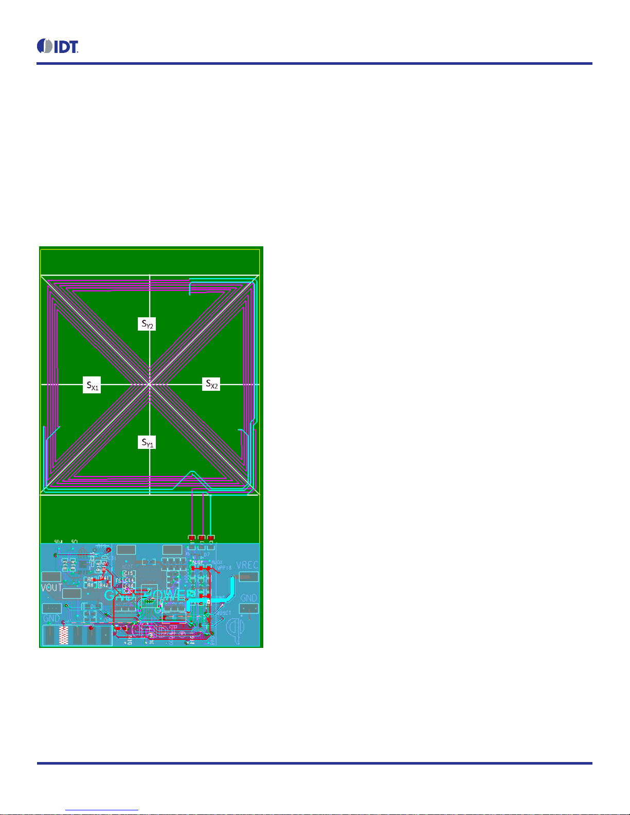
2.3 Alignment Aid – ALIGNX and ALIGNY
The signal magnitude on the P9221-R’s ALIGNX and ALIGNY pins provides directional alignment information by measuring the phase between
the input power AC signal and the horizontal (ALIGNX) and vertical (ALIGNY) alignment signals. After the signal is measured by the analog-todigital converter, the alignment information is represented by two 8-bit signed numbers, which can be read via the I2C interface from the Align_X
and Align_Y registers (see the P9221-R Datasheet).
The difference in the electromotive force (EMF) voltage of the two coils can be represented by the amount of magnetic flux, which depends on
the misalignment position of the receiver coil relative to the transmitter coil. With the combination of two symmetrical coils on the vertical (Y)
axis and horizontal (X) axis, it is possible to sense alignment in two dimensions as shown in Figure 4. The trace length and width were designed
with 452.12mm and 0.254mm respectively for each segment coil on the P9221-R-EVK MM Evaluation Board, which was assembled with the
AMOTECH ASC-504060E00-S00 coil as shown in Figure 4.
Figure 4. Recommended Structure of the X-Y Alignment Coil
Page 8
P9221-R-EVK Evaluation Board User Manual
© 2017 Integrated Device Technology, Inc. 8 December 18, 2017
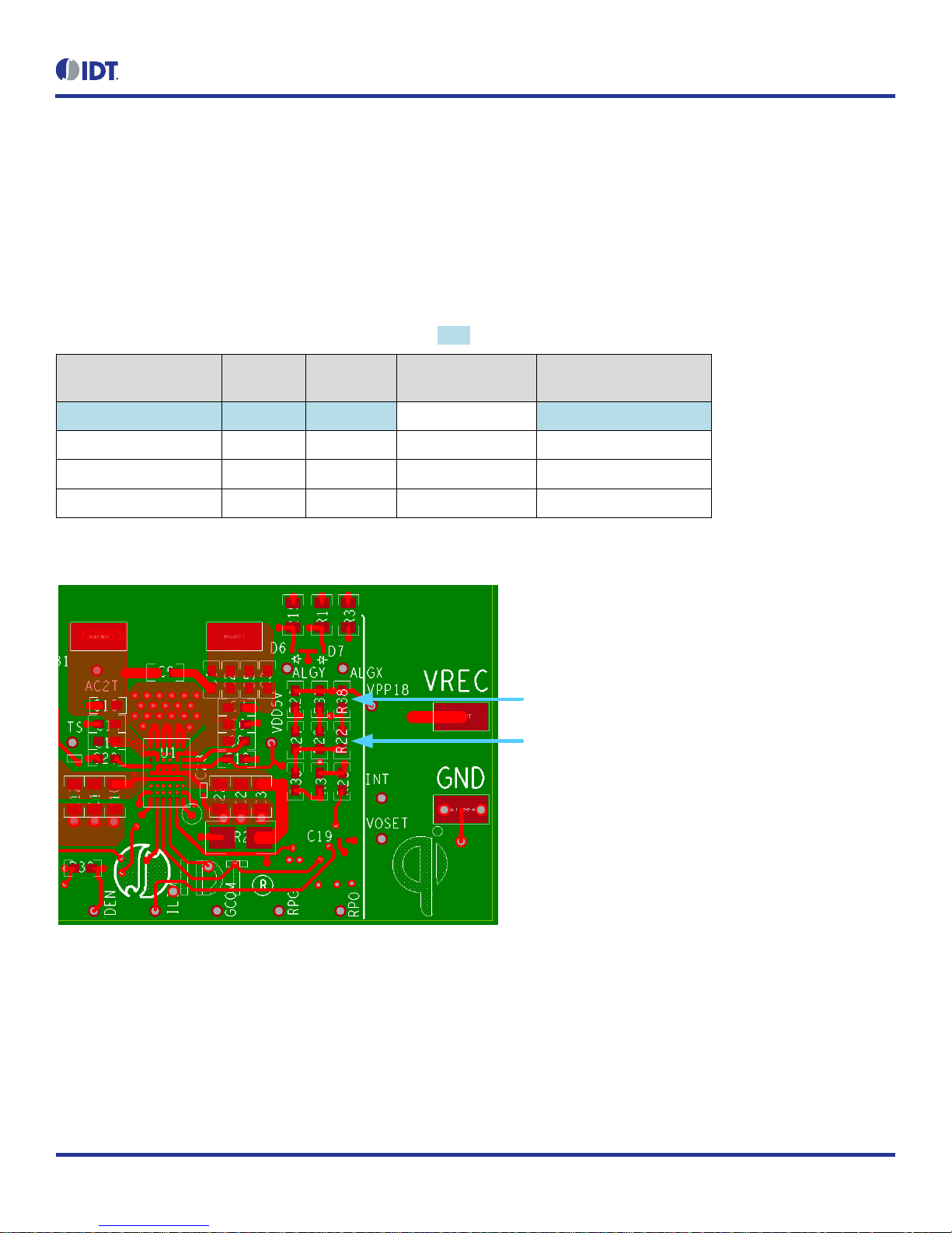
2.4 Adjustment of Over-Current Limit
The P9221-R has a programmable current limit function for protecting the device in the event of an over-current or short-circuit fault condition.
If the output current exceeds the programed threshold, the P9221-R will limit the load current by reducing the output voltage. The recommended
current limit setting is 120% of the maximum output current. The default value for the over-current limit is set to 1.6A. The ILIM pin allows
changing the over-current limit value without modification of the firmware by selecting the values of R38 and R22 as shown in Table 2. R38 and
R22 form a divider network from the 1.8V supply to ground with the center tap connected to the ILIM pin as shown in the schematic in section 3.
The voltage at the ILIM pin sets the over-current limit. See Figure 6 for the relationship between the current limit and the voltage on the ILIM
pin.
Table 2. Setting the Over-Current Limit
Note: The default values on the P9221-R-EVK are indicated with blue shading.
Voltage on ILIM Pin [V]
R38 [kΩ]
R22 [kΩ]
Maximum Output
Current [A]
Over-Current Limit [A]
Pull-up
10
Open
1.25
1.6
0.60
10
5.1
0.80 1 0.45
10
3.3
0.64
0.8
0.25
10
1.6
0.40
0.5
Figure 5. R38 and R22 Location
R38
R22
Page 9

P9221-R-EVK Evaluation Board User Manual
© 2017 Integrated Device Technology, Inc. 9 December 18, 2017
Figure 6. Over-Current Limit vs. ILIM Pin Voltage
2.5 External Temperature Sensing and End of Charge – TS/EOC
The P9221-R has a temperature sense input pin, TS, which can be used to monitor a remote temperature, such as a thermistor reading for a
coil or a battery charger. The built-in comparator’s reference voltage is 0.6V and 0.1V in the P9221-R, and it is used for monitoring the voltage
level on the TS/EOC pin as described by Equation 1.
V
TS
=
V
VDD18
∗
NTC
R19 + NTC
Equation 1
Where NTC is the thermistor`s resistance and R19 is the pull-up resistor connected to the 1.8V supply voltage on the P9221-R-EVK MM
Evaluation Board. The over–temperature shutdown is triggered when the TS pin voltage is between 0.6V and 0.1V. The RTS is not populated
on the P9221-R MM Evaluation Board.
When the TS/EOC pin is less than 0.1V, the End-of-Charge (EOC) function is activated, and the P9221-R will send the End-Power-Transfer
(EPT) packet to the transmitter terminating the power delivery.
0
200
400
600
800
1000
1200
1400
1600
0 0.1 0.2 0.3 0.4 0.5 0.6 0.7 0.8 0.9 1
ILIM [mA]
V
ILIM
[V]
Page 10

P9221-R-EVK Evaluation Board User Manual
© 2017 Integrated Device Technology, Inc.
10
December 18, 2017
Figure 7. Optional External Temperature Sensing by Connecting an RTS Thermistor
RTS
2.6 Receiver Coil
The ASC-504060E00-S00 coil is used in the kit. The following alternative coils are recommended for the P9221-R receiver for 15W applications
for optimum performance. The recommended vendor coils have been tested and verified as shown in Table 3.
Table 3. Recommend Coil Manufacturers
Output Power
Vendor
Part Number
Inductance at 100kHz
ACR at 20°C
Series Resonant Capacitance
15W
AMOTECH
ASC-504060E00-S00
8.2µH
220mΩ
400nF
15W
TDK
WR424245-13K2-G
11.2µH
170mΩ
300nF
15W
SUNLORD
SWA50R40H06C02B
8.4µH
150mΩ
400nF
15W
WURTH
760308102207
8.0µH
80mΩ
400nF
Page 11

P9221-R-EVK Evaluation Board User Manual
© 2017 Integrated Device Technology, Inc.
11
December 18, 2017
3. P9221-R-EVK MM Evaluation Board Schematics
D1
LED
C12
NP
C10
10uF
INT
INT
SDA
C9
3.3nF
R18
NP
VDD5V
D6
5.1V
R8 0
RSV1
C25
NP
ALGX
R33
NP
R39
10k
C19
0.1uF
C21
10uF
C16
15nF
U1
P9221-R
COMM1
A1
COMM2
A6
RSV4
B1
RSV5
B6
EN
B5
ALIGNX
A2
SCL
A3
VOSET/Q-Fact
A4
RPPG
A5
SDA
B3
ALIGNY
B2
ILIM
B4
RPPO
C4
DEN
C5
OUT
D1
INT
C3
SINK
C2
OUT1D2OUT2
D3
OUT3D4OUT4
D5
OUT5
D6
VRECTE1VRECT1
E2
VRECT2E5VRECT3
E6
VRECT4F2VRECT5
F3
VRECT6F4VRECT7
F5
AC1G2AC1_1
H1
AC1_2
H2
AC2G5AC2_1
H5
AC2_2
H6
BST1
G1
BST2
G6
PGND
C1
PGND1
C6
PGND2
J1
PGND3
J2
PGND4
J3
PGND5
J4
PGND6
J5
PGND7
J6
VDD5V
F1
VDD18
F6
RSV3
G3
RSV2
H3
RSV1
G4
TS/EOC
H4
C20
1uF
/EN
R19
10K
I2CRAI L
VOUT
VOSET
P9221-R MM EV Board V2.2
C31
0.1uF
C8
15nF
VRECT
R35 0
J1
I2C
1
2
3
4
5
L1
SCL
R28
NP
R17 10k
VPP18
R42
NP
VDD5V
R22
NP
R2
36
R14
5.1k
C3
100nF/50V
RPO
C11
10uF
RSV1
R13
5.1k
TS
VOUT
C23
0.1uF
GND1
R16 10K
VRECT
R29
10K
C7
NP
VOSNS
ILIM R34
10k
R23
10k
C22
10uF
VDD5V
R38
10K
RX Power Coil
AlignX coil
C18
1uF
C6
47nF
VPP18
Vrect
R1
5.1k
ALGY
TS
C2
100nF/50V
D7
5.1V
U2
NP
A0
1
A1
2
A2
3
VSS
4
SDA
5
SCL
6
WP
7
VCC
8
E_PAD
9
VPP18
RTS
NP
VPP18
C1
100nF/50V
AlignY coil
WP
C5
100nF/50V
R41
NP
LC
SDA
INT
R27
10K
VOUT
C33
10uF
DEN
R30
NP
AC2T
TS
C15
NP GND
SCL
R6 NP
R15 10K
GCOM
AC2
RPG
C14
47nF
Page 12
P9221-R-EVK Evaluation Board User Manual
© 2017 Integrated Device Technology, Inc.
12
December 18, 2017
4. Bill of Materials (BOM)
Table 4. P9221-R-EVK MM Evaluation Board BOM V2.2
Item
Reference
Quantity
Value
Description
Part number
PCB Footprint
1
AC2T, VDD5V,
VPP18, VOSET, TS,
SDA, SCL, RPO,
RPG, INT, ILIM,
GCOM, DEN, ALGY,
ALGX, /EN
16
PTH_TP
Test Pad
10MIL_35PAD
2
AC2, LC
2
NP
TEST POINT
test_pt_sm_135x70
3
C1, C2, C3, C5
4
100nF
CAP CER 0.1µF 50V X5R 0402
GRM155R61H104KE19D
0402
4
C6, C14
2
47nF
CAP CER 0.047µF 50V X7R 0402
C1005X7R1H473K050BB
0402
5
C7, C15
2
NP
CAP CER 0.047µF 50V X7R 0402
C1005X7R1H473K050BB
0402
6
C8, C16
2
15nF
CAP CER 0.015µF 50V X7R 0402
GRM155R71H153KA12J
0402
7
C9 1 3.3nF
CAP CER 3300PF 50V X7R 0402
CL05B332KB5NNNC
0402
8
C10, C11, C21, C22,
C33
5
10µF
CAP CER 10µF 25V X5R 0603
CL10A106MA8NRNC
0603
9
C12 1 NP
CAP CER 10µF 25V X5R 0603
CL10A106MA8NRNC
0603
10
C18,C20
2
1µF
CAP CER 1µF 10V X5R 0402
GRM155R61A105KE15D
0402
11
C19,C31
2
0.1µF
CAP CER 0.1µF 10V X5R 0201
C0603X5R1A104K030BC
0201
12
C23 1 0.1µF
CAP CER 0.1µF 25V X5R 0201
CL03A104KA3NNNC
0201
13
C25 1 NP
CAP CER 0.1µF 10V X5R 0201
C0603X5R1A104K030BC
0201
14
D1 1 LED
LED GREEN CLEAR 0603 SMD
150 060 GS7 500 0
0603_diode
15
D6,D7 2 5.1V
DIODE ZENER 5.1V 100MW 0201
CZRZ5V1B-HF
0201
16
GND1, VRECT,
VOUT, VOSNS,
GND
5
Test
Point
TEST POINT PC MINIATURE SMT
5015
test_pt_sm_135x70
17
J1 1 I2C
HEADER_1X5_0P1PITCH60P42D
68002-205HLF
header_1x5_0p1Pit
ch60p42d
18
L1 1 8.2µH
Wireless power receiver coil
ASC-504060E00-S00
sm_135x70
19
RTS 1 NP
NTC2
20
R1, R13, R14
3
5.1kΩ
RES SMD 5.1K OHM 5% 1/16W
0402
MCR01MRTJ512
0402
21
R2 1 36Ω
RES SMD 36 OHM 5% 1/2W 0805
ERJ-P06J360V
0805
22
R6 1 NP
RES SMD 0.0OHM JUMPER
ERJ-2GE0R00X
0402
23
R8 1 0Ω
RES SMD 0.0OHM JUMPER 1/10W
0402
ERJ-2GE0R00X
0402
24
R15, R16
2
10KΩ
RES SMD 10K OHM 1% 1/10W
0603
RC0603FR-0710KL
0603
Page 13

P9221-R-EVK Evaluation Board User Manual
© 2017 Integrated Device Technology, Inc.
13
December 18, 2017
Item
Reference
Quantity
Value
Description
Part number
PCB Footprint
25
R17, R19, R23, R27,
R29, R34, R38, R39
8
10kΩ
RES SMD 10K OHM 5% 1/16W
0402
CRCW040210K0JNEDIF
0402
26
R18, R22, R28, R30,
R33, R41, R42
7
NP
RES SMD 10K OHM 5% 1/16W
0402
CRCW040210K0JNEDIF
0402
27
R35 1 0Ω
RES SMD 0.0OHM 1/10W 0603
MCR03EZPJ000
0603
28
U1 1 P9221-R
MP Wireless power receiver
P9221-R
csp52_2p64x3p94_
0p4mm
29
U2 1 NP
IC EEPROM 128KBIT 400KHZ
8TDFN
24AA128T-I/MNY
TDFN08
Page 14
P9221-R-EVK Evaluation Board User Manual
© 2017 Integrated Device Technology, Inc.
14
December 18, 2017
5. Board Layout
Figure 8. Silkscreen – Top of Board
Figure 9. Silkscreen – Bottom of Board
Page 15

P9221-R-EVK Evaluation Board User Manual
© 2017 Integrated Device Technology, Inc.
15
December 18, 2017
Figure 10. Top Copper Layer
Figure 11. L2 Copper Layer
Page 16
P9221-R-EVK Evaluation Board User Manual
© 2017 Integrated Device Technology, Inc.
16
December 18, 2017
Figure 12. L3 Copper Layer
Figure 13. Bottom Copper Layer
Page 17

P9221-R-EVK Evaluation Board User Manual
© 2017 Integrated Device Technology, Inc.
17
December 18, 2017
6. Ordering Information
Orderable Part Number
Description
P9221-R-EVK
P9221-R-EVK MM Evaluation Board
7. Revision History
Revision Date
Description of Change
December 18, 2017
Updates for V2.2 of the P9221-R-EVK.
Minor edits.
December 19, 2016
Initial release of document.
Corporate Headquarters
6024 Silver Creek Valley Road
San Jose, CA 95138
www.IDT.com
Sales
1-800-345-7015 or 408-284-8200
Fax: 408-284-2775
www.IDT.com/go/sales
Tech Support
www.IDT.com/go/support
DISCLAIMER Integrated Device Technology, Inc. (IDT) and its affiliated companies (herein referred to as “IDT”) reserve the right to modify the products and/or specifications described herein at any time,
without notice, at IDT's sole discretion. Performance specifications and operating parameters of the described products are d etermined in an independent state and are not guaranteed to perform the same
way when installed in customer products. The information contained herein is provided without representation or warranty of a ny kind, whether express or implied, including, but not limited to, the suitability
of IDT's products for any particular purpose, an implied warranty of merchantability, or non -infringement of the intellectual property rights of others. This document is presented only as a guide and does not
convey any license under intellectual property r ights of IDT or any third parties.
IDT's products are not intended for use in applications involving extreme environmental conditions or in life support systems or similar devices where the failure or malfunction of an IDT product can be
reasonably expected to significantly affect the health or safety of users. Anyone using an IDT product in such a manner does so at their own risk, absent an express, written agreement by IDT.
Integrated Device Technology, IDT and the IDT logo are trademarks or registered trademarks of IDT and its subsidiaries in the United States and other countries. Other trademarks used herein are the
property of IDT or their respective third party owners. For datasheet type definitions and a glossary of common terms, visit www.idt.com/go/glossary. All contents of this document are copyright of Integrated
Device Technology, Inc. All rights reserved.
 Loading...