

IDT Microclock 5X1503L, Microclock 5X1503, Microclock 5L1503L, Microclock 5L1503S, Microclock 5X1503S User Manual
...Page 1
Microclock® 5X1503/5L1503 Family Development Kit
User Guide
Introduction
The Microclock development kit is designed to support the 5X1503/5L1503 devices. It provides a convenient way of verifying, configuring
and programming the blank parts for Microclock devices 5X1503 and 5L1503. The IDT Timing Commander
for configuration and frequency validation on a socket board through a USB programmer board in USB interface. The development kit
support programming to Microclock blank parts either placed into a socket of the board or the blank device soldered on evaluation boards
as additional extension boards.
Table 1. 5X1503/5L1503 Family of Products
Product Description Package
5X1503 1.8V integrated with an internal 52MHz crystal (standard 5X1503). 10-DFN
5L1503 1.8V using an external crystal (standard 5L1503). 10-DFN
5X1503L 1.8V integrated with an internal 52MHz crystal, low output swing at channel 1. 10-DFN
5L1503L 1.8V using an external crystal, low output swing at channel 1. 10-DFN
5X1503S 1.8V integrated with an internal 52MHz crystal. (support spread spectrum clock). 10-DFN
™ GUI supports to the devices
5L1503S 1.8V using an external crystal. (support Spread spectrum clock). 10-DFN
Limit of VCO for Each Microclock Device
▪ For standard 5X1503 / standard 5L1503:
• F
: 50MHz – 130MHz
VCO
▪ For 5X1503L / 5L1503L:
• F
: 50MHz – 130MHz
VCO
▪ For 5X1503S / 5L1503S:
• F
: 500MHz – 1100MHz
VCO
Socket Board Overview
The Microclock socket board builds in with a Microclock evaluation part (standard 5X1503 product) with all of the necessary components
and connections to test the functionality of the configuration. Users can use the evaluation part for configuration. Once the configuration
is final, users can either place blank parts in the socket or connect to a separated evaluation board with a soldered blank part for
programming.
Use Figure 1 and Table 2 to identify board items and features.
1©2019 Integrated Device Technology, Inc. July 8, 2019
Page 2

Microclock® 5X1503/5L1503 Family Development Kit User Guide
10
1
2
12
11
5
4
3
6
7
8
9
Figure 1. Socket Board Overview (5X1503 board shown in below with socket closed)
Table 2. Socket Board Descriptions
Label Number Label Name Description
10
11 DIP Switch
12 Socket 10-DFN socket for placing Microclock blank parts.
1 Device ID (5x1503) The evaluation board name supports 5X2503 or 5L2503.
2 Connectors Two set of connectors support configuration programming on evaluation board.
3Jumper
4 Test Points Test points for Output 1, Output 2, and Output 3 from evaluation part.
5 LEDs Two LED lights to indicate the OTP burn process.
6 External crystal The footprint of external crystal supports 5L1503 / 5L1503L / 5L1503S.
7 SMA Connector Connector for supporting either input of external clock for CLKINB/X2 pin or PPS Mode on SE1.
8 SMA Connector Connector for supporting either input of external clock for CLKIN/X1 pin or PPS Mode on OE1.
9 Part Indication Indication for device orientation.
Switch Control on OE1
and OE2
A switch jumper to control OTP programming function to blank parts either in the socket or
evaluation board through the connector.
Two switch controls to enable/disable outputs in hardware mode from DIP switch.
Used to configure the device in different modes (software mode as default for I2C control;
hardware mode as output pin control selection).
2©2019 Integrated Device Technology, Inc. July 8, 2019
Page 3
Microclock® 5X1503/5L1503 Family Development Kit User Guide
1
6
54
3
2
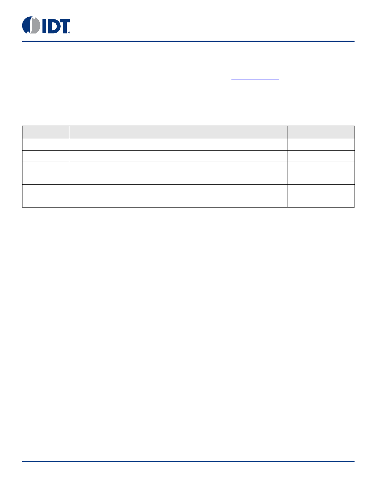
Figure 2. Evalua tion Board Overview (5X1503 evaluation board shown in below)
Table 3. Evaluation Board Desc ri ptions
Label Number Label Name Function
1 Test Points Test points for PIN6, PIN7, PIN8, PIN9, and PIN10 (in order of appearance from left to right).
2 5X1503 Microclock device soldered on evaluation board.
3 External Crystal The footprint of external crystal supports for 5L1503 / 5L1503L / 5L1503S.
4 Test Points Test points for PIN5, PIN4, PIN3, PIN2, and PIN1 (in order of appearance from left to right).
5 Part Indication Indication for device orientation.
6 Headers for Connector Separated for 2 and 4 headers as connection between socket and evaluation boards.
3©2019 Integrated Device Technology, Inc. July 8, 2019
Page 4
Microclock® 5X1503/5L1503 Family Development Kit User Guide
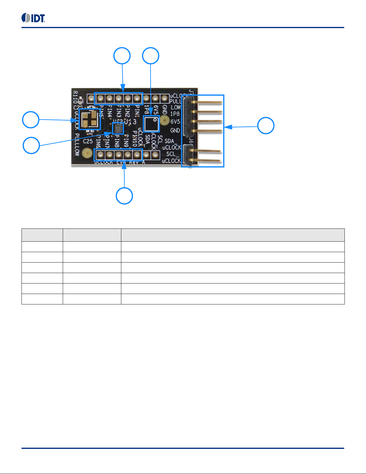
Socket Board
USB Programmer Board
Evaluation Board
Pin 1 Orientation
Pin 1 Orientation
Ground Pin
Ground Pin
VDD 1.8V Pin
OTP Burn Pin
SDATA Pin
SCLK Pin
Figure 3. Development Kit Boards
The socket board for all Microclock products, combined with a USB programmer board, is used for the purpose of validation and
measurement on all outputs. The development kit offers two ways to program a configuration to either a blank part in the socket or a
blank part soldered on an evaluation board for validation. Blank parts can drop into the socket of the socket board for programming on
different MicroClock family devices. The evaluation board is another option for configuration programming so it can be brought over to
any system board for clocking support. Note that blank parts can only be burnt once through the socket board. The socket board is
bundled with a USB programmer board. The following description and images are restricted to the socket board.
On the footprint of the socket board, a pin orientation identifies the position of Pin 1 as shown in Figure 4. Align the dot of the blank part in
the socket as pointed. After placing the blank part, secure the socket cover.
Figure 4. Socket Board (pin position)
Figure 5. Evaluation Board (pin position)
4©2019 Integrated Device Technology, Inc. July 8, 2019
Page 5

Microclock® 5X1503/5L1503 Family Development Kit User Guide
Programming Steps
Use programming steps 2 – 7 as described in the Table 4 to program a configuration into the blank part in the specified socket board.
.
Table 4. Programming Steps
Step Number Step description Comments
0
A configuration has been validated and
completed on the development kit.
All intended outputs should be available
1
for
measurement on the USB
development kit.
Plug the specified socket board onto
2
the USB programmer board (shown in
Figure 3).
Start Timing Commander software (this
3
step can be skipped if a configuration is
ready in the personality).
New settings file (this step can be
4
skipped if a configuration is ready in the
personality).
5 Connect to the development kit.
Configurations should have programmed to the 12-pin evaluation part for validation
on the socket board through the USB programmer board using Timing Commander.
Upon validation of the outputs, “Disconnect” the USB board and proceed for OTP burn
as explained in the following sections.
USB programmer board with the socket board provides a communication channel
between the GUI and a blank part in the socket board.
Launch the Timing Commander GUI software. Load the personality file.
Using the Timing Commander GUI, start a new settings file or open a pre-optimized
file.
Click on the chip symbol on the top right corner of the GUI window.
Once connected, new options will be available on a green background indicating that
the USB programmer board has successfully connected with the socket board.
6—
The configuration will be programmed into the blank part in the socket.
7 Click the “Write all” icon.
5©2019 Integrated Device Technology, Inc. July 8, 2019
Page 6

Microclock® 5X1503/5L1503 Family Development Kit User Guide
Use the following steps to proceed with the OTP burn.
8. After the chip is connected to the Timing Commander, the main window of configuration is shown (see Figure 6). Click the OTP icon
on the left side of personality window.
Figure 6. Personality Main Window
9. After clicking the icon, a new dialogue window will open (see Figure 7). Set the burning protection for the desired Config/DFC to
configure the OTP Burn (default is “Burn”). Click “Burn” to proceed with the OTP burn process. Please note that this process cannot
be reverted back.
Figure 7. Burn Dialog Window
6©2019 Integrated Device Technology, Inc. July 8, 2019
Page 7

Microclock® 5X1503/5L1503 Family Development Kit User Guide
10. Once “Burn” is clicked, a dialog of confirmation will appear verifying if the development kit has connected with user PC for OTP
programming. Click “Yes” to proceed with the OTP burn.
Figure 8. Connection Confirmation Window
11. If the OTP burn process is successful, a dialog window with “Success” will appear indicating that the process is completed and the part
has been burnt based on the configuration.
Figure 9. Success Dialog Window
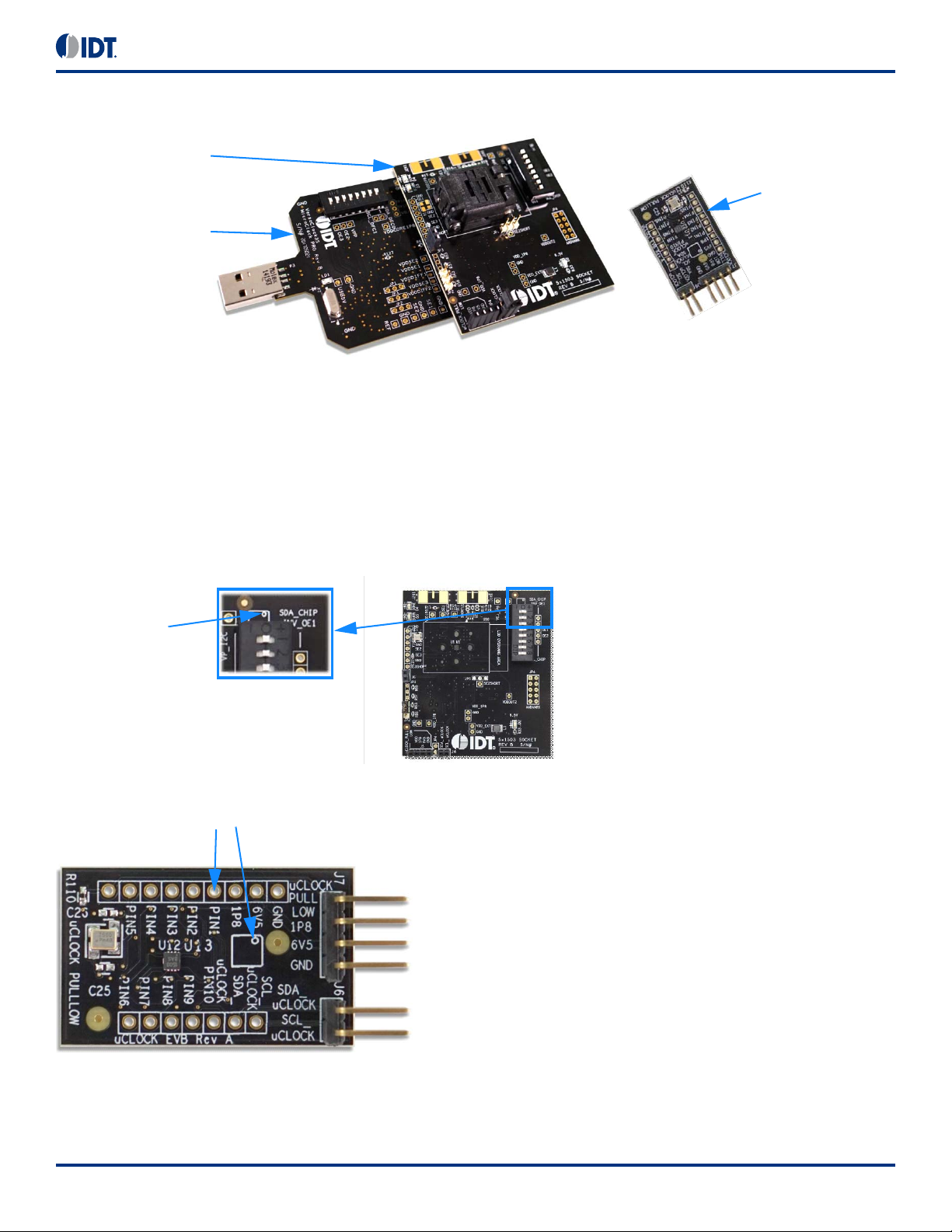
JP2 on MicroClock socket board provides a select function for configuration programming to either the evaluation part or blank parts in
socket or on an evaluation board. To program OTP on a blank part in the socket or an evaluation board, ensure to un-plug the jumper on
JP2 (default jumper sets to be plugged). See Figure 10.
Figure 10. Jumper Setup
Figure 11. Connection between Socket Board and Evaluation Board
7©2019 Integrated Device Technology, Inc. July 8, 2019
Page 8

Termination Options–Default
Table 5. Termination for Single-end ed Output (option 1)
Signal Type Series Resistor, R4
LVCMOS for VDDO set at 1.8V 22Ω
LVCMOS for VDDO set at 1V, 1.1V and 1.2V 20Ω
LVCMOS for 32.768kHz output 0 Ω
Table 6. Termination for Single-end ed Output (option 2)
Signal Type Series Resistor, R2
LVCMOS for VDDO set at 1.8V 22Ω
LVCMOS for VDDO set at 1V, 1.1V and 1.2V 20Ω
Table 7. Termination for Single-end ed Output (option 3)
Microclock® 5X1503/5L1503 Family Development Kit User Guide
Signal Type Series Resistor, R1
LVCMOS 22Ω
LVCMOS for VDDO set at 1V, 1.1V and 1.2V 20Ω
Schematics
Development kit socket board and evaluation board schematics are shown on the following pages.
8©2019 Integrated Device Technology, Inc. July 8, 2019
Page 9

LT1317B
U4
VIN
6
SHDN#
3
VC1GND
4
SW
5
LBI
7
FB
2
LBO
8
TP23
J1
TE_AMP_4-175638-0
1
1
2
2
3
3
4
4
556
6
7
7
8
8
9
9
10
10
R9 0_NP
12
R410
1 2
SDA_Tiny
R3 0_NP
1 2
C_01
VDD_1p8
SDA_AADVAR
C30.1 uF _NP
12
C_02
R34
20K
12
R120_NP
12
VDD_1p8
TP17
TP
1
VDD_1p8
C_03
JP3
Header_3Pin
TP20
R39 0
1 2
OE_R1
R4710K
12
C_07
TP1
SE1Short_TP
1
CLKINB/X2
R60
0
1 2
R67
22
1 2
TP24
Gate (Pin1)
Note#4
R112
0_NP
1 2
R740
12
FEMALE connector
R4810K
12
R52
10K
12
R40N P_0
1 2
Socket_GND_trace
C_03
GND for SE
outputs
VDD_1p8
GND for SE
outputs
LED_Burn
TP_SE1
R71
22
1 2
GND
TP_SE2
JP4
CON2
1
1
2
2
CLKIN/X1
C_02
R31
10K
12
C_07
R79 100
1 2
R42 NP_0
1 2
U7
MOS-P
1
2 3
TP21
6V5
U5
LTC4312
DISCEN
1
VCC
2
SCLO#1
3
SDAO#1
4
SDAIN
5
SCLIN
6
SCLO#2
7
SDAO#28EN2
9
EN1
10
FAULT#
11
VCC2
12
NC13
13
NC14
14
GND
15
ACC#
16
TP14
GND
1
VDD_SEx
LED_DONE
R18
33_NP
1 2
CLKIN/X1
R82 10K
1 2
C_04
C29
30pF_NP
12
R46 10K
12
CLKIN/X1
U1
5L1503
OE1
1
SE1
2
VDD
3
X2
4
X15VSS
6
OUT3
7
VDDO
8
OE2
9
OUT2
10
J2
TE_AMP_4-175638- 0
1
1
2
2
3
3
4
4
556
6
7
7
8
8
9
9
10
10
VDD_SEx
R78 100
1 2
This device is
placed as a symbol
for for socket
R55
0_NP
1 2
R83 NP_10K
1 2
R14
0_NP
1 2
R56
10K
12
R5 22_N P
1 2
U10
5X1513
SCL
1
SDA
2
OE1
3
OUT1
4
VDD5VSS
6
OUT3
7
VDDO
8
OE2
9
OUT2
10
R87
0_NP
R66
10k
12
Drain (Pin3)
R63
10K
12
C_09
TP5 VDD 1P8
1
Node#2
VDD33
JP6
Header_3Pin_NP
R54
NP_10K
12
SSM3J338R
OE2
SDA_DFC 0
VDD33
USB P1 connector
VDD_USB1p8_ J7
Node#4
6v5_en
R64
0_NP
1 2
R59
2.2
1 2
OE1
C161 uF
12
JP2
Header_3Pin_NP
R7
0_NP
1 2
TP11
SE1_TP
1
Tiny_pull_low
R57
NP_10K
12
VDD33
TP8
VDD_Ext_TP
1
Pls make sure they match to the
location of connectors from USB
board
C_04
6v5_en
REG_COMP1
TP_SE3
SW5
R2
0_NP
1 2
REG_COMP
SCL_DFC_socket
FEMALE connector
C_01
J5
CON4
1
1
2
2
3
3
4
4
C_09
SCL_chip
R19
200K_NP
12
No populated
unless for PPS
VDD33
J1X1
R44
10K
12
C_01
R73
10k
12
VDD_SExVDD_USB1p 8_J6
R111
10K
1 2
U2
TC7SZ125FE
2 4
5
1
FB1
BLM18AG601SN1D
1 2
VDD_1p8_BF-F ET
C17
0.1 uF_NP
12
LED_Burn
GNDGND
Y1
25 MHz 8 pF_NP
4
1
2
3
BURN
INV_OE1
CLKIN/X1
Source (Pin2)
Node#5
R32
237K_1%
12
VDD_1p8
6V5
R50
NP_10K
12
VDD33
VDD_SEx
D3
LED_RED
12
J2X1
R80 10K
1 2
GND
VDD_SEx
SDATA_DFC
VDD33
R81 10K
1 2
TP41 VDD 1P8
1
VDD33
VDD33
C60.1 uF
12
R15
0_NP
1 2
TP18
VP_I2C
1
C9 .01uF
12
R6
10K_NP
1 2
SDA_Tiny
R21
0_NP
1 2
JP5
Header_10P in_NP
1
3
5
7
9
2
4
6
8
10
R37
0
1 2
C1130pF_NP
12
C1510 uF
12
C1NP_ 8pf
12
R49 10K
12
SW2
SW4
C_09
TP15
GND
1
C4
10 uF
12
LED_Burn
C_07
SCLK_Tiny
U6
SN74LVC1G04DBV
NC
1
A
2
GND3Y
4
VCC
5
VDD_SEx_ BF-FET
Source (Pin2)
6V5
CLKINB/X2
Pin10_Vddout2
Silkscreen
as VPP
GND for SE
outputs
C212pF
12
C50. 1 uF
12
SDATA_DFC
FEMALE connector
C_10
VDD_1p8
R43
10K
12
OE2
TP3
SE1Short_TP
1
D4
LED_GREEN
12
X2
SW3
OE1
SCLK_M
R77
10K_NP
12
J3
TE_AMP_4-175638-0
1
1
2
2
3
3
4
4
556
6
7
7
8
8
9
9
10
10
Tiny_pull_low
U3
5X1503
SCL
1
SDA
2
OE1
3
OUT1
4
VDD5VSS
6
OUT3
7
VDDO
8
OE2
9
OUT2
10
TP_SE1
C_05
R30
1M_1%
1 2
Gate (Pin1)
LED_DONE
1 inch traceline on
SE1, SE2 and, SE3
SCLK_Tiny
SDA_Tiny
U9
MOS-P
1
2 3
VDD_SEx
TP2
SE2Short_TP
1
R62
0
1 2
R51
10K
12
C13 .01uF
12
VDD_1p8
Inverse_Tiny
C_05
R36
0
1 2
R13
0_NP
1 2
C8
1500pF
12
C_03
R4
0_NP
1 2
D2
LED
12
R58
0
1 2
SDA_DFC 0
R70
2.2
1 2
VDD_Ext ernal
R22 0
1 2
TP13SE3_TP
1
6V5
TP22
TP6
VDDSE2
1
VDD33
R610
12
R65
NP_10K
12
SDA_chip
R68
0_NP
1 2
TP4
SE3Short_TP
1
SCL_DFC_ socket
C_10
VDD_1p8
GND for Power
R76
220
12
Inv erse_Tiny
TP12SE2_TP
1
R16
200K_NP
1 2
Title
Size D ocument N umber Rev
Date: Sheet
of
<Doc> .1
5X1503 / 5L1503 Schemat ic
Custom
12Wednesday , February 06, 2019
R45
10K
12
Node#1
U8
5X1503_ENG
SDA
1
OE1
2
SE1
3
VDD3
4
X2
5
X16VSS
7
SE3
8
VDDP
9
OE2
10
SE2
11
SCLK
12
SCLK_Tiny
R69
22
1 2
CLKINB/X2
C200. 1 uF_NP
12
R24 0
1 2
C2830pF_NP
12
R17
0_NP
1 2
R53
NP_10K
12
VDD33
SSM3J338R
R8 0_NP
12
C_10
C10 .01uF
12
L1
10uH
1 2
TP19 VDD1P8
1
U11
DIP_SW8
VCC
9
VEE
10
s4
4
s3
3
s2
2
s1
1
s5
5
s6
6
s7
7
s8
8
USB P4 connector
R86
0_NP
D1
DIODE_SC HOTTKY
1 2
R33
1.5K
12
SDA_Tiny
R72
0
1 2
R11
10K_NP
1 2
6v5_en
R38
0
1 2
C222pF
12
X1
OE1
SW1
Socket_GN D_trace
Pin10_Vddou t2
J4
CON5
1
1
2
2
VDD_1p8
SW6
TP16
GND
1
C_02
USB P2 connector
AARDVARK
SCL_AADVAR
Pin10_Vddout2
SMA_OE1
SCLK_M
TP9
TP
1
C191 uF
12
VDD_Exte rnal_TP
GND for Power
C140.1 uF
12
R350
12
R75
220
12
C2NP_8pf
12
TP10
GND
1
VDD_1p8
C182pF
12
TP7 VDD1P8
1
Node#3
C7
10 uF
12
LED_DONE
GND
SW_control
C12
30pF_NP
12
R25 22
1 2
J6
CON5
112
2
Pin10_Vddout2
R1
0_NP
1 2
INV_OE1
R29 0
1 2
DONE
R20 0
1 2
C_04
C_05
VDD_1p8
CLKINB/X2
SCLK_Tiny
Drain (Pin3)
Figure 12. Development Kit Socket Board Schematic
Microclock® 5X1503/5L1503 Family Development Kit User Guide
9©2019 Integrated Device Technology, Inc. July 8, 2019
Page 10

Microclock® 5X1503/5L1503 Family Development Kit User Guide
TP28
1
R93
NP_0
12
6V5
Tin y _GN D
SCLK_Tiny
C230.1 uF
12
Tiny _ GND
SDA_Tiny
TP31
1
R107
0
12
Tiny _ GND
TP36
1
R105
0
12
GNDGND
Y2
25 MHz 8 pF_NP
4
1
2
3
TP37
1
Tiny_pull_low
VDD_1p8
CLKIN/X1
CLKINB/X2
TP3 2
1
R89
0
12
J6
CON5
1
1
2
2
CLKIN/X1
TP3 5
1
R101
0
1 2
SDA_Tiny
R1100
12
C270.1 uF
12
R96
0
12
C26NP_8pf
12
TP38VDD1P8
1
R1000
12
R103
0
1 2
TP26
1
R88
0
1 2
R97
0
12
TP30
1
Tiny_pull_low
6V5
VDD_1p8
TP39
1
VDD_1p8
Tiny _ GND
Tiny _GN D
TP29
1
R99
0
1 2
R104
0
1 2
TP40
1
SDA_Tiny
R102
10K
1 2
U13
5L1503
OE1
1
SE1
2
VDD
3
X2
4
X15VSS
6
OUT3
7
VDDO
8
OE2
9
OUT2
10
R94
0
1 2
SCLK_Tiny
TP2 5
1
CLKINB/X2
TP34
1
C24NP_0.1 uF
12
R90
0
1 2
Tiny _GN D
R92
0
1 2
GND
R106NP_0
12
U12
5X1503
SCL
1
SDA
2
OE1
3
OUT1
4
VDD5VSS
6
OUT3
7
VDDO
8
OE2
9
OUT2
10
J7
CON4
1
1
2
2
3
3
4
4
R1090
12
VDD_1p8
R91
0
12
R108NP_0
12
Tit le
Size Document N umber Rev
Date: Sheet
of
<Doc > 0.1
<Title>
A
22Wednes day, F ebruary 06, 2019
TP33
1
VDD_1 p8
6V5
Tiny_pull_low
R95
0
12
TP27
1
R98NP_0
12
SCLK_Tiny
C25NP_8pf
12
Figure 13. Development Kit Evaluation Board Schematic
10©2019 Integrated Device Technology, Inc. July 8, 2019
Page 11

Microclock® 5X1503/5L1503 Family Development Kit User Guide
Figure 14. 5X1503 Socket Board (board populated with a 52MHz crystal for evaluation)
Figure 15. 5L1503 Socket Board (board populated with a 25MHz crystal for evaluation)
11©2019 Integrated Device Technology, Inc. July 8, 2019
Page 12

Microclock® 5X1503/5L1503 Family Development Kit User Guide
Figure 16. 5X1503 Evaluation Board (board without a crystal)
Figure 17. 5L1503 Evaluation Board (board populated with a 25MHz crystal)
Ordering Information
Orderable Part Number Description
DEV5L1503 Development Kit for the 5L1503 (standard 5L1503).
DEV5X1503 Development Kit for the 5X1503 (standard 5X1503).
EVB5L1503 5L1503 series tiny evaluation board.
EVB5X1503 5X1503 series tiny valuation board.
12©2019 Integrated Device Technology, Inc. July 8, 2019
Page 13

Revision History
Revision Date Description of Change
Microclock® 5X1503/5L1503 Family Development Kit User Guide User Guide
July 8, 2019
Initial release.
Corporate Headquarters
6024 Silver Creek Valley Road
San Jose, CA 95138 USA
www.IDT.com
DISCLAIMER Integrated Device Technology, Inc. (IDT) and its affiliated companies (herein referred to as “IDT”) reserve the right to modify the products and/or specifications described herein at any time,
without notice, at IDT’s sole discretion. Performance specifications and operating parameters of the described products are determined in an independent state and are not guaranteed to perform the same
way when installed in customer products. The information contained herein is provided without representation or warranty of any kind, whether express or implied, including, but not limited to, the suitability
of IDT's products for any particular purpose, an implied warranty of merchantability, or non-infringement of the intellectual property rights of others. This document is presented only as a guide and does not
convey any license under intellectual property rights of IDT or any third parties.
IDT's products are not intended for use in applications involving extreme environmental conditions or in life support systems or similar devices where the failure or malfunction of an IDT product can be reasonably expected to significantly affect the health or safety of users. Anyone using an IDT product in such a manner does so at their own risk, absent an express, written agreement by IDT.
Integrated Device Technology, IDT and the IDT logo are trademarks or registered trademarks of IDT and its subsidiaries in the United States and other countries. Other trademarks used herein are the property
of IDT or their respective third party owners. For datasheet type definitions and a glossary of common terms, visit www.idt.com/go/glossary. Integrated Device Technology, Inc. All rights reserved.
Sales
1-800-345-7015 or 408-284-8200
Fax: 408-284-2775
www.IDT.com/go/sales
Tech Support
www.IDT.com/go/support
13©2019 Integrated Device Technology, Inc. July 8, 2019
 Loading...