

Integrated Device Technology Inc IDTQS3384SO, IDTQS3384Q, IDTQS3384PA Datasheet
IDTQS3384
HIGH-SPEED CMOS 10-BIT BUS SWITCH
INDUSTRIAL TEMPERATURE RANGE
QUICKSWITCH® PRODUCTS
HIGH-SPEED CMOS
10-BIT BUS SWITCH
FEA TURES:
• Enhanced N channel FET with no inherent diode to Vcc
ΩΩ
•5
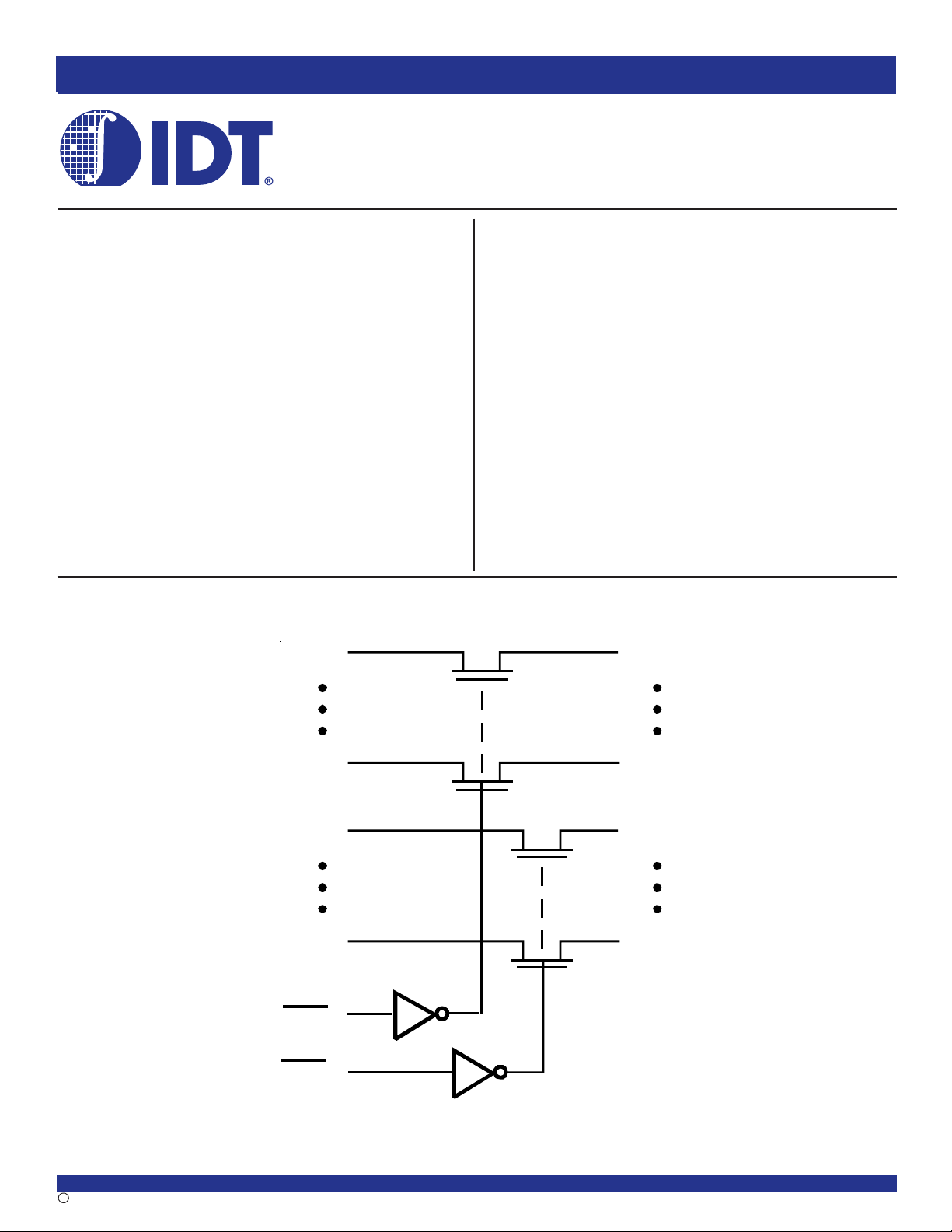
Ω bidirectional switches connect inputs to outputs
ΩΩ
• Zero propagation delay, zero added ground bounce
• Undershoot clamp diodes on all switch and control inputs
• Two enables control five bits each
• Available in SOIC, QSOP, and TSSOP packages
APPLICA TIONS:
• Hot-swapping, hot-docking
• Voltage translation (5V to 3.3V)
• Power Conservation
• Capacitance reduction and isloation
• Bus Isolation
• Clock Gating
IDTQS3384
DESCRIPTION:
The QS3384 provides a set of ten high-speed CMOS, TTL-compatible
bus switches. The low ON resistance of QS3384 allows inputs to be
connected to outputs without adding propagation delay and without generating additional ground bounce. Two banks of 5 switches are controlled by
independent Bus Enable (BE) signals.
The QS3384 is characterized for operation at -40°C to +85°C.
FUNCTIONAL BLOCK DIAGRAM
A0
A4
A5
A9
BEA
B0
B4
B5
B9
BEB
The IDT logo is a registered trademark of Integrated Device Technology, Inc.
INDUSTRIAL TEMPERATURE RANGE
2000 Integrated Device Technology, Inc. DSC-5758/1c
FEBRUARY 2000
1
IDTQS3384
HIGH-SPEED CMOS 10-BIT BUS SWITCH
INDUSTRIAL TEMPERATURE RANGE
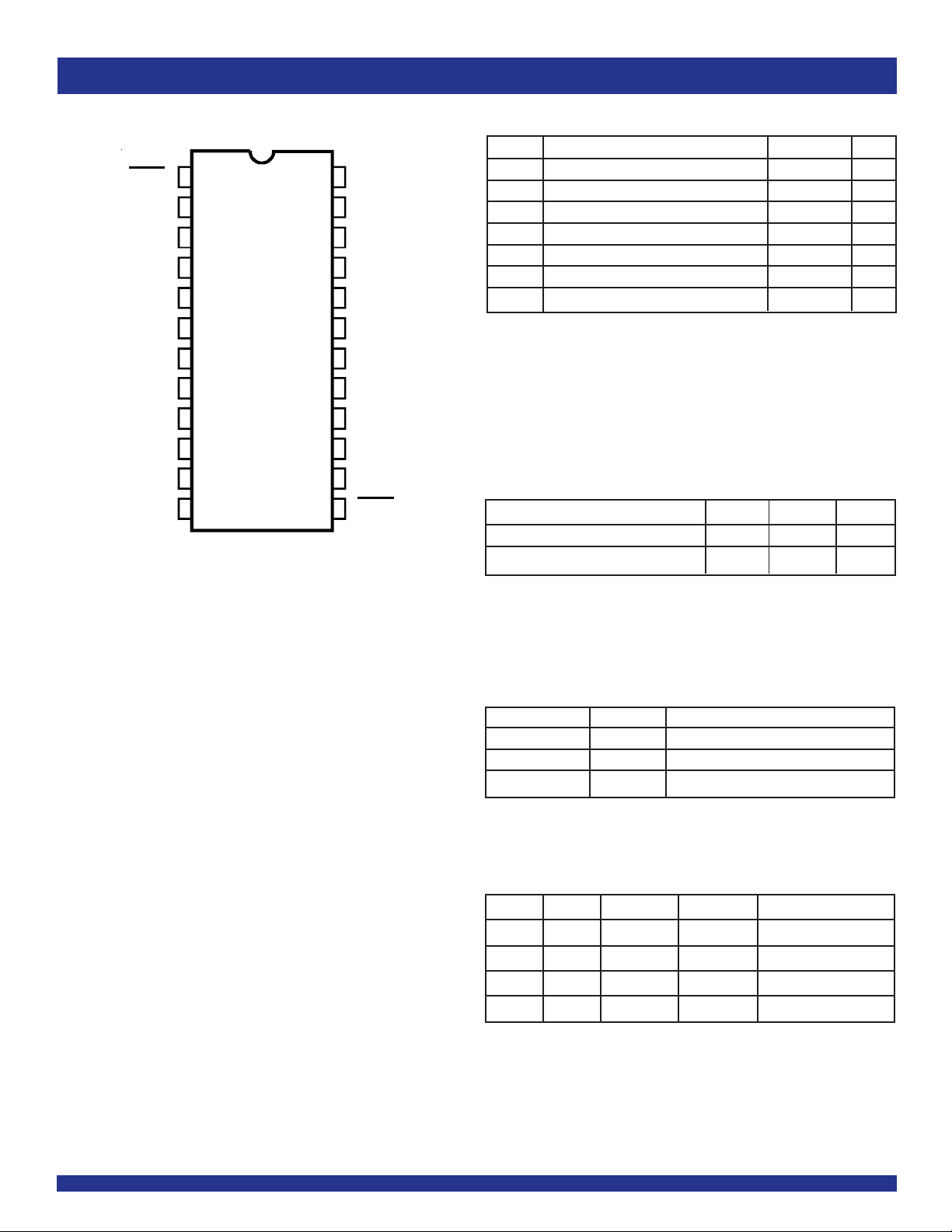
PIN CONFIGURATION
BEA
B
A0
A1
B1
B2
A2
A3
B3
B4
A4
GND
1
2
0
3
4
5
6
7
8
9
10
11
12
SOIC/ QSOP/ TSSOP
TOP VIEW
24
23
22
21
20
19
18
17
16
15
14
13
CC
V
B9
A9
A8
B8
B7
A7
A6
B6
B5
A5
BEB
ABSOLUTE MAXIMUM RATINGS
Symbol Description Max Unit
(2)
VTERM
VTERM
VTERM
VAC AC Input Voltage (pulse width ≤20ns) – 3 V
IOUT DC Output Current 120 mA
PMAX Maximum Power Dissipation (TA = 85°C) 0.5 W
T
STG Storage Temperature –65 to +150 °C
NOTES:
1. Stresses greater than those listed under ABSOLUTE MAXIMUM RATINGS may cause
permanent damage to the device. This is a stress rating only and functional operation
of the device at these or any other conditions above those indicated in the operational
sections of this specification is not implied. Exposure to absolute maximum rating
conditions for extended periods may affect reliability.
2. VCC terminals.
3. All terminals except VCC .
Supply Voltage to Ground –0.5 to +7 V
(3)
DC Switch Voltage VS –0.5 to +7 V
(3)
DC Input Voltage VIN –0.5 to +7 V
(1)
CAPACITANCE (TA = +25°C, f = 1MHz, VIN = 0V, VOUT = 0V)
Pins Typ. Max.
Control Inputs 3 5 pF
Quickswitch Channels (Switch OFF) 5 7 p F
NOTE:
1. This parameter is guaranteed but not production tested.
(1)
Unit
PIN DESCRIPTION
Pin Names I/ O Description
A0 - A9 I/O Bus A
B0 - B9 I/O Bus B
BEA, BEB I Bus Switch Enable
FUNCTION TABLE
BEA BEB B0 - A4 B5 - B9 Function
H H Hi-Z Hi-Z Disconnect
LH A0 - A4 Hi-Z Connect
H L Hi-Z A5 - A9 Connect
LLA
NOTE:
1. H = HIGH Voltage Level
L = LOW Voltage Level
Z = High-Impedance
(1)
0 - A4 A5 - A9 Connect
2
 Loading...