

PRELIMINARY DATASHEET
0.5Ω LOW VOLTAGE, SINGLE SPDT ANALOG SWITCH
Description
The IDTAS4624 low on-resistance (RON), low voltage,
single-pole/double-throw (SPDT) analog switch operates
from a single +1.8 V to +5.5 V supply. The IDTAS4624
features a 0.5Ω (max) RON for its NC switch and a 0.8Ω
(max) RON for its NO switch at a +2.7 V supply. It also
features break-before-make switching action (2 ns) with
t
= 50 ns and t
ON
is 1.8 V logic-compatible with a +2.7 V to +3.3 V supply.
= 40 ns at +3 V. The digital logic input
OFF
Applications
• Speaker headset switching
• MP3 players
• Battery-operated equipment
• Audio and video signal routing
• PCMCIA cards
• Cellular phones
• Modems
Features
• +1.8 V to +5.5 V single-supply operation
• Rail-to-rail signal handling
• 1.8 V logic compatibility
• RON match between channels: 0.06Ω (max)
• RON flatness over signal range: 0.15Ω (max)
• NCx Switch RON: 0.5Ω max (+2.7 V Supply) (ICSAS4684)
• NOx Switch RON: 0.8Ω max (+2.7 V Supply)
• Low crosstalk: -68dB (100 kHz)
• High Off-isolation: -64dB (100 kHz)
• THD: 0.03%
• 50 nA (max) supply current
• Low leakage currents: 1 nA (max) at TA = +25°C
• 6-pin SOT-23 package
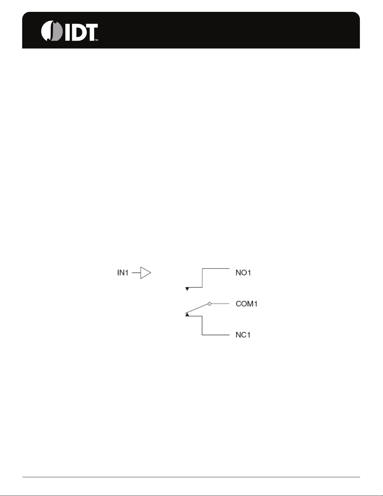
IDTAS4624
Block Diagram
IDT™
0.5Ω LOW VOLTAGE, SINGLE SPDT ANALOG SWITCH 1
IDTAS4624 REV B 061307
IDTAS4624
0.5Ω LOW VOLTAGE, SINGLE SPDT ANALOG SWITCH ANALOG SWITCH
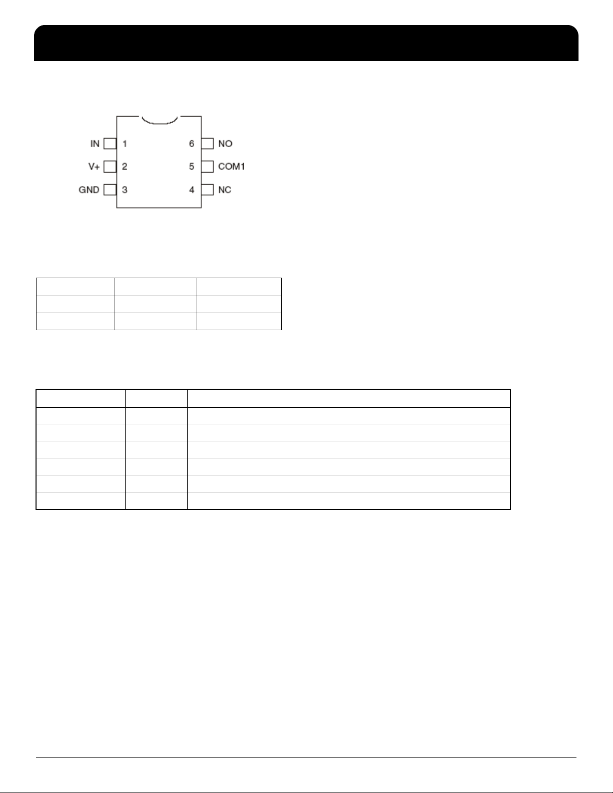
Pin Assignment (SOT-23)
Truth Table
IN1 NO1 NC1
0ONOFF
1OFFON
Note: Switches shown for logic “0” input.
Pin Descriptions
Pin Numbers Pin Name Pin Description
4 NC Analog switch. Normally closed terminal.
1 IN Digital control input.
5 COM1 Analog switch. Common terminal 1.
6 NO Analog switch. Normally open terminal.
2 V+ Positive supply voltage input.
3 GND Ground.
IDT™
0.5Ω LOW VOLTAGE, SINGLE SPDT ANALOG SWITCH 2
IDTAS4624 REV B 061307

IDTAS4624
0.5Ω LOW VOLTAGE, SINGLE SPDT ANALOG SWITCH ANALOG SWITCH
Absolute Maximum Ratings
Stresses above the ratings listed below can cause permanent damage to the IDTAS4624. These ratings, which are
standard values for IDT commercially rated parts, are stress ratings only. Functional operation of the device at these
or any other conditions above those indicated in the operational sections of the specifications is not implied.
Exposure to absolute maximum rating conditions for extended periods can affect product reliability. Electrical
parameters are guaranteed only over the recommended operating temperature range. All voltages referenced to
ground.
Symbol Rating Min Max Unit
V+, IN -0.3 +6 V
COM, NO, NC -0.3 (V+ + 0.3) V
Continuous current ±300
NO, NC, COM
Peak current (pulsed at 1ms, 10% duty cycle) ±500
Continuous power dissipation (TA = +70°C) and
12-bump UCSP (derate 11.4mW/°C above +70°C)
Operating temperature range 0 +70 °C
TSTG Storage temperature range -65 +150 °C
Lead temperature (soldering, 10s) +300 °C
Bump temperature (soldering, infrared, 15s) +200 °C
Vapor phase (60s) +215 °C
+909 mW
mAPeak current (pulsed at 1ms, 50% duty cycle) ±400
IDT™
0.5Ω LOW VOLTAGE, SINGLE SPDT ANALOG SWITCH 3
IDTAS4624 REV B 061307
IDTAS4624
0.5Ω LOW VOLTAGE, SINGLE SPDT ANALOG SWITCH ANALOG SWITCH
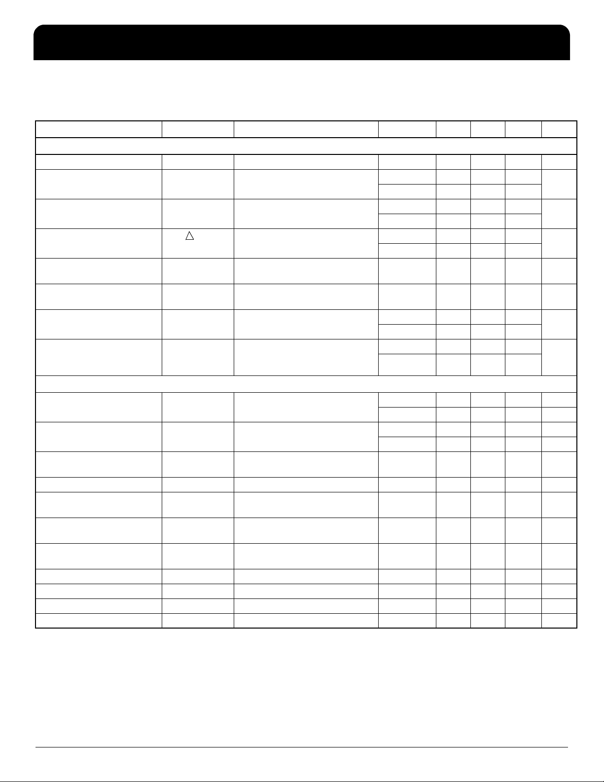
Electrical Characteristics, +3 V Supply (notes 1, 2)
Unless stated otherwise, V+ = 2.7 V to 3.3 V, VIH = 1.4 V, VIL = 0.5 V, TA = T
Parameter Symbol Conditions T
Analog Switch
Analog Signal Range VNO, V
NC On-Resistance R
NO On-Resistance R
On-Resistance Match
between channels
NC On-Resistance Flatness R
NO On-Resistance Flatness R
NO or NC Off-leakage Current I
COM On-leakage Current I
NC, VCOM
ON(NC)
V+ = 2.7 V, I
COM
= 100 mA,
VNC = 0 to V+; Note 3
ON(NO)
V+ = 2.7 V, I
COM
= 100 mA,
VNO = 0 to V+; Note 3
R
ON
V+ = 2.7 V, I
COM
= 100 mA,
VNO or VNC = 1.5 V; Notes 3, 4
FLAT(NC)
V+ = 2.7 V, I
COM
= 100 mA,
VNC = 0 to V+; Note 5
FLAT(NO)
(OFF) or
NO
INC(OFF)
(ON) V+ = 3.3 V, VNO or VNC = 3 V, 0.3
COM
V+ = 2.7 V, I
= 0 to V+; Note 5
V
NO
V+ = 3.3 V, VNO or VNC = 3 V, 0.3 V
V
= 0.3 V, 3 V
COM
COM
= 100 mA,
V, or floating
V
= 0.3 V, 3 V, or floating
COM
Dynamic Characteristics
Turn-on Time t
Turn-off Time t
Break-Before-Make-Delay t
ON
OFF
BBM
Charge Injection Q COM = 0, RS = 0, C
Off-Isolation V
Crosstalk V
ISO
CT
Total Harmonic Distortion THD R
NC Off-Capacitance C
NC Off-Capacitance C
NC On-Capacitance C
NC On-Capacitance C
(OFF) f = 1 MHz +25°C 84 pF
NC
(OFF) f = 1 MHz +25°C 37 pF
NO
(ON) f = 1 MHz +25°C 190 pF
NC
(ON) f = 1 MHz +25°C 150 pF
NO
V+ = 2.7 V, VNO or VNC = 1.5 V,
RL = 50Ω, CL = 35 pF
V+ = 2.7 V, VNO or VNC = 1.5 V,
RL = 50Ω, CL = 35 pF
V+ = 2.7 V, VNO or VNC = 1.5 V,
RL = 50Ω, CL = 35 pF
= 1 nF +25°C 200 pC
L
CL = 5 pF; RL = 50Ω, f = 100 kHz,
V
COM
= 1 V
RMS
, Note 6
f = 100 kHz, RL = 50Ω, CL = 5 pF,
= 1 V
V
COM
= 600Ω, IN = 2 V p-p,
L
RMS
f = 20Hz to 20 kHz
MIN
to T
. Typical values are at +3 V and 25°C
MAX
A
T
MIN to TMAX
Min. Typ. Max. Units
0V+V
+25°C 3.0 0.5 Ω
T
MIN to TMAX
+25°C 0.45 0.8 Ω
T
MIN to TMAX
+25°C 0 0.6 Ω
T
MIN to TMAX
T
MIN to TMAX
T
MIN to TMAX
+25°C -1 +1 nA
T
MIN to TMAX
-10 +10
+25°C -2 +2 nA
T
MIN to TMAX
-20 +20
+25°C 30 50 ns
T
MIN to TMAX
+25°C 25 30 ns
T
MIN to TMAX
T
MIN to TMAX
215 ns
+25°C -64 dB
+25°C -68 dB
+25°C 0.03 %
0.5
0.8
0.6
0.15 Ω
0.35 Ω
60 ns
40 ns
IDT™
0.5Ω LOW VOLTAGE, SINGLE SPDT ANALOG SWITCH 4
IDTAS4624 REV B 061307
IDTAS4624
0.5Ω LOW VOLTAGE, SINGLE SPDT ANALOG SWITCH ANALOG SWITCH
Parameter Symbol Conditions T
Digital I/O
Input Logic HIGH V
Input Logic LOW V
IN Input Leakage Current I
IH
IL
IN
VIN = 0 or V+
Power Supply
Power Supply Range V+ T
Supply Current I+
Notes:
1. The algebraic convention used in this data sheet is where the most negative value is a minimum and the most positive value
a maximum.
2. UCSP parts are 100% tested at +25°C only and guaranteed by design and correlation at the full hot-rated temperature.
3. Guaranteed by design.
4. R
ON
= R
ON(MAX)
- R
ON(MIN)
5. Flatness is defined as the difference between the maximum and minimum value of on resistance as measured over the
specified analog signal ranges.
6. Off-isolation = 20log10 (V
COM
, between NC1 and NC2 or between NO1 and NO2.
/ VCO), V
V+ = 5.5 V, VIN = 0 or V+,
Note 3
= output, VCO = input to off switch.
COM
Min. Typ. Max. Units
1.4 V
0.5 V
-1 1 µA
1.8 5.5 V
T
MIN to
T
MAX
T
MIN to
T
MAX
T
MIN to
T
MAX
MIN to
T
MAX
A
+25°C -50 +0.04 +50 nA
T
MIN to
T
MAX
-200 +200
IDT™
0.5Ω LOW VOLTAGE, SINGLE SPDT ANALOG SWITCH 5
IDTAS4624 REV B 061307

IDTAS4624
0.5Ω LOW VOLTAGE, SINGLE SPDT ANALOG SWITCH ANALOG SWITCH
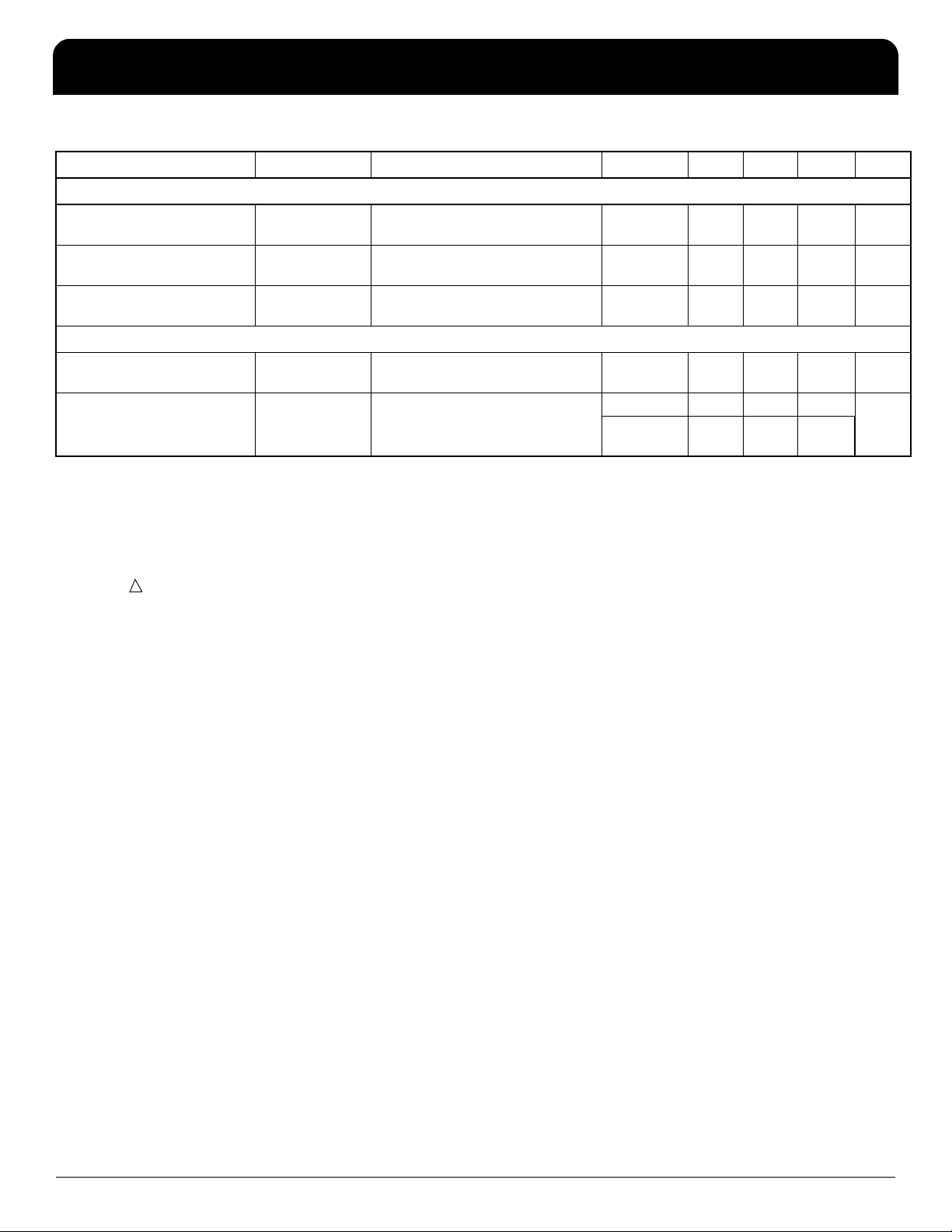
Electrical Characteristics, +5 V Supply (Note 1)
Unless stated otherwise, V+ = 5 V ±10%, GND = 0, VIH = +2.4 V, VIL = +0.8 V, TA = T
Parameter Symbol Conditions T
Analog Switch
Analog Signal Range VNO, V
On-Resistance R
On-Resistance Match
between channels
On-Resistance Flatness R
NO or NC Off-leakage Current I
COM On-leakage Current I
Overcurrent-Protection
Current Threshold
NC, VCOM
ON
R
ON
FLAT(ON)
(OFF) or
NO
INC(OFF)
(ON) V+ = 5.5 V, VNO or VNC = 1 V,
COM
V+ = 4.5 V, I
VNC or V
NO
V+ = 4.5 V, I
VNC or V
NO
V+ = 4.5 V, I
VNC or V
NO
V+ = 5.5 V, VNO or VNC = 1 V, 4.5 V
V
= 1 V, 4.5 V
COM
= 100 mA,
COM
= 3.5 V
= 100 mA,
COM
= 3.5 V
= 100 mA,
COM
= 0V, 1 V, 2 V, Note 3
4.5 V, or floating
= 1 V, 4.5 V
V
COM
= +25°C 1.2 A
T
A
Dynamic Characteristics
Turn-on Time t
Turn-off Time t
Break-Before-Make-Delay t
ON
OFF
BBM
Charge Injection Q V
Off-Isolation O
Crosstalk V
NC or NO Off-Capacitance C
COM On-Capacitance C
IRR
CT
OFF
(ON) f = 1 MHz +25°C 190 pF
COM
VNO or VNC = 3 V +25°C 40 50 ns
VNO or VNC = 3 V +25°C 40 50 ns
Note 4 +25°C 1 20 ns
GEN
= 0, R
= 0, CL = 1 nF +25°C 200 pC
GEN
CL = 5 pF; RL = 50Ω, f = 1 MHz +25°C -64 dB
CL = 5 pF; RL = 50Ω, f = 1 MHz,
Note 5
f = 1 MHz +25°C 37 pF
MIN
to T
. Typical values are at +3 V and +25°C
MAX
A
Min. Typ. Max. Units
0V+V
+25°C 0.65 1 Ω
T
MIN to TMAX
+25°C 0.6 0.12 Ω
T
MIN to TMAX
+25°C 0.8 0.12 Ω
T
MIN to TMAX
+25°C -2 0.01 +2 nA
T
MIN to TMAX
-20 +20
+25°C -4 0.3 +4 nA
T
MIN to TMAX
T
MIN to TMAX
T
MIN to TMAX
T
MIN to TMAX
-40 +40
1
+25°C -68 dB
1.2
0.15
0.15
60
60
IDT™
0.5Ω LOW VOLTAGE, SINGLE SPDT ANALOG SWITCH 6
IDTAS4624 REV B 061307

IDTAS4624
0.5Ω LOW VOLTAGE, SINGLE SPDT ANALOG SWITCH ANALOG SWITCH
Parameter Symbol Conditions T
A
Min. Typ. Max. Units
Logic Input
Input Voltage HIGH V
Input Voltage LOW V
Logic Input Current I
INH
INL
IN
2.4 V
0.8 V
-1 +1 µA
Power Supply
Power Supply Range V+ 1.8 5.5 V
Positive Supply Current I+
Notes:
1. The algebraic convention used in this data sheet is where the most negative value is a minimum and the most positive value
a maximum.
2. Guaranteed by design.
3. R
ON
= R
ON(MAX)
- R
ON(MIN)
4. Flatness is defined as the difference between the maximum and minimum value of on resistance as measured over the
specified analog signal ranges.
5. Off-isolation = 20log10 (V
COM
, between NC1 and NC2 or between NO1 and NO2.
/ VCO), V
V+ = 5.5 V, VIN = 0 or V+ 10 nA
= output, VCO = input to off switch.
COM
IDT™
0.5Ω LOW VOLTAGE, SINGLE SPDT ANALOG SWITCH 7
IDTAS4624 REV B 061307

IDTAS4624
0.5Ω LOW VOLTAGE, SINGLE SPDT ANALOG SWITCH ANALOG SWITCH
Test Circuits and Timing Diagrams
Overvoltage Protection Using Two External Blocking Diodes
IDT™
0.5Ω LOW VOLTAGE, SINGLE SPDT ANALOG SWITCH 8
Switching Time
IDTAS4624 REV B 061307

IDTAS4624
0.5Ω LOW VOLTAGE, SINGLE SPDT ANALOG SWITCH ANALOG SWITCH
Break-Before-Make Interval
IDT™
0.5Ω LOW VOLTAGE, SINGLE SPDT ANALOG SWITCH 9
Charge Injection
IDTAS4624 REV B 061307

IDTAS4624
0.5Ω LOW VOLTAGE, SINGLE SPDT ANALOG SWITCH ANALOG SWITCH
On-Loss, Off-Isolation, and Crosstalk
Channel Off/On Capacitance
IDT™
0.5Ω LOW VOLTAGE, SINGLE SPDT ANALOG SWITCH 10
IDTAS4624 REV B 061307

IDTAS4624
0.5Ω LOW VOLTAGE, SINGLE SPDT ANALOG SWITCH ANALOG SWITCH
Marking Diagram (SOT-23)
TBD
Notes:
1. “Z” is the device step (1 to 2 characters).
2. YYWW is the last two digits of the year and week that the part was assembled.
3. “$” is the assembly mark code.
4. “G” after the two-letter package code designates RoHS compliant package.
5. “I” at the end of part number indicates industrial temperature range.
6. Bottom marking: country of origin if not USA.
IDT™
0.5Ω LOW VOLTAGE, SINGLE SPDT ANALOG SWITCH 11
IDTAS4624 REV B 061307

IDTAS4624
0.5Ω LOW VOLTAGE, SINGLE SPDT ANALOG SWITCH ANALOG SWITCH
Package Outline and Package Dimensions (SOT-23-6)
Package dimensions are kept current with JESD Publication No. 95-1,
Millimeters Inches
Symbol Min Max Min Max
A 0.90 1.45 .0354 .0571
A1 0 0.15 0 .0059
A2 0.90 1.30 .0354 .0512
b 0.35 0.50 .0138 .0197
c 0.09 0.22 .0036 .0087
D 2.80 3.00 .1102 .1181
E 2.60 3.00 .1024 .1181
E1 1.50 1.75 .0591 .0689
e 0.95 BASIC 0.0374 BASIC
e1 1.90 BASIC 0.0748 BASIC
L 0.35 0.55 .0138 .0217
L1 0.50 0.70 .0197 .0276
L2 0.25 BASIC .0098 BASIC
θ
aaa — 0.10 — .0039
0° 10° 0° 10°
IDT™
0.5Ω LOW VOLTAGE, SINGLE SPDT ANALOG SWITCH 12
IDTAS4624 REV B 061307

IDTAS4624
0.5Ω LOW VOLTAGE, SINGLE SPDT ANALOG SWITCH ANALOG SWITCH
Ordering Information
IDT
XXXXXX
Device Type
XXX
Package
X
Temp. Range
X
Shipping
Carrier
8 Tape and Reel
Blank Tray
Blank Commercial (0 to +70°C)
DZG SOT-23 Package
AS4624 0.5Ω Low Voltage,
Single SPDT Analog Switch
IDT™
0.5Ω LOW VOLTAGE, SINGLE SPDT ANALOG SWITCH 13
IDTAS4624 REV B 061307

IDTAS4624
0.5Ω LOW VOLTAGE, SINGLE SPDT ANALOG SWITCH ANALOG SWITCH
Revision History
Rev. Originator Date Description of Change
B 6/12/07 Created datasheet in new template; added marking diagram.
IDT™
0.5Ω LOW VOLTAGE, SINGLE SPDT ANALOG SWITCH 14
IDTAS4624 REV B 061307

IDTAS4624
0.5Ω LOW VOLTAGE, SINGLE SPDT ANALOG SWITCH ANALOG SWITCH
Innovate with IDT and accelerate your future networks. Contact:
www.IDT.com
For Sales
800-345-7015
408-284-8200
Fax: 408-284-2775
Corporate Headquarters
Integrated Device Technology, Inc.
www.idt.com
© 2006 Integrated Device Technology, Inc. All rights reserved. Product specifications subject to change without notice. IDT an d the IDT logo are trademarks of Integrated Device
Technology, Inc. Accel erated Thinking is a service mark of Integrated Device Technology, Inc. All other brands, product names and marks are or ma y be trademarks or registered
trademarks used to identify products or services of their respective owners.
Printed in USA
For Tech Support
408-284-4522
www.idt.com/go/clockhelp
 Loading...