

QUAD PROGRAMMABLE PCM
CODEC WITH MPI INTERFACE
IDT82V1054A
FEATURES
• 4-channel CODEC with on-chip digital filters
• Software selectable A/
µ-law, linear code conversion
• Meets ITU-T G.711 - G.714 requirements
• Programmable digital filters adapting to system demands:
- AC impedance matching
- Transhybrid balance
- Frequency response correction
- Gain setting
• Supports two programmable PCM buses
• Flexible PCM interface with up to 128 programmable time slots,
data rate from 512 kbits/s to 8.192 Mbits/s
• MPI control interface
• Broadcast mode for coefficient setting
• 7 SLIC signaling pins (including 2 debounced pins) per channel
• Fast hardware ring trip mechanism
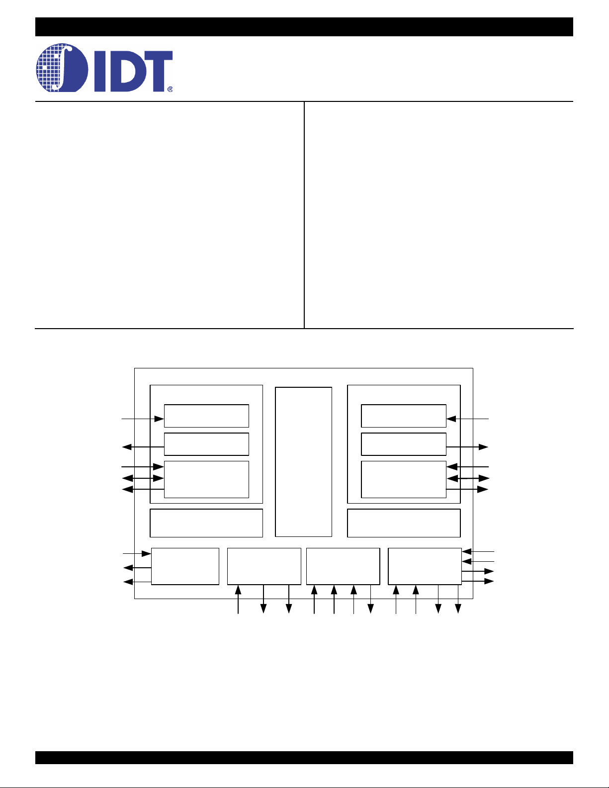
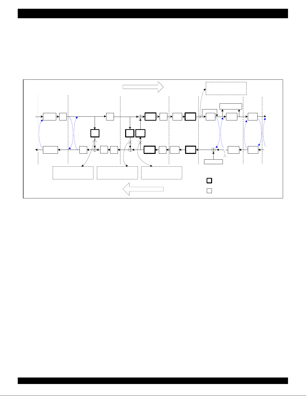
FUNCTIONAL BLOCK DIAGRAM
CH1
• 2 programmable tone generators per channel for testing,
ringing and DTMF generation
• Two programmable chopper clocks
• Master clock frequency selectable: 1.536 MHz, 1.544 MHz, 2.048
MHz, 3.072 MHz, 3.088 MHz, 4.096 MHz, 6.144 MHz, 6.176 MHz or
8.192 MHz
• Advanced test capabilities:
- 3 analog loopback tests
- 5 digital loopback tests
- Level metering function
• High analog driving capability (300 Ω AC)
• 3 V digital I/O with 5 V tolerance
• CODEC identification
• +3.3 V single power supply
• Low power consumption
• Operating temperature range: -40°C to +85°C
• Package available: 64 Pin TQFP
CH3
VIN1
VOUT1
2 Inputs
3 I/Os
2 Outputs
MCLK
CHCLK1
CHCLK2
Filter and A/D
D/A and Filter
SLIC Signaling
CH2
PLL and Clock
Generation
General Control
Logic
RESET INT12
DSP
Core
CCLK
MPI Interface
CI
Filter and A/D
D/A and Filter
SLIC Signaling
CH4
FS
CO CSINT34
PCM Interface
TSX1
BCLK
VIN3
VOUT3
2 Inputs
3 I/Os
2 Outputs
DR1
DR2
DX1
DX2
TSX2
The IDT logo is a registered trademark of Integrated Device Technology, Inc.
INDUSTRIAL TEMPERATURE RANGE
2004 Integrated Device Technology, Inc.
JULY 19, 2004
1
DSC-6223/4
IDT82V1054A QUAD PROGRAMMABLE PCM CODEC WITH MPI INTERFACE INDUSTRIAL TEMPERATURE
DESCRIPTION
The IDT82V1054A is a feature rich, single-chip, programmable 4-
channel PCM CODEC with on-chip filters. Besides the
µ-Law/A-Law
companding and linear coding/decoding (14 effective bits + 2 extra sign
bits), the IDT82V1054A also provides 2 programmable tone generators
per channel (which can generate ring signals) and 2 programmable
chopper clocks for SLICs.
The digital filters in the IDT82V1054A provide necessary transmit
and receive filtering for voice telephone circuits to interface with timedivision multiplexed systems. An integrated programmable DSP realizes
AC impedance matching, transhybrid balance, frequency response
correction and gain adjustment functions. The IDT82V1054A supports 2
PCM buses with programmable sampling edge, which allows an extra
delay of up to 7 clocks. Once the delay is determined, it is effective to all
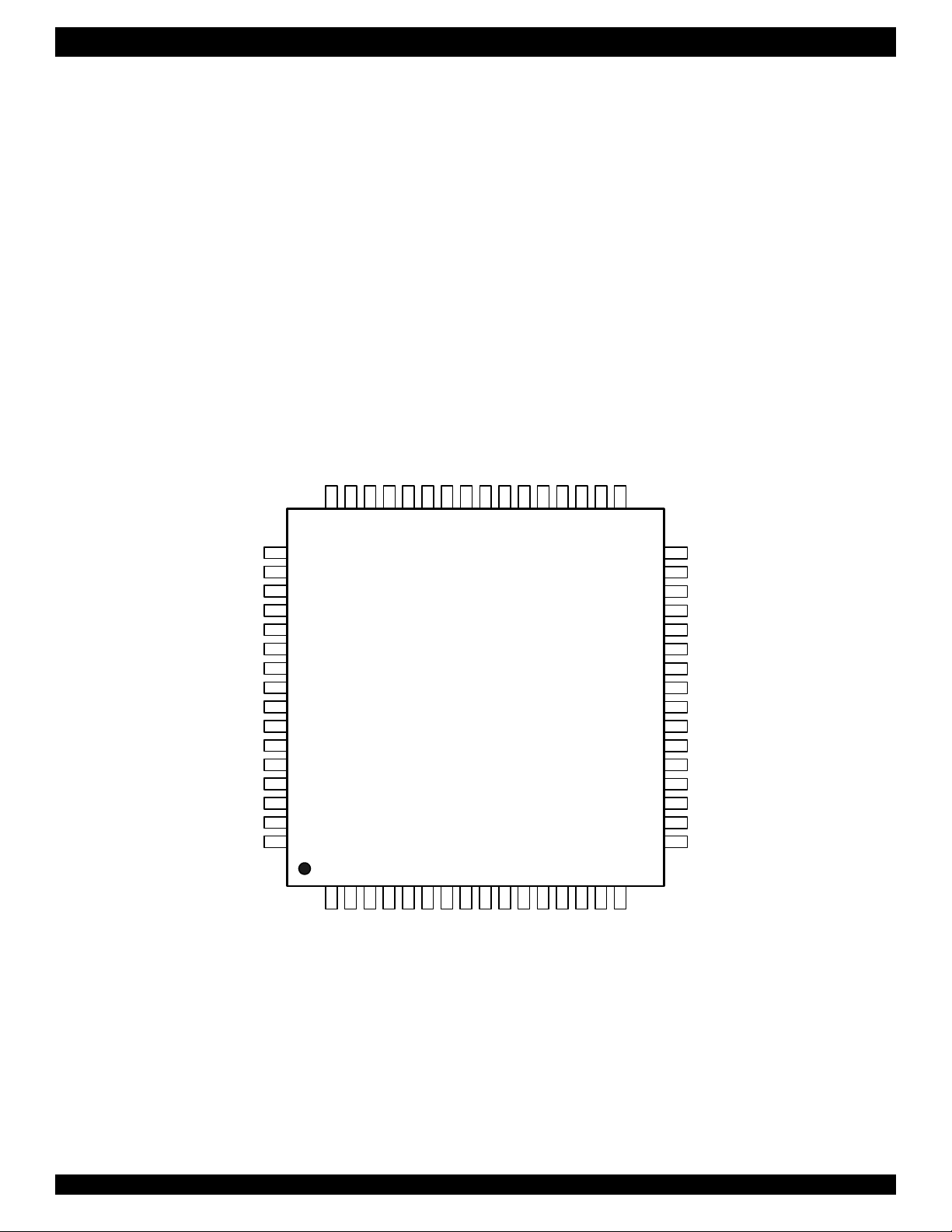
PIN CONFIGURATION
SI2_2
SI1_2
SB3_2
SB2_2
SB1_2
SO2_2
484746454443424140393837363534
four channels of the IDT82V1054A. The device also provides 7 signaling
pins per channel for SLICs.
The IDT82V1054A is programmed via a Microprocessor Interface
(MPI). Two PCM buses are provided to transfer the compressed or
linear PCM data.
The device offers strong test capability with several analog/digital
loopbacks and level metering function. It brings convenience to system
maintenance and diagnosis.
A unique feature of “Hardware Ring Trip” is implemented in the
IDT82V1054A. When an off-hook signal is detected, the IDT82V1054A
will reverse an output pin to stop the ringing signal immediately.
The IDT82V1054A can be used in digital telecommunication
applications such as Central Office Switch, PBX, DLC and Integrated
Access Devices (IADs), i.e. VoIP and VoDSL.
SO1_2
SO1_1
SO2_1
SB1_1
SB2_1
SB3_1
SI1_1
SI2_1
INT12
CHCLK1
33
VIN1
GNDA1
VOUT1
VDDA12
VOUT2
GNDA2
VIN2
CNF
VDDB
VIN3
GNDA3
VOUT3
VDDA34
VOUT4
GNDA4
VIN4
49
50
51
52
53
54
55
56
57
58
59
60
61
62
63
64
1
SI2_3
2
SI1_3
3
4
SB3_3
SB2_3
IDT82V1054A
64 Pin TQFP
5
6
7
8
9
10111213141516
SB1_3
SO2_3
SO1_3
SO1_4
SO2_4
SB1_4
SB2_4
SB3_4
SI1_4
SI2_4
INT34
32
31
30
29
28
27
26
25
24
23
22
21
20
19
18
17
CHCLK2
BCLK
FS
DR2
DX2
TSX2
DR1
DX1
TSX1
VDDD
RESET
MCLK
GNDD
CO
CI
CCLK
CS
2

IDT82V1054A QUAD PROGRAMMABLE PCM CODEC WITH MPI INTERFACE INDUSTRIAL TEMPERATURE
TABLE OF CONTENTS
1 Pin Description...................................................................................................................................................................................................7
2 Functional Description ......................................................................................................................................................................................9
2.1 MPI/PCM Interface ....................................................................................................................................................................................9
2.1.1 Microprocessor Interface (MPI) ....................................................................................................................................................9
2.1.2 PCM Bus ....................................................................................................................................................................................10
2.2 DSP Programming...................................................................................................................................................................................11
2.2.1 Signal Processing.......................................................................................................................................................................11
2.2.2 Gain Adjustment.........................................................................................................................................................................11
2.2.3 Impedance Matching .................................................................................................................................................................11
2.2.4 Transhybrid Balance ..................................................................................................................................................................12
2.2.5 Frequency Response Correction................................................................................................................................................12
2.3 SLIC Control ............................................................................................................................................................................................12
2.3.1 SI1 and SI2.................................................................................................................................................................................12
2.3.2 SB1, SB2 and SB3 .....................................................................................................................................................................12
2.3.3 SO1 and SO2 .............................................................................................................................................................................12
2.4 Hardware Ring Trip .................................................................................................................................................................................12
2.5 Interrupt and Interrupt Enable..................................................................................................................................................................12
2.6 Debounce Filters .....................................................................................................................................................................................13
2.7 Chopper Clock.........................................................................................................................................................................................13
2.8 Dual Tone and Ring Generation..............................................................................................................................................................13
2.9 Level Metering .........................................................................................................................................................................................14
2.10 Channel Power Down/Standby Mode......................................................................................................................................................14
2.11 Power Down/Suspend Mode ...................................................................................................................................................................14
3 Operating The IDT82V1054A...........................................................................................................................................................................15
3.1 Programming Description ........................................................................................................................................................................15
3.1.1 Command Type and Format ......................................................................................................................................................15
3.1.2 Addressing the Local Registers..................................................................................................................................................15
3.1.3 Addressing the Global Registers................................................................................................................................................15
3.1.4 Addressing the Coe-RAM...........................................................................................................................................................15
3.1.5 Programming Examples .............................................................................................................................................................16
3.1.5.1 Example of Programming Local Registers .................................................................................................................16
3.1.5.2 Example of Programming Global Registers................................................................................................................16
3.1.5.3 Example of Programming the Coefficient-RAM..........................................................................................................16
3.2 Power-on Sequence ................................................................................................................................................................................19
3.3 Default State After Reset.........................................................................................................................................................................19
3.4 Registers Description ..............................................................................................................................................................................20
3.4.1 Registers Overview ....................................................................................................................................................................20
3.4.2 Global Registers List ..................................................................................................................................................................22
3.4.3 Local Registers List ....................................................................................................................................................................28
4 Absolute Maximum Ratings............................................................................................................................................................................32
5 Recommended DC Operating Conditions .....................................................................................................................................................32
6 Electrical Characteristics ................................................................................................................................................................................32
6.1 Digital Interface........................................................................................................................................................................................32
6.2 Power Dissipation....................................................................................................................................................................................32
6.3 Analog Interface ......................................................................................................................................................................................33
7 Transmission Characteristics.........................................................................................................................................................................34
7.1 Absolute Gain ..........................................................................................................................................................................................34
7.2 Gain Tracking ..........................................................................................................................................................................................34
7.3 Frequency Response ..............................................................................................................................................................................34
7.4 Group Delay ............................................................................................................................................................................................35
7.5 Distortion .................................................................................................................................................................................................35
7.6 Noise .......................................................................................................................................................................................................36
3

IDT82V1054A QUAD PROGRAMMABLE PCM CODEC WITH MPI INTERFACE INDUSTRIAL TEMPERATURE
7.7 Interchannel Crosstalk.............................................................................................................................................................................36
7.8 Intrachannel Crosstalk.............................................................................................................................................................................36
8 Timing Characteristics ....................................................................................................................................................................................37
8.1 Clock Timing............................................................................................................................................................................................37
8.2 Microprocessor Interface Timing .............................................................................................................................................................38
8.3 PCM Interface Timing..............................................................................................................................................................................39
9 Appendix: IDT82V1054A Coe-RAM Mapping.................................................................................................................................................40
10 Ordering Information .......................................................................................................................................................................................41
4

IDT82V1054A QUAD PROGRAMMABLE PCM CODEC WITH MPI INTERFACE INDUSTRIAL TEMPERATURE
LIST OF FIGURES
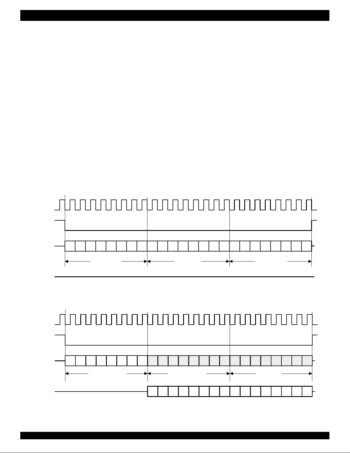
Figure - 1 An Example of the MPI Interface Write Operation .............................................................................................................................. 9
Figure - 2 An Example of the MPI Interface Read Operation (ID = 81H)............................................................................................................. 9
Figure - 3 Sampling Edge Selection Waveform................................................................................................................................................. 10
Figure - 4 Signal Flow for Each Channel........................................................................................................................................................... 11
Figure - 5 Debounce Filter................................................................................................................................................................................. 13
Figure - 6 Clock Timing...................................................................................................................................................................................... 37
Figure - 7 MPI Input Timing ............................................................................................................................................................................... 38
Figure - 8 MPI Output Timing ............................................................................................................................................................................ 38
Figure - 9 Transmit and Receive Timing............................................................................................................................................................ 39
Figure - 10 Typical Frame Sync Timing (2 MHz Operation) ................................................................................................................................ 39
Figure - 11 Coe-RAM Mapping............................................................................................................................................................................ 40
5

IDT82V1054A QUAD PROGRAMMABLE PCM CODEC WITH MPI INTERFACE INDUSTRIAL TEMPERATURE
LIST OF TABLES
Table - 1 Consecutive Adjacent Addressing......................................................................................................................................................15
Table - 2 Global Registers (GREG) Mapping....................................................................................................................................................20
Table - 3 Local Registers (LREG) Mapping.......................................................................................................................................................21
Table - 4 Coe-RAM Address Allocation.............................................................................................................................................................40
6

IDT82V1054A QUAD PROGRAMMABLE PCM CODEC WITH MPI INTERFACE INDUSTRIAL TEMPERATURE
1 PIN DESCRIPTION
Name Type Pin Number Description
GNDA1
GNDA2
GNDA3
Ground
GNDA4
GNDD Ground 21
VDDA12
VDDA34
Power
50
54
59
63
52
61
Analog Ground.
All ground pins should be connected together.
Digital Ground.
All digital signals are referred to this pin.
+3.3 V Analog Power Supply.
These pins should be connected to ground via a 0.1
connected together.
VDDD Power 24 +3.3 V Digital Power Supply.
+3.3 V Analog Power Supply.
VDDB Power 57
This pin should be connected to ground via a 0.1
together.
CNF − 56
VIN1-4 I 49, 55, 58, 64
VOUT1-4 O 51, 53, 60, 62
SI1_(1-4)
SI2_(1-4)
I
36, 47, 2, 13
35, 48, 1, 14
Capacitor Noise Filter.
This pin should be connected to ground via a 0.22
Analog Voice Inputs of Channel 1-4.
These pins should be connected to the corresponding SLIC via a 0.22
Voice Frequency Receiver Outputs of Channel 1-4.
These pins can drive 300 Ω AC load. It can drive transformers directly.
SLIC Signalling Inputs with debounce function for Channel 1-4.
µF capacitor. All power supply pins should be
µF capacitor. All power supply pins should be connected
µF capacitor.
µF capacitor.
SB1_(1-4)
SB2_(1-4)
SB3_(1-4)
SO1_(1-4)
SO2_(1-4)
I/O
O
39, 44, 5, 10
38, 45, 4, 11
37, 46, 3, 12
41, 42, 7, 8
40, 43, 6, 9
DX1 O26
DX2 O29
DR1 I27
DR2 I30
FS I31
BCLK I32
Bi-directional SLIC Signalling I/Os for Channel 1-4.
These pins can be individually programmed as input or output.
SLIC Signalling Outputs for Channel 1-4.
Transmit PCM Data Output, PCM Highway One.
Transmit PCM Data to PCM highway one. The PCM data is output through DX1 or DX2 as selected by
local register LREG5. This pin remains in high-impedance state until a pulse appears on the FS pin.
Transmit PCM Data Output, PCM Highway Two.
Transmit PCM Data to PCM highway two. The PCM data is output thought DX1 or DX2 as selected by
local register LREG5. This pin remains in high-impedance state until a pulse appears on the FS pin.
Receive PCM Data Input, PCM Highway One.
The PCM data is received from PCM highway one (DR1) or two (DR2). The receive PCM highway is
selected by local register LREG6.
Receive PCM Data Input, PCM Highway Two.
The PCM data is received from PCM highway one (DR1) or two (DR2). The receive PCM highway is
selected by local register LREG6.
Frame Synchronization.
FS is an 8 kHz synchronization clock that identifies the beginning of the PCM frame.
Bit Clock.
This pin clocks out the PCM data to DX1 or DX2 pin and clocks in PCM data from DR1 or DR2 pin. It may
vary from 512 kHz to 8.192 MHz and should be synchronous to FS.
7

IDT82V1054A QUAD PROGRAMMABLE PCM CODEC WITH MPI INTERFACE INDUSTRIAL TEMPERATURE
Name Type Pin Number Description
TSX1
TSX2
0
25
28
CS I17
CI I19
Transmit Output Indicator.
The TSX1 pin becomes low when PCM data is transmitted via DX1. Open-drain.
The TSX2 pin becomes low when PCM data is transmitted via DX2. Open-drain.
Chip Selection.
A logic low level on this pin enables the Serial Control Interface.
Serial Control Interface Data Input.
Control data input pin. CCLK determines the data rate.
Serial Control Interface Data Output.
CO O20
Control data output pin. CCLK determines the data rate. This pin is in high-impedance state when the CS
pin is logic high.
CCLK I18
Serial Control Interface Clock.
This is the clock for the Serial Control Interface. It can be up to 8.192 MHz.
Master Clock Input.
MCLK I22
This pin provides the clock for the DSP of the IDT82V1054A. The frequency of the MCLK can be 1.536
MHz, 1.544 MHz, 2.048 MHz, 3.072 MHz, 3.088 MHz, 4.096 MHz, 6.144 MHz, 6.176 MHz or 8.192 MHz.
RESET I23
Reset Input.
Forces the device to default mode. Active low.
Interrupt Output Pin for Channel 1-2.
INT12 O34
Active high interrupt signal for Channel 1 and 2, open-drain. It reflects the changes on the corresponding
SLIC input pins.
Interrupt Output Pin for Channel 3-4.
INT34 O15
Active high interrupt signal for Channel 3 and 4, open-drain. It reflects the changes on the corresponding
SLIC input pins.
CHCLK1 O33
CHCLK2 O16
Chopper Clock Output One.
Provides a programmable output signal (2 -28 ms) synchronous to MCLK.
Chopper Clock Output Two.
Provides a programmable output signal (256 kHz, 512 kHz or 16.384 MHz) synchronous to MCLK.
8
IDT82V1054A QUAD PROGRAMMABLE PCM CODEC WITH MPI INTERFACE INDUSTRIAL TEMPERATURE
2 FUNCTIONAL DESCRIPTION
The IDT82V1054A is a four-channel PCM CODEC with on-chip
digital filters. It provides a four-wire solution for the subscriber line
circuitry in digital switches. The IDT82V1054A converts analog voice
signals to digital PCM samples and digital PCM samples back to analog
voice signals. The digital filters are used to bandlimit the voice signals
during conversion. High performance oversampling Analog-to-Digital
Converters (ADC) and Digital-to-Analog Converters (DAC) in the
IDT82V1054A provide the required conversion accuracy. The
associated decimation and interpolation filtering is performed by both
dedicated hardware and Digital Signal Processor (DSP). The DSP also
handles all other necessary procession such as PCM bandpass filtering,
sample rate conversion and PCM companding.
2.1 MPI/PCM INTERFACE
A serial Microprocessor Interface (MPI) is provided for the master
device to control the IDT82V1054A. Two PCM buses are provided to
transfer the digital voice data.
2.1.1 MICROPROCESSOR INTERFACE (MPI)
The internal configuration registers (local/global), the SLIC signaling
interface and the Coefficient-RAM of the IDT82V1054A are programmed
by the master device via MPI, which consists of four lines (pins): CCLK,
CS, CI and CO. All commands and data are aligned in byte (8 bits) and
transferred via the MPI interface. CCLK is the clock of the MPI interface.
The frequency of CCLK can be up to 8.192 MHz. CS is the chip
selection pin. A low level on CS enables the MPI interface. CI and CO
are data input and data output pins, carrying control commands and
data bytes to/from the IDT82V1054A.
The data transfer is synchronized to the CCLK signal. The contents
of CI is latched on the rising edges of CCLK, while CO changes on the
falling edges of CCLK. The CCLK signal is the only reference of CI and
CO pins. Its duty and frequency may not necessarily be standard.
When the CS pin becomes low, the IDT82V1054A treats the first byte
on the CI pin as command and the rest as data. To write another
command, the CS pin must be changed from low to high to finish the
previous command and then changed from high to low to indicate the
start of a new command. When a read/write operation is completed, the
CS pin must be set to high in 8-bit time.
During the execution of commands that are followed by output data
byte(s), the IDT82V1054A will not accept any new commands from the
CI pin. But the data transfer sequence can be interrupted by setting the
CS pin to high at any time. See Figure - 1 and Figure - 2 for examples of
MPI write and read operation timing diagrams.
CCLK
CS
CI
CO
CCLK
CS
CI
7 6 5 4 3 2 1 0
Command Byte Data Byte 1 Data Byte 2
High 'Z'
Figure - 1 An Example of the MPI Interface Write Operation
7 6 5 4 3 2 1 0
7 6 5 4 3 2 1 0 7 6 5 4 3 2 1 0
Ignored
CO
High 'Z'
Command Byte Identification Code Data Byte 1
'0' '0' '0' '0' '0' '0' '1''1' 6 5 4 3 2 1 07
Figure - 2 An Example of the MPI Interface Read Operation (ID = 81H)
9
IDT82V1054A QUAD PROGRAMMABLE PCM CODEC WITH MPI INTERFACE INDUSTRIAL TEMPERATURE
2.1.2 PCM BUS
The IDT82V1054A provides two flexible PCM buses for all 4
channels. The digital PCM data can be compressed (A/
µ-law) or linear
code. As shown in Figure - 3, the data rate can be configured as same
as the Bit Clock (BCLK) or half of it. The PCM data is transmitted or
received either on the rising edges or on the falling edges of the BCLK
signal. The transmit and receive time slots can offset from the FS signal
by 0 to 7 periods of BCLK. All these configurations are made by global
register GREG7, which is effective for all four channels.
The PCM data of each channel can be assigned to any time slot of
the PCM bus. The number of available time slots is determined by the
frequency of the BCLK signal. For example, if the frequency is 512 kHz,
8 time slots (TS0 to TS7) are available. If the frequency is 1.024 MHz,
16 time slots (TS0 to TS15) are available. The IDT82V1054A accepts
BCLK frequency of 512 kHz to 8.192 MHz at increments of 64 kHz.
When compressed PCM code (8-bit wide) is selected, the voice data
of one channel occupies one time slot. The TT[6:0] bits in local register
LREG5 select the transmit time slot for each channel, while the RT[6:0]
bits in LREG6 select the receive time slot for each channel.
When linear PCM code is selected, the voice data is a 16-bit 2’s
FS
complement number (b13 to b0 are effective bits, b15 and b14 are as
same as the sign bit b13). So, the voice data of one channel occupies
one time slot group, which consists of 2 adjacent time slots. The TT[6:0]
bits in LREG5 select a transmit time slot group for the specified channel.
If TT[6:0] = n(d), it means that time slots TS(2n+1) and TS(2n+2) are
selected. For example, if TT[6:0] = 00H, it means that TS0 and TS1 are
selected. The RT[6:0] bits in LREG6 select a receive time slot group for
the specified channel in the same way.
The PCM data of each individual channel can be clocked out to
transmit PCM highway one (DX1) or two (DX2) on the programmed
edges of BCLK according to time slot assignment. The transmit PCM
highway is selected by the THS bit in LREG5. The frame sync (FS)
pulse identifies the beginning of a transmit frame (TS0). The PCM data
is serially transmitted on DX1 or DX2 with MSB first.
The PCM data of each individual channel is received from receive
PCM highway one (DR1) or two (DR2) on the programmed edges of
BCLK according to time slot assignment. The receive PCM highway is
selected by the RHS bit in LREG6. The frame sync (FS) pulse identifies
the beginning of a receive frame (TS0). The PCM data is serially
received from DR1 or DR2 with MSB first.
Transmit
Receive
BCLK
Single Clock
BCLK
Double Clock
PCM Clock Slope Bits
in GREG7:
CS = 000
CS = 001
CS = 010
CS = 011
Bit 7
TS0
CS = 100
CS = 101
CS = 110
CS = 111
Figure - 3 Sampling Edge Selection Waveform
10
IDT82V1054A QUAD PROGRAMMABLE PCM CODEC WITH MPI INTERFACE INDUSTRIAL TEMPERATURE
2.2 DSP PROGRAMMING
2.2.1 SIGNAL PROCESSING
Several blocks are programmable for signal processing. This allows
users to optimize the performance of the IDT82V1054A for the system.
Figure - 4 shows the signal flow for each channel and indicates the
programmable blocks.
The programmable digital filters are used to adjust gain and
Transmit Path
@64 KHz @16 KHz
IMF ECF
LREG1: CS[1]
CS[1] = 1: enable (normal)
CS[1] = 0: disable (cut)
Receive Path
VIN
VOUT
Analog @2 MHz
LPF/AA GTX D2 LPF FRX HPF CMP TSA
DLB-ANA
LPF/SC
∆−∑
DLB_1BIT
ALB-1BIT
LREG1: CS[2]
CS[2] = 1: enable (normal)
CS[2] = 0: disable (cut)
GIS
∆−∑
D1
U1
LREG1: CS[0]
CS[0] = 1: enable (normal)
CS[0] = 0: disable (cut)
impedance, balance transhybrid and correct frequency response. All the
coefficients of the digital filters can be calculated automatically by a
software provided by IDT. When users provide accurate SLIC model,
impedance and gain requirements, this software will calculate all the
coefficients automatically. After loading these coefficients to the
coefficient RAM of the IDT82V1054A, the final AC characteristics of the
line card (consists of SLIC and CODEC) will meet the ITU-T
specifications.
LREG1: CS[3]
CS[3] = 1: enable (normal)
CS[3] = 0: disable (bypass)
GRX U2 LPF FRR
@8 KHz
Level Meter
DLB-8K
ALB-8K
Dual Tone
CUT-OFF-PCM
Bold Black Framed: Programmable Filters
Fine Black Framed: Fixed Filters
TS PCM Highway
DLB-PCM
EXP TSAUF
ALB-DI
DX1/DX2
DLB-DI
DR1/DR2
Figure - 4 Signal Flow for Each Channel
Abbreviation List:
LPF/AA: Anti-Alias Low-pass Filter
LPF/SC: Smoothing Low-pass Filter
LPF: Low-pass Filter
HPF: High-pass Filter
GIS: Gain for Impedance Scaling
D1: 1st Down Sample Stage
D2: 2nd Down Sample Stage
U1: 1st Up Sample Stage
U2: 2nd Up Sample Stage
UF: Up Sampling Filter (64 k - 128 k)
2.2.2 GAIN ADJUSTMENT
For each individual channel, the analog A/D gain in the transmit path
can be selected as 0 dB or 6 dB. The selection is done by the GAD bit in
LREG9. It is 0 dB by default.
For each individual channel, the analog D/A gain in the receive path
can be selected as 0 dB or -6 dB. The selection is done by the GDA bit
in LREG9. It is 0 dB by default.
For each channel, the digital gain filter in the transmit path (GTX) can
be disabled by setting the CS[5] bit in LREG1 to ‘0’. If the CS[5] bit in
LREG1 is set to ‘1’, the GTX filter will be enabled and the digital gain will
be programmed by the coefficient RAM. Note that the RAM block for
containing GTX coefficient is shared by all four channels. That is, once
the GTX coefficient is written to the coe-RAM, it will be used by all four
channels. The GTX is programmable from -3 dB to +12 dB with
IMF: Impedance Matching Filter
ECF: Echo Cancellation Filter
GTX: Gain for Transmit Path
GRX: Gain for Receive Path
FRX: Frequency Response Correction for Transmit
FRR: Frequency Response Correction for Receive
CMP: Compression
EXP: Expansion
TSA: Time Slot Assignment
minimum 0.1 dB step.
For each channel, the digital gain filter in the receive path (GRX) can
be disabled by setting the CS[7] bit in LREG1 to ‘0’. If the CS[7] bit in
LREG1 is set to ‘1’, the GRX filter will be enabled and the digital gain will
be programmed by the coefficient RAM. Note that the RAM block for
containing GRX coefficient is shared by all four channels. That is, once
the GRX coefficient is written to the coe-RAM, it will be used by all four
channels. The GRX is programmable from -12 dB to +3 dB with
minimum 0.1 dB step.
2.2.3 IMPEDANCE MATCHING
The IDT82V1054A provides a programmable feedback path from
VIN to VOUT for each channel. This feedback synthesizes the two-wire
impedance of the SLIC. The programmable Impedance Matching Filter
11

IDT82V1054A QUAD PROGRAMMABLE PCM CODEC WITH MPI INTERFACE INDUSTRIAL TEMPERATURE
(IMF) and Gain of Impedance Scaling filter (GIS) work together to realize
impedance matching. If the CS[0] bit in LREG1 is ‘0’, the IMF is
disabled. If the CS[0] bit is ‘1’, the IMF coefficient is programmed by the
coefficient RAM. If the CS[2] bit in LREG1 is ‘0’, the GIS filter is disabled.
If the CS[2] bit is ‘1’, the GIS coefficient is programmed by the coefficient
RAM.
2.2.4 TRANSHYBRID BALANCE
The ECF filter is used to adjust transhybrid balance and ensure that
the echo cancellation meets the ITU-T specifications. If the CS[1] bit in
LREG1 is ‘0’, the ECF filter is disabled. If the CS[1] bit is ‘1’, the ECF
coefficient is programmed by the coefficient RAM.
2.2.5 FREQUENCY RESPONSE CORRECTION
The IDT82V1054A provides two filters that can be programmed to
correct any frequency distortion caused by the impedance matching
filter. They are the Frequency Response Correction in the Transmit path
filter (FRX) and the Frequency Response Correction in the Receive path
filter (FRR). If the CS[4] bit in LREG1 is ‘0’, the FRX filter is disabled. If
the CS[4] bit is ‘1’, the FRX coefficient is programmed by the coefficient
RAM. If the CS[6] bit in LREG1 is ‘0’, the FRR filter is disabled. If the
CS[6] bit is ‘1’, the FRR coefficient is programmed by the coefficient
RAM.
Refer to “9 Appendix: IDT82V1054A Coe-RAM Mapping” for the
address of the GTX, GRX, FRX, FRR, GIS, ECF and IMF coefficients.
2.3 SLIC CONTROL
The SLIC control interface of the IDT82V1054A consists of 7 pins per
channel: 2 inputs SI1 and SI2, 3 I/Os SB1 to SB3, and 2 outputs SO1
and SO2.
2.3.1 SI1 AND SI2
The SLIC inputs SI1 and SI2 can be read in 2 ways - globally for all 4
channels or locally for each individual channel.
The SI1 and SI2 status of all 4 channels can be read via global
register GREG9. The SIA[3:0] bits in this register represent the
debounced SI1 data of Channel 4 to Channel 1. The SIB[3:0] bits in this
register represent the debounced SI2 data of Channel 4 to Channel 1.
Both the SI1 and SI2 pins can be connected to off-hook, ring trip,
ground key signals or other signals. The global register GREG9
provides a more efficient way to obtain time-critical data such as on/offhook and ring trip information from the SLIC input pins SI1 and SI2.
The SI1 and SI2 status of each channel can also be read via the
corresponding local register LREG4.
channels. Users can also read the information of SB1, SB2 and SB3 of
the specified channel from local register LREG4.
If the SB1, SB2 and SB3 pins are configured as outputs, data can
only be written to them via GREG10, GREG11 and GREG12
respectively.
2.3.3 SO1 AND SO2
The control data can only be written to the two output pins SO1 and
SO2 by local register LREG4 on a per-channel basis. When being read,
the SO1 and SO2 bits in LREG4 will be read out with the data written to
them in the previous write operation.
2.4 HARDWARE RING TRIP
In order to avoid the damage caused by high voltage ring signal, the
IDT82V1054A provides a hardware ring trip function to respond to the
off-hook signal as fast as possible. This function is enabled by setting
the RTE bit in GREG8 to ‘1’.
The off-hook signal can be input via either SI1 or SI2 pin, while the
ring control signal can be output via any of the SO1, SO2, SB1, SB2 and
SB3 pins (assume that SB1-SB3 are configured as outputs). The IS bit
in GREG8 is used to select an input pin and the OS[2:0] bits are used to
select an output pin.
When a valid off-hook signal arrives at the selected input pin (SI1 or
SI2), the IDT82V1054A will turn off the ring signal by inverting the logic
level of the selected output pin (SO1, SO2, SB1, SB2 or SB3),
regardless of the value of the corresponding SLIC output control register
(the value should be changed later). This function provides a much
faster response to off-hook signals than the software ring trip which
turns off the ring signal by changing the value of the corresponding
register.
The IPI bit in GREG8 is used to indicate the valid polarity of the input
pin. If the off-hook signal is active low, the IPI bit should be set to ‘0’. If
the off-hook signal is active high, the IPI bit should be set to ‘1’. The OPI
bit in GREG8 is used to indicate the valid polarity of the output pin. If the
ring control signal is required to be low in normal status and high to
activate a ring, the OPI bit should be set to ‘1’. If it is required to be high
in normal status and low to activate a ring, the OPI bit should be set to
‘0’.
Here is an example: In a system where the off-hook signal is active
low and ring control signal is active high, the IPI bit should be set to ‘0’
and the OPI bit should be set to ‘1’. In normal status, the selected input
(off-hook signal) is high and the selected output (ring control signal) is
low. When the ring is activated by setting the output (ring control signal)
to high, a low pulse appearing on the input (off-hook signal) will inform
the device to invert the output to low and cut off the ring signal.
2.3.2 SB1, SB2 AND SB3
The SLIC I/O pin SB1 of each channel can be configured as input or
output via global register GREG10. The SB1C[3:0] bits in GREG10
determine the SB1 directions of Channel 4 to Channel 1: ‘0’ means input
and '1' means output. The SB2C[3:0] bits in GREG11 and the SB3C[3:0]
bits in GREG12 respectively determine the SB2 and SB3 directions of
Channel 4 to Channel 1 in the same way.
If the SB1, SB2 or SB3 pin is selected as input, its information can be
read from both global and local registers. The SB1[3:0], SB2[3:0] and
SB3[3:0] bits in global registers GREG10, GREG11 and GREG12
respectively contain the information of SB1, SB2 and SB3 for all four
2.5 INTERRUPT AND INTERRUPT ENABLE
An interrupt mechanism is provided in the IDT82V1054A for reading
the SLIC input state. Each change of the SLIC input state will generate
an interrupt.
Any of the SLIC inputs including SI1, SI2, SB1, SB2 and SB3 (if SB1SB3 are configured as inputs) can be an interrupt source. As SI1 and
SI2 signals are debounced while the SB1 to SB3 signals are not, users
should pay more attention to the interrupt sources of SB1 to SB3.
Local register LREG2 is used to enable/disable the interrupts. Each
bit of IE[4:0] in LREG2 corresponds to one interrupt source of the
12
IDT82V1054A QUAD PROGRAMMABLE PCM CODEC WITH MPI INTERFACE INDUSTRIAL TEMPERATURE
specified channel. When one bit of IE[4:0] is ‘0’, the corresponding
interrupt is ignored (disabled), otherwise, the corresponding interrupt is
recognized (enabled).
Multiple interrupt sources can be enabled at the same time. All
interrupts can be cleared simultaneously by executing a write operation
to global register GREG2. Additionally, the interrupts caused by all four
channels’ SI1 and SI2 status changes can be cleared by applying a read
operation to GREG9. If SB1, SB2 and SB3 pins are configured as
inputs, a read operation to GREG10, GREG11 and GREG12 clears the
interrupt generated by the corresponding SB port of all four channels. A
read operation to LREG4 clears all 7 interrupt sources of the specified
channel.
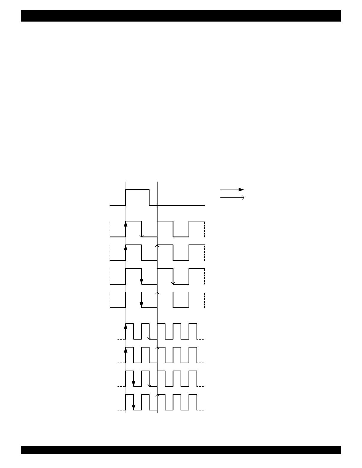
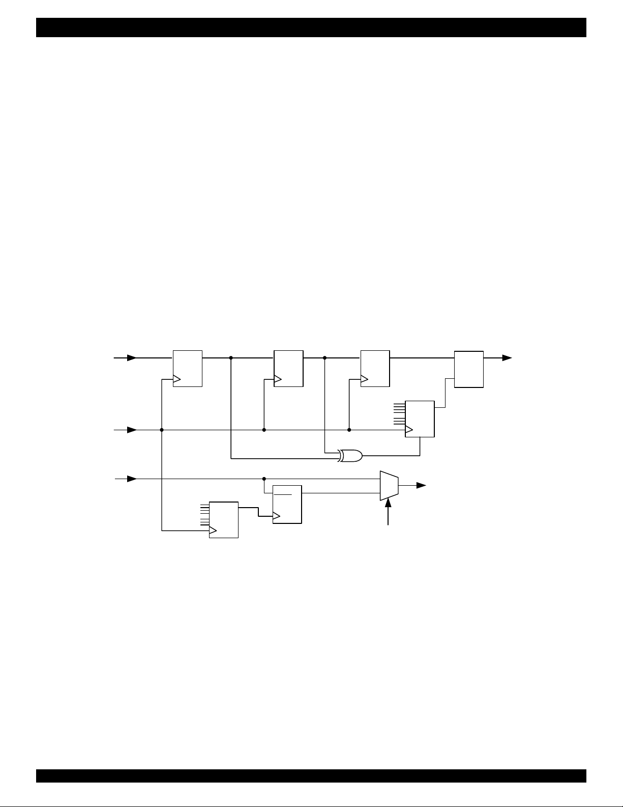
2.6 DEBOUNCE FILTERS
For each channel, the IDT82V1054A provides two debounce filter
circuits: Debounced Switch Hook (DSH) Filter for the SI1 signal and
Ground Key (GK) Filter for the SI2 signal. See Figure - 5 for details. The
two debounce filters are used to buffer the input signals on SI1 and SI2
pins before changing the state of the SLIC Debounced Input SI1/SI2
Register (GREG9). The Frame Sync (FS) signal is necessary for both
DSH and GK filters.
The DSH[3:0] bits in LREG3 are used to program the debounce
period of the SI1 input of the corresponding channel. The DSH filter is
initially clocked at half of the frame sync rate (250
µs). Any data
changing at this sample rate resets a counter that clocks at the rate of 2
ms. The value of the counter is programmable from 0 to 30 via LREG3.
The debounced SI1 signals of Channel 4 to 1 are written to the SIA[3:0]
bits in GREG9. The corresponding SIA bit will not be updated until the
value of the counter is reached. The SI1 pin usually contains the SLIC
switch hook status.
The GK[3:0] bits in LREG3 are used to program the debounce
interval of the SI2 input of the corresponding channel. The debounced
SI2 signals of Channel 4 to 1 are written to the SIB[3:0] bits in GREG9.
The GK debounce filter consists of a six-state up/down counter that
ranges between 0 and 6. This counter is clocked by the GK timer at the
sampling period of 0-30 ms, which is programmed via LREG3. If the
sampled value is low, the value of the counter will be decremented by
each clock pulse. If the sampled value is high, the value of the counter is
incremented by each clock pulse. When the value increases to 6, it sets
a latch whose output is routed to the corresponding SIB bit. If the value
decreases to 0, the latch will be cleared and the output bit will be set to
0. In other cases, the latch and the SIB status remain in their previous
state without being changed. In this way, at least six consecutive GK
clocks with the debounce input remaining at the same state can effect
an output change.
SI1
FS/2
4 kHz
SI2
DQ DQ DQ DQ
GK[3:0]
Debounce
Interval
(0-30 ms)
DQ
7 bit Debounce
Counter
up/
down
6 states
Up/down
Counter
Figure - 5 Debounce Filter
2.7 CHOPPER CLOCK
The IDT82V1054A provides two programmable chopper clock
outputs CHCLK1 and CHCLK2. They can be used to drive the power
supply switching regulators on SLICs. The two chopper clocks are
synchronous to MCLK. The CHCLK1 outputs a signal which clock cycle
is programmable from 2 to 28 ms. The CHCLK2 outputs a signal which
frequency can be 256 kHz, 512 kHz or 16.384 MHz. The frequencies of
the two chopper clocks are programmed by global register GREG5.
2.8 DUAL TONE AND RING GENERATION
The IDT82V1054A provides two tone generators (tone generator 0
SIA
E
DSH[3:0]
Debounce
Period
(0-30 ms)
Q
= 0
≠ 0
GK
DQ
7 bit Debounce
RST
SIB
Counter
and tone generator 1) for each channel. They can produce signals such
as test tone, DTMF, dial tone, busy tone, congestion tone and Caller-ID
Alerting Tone, and output it to the VOUT pin.
The dual tone generators of each channel can be enabled by setting
the TEN0 and TEN1 bits in LREG10 to ‘1’respectively.
The frequency and amplitude of the tone signal are programmed by
the Coe-RAM. The frequency and amplitude coefficients are calculated
by the following formulas:
Frequency coefficient = 32767∗ cos(f / 8000 ∗ 2 ∗ π)
Amplitude coefficient = A ∗ 32767 ∗ sin(f / 8000 ∗ 2 ∗ π)
Herein, 'f' is the desired frequency of the tone signal, 'A' is the scaling
parameter of the amplitude. The range of 'A' is from 0 to 1.
A = 1, corresponds to the maximum amplitude of 1.57 V.
13

IDT82V1054A QUAD PROGRAMMABLE PCM CODEC WITH MPI INTERFACE INDUSTRIAL TEMPERATURE
A = 0, corresponds to the minimum amplitude of 0 V.
It is a linear relationship between 'A' and the amplitude. That is, if
A=β ( 0<β<1), the amplitude will be 1.57 ∗ β (V).
The frequency range is from 25 Hz to 3400 Hz. The frequency
tolerances are as the following:
25 Hz < f < 40 Hz, tolerance < ±12%
40 Hz < f < 60 Hz, tolerance < ±5%
60 Hz < f < 100 Hz, tolerance < ±2.5%
100 Hz < f < 3400 Hz, tolerance < ±1%
The frequency and amplitude coefficients should be converted to
corresponding hexadecimal values before being written to the CoeRAM. Refer to “9 Appendix: IDT82V1054A Coe-RAM Mapping” for the
address of the tone coefficients.
The ring signal is a special signal generated by the dual tone
generators. When only one tone generator is enabled, or dual tone
generators produce the same tone signal and frequency of the tone
meets the ring signal requirement (10 Hz to 100 Hz), a ring signal will be
generated and output to the VOUT pin.
2.9 LEVEL METERING
The IDT82V1054A integrates a level meter which is shared by all 4
channels. The level meter is designed to emulate the off-chip PCM test
equipment so as to facilitate the line-card, subscriber line and users
telephone set monitoring. The level meter tests the return signal and
reports the measurement result via the MPI interface. When combined
with tone generation and loopbacks, it allows the microprocessor to test
the channel integrity. The signal on the channel selected by the CS[1:0]
bits in GREG21 will be metered.
The level meter is enabled by setting the LMO bit in GREG21 to ‘1’. A
level meter counter register (GREG20) is used to set the value of time
cycles for sampling the PCM data (8 kHz sampling rate). The output of
level meter is sent to the level meter result registers GREG18 and
GREG19. The LVLL[7:0] bits in GREG18 contain the lower 7 bits of the
result and a data-ready bit (LVLL[0]), while the LVLH[7:0] bits in
GREG19 contain the higher 8 bits of the result. An internal accumulator
sums the rectified samples until the value set in GREG20 is reached. By
then, the LVLL[0] bit is set to ‘1’ and accumulation result is latched into
GREG18 and GREG19 simultaneously.
Once the higher byte of result (GREG19) is read, the LVLL[0] bit in
GREG18 will be reset. It will be set to ‘1’ again by a new data available.
The contents of GREG18 and GREG19 will be overwritten by the
following metering result if they have not been read out yet. To read the
level meter result registers, it is recommended to read GREG18 (lower
byte of result) first.
The L/C bit in GREG21 determines the level meter operation mode. If
the L/C bit is ‘1’, it means that metering mode is selected. In this mode,
the linear PCM data will be sent to the level meter and the metering
result will be output to GREG18 and GREG19. With this result, the
signal level can be calculated.
For A-law compressed PCM code or linear PCM code, the signal
level can be calculated by the following formula:
LM
A dbm0
()20
log× 3.14+=
For
µ-law compressed PCM code, the signal level can be calculated
Result
--------------------------------------------------------------
LM
Countnumber
25π××
28192××
by the following formula:
LM
()20
A dbm0
log× 3.17+=
LM
: the value in the level meter result registers (GREG18
Result
Result
--------------------------------------------------------------
LM
Countnumber
25π××
28192××
& GREG19);
LM
Countnumber
:the count number of the level meter (set in GREG20).
If the L/C bit is ‘0’, it means that message mode is selected. In this
mode, the compressed PCM data will be output to GREG19
transparently without metering.
Refer to the Application Note for further details on the level meter.
2.10 CHANNEL POWER DOWN/STANDBY MODE
Each individual channel of the IDT82V1054A can be powered down
independently by setting the PD bit in LREG9 to ‘1’. If one channel is
powered down and enters the standby mode, the PCM data transfer and
the D/A, A/D converters of this channel will be disabled. In this way, the
power consumption of the device can be reduced.
When the IDT82V1054A is powered up or reset, all four channels will
be powered down. All circuits that contain programmed information
retain their data after power down. The microprocessor interface is
always active so that new commands can be received and executed.
2.11 POWER DOWN/SUSPEND MODE
A suspend mode is provided for the whole chip to save power. The
suspend mode saves much more power consumption than the standby
mode. In this mode, the PLL block is turned off and the DSP operation is
disabled. Only global and local commands can be executed, the RAM
operation is disabled as the internal clock has been turned off. The PLL
block is powered down by setting the PPD bit in GREG22 to ‘1’. Once
the PLL and all four channels are powered down, the IDT82V1054A will
enter the suspend mode.
14

IDT82V1054A QUAD PROGRAMMABLE PCM CODEC WITH MPI INTERFACE INDUSTRIAL TEMPERATURE
3 OPERATING THE IDT82V1054A
3.1 PROGRAMMING DESCRIPTION
The IDT82V1054A is programmed by writing commands to registers
and coefficient RAM. A Channel Program Enable register (GREG6) is
provided for addressing individual or multiple channels. The CE[3:0] bits
in this register are assigned to Channel 4 to Channel 1 respectively. The
channels are enabled to be programmed by setting their respective CE
bits to ‘1’. If two or more channels are enabled, the successive write
commands will be effective to all enabled channels. A broadcast mode
can be implemented by simply enabling all four channels before
performing other write-operation. The broadcast mode is very useful for
configuring the coefficient RAM of the IDT82V1054A in a large system.
But for read operations, multiple addressing is not allowed.
The IDT82V1054A uses an Identification Code to distinguish itself
from other devices in the system. When being read, the IDT82V1054A
will output an Identification Code of 81H first to indicate that the following
data bytes are from the IDT82V1054A.
3.1.1 COMMAND TYPE AND FORMAT
The IDT82V1054A provides three types of commands as follows:
Local Command (LC), which is used to address the local registers of
the specified channel(s).
Global Command (GC), which is used to address the global registers
of all four channels.
RAM Command (RC), which is used to address the coefficient RAM
(Coe-RAM).
The format of the command is as the following:
b7 b6 b5 b4 b3 b2 b1 b0
R/W CT Address
R/W: Read/Write Command bit
b7 = 0: Read Command
b7 = 1: Write Command
CT: Command Type
b6 b5 = 00: LC - Local Command
b6 b5 = 01: GC - Global Command
b6 b5 = 10: Not Allowed
b6 b5 = 11: RC - RAM Command
Address: b[4:0], specify one or more local/global registers or a block
of Coe-RAM to be addressed.
For Local Command and Global Command, the b[4:0] bits are used
to specify the address of the local registers and global registers
respectively.
For RAM Command, b[4:0] bits are used to specify the block of the
Coe-RAM.
3.1.2 ADDRESSING THE LOCAL REGISTERS
When addressing the local registers, users must specify which
channel(s) will be addressed first. If two or more channels are specified
via GREG6, the corresponding local registers of the specified channels
will be addressed by a Local Command at the same time.
The IDT82V1054A provides a consecutive adjacent addressing
method for accessing the local registers. According to the address
specified in a Local Command, there will be 1 to 4 adjacent local
registers to be addressed automatically, with the highest order first. For
example, if the address specified in a Local Command ends with ‘11’
(b1b0 = 11), 4 adjacent registers will be addressed by this command; if
b1b0 = 10, 3 adjacent registers will be addressed. See Table - 1 for
details.
Table - 1 Consecutive Adjacent Addressing
Address Specified in a Local
Command
b[4:0] = XXX11
(b1b0 = 11, four bytes of data)
b[4:0] = XXX10
(b1b0 = 10, three bytes of data)
b[4:0] = XXX01
(b1b0 = 01, two bytes of data)
b[4:0] = XXX00
(b1b0 = 00, one byte of data)
In/Out Data
Bytes
byte 1 XXX11
byte 2 XXX10
byte 3 XXX01
byte 4 XXX00
byte 1 XXX10
byte 2 XXX01
byte 3 XXX00
byte 1 XXX01
byte 2 XXX00
byte 1 XXX00
Address of the Local
Registers to be accessed
When addressing local registers, the procedure of consecutive
adjacent addressing can be stopped by the CS signal at any time. If CS
is changed from low to high, the operation to the current register and the
next adjacent registers will be aborted. However, the previous operation
results will not be affected.
3.1.3 ADDRESSING THE GLOBAL REGISTERS
For global registers are shared by all four channels, it is no need to
specify the channel(s) before addressing a global register. Except for
this, the global registers are addressed in a similar way as local
registers. The procedure of consecutive adjacent addressing can be
stopped by the CS signal at any time.
3.1.4 ADDRESSING THE COE-RAM
There are totally 40 words of Coe-RAM. They are divided to 5
blocks. Each block consists of 8 words. Each word is 14-bit wide.
The 5 blocks of the Coe-RAM are assigned for different filter
coefficients as shown below (refer to “9 Appendix: IDT82V1054A Coe-
RAM Mapping” for the address of the Coe-RAM):
Block 1: IMF RAM (Word 0 - Word 7), containing the Impedance
Matching Filter coefficient.
Block 2: ECF RAM (Word 8 - Word 15), containing the Echo
Cancellation Filter coefficient.
Block 3: GIS RAM (Word 16 - Word 19) and Tone Generator RAM
(Word 20 - Word 23), containing the Gain of Impedance Scaling and
dual tone coefficients.
Block 4: FRX RAM (Word 24 - Word 30) and GTX RAM (Word 31),
containing the coefficient of the Frequency Response Correction in
Transmit Path and the Gain in Transmit Path;
Block 5: FRR RAM (Word 32 - Word 38) and GRX RAM (Word 39),
containing the coefficient of the Frequency Response Correction in
Receive Path and the Gain in Receive Path.
The Coe-RAM blocks used for containing the IMF, ECF, GIS, FRX,
GTX, FRR and GRX coefficients are shared by all four channels. When
coefficients are written to these blocks, they will be used by all four
channels. But the four words (word 20 to 23), which contain the dual
15

IDT82V1054A QUAD PROGRAMMABLE PCM CODEC WITH MPI INTERFACE INDUSTRIAL TEMPERATURE
tone coefficients, can only be addressed on a per-channel basis.
Therefore, users should specify a channel (by setting the corresponding
CE bit in GREG6 to ‘1’) before writing/reading tone coefficients to/from
the Coe-RAM.
To write a Coe-RAM word, 16 bits (b[15:0]) or two 8-bit bytes are
needed to fulfill with MSB first, but the lowest two bits (b[1:0]) will be
ignored. When read, each word will output 16 bits with MSB first, but the
lowest two bits (b[1:0]) are meaningless.
The address in a Coe-RAM command (b[4:0]) specifies a block of
Coe-RAM to be accessed. When a Coe-RAM command is executed, the
CODEC automatically counts down from the highest address to the
lowest address of the specified block. So all 8 words of the block will be
addressed by one Coe-RAM command.
When addressing the Coe-RAM, the procedure of consecutive
adjacent addressing can be stopped by the CS signal at any time. If the
CS signal is changed from low to high, the operation to the current word
and the next adjacent words will be aborted. However, the previous
operation results will not be affected.
3.1.5 PROGRAMMING EXAMPLES
3.1.5.1 Example of Programming Local Registers
• Writing to LREG2 and LREG1 of Channel 1:
1010, 0101 Channel Enable command
0001, 0010 Data for GREG6 (Channel 1 is enabled for programming)
1000, 0001 Local register write command (The address is '00001', which means that data will be written to LREG2 and LREG1.)
xxxx, xxxx Data for LREG2
xxxx, xxxx Data for LREG1
• Reading from LREG2 and LREG1 of Channel 1:
1010, 0101 Channel Enable command
0001, 0010 Data for GREG6 (Channel 1 is enabled for programming)
0000, 0001 Local register read command (The address is '00001', which means that LREG2 and LREG1 will be read.)
After the preceding commands are executed, data will be sent out as follows:
1000, 0001 Identification code
xxxx, xxxx Data read out from LREG2
xxxx, xxxx Data read out from LREG1
3.1.5.2 Example of Programming Global Registers
• Writing to GREG1:
1010, 0000 Global register write command (The address is '00000', which means that data will be written to GREG1.)
1111, 1111 Data f or GREG1
• Reading from GREG1:
0010, 0000 Global register read command (The address is '00000', which means that GREG1 will be read.)
After the preceding command is executed, data will be sent out as follows:
1000, 0001 Identification code
0000, 0001 Data read out from GREG1
3.1.5.3 Example of Programming the Coefficient-RAM
As described in “3.1.4 Addressing the Coe-RAM”, the Coe-RAM blocks used for containing the IMF, ECF, GIS, FRX, GTX, FRR and GRX
coefficients are shared by all four channels. When coefficients are written to these blocks, they will be used by all four channels. But the four words
(word 20 to 23), which contain the tone coefficients, can only be addressed on a per-channel basis. Therefore, users should specify a channel before
writing/reading tone coefficients to/from the Coe-RAM.
• Writing to the Coe-RAM
− Examples for Coe-RAM blocks shared by all four channels:
1110,0000 Coe-RAM write command (The address of '00000' is located in block 1, which means that data will be written to block 1.)
data byte 1 high byte of word 8 of block 1
data byte 2 low byte of word 8 of block 1
data byte 3 high byte of word 7 of block 1
data byte 4 low byte of word 7 of block 1
data byte 5 high byte of word 6 of block 1
data byte 6 low byte of word 6 of block 1
data byte 7 high byte of word 5 of block 1
data byte 8 low byte of word 5 of block 1
data byte 9 high byte of word 4 of block 1
data byte 10 low byte of word 4 of block 1
data byte 11 high byte of word 3 of block 1
data byte 12 low byte of word 3 of block 1
data byte 13 high byte of word 2 of block 1
16

IDT82V1054A QUAD PROGRAMMABLE PCM CODEC WITH MPI INTERFACE INDUSTRIAL TEMPERATURE
data byte 14 low byte of word 2 of block 1
data byte 15 high byte of word 1 of block 1
data byte 16 low byte of word 1 of block 1
− Examples for the Coe-RAM used for tone coefficients:
1010,0101 Channel Enable command
0001,0010 Data for GREG6 (Channel 1 is enabled for programming)
1110,0010 Coe-RAM write command (The address of '00010' is located in block 3, which means that data will be written to block 3.)
data byte 1 high byte of word 8 of block 3
data byte 2 low byte of word 8 of block 3
data byte 3 high byte of word 7 of block 3
data byte 4 low byte of word 7 of block 3
data byte 5 high byte of word 6 of block 3
data byte 6 low byte of word 6 of block 3
data byte 7 high byte of word 5 of block 3
data byte 8 low byte of word 5 of block 3
data byte 9 high byte of word 4 of block 3 (see Note 1)
data byte 10 low byte of word 4 of block 3
data byte 11 high byte of word 3 of block 3
data byte 12 low byte of word 3 of block 3
data byte 13 high byte of word 2 of block 3
data byte 14 low byte of word 2 of block 3
data byte 15 high byte of word 1 of block 3
data byte 16 low byte of word 1 of block 3
Note 1: In block 3 of the Coe-RAM, word 5 to word 8 are used for tone coefficients while word 1 to word 4 are used for GIS coefficients. If users do not want to change the GIS coefficient
while writing tone coefficients to the Coe-RAM, they can stop the procedure of consecutive adjacent addressing (after writing data to word 5) by pulling the CS signal to high, or they can
rewrite word 1 to word 4 with the original GIS coefficients.
• Reading from the Coe-RAM
− Examples for Coe-RAM blocks shared by all four channels:
0110,0000 Coe-RAM read command (The address of '00000' is located in block 1, which means that block 1 will be read.)
After the preceding command is executed, data will be sent out as follows:
1000,0001 Identification code
data byte 1 data read out from high byte of word 8 of block 1
data byte 2 data read out from low byte of word 8 of block 1
data byte 3 data read out from high byte of word 7 of block 1
data byte 4 data read out from low byte of word 7 of block 1
data byte 5 data read out from high byte of word 6 of block 1
data byte 6 data read out from low byte of word 6 of block 1
data byte 7 data read out from high byte of word 5 of block 1
data byte 8 data read out from low byte of word 5 of block 1
data byte 9 data read out from high byte of word 4 of block 1
data byte 10 data read out from low byte of word 4 of block 1
data byte 11 data read out from high byte of word 3 of block 1
data byte 12 data read out from low byte of word 3 of block 1
data byte 13 data read out from high byte of word 2 of block 1
data byte 14 data read out from low byte of word 2 of block 1
data byte 15 data read out from high byte of word 1 of block 1
data byte 16 data read out from low byte of word 1 of block 1
− Examples for the Coe-RAM used for tone coefficients:
1010,0011 Channel Enable command
0001,0010 Data for GREG6 (Channel 1 is enabled for programming)
0110,0010 Coe-RAM read command (The address of '00010' is located in block 3, which means that block 3 will be read.)
After the preceding commands are executed, data will be sent out as follows:
1000,0001 Identification code
data byte 1 data read out from high byte of word 8 of block 3
data byte 2 data read out from low byte of word 8 of block 3
data byte 3 data read out from high byte of word 7 of block 3
17

IDT82V1054A QUAD PROGRAMMABLE PCM CODEC WITH MPI INTERFACE INDUSTRIAL TEMPERATURE
data byte 4 data read out from low byte of word 7 of block 3
data byte 5 data read out from high byte of word 6 of block 3
data byte 6 data read out from low byte of word 6 of block 3
data byte 7 data read out from high byte of word 5 of block 3
data byte 8 data read out from low byte of word 5 of block 3
data byte 9 data read out from high byte of word 4 of block 3
data byte 10 data read out from low byte of word 4 of block 3
data byte 11 data read out from high byte of word 3 of block 3
data byte 12 data read out from low byte of word 3 of block 3
data byte 13 data read out from high byte of word 2 of block 3
data byte 14 data read out from low byte of word 2 of block 3
data byte 15 data read out from high byte of word 1 of block 3
data byte 16 data read out from low byte of word 1 of block 3
18

IDT82V1054A QUAD PROGRAMMABLE PCM CODEC WITH MPI INTERFACE INDUSTRIAL TEMPERATURE
3.2 POWER-ON SEQUENCE
To power on the IDT82V1054A, users should follow the sequence
below:
1. Apply ground first;
2. Apply VCC, finish signal connections and set the RESET pin to logic
low. The device then goes into the default state;
3. Set the RESET pin to logic high;
4. Select master clock frequency;
5. Program filter coefficients and other parameters as required;
3.3 DEFAULT STATE AFTER RESET
When the IDT82V1054A is powered on, or reset either by command
or by setting the RESET pin to logic low for at least 50
enter the default state as follows:
1. All four channels are powered down and in standby mode.
2. All loopbacks and cutoff are disabled.
3. The DX1 pin is selected for all channels to transmit data and the DR1
pin is selected for all channels to receive data.
µs, the device will
4. The master clock frequency is 2.048 MHz.
5. Transmit and receive time slots are set to be 0-3 respectively for
Channel 1-4. The PCM data rate is as same as the BCLK frequency.
The PCM data is transmitted on rising edges of the BCLK signal and
received on falling edges of it.
6. A-Law is selected.
7. The digital filters including GRX, FRR, GTX, FRX, GIS, ECF and IMF
are disabled. The high-pass filters (HPF) are enabled. Refer to
Figure - 4 and descriptions on LREG1 for details.
8. The SB1, SB2 and SB3 pins are configured as inputs.
9. The SI1 and SI2 pins are configured as no debounce.
10.All interrupts are disabled and all pending interrupts are cleared.
11.All feature function blocks including dual tone generators, hardware
ring trip and level meter are disabled.
12.The outputs of CHCLK1 and CHCLK2 are set to high.
The data stored in the RAM will not be changed by any kind of reset
operations. So the RAM data will not be lost unless the device is
powered down physically.
19

IDT82V1054A QUAD PROGRAMMABLE PCM CODEC WITH MPI INTERFACE INDUSTRIAL TEMPERATURE
3.4 REGISTERS DESCRIPTION
3.4.1 REGISTERS OVERVIEW
Table - 2 Global Registers (GREG) Mapping
Name Function
GREG1
GREG2
GREG3 Software reset − A2H −
GREG4
GREG5
GREG6
GREG7
GREG8
GREG9
GREG10
GREG11
GREG12
GREG13
GREG14 Reserved for future use Reserved −−−
GREG15
GREG16
GREG17 Reserved for future use Reserved −−−
GREG18
GREG19
GREG20
GREG21
GREG22
Version number (read)/
no operation (write)
Interrupt clear − A1H −
Hardware reset − A3H −
Chopper clock
selection
MCLK selection and
channel program
enable
Data format,
companding law, clock
slope and PCM delay
time selection
SLIC ring trip setting
and control
Debounced data on
SI1 and SI2 pins
SB1 direction control
and SB1 data
SB2 direction control
and SB2 data
SB3 direction control
and SB3 data
Reserved for future use Reserved −−−
Reserved for future use Reserved −−−
Reserved for future use Reserved −−−
Level meter result low
byte
Level meter result high
byte
Level meter count
number
level meter mode and
channel selection, level
meter enable
Loopback control and
PLL power down
b7 b6 b5 b4 b3 b2 b1 b0
Reserved CHclk2[1] CHclk2[0] CHclk1[3] CHclk1[2] CHclk1[1] CHclk1[0] 24H A4H 00H
CE[3] CE[2] CE[1] CE[0] Sel[3] Sel[2] Sel[1] Sel[0] 25H A5H 02H
A-µ VDS CS[2] CS[1] CS[0] OC[2] OC[1] OC[0] 26H A6H 00H
OPI Reserved IPI IS RTE OS[2] OS[1] OS[0] 27H A7H 00H
SIB[3] SIB[2] SIB[1] SIB[0] SIA[3] SIA[2] SIA[1] SIA[0] 28H − 00H
SB1C[3] SB1C[2] SB1C[1] SB1C[0] SB1[3] SB1[2] SB1[1] SB1[0] 29H A9H 00H
SB2C[3] SB2C[2] SB2C[1] SB2C[0] SB2[3] SB2[2] SB2[1] SB2[0] 2AH AAH 00H
SB3C[3] SB3C[2] SB3C[1] SB3C[0] SB3[3] SB3[2] SB3[1] SB3[0] 2BH ABH 00H
LVL L[7] LV LL[ 6] LVL L[ 5] LV LL [4] LVLL[ 3] LV LL[2 ] LVLL [1] LVLL[0] 31H − 00H
LVL H[7] LVL H[ 6] LV LH[ 5] LV LH[ 4] LV LH[3 ] LV LH [2] LV LH[1 ] LVLH[0] 32H − 00H
CN[7] CN[6] CN[5] CN[4] CN[3] CN[2] CN[1] CN[0] 33H B3H 00H
Reserved LMO L/C CS[1] CS[0] 34H B4H 00H
Reserved PPD DLB_ANA ALB_8k DLB_8k DLB_DI ALB_DI 35H B5H 00H
Register Byte
Read
Command
20H A0H 01H
Write
Command
Default
Value
20

IDT82V1054A QUAD PROGRAMMABLE PCM CODEC WITH MPI INTERFACE INDUSTRIAL TEMPERATURE
Table - 3 Local Registers (LREG) Mapping
Register Byte Read
Name Function
LREG1 Coefficient selection CS[7] CS[6] CS[5] CS[4] CS[3] CS[2] CS[1] CS[0] 00H 80H 08H
Local loopbacks
LREG2
LREG3
LREG4
LREG5
LREG6
LREG7
LREG8 PCM data high byte PCM[15] PCM[14] PCM[13] PCM[12] PCM[11] PCM[10] PCM[9] PCM[8] 07H − 00H
LREG9
LREG1
control and SLIC input
interrupt enable
DSH and GK
debounce filters
configuration
SLIC IO status/control
data
Transmit highway and
time slot selection
Receive highway and
time slot selection
PCM data low byte PCM[7] PCM[6] PCM[5] PCM[4] PCM[3] PCM[2] PCM[1] PCM[0] 06H − 00H
Channel power down,
A/D and D/A gains,
PCM cutoff
Tone generator
enable and tone
0
program enable
b7 b6 b5 b4 b3 b2 b1 b0
IE[4] IE[3] IE[2] IE[1] IE[0] DLB_PCM ALB_1BIT DLB_1BIT 01H 81H 00H
GK[3] GK[2] GK[1] GK[0] DSH[3] DSH[2] DSH[1] DSH[0] 02H 82H 00H
Reserved SO2 SO1 SB3 SB2 SB1 SI2 SI1 03H 83H −
THS TT[6] TT[5] TT[4] TT[3] TT[2] TT[1] TT[0] 04H 84H
RHS RT[6] RT[5] RT[4] RT[3] RT[2] RT[1] RT[0] 05H 85H
PD PCMCT GAD GDA 0 0 0 0 08H 88H 80H
Reserved TPROG1 TPROG0 TEN1 TEN0 09H 89H 00H
Comman
d
Write
Comman
d
Default
Value
00H for CH1
01H for CH2
02H for CH3
03H for CH4
00H for CH1
01H for CH2
02H for CH3
03H for CH4
21

IDT82V1054A QUAD PROGRAMMABLE PCM CODEC WITH MPI INTERFACE INDUSTRIAL TEMPERATURE
For the global and local registers described below, it should be noted that:
1. R/W = 0, Read command. R/W = 1, Write command.
2. The reserved bit(s) in the registers must be filled in ‘0’ in write operation and be ignored in read operation.
3.4.2 GLOBAL REGISTERS LIST
GREG1: No Operation, Write (A0H); Version Number, Read (20H)
b7 b6 b5 b4 b3 b2 b1 b0
Command R/W0100000
By applying a read operation (20H) to this register, users can read out the version number of the IDT82V1054A. The default value is 01H.
To write to this register (no operation), a data byte of FFH must follow the write command (A0H) to ensure proper operation.
GREG2: Interrupt Clear, Write Only (A1H)
b7 b6 b5 b4 b3 b2 b1 b0
Command10100001
All interrupts on SLIC I/O will be cleared by applying a write operation to this register. Note that a data byte of FFH must follow the write
command (A1H) to ensure proper operation.
GREG3: Software Reset, Write Only (A2H)
b7 b6 b5 b4 b3 b2 b1 b0
Command10100010
A write operation to this register resets all local registers, but does not reset global registers and the Coe-RAM. Note that when writing to
this register, a data byte of FFH must follow the write command (A2H) to ensure proper operation.
GREG4: Hardware Reset, Write Only (A3)
b7 b6 b5 b4 b3 b2 b1 b0
Command10100011
A write operation to this register is equivalent to setting the RESET pin to logic low (Refer to “3.3 Default State After Reset” on page 19
for details). Note that when applying this write command, a data byte of FFH must follow to ensure proper operation.
GREG5: Chopper Clock Selection, Read/Write (24H/A4H)
b7 b6 b5 b4 b3 b2 b1 b0
Command R/W0100100
I/O data Reserved Chclk2[1] Chclk2[0] Chclk1[3] Chclk1[2] Chclk1[1] Chclk1[0]
This register is used to select the frequency of the CHclk2 and CHclk1 output signals.
CHclk2[1:0] = 00: the output of chclk2 is set to high permanently (default);
CHclk2[1:0] = 01: chclk2 outputs a digital signal with the frequency of 512 kHz;
CHclk2[1:0] = 10: chclk2 outputs a digital signal with the frequency of 256 kHz;
CHclk2[1:0] = 11: chclk2 outputs a digital signal with the frequency of 16384 kHz;
CHclk1[3:0] = 0000: the output of chclk1 is set to high permanently (default);
CHclk1[3:0] = 0001: chclk1 outputs a digital signal with the frequency of 1000/2 Hz;
CHclk1[3:0] = 0010: chclk1 outputs a digital signal with the frequency of 1000/4 Hz;
CHclk1[3:0] = 0011: chclk1 outputs a digital signal with the frequency of 1000/6 Hz;
CHclk1[3:0] = 0100: chclk1 outputs a digital signal with the frequency of 1000/8 Hz;
CHclk1[3:0] = 0101: chclk1 outputs a digital signal with the frequency of 1000/10 Hz;
CHclk1[3:0] = 0110: chclk1 outputs a digital signal with the frequency of 1000/12 Hz;
CHclk1[3:0] = 0111: chclk1 outputs a digital signal with the frequency of 1000/14 Hz;
CHclk1[3:0] = 1000: chclk1 outputs a digital signal with the frequency of 1000/16 Hz;
22

IDT82V1054A QUAD PROGRAMMABLE PCM CODEC WITH MPI INTERFACE INDUSTRIAL TEMPERATURE
CHclk1[3:0] = 1001: chclk1 outputs a digital signal with the frequency of 1000/18 Hz;
CHclk1[3:0] = 1010: chclk1 outputs a digital signal with the frequency of 1000/20 Hz;
CHclk1[3:0] = 1011: chclk1 outputs a digital signal with the frequency of 1000/22 Hz;
CHclk1[3:0] = 1100: chclk1 outputs a digital signal with the frequency of 1000/24 Hz;
CHclk1[3:0] = 1101: chclk1 outputs a digital signal with the frequency of 1000/26 Hz;
CHclk1[3:0] = 1110: chclk1 outputs a digital signal with the frequency of 1000/28 Hz;
CHclk1[3:0] = 1111: the output of chclk1 is set to low permanently.
GREG6: MCLK Selection and Channel Program Enable, Read/Write (25H/A5H)
b7 b6 b5 b4 b3 b2 b1 b0
Command R/W0100101
I/O data CE[3] CE[2] CE[1] CE[0] Sel[3] Sel[2] Sel[1] Sel[0]
The higher 4 bits (CE[3:0]) in this register are used to specify the desired channel(s) before addressing local registers or Coe-RAM used
for tone coefficients. The CE[0] to CE[3] bits indicate the program enable state for Channel 1 to Channel 4 respectively.
CE[0] = 0: Disabled, Channel 1 can not receive programming commands (default);
CE[0] = 1: Enabled, Channel 1 can receive programming commands;
CE[1] = 0: Disabled, Channel 2 can not receive programming commands (default);
CE[1] = 1: Enabled, Channel 2 can receive programming commands;
CE[2] = 0: Disabled, Channel 3 can not receive programming commands (default);
CE[2] = 1: Enabled, Channel 3 can receive programming commands;
CE[3] = 0: Disabled, Channel 4 can not receive programming commands (default);
CE[3] = 1: Enabled, Channel 4 can receive programming commands.
The lower 4 bits (Sel[3:0]) in this register are used to select the Master Clock frequency.
Sel[3:0] = 0000: 8.192 MHz
Sel[3:0] = 0001: 4.096 MHz
Sel[3:0] = 0010: 2.048 MHz (default)
Sel[3:0] = 0110: 1.536 MHz
Sel[3:0] = 1110: 1.544 MHz
Sel[3:0] = 0101: 3.072 MHz
Sel[3:0] = 1101: 3.088 MHz
Sel[3:0] = 0100: 6.144 MHz
Sel[3:0] = 1100: 6.176 MHz
GREG7: A/
The A/
AA-
The Voice Data Select bit (VDS) defines the format of the voice data:
VDS = 0: Compressed code (default)
VDS = 1: Linear code
µ-law, Linear/Compressed Code, Clock Slope and Delay Time Selection, Read/Write (26H/A6H)
b7 b6 b5 b4 b3 b2 b1 b0
Command R/W0100110
I/O data A-µ VDS CS[2] CS[1] CS[0] OC[2] OC[1] OC[0]
µ-law select bit (A-µ) selects the companding law:
µ = 0: A-law is selected (default)
µ = 1: µ-law is selected.
The Clock Slope bits (CS[2:0]) select single or double clock and clock edges of transmitting and receiving data.
CS[2] = 0: Single clock (default)
CS[2] = 1: Double clock
CS[1:0] = 00: transmits data on rising edges of BCLK, receives data on falling edges of BCLK (default).
CS[1:0] = 01: transmits data on rising edges of BCLK, receives data on rising edges of BCLK.
CS[1:0] = 10: transmits data on falling edges of BCLK, receives data on falling edges of BCLK.
CS[1:0] = 11: transmits data on falling edges of BCLK, receives data on rising edges of BCLK.
23

IDT82V1054A QUAD PROGRAMMABLE PCM CODEC WITH MPI INTERFACE INDUSTRIAL TEMPERATURE
The PCM data Offset Configuration bits (OC[2:0]) determine that the transmit and receive time slots of PCM data offset from the FS
signal by how many periods of BCLK:
OC[2:0] = 000: 0 period of BCLK (default);
OC[2:0] = 001: 1 period of BCLK;
OC[2:0] = 010: 2 periods of BCLK;
OC[2:0] = 011: 3 periods of BCLK;
OC[2:0] = 100: 4 periods of BCLK;
OC[2:0] = 101: 5 periods of BCLK;
OC[2:0] = 110: 6 periods of BCLK;
OC[2:0] = 111: 7 periods of BCLK.
GREG8: SLIC Ring Trip Setting and Control, Read/Write (27H/A7H)
b7 b6 b5 b4 b3 b2 b1 b0
Command R/W0100111
I/O data OPI Reserved IPI IS RTE OS[2] OS[1] OS[0]
The Output Polarity Indicator bit (OPI) indicates the valid polarity of output:
OPI = 0: the selected output pin changes from high to low to activate the ring (default);
OPI = 1: the selected output pin changes from low to high to activate the ring.
The Input Polarity Indicator bit (IPI) indicates the valid polarity of input:
IPI = 0: active low (default);
IPI = 1: active high.
The Input Selection bit (IS) determines which input will be selected as the off-hook indication signal source.
IS = 0: SI1 is selected (default);
IS = 1: SI2 is selected.
The Ring Trip Enable bit (RTE) enables or disables the ring trip function block:
RTE = 0: the ring trip function block is disabled (default);
RTE = 1: the ring trip function block is enabled.
The Output Selection bits (OS[2:0]) determine which output will be selected as the ring control signal source.
OS[2:0] = 000 - 010: not defined;
OS[2:0] = 011: SB1 is selected (when SB1 is configured as an output);
OS[2:0] = 100: SB2 is selected (when SB2 is configured as an output);
OS[2:0] = 101: SB3 is selected (when SB3 is configured as an output);
OS[2:0] = 110: SO1 is selected;
OS[2:0] = 111: SO2 is selected.
GREG9: SI Data, Read Only (28H)
b7 b6 b5 b4 b3 b2 b1 b0
Command00101000
I/O data SIB[3] SIB[2] SIB[1] SIB[0] SIA[3] SIA[2] SIA[1] SIA[0]
The SIA[3:0] bits contain the debounced data (off-hook status) on the SI1 pins of Channel 4 to Channel 1 respectively.
The SIB[3:0] bits contain the debounced data (ground key status) on the SI2 pins of Channel 4 to Channel 1 respectively.
24

IDT82V1054A QUAD PROGRAMMABLE PCM CODEC WITH MPI INTERFACE INDUSTRIAL TEMPERATURE
GREG10: SB1 Direction Control and SB1 Status/Control Data, Read/Write (29H/A9H)
b7 b6 b5 b4 b3 b2 b1 b0
Command R/W0101001
I/O data SB1C[3] SB1C[2] SB1C[1] SB1C[0] SB1[3] SB1[2] SB1[1] SB1[0]
The SB1 direction control bits SB1C[3:0] in this register determine the directions of the SB1 pins of Channel 4 to Channel 1 respectively.
SB1C[0] = 0: the SB1 pin of Channel 1 is configured as input (default);
SB1C[0] = 1: the SB1 pin of Channel 1 is configured as output;
SB1C[1] = 0: the SB1 pin of Channel 2 is configured as input (default);
SB1C[1] = 1: the SB1 pin of Channel 2 is configured as output;
SB1C[2] = 0: the SB1 pin of Channel 3 is configured as input (default);
SB1C[2] = 1: the SB1 pin of Channel 3 is configured as output;
SB1C[3] = 0: the SB1 pin of Channel 4 is configured as input (default);
SB1C[3] = 1: the SB1 pin of Channel 4 is configured as output.
When the SB1 pins of Channel 1 to Channel 4 are configured as inputs, the SB1[0] to SB1[3] bits contain the status of these four SB1
pins respectively. When the SB1 pins of Channel 1 to Channel 4 are configured as outputs, the control data is written to these four SB1
pins via the SB1[0] to SB1[3] bits respectively.
GREG11: SB2 Direction Control and SB2 Status/Control Data, Read/Write (2AH/AAH)
b7 b6 b5 b4 b3 b2 b1 b0
Command R/W0101010
I/O data SB2C[3] SB2C[2] SB2C[1] SB2C[0] SB2[3] SB2[2] SB2[1] SB2[0]
The SB2 direction control bits SB2C[3:0] in this register determine the directions of the SB2 pins of Channel 4 to Channel 1 respectively.
SB2C[0] = 0: the SB2 pin of Channel 1 is configured as input (default);
SB2C[0] = 1: the SB2 pin of Channel 1 is configured as output;
SB2C[1] = 0: the SB2 pin of Channel 2 is configured as input (default);
SB2C[1] = 1: the SB2 pin of Channel 2 is configured as output;
SB2C[2] = 0: the SB2 pin of Channel 3 is configured as input (default);
SB2C[2] = 1: the SB2 pin of Channel 3 is configured as output;
SB2C[3] = 0: the SB2 pin of Channel 4 is configured as input (default);
SB2C[3] = 1: the SB2 pin of Channel 4 is configured as output.
When the SB2 pins of Channel 1 to Channel 4 are configured as inputs, the SB2[0] to SB2[3] bits contain the status of these four SB2
pins respectively. When the SB2 pins of Channel 1 to Channel 4 are configured as outputs, the control data is written to these four SB2
pins via the SB2[0] to SB2[3] bits respectively.
GREG12: SB3 Direction Control and SB3 Status/Control Data, Read/Write (2BH/ABH)
b7 b6 b5 b4 b3 b2 b1 b0
Command R/W0101011
I/O data SB3C[3] SB3C[2] SB3C[1] SB3C[0] SB3[3] SB3[2] SB3[1] SB3[0]
The SB3 direction control bits SB3C[3:0] in this register determine the directions of the SB3 pins of Channel 4 to Channel 1 respectively.
SB3C[0] = 0: the SB3 pin of Channel 1 is configured as input (default);
SB3C[0] = 1: the SB3 pin of Channel 1 is configured as output;
SB3C[1] = 0: the SB3 pin of Channel 2 is configured as input (default);
SB3C[1] = 1: the SB3 pin of Channel 2 is configured as output;
SB3C[2] = 0: the SB3 pin of Channel 3 is configured as input (default);
SB3C[2] = 1: the SB3 pin of Channel 3 is configured as output;
SB3C[3] = 0: the SB3 pin of Channel 4 is configured as input (default);
SB3C[3] = 1: the SB3 pin of Channel 4 is configured as output.
When the SB3 pins of Channel 1 to Channel 4 are configured as inputs, the SB3[0] to SB3[3] bits contain the status of these four SB3
25

IDT82V1054A QUAD PROGRAMMABLE PCM CODEC WITH MPI INTERFACE INDUSTRIAL TEMPERATURE
pins respectively. When the SB3 pins of Channel 1 to Channel 4 are configured as outputs, the control data is written to these four SB3
pins via the SB3[0] to SB3[3] bits respectively.
GREG13: Reserved for future use.
GREG14: Reserved for future use.
GREG15: Reserved for future use.
GREG16: Reserved for future use.
GREG17: Reserved for future use.
GREG18: Level Meter Result Low Byte, Read Only (31H)
b7 b6 b5 b4 b3 b2 b1 b0
Command00110001
I/O data LVLL[7] LVLL[6] LVLL[5] LVLL[4] LVLL[3] LVLL[2] LVLL[1] LVLL[0]
This register contains the low byte of the level meter result. The default value is 00H.
The LVLL[0] bit in this register will be set to ‘1’ when the level meter result (both high and low bytes) is ready, and it will be reset to ‘0’
immediately after the high byte of result is read. To read the level meter result, it is recommended to the low byte first, then read the high
byte (LVLH[7:0] in GREG19).
GREG19: Level Meter Result High Byte, Read Only (32H)
b7 b6 b5 b4 b3 b2 b1 b0
Command00110010
I/O data LVLH[7] LVLH[6] LVLH[5] LVLH[4] LVLH[3] LVLH[2] LVLH[1] LVLH[0]
This register contains the high byte of the level meter result. The default value is 00H.
GREG20: Level Meter Count Number, Read/Write (33H/B3H)
b7 b6 b5 b4 b3 b2 b1 b0
Command R/W0110011
I/O data CN[7] CN[6] CN[5] CN[4] CN[3] CN[2] CN[1] CN[0]
The CN[7:0] bits are used to set the number of time cycles for sampling the PCM data.
CN[7:0] = 0 (d): the PCM data is output to the result registers GREG18 and GREG19 directly;
CN[7:0] = N (d): the PCM data is sampled for N × 125
µs (N is from 1 to 255).
GREG21: Level Meter Channel and Linear/Compressed Mode Selection, Level Meter On/Off, Read/Write (34H/B4H)
b7 b6 b5 b4 b3 b2 b1 b0
Command R/W0110100
I/O data Reserved LMO L/C CS[1] CS[0]
The Level Meter On/Off bit (LMO) enables/disables the level meter.
LMO = 0: The level meter is disabled (default);
LMO = 1: The level meter is enabled.
The Linear/Compressed bit (L/C) determines the mode of level meter operation.
L/C = 0: Message mode is selected. The compressed PCM data will be output to GREG19 transparently (default).
L/C = 1: Metering mode is selected. The linear PCM data will be metered and the result will be output to the registers
GREG18 and GREG19.
26

IDT82V1054A QUAD PROGRAMMABLE PCM CODEC WITH MPI INTERFACE INDUSTRIAL TEMPERATURE
The Level Meter Channel Select bits (CS[1:0]) select a channel, data on which will be level metered.
CS[1:0] = 00: Channel 1 is selected (default);
CS[1:0] = 01: Channel 2 is selected;
CS[1:0] = 10: Channel 3 is selected;
CS[1:0] = 11: Channel 4 is selected.
GREG22: Global Loopback Control and PLL Power Down, Read/Write (35H/B5H)
b7 b6 b5 b4 b3 b2 b1 b0
Command R/W0110101
I/O data Reserved PPD DLB_ANA ALB_8k DLB_8k DLB_DI ALB_DI
The PLL Power Down bit (PPD) controls the operation state of the PLL block.
PPD = 0: The PLL is disabled. The device is in normal operation state (default);
PPD = 1: The PLL is powered down. The device works in power-saving mode. All clocks stop running.
The Loop Control bits determine the loopback status. Refer to Figure - 4 on page 11 for detailed information.
DLB_ANA = 0: The Digital Loopback via Analog Interface is disabled (default);
DLB_ANA = 1: The Digital Loopback via Analog Interface is enabled.
ALB_8k = 0: The Analog Loopback via 8 kHz Interface is disabled (default);
ALB_8k = 1: The Analog Loopback via 8 kHz Interface is enabled.
DLB_8k = 0: The Digital Loopback via 8 kHz Interface is disabled (default);
DLB_8k = 1: The Digital Loopback via 8 kHz Interface is enabled.
DLB_DI = 0: The Digital Loopback from DR to DX is disabled (default);
DLB_DI = 1: The Digital Loopback from DR to DX is enabled.
ALB_DI = 0: The Analog Loopback from DX to DR is disabled (default);
ALB_DI = 1: The Analog Loopback from DX to DR is enabled.
27

IDT82V1054A QUAD PROGRAMMABLE PCM CODEC WITH MPI INTERFACE INDUSTRIAL TEMPERATURE
3.4.3 LOCAL REGISTERS LIST
LREG1: Coefficient Selection, Read/Write (00H/80H)
b7 b6 b5 b4 b3 b2 b1 b0
Command R/W0000000
I/O data CS[7] CS[6] CS[5] CS[4] CS[3] CS[2] CS[1] CS[0]
The Coefficient Select bits (CS[7:0]) are used to control digital filters and function blocks on each channel. The digital filters include
Impedance Matching Filter, Echo Cancellation Filter, High-Pass Filter, Gain for Impedance Scaling, Gain in the Transmit/Receive Path
and Frequency Response Correction in the Transmit/Receive Path. See Figure - 4 on page 11 for details. It should be noted that the
Impedance Matching Filter and Gain for Impedance Scaling are working together to adjust the impedance. So the CS[0] and CS[2] bits
should be set to the same value to ensure proper operation.
CS[7] = 0: The Digital Gain Filter in the Receive path (GRX) is disabled (default);
CS[7] = 1: The Digital Gain in the Receive path (GRX) is programmed by the Coe-RAM.
CS[6] = 0: The Frequency Response Correction filter in the Receive path (FRR) is disabled (default);
CS[6] = 1: The coefficient of the Frequency Response Correction filter in the Receive path (FRR) is programmed by the Coe-RAM.
CS[5] = 0: The Digital Gain Filter in the Transmit path (GTX) is disabled (default);
CS[5] = 1: The Digital Gain in the Transmit path (GTX) is set by the Coe-RAM.
CS[4] = 0: The Frequency Response Correction filter in the Transmit path (FRX) is disabled (default);
CS[4] = 1: The coefficient of the Frequency Response Correction filter in the Transmit path (FRX) is programmed by the Coe-RAM.
CS[3] = 0: The High-Pass Filter (HPF) is bypassed/disabled;
CS[3] = 1: The High-Pass Filter (HPF) is enabled (default).
CS[2] = 0: The Gain for Impedance Scaling filter (GIS) is disabled (default);
CS[2] = 1: The coefficient of the Gain for Impedance Scaling filter (GIS) is programmed by the Coe-RAM.
CS[1] = 0: The Echo Cancellation Filter (ECF) is disabled (default);
CS[1] = 1: The coefficient of the Echo Cancellation Filter (ECF) is programmed by the Coe-RAM.
CS[0] = 0: The Impedance Matching Filter (IMF) is disabled (default);
CS[0] = 1: The coefficient of the Impedance Matching Filter (IMF) is programmed by the Coe-RAM.
LREG2: Local Loopback Control and SLIC Input Interrupt Enable, Read/Write (01H/81H)
b7 b6 b5 b4 b3 b2 b1 b0
Command R/W0000001
I/O data IE[4] IE[3] IE[2] IE[1] IE[0] DLB_PCM ALB_1BIT DLB_1BIT
The SLIC Input Interrupt Enable bits IE[4:0] enable or disable the interrupt signal on each channel.
IE[4] = 0: Interrupt disabled. The interrupt generated by changes of SB3 (when SB3 is selected as an input) will be ignored (default);
IE[4] = 1: Interrupt enabled. The interrupt generated by changes of SB3 (when SB3 is selected as an input) will be recognized.
IE[3] = 0: Interrupt disabled. The interrupt generated by changes of SB2 (when SB2 is selected as an input) will be ignored (default);
IE[3] = 1: Interrupt enabled. The interrupt generated by changes of SB2 (when SB2 is selected as an input) will be recognized.
IE[2] = 0: Interrupt disabled. The interrupt generated by changes of SB1 (when SB1 is selected as an input) will be ignored (default);
IE[2] = 1: Interrupt enabled. The interrupt generated by changes of SB1 (when SB1 is selected as an input) will be recognized.
IE[1] = 0: Interrupt disabled. The interrupt generated by changes of SI2 will be ignored (default);
IE[1] = 1: Interrupt enabled. The interrupt generated by changes of SI2 will be recognized.
IE[0] = 0: Interrupt disabled. The interrupt generated by changes of SI1 will be ignored (default);
IE[0] = 1: Interrupt enabled. The interrupt generated by changes of SI1 will be recognized.
28

IDT82V1054A QUAD PROGRAMMABLE PCM CODEC WITH MPI INTERFACE INDUSTRIAL TEMPERATURE
The Loopback Control Bits (DLB_PCM, ALB_1BIT and DLB_1BIT) determine the loopback status on the corresponding channel. Refer
to Figure - 4 on page 11 for details.
DLB_PCM = 0: Digital Loopback via Time Slots on the corresponding channel is disabled (default);
DLB_PCM = 1: Digital Loopback via Time Slots on the corresponding channel is enabled.
ALB_1BIT = 0: Analog Loopback via Onebit on the corresponding channel is disabled (default);
ALB_1BIT = 1: Analog Loopback via Onebit on the corresponding channel is enabled;
DLB_1BIT = 0: Digital Loopback via Onebit on the corresponding channel is disabled (default);
DLB_1BIT = 1: Digital loopback via Onebit on the corresponding channel is enabled;
LREG3: DSH and GK Debounce Filters Configuration, Read/Write (02H/82H)
b7 b6 b5 b4 b3 b2 b1 b0
Command R/W0000010
I/O data GK[3] GK[2] GK[1] GK[0] DSH[3] DSH[2] DSH[1] DSH[0]
The DSH Debounce bits DSH[3:0] are used to set the debounce time of SI1 input of the corresponding channel.
DSH[3:0] = 0000: The debounce time is 0 ms (default);
DSH[3:0] = 0001: The debounce time is 2 ms;
DSH[3:0] = 0010: The debounce time is 4 ms;
DSH[3:0] = 0011: The debounce time is 6 ms;
DSH[3:0] = 0100: The debounce time is 8 ms;
DSH[3:0] = 0101: The debounce time is 10 ms;
DSH[3:0] = 0110: The debounce time is 12 ms;
DSH[3:0] = 0111: The debounce time is 14 ms;
DSH[3:0] = 1000: The debounce time is 16 ms;
DSH[3:0] = 1001: The debounce time is 18 ms;
DSH[3:0] = 1010: The debounce time is 20 ms;
DSH[3:0] = 1011: The debounce time is 22 ms;
DSH[3:0] = 1100: The debounce time is 24 ms;
DSH[3:0] = 1101: The debounce time is 26 ms;
DSH[3:0] = 1110: The debounce time is 28 ms;
DS H[3:0] = 1111: The debounce time is 30 ms.
The GK Debounce bits GK[3:0] are used to set the debounce interval of SI2 input of the corresponding channel. The debounce interval is
programmable from 0 to 30 ms, corresponding to the minimal debounce time of 0 to 180 ms.
GK[3:0] = 0000: The debounce interval is 0 ms (default);
GK[3:0] = 0001: The debounce interval is 2 ms;
GK[3:0] = 0010: The debounce interval is 4 ms;
GK[3:0] = 0011: The debounce interval is 6 ms;
GK[3:0] = 0100: The debounce interval is 8 ms;
GK[3:0] = 0101: The debounce interval is 10 ms;
GK[3:0] = 0110: The debounce interval is 12 ms;
GK[3:0] = 0111: The debounce interval is 14 ms;
GK[3:0] = 1000: The debounce interval is 16 ms;
GK[3:0] = 1001: The debounce interval is 18 ms;
GK[3:0] = 1010: The debounce interval is 20 ms;
GK[3:0] = 1011: The debounce interval is 22 ms;
GK[3:0] = 1100: The debounce interval is 24 ms;
GK[3:0] = 1101: The debounce interval is 26 ms;
GK[3:0] = 1110: The debounce interval is 28 ms;
GK [3:0] = 1111: The debounce interval is 30 ms;
29

IDT82V1054A QUAD PROGRAMMABLE PCM CODEC WITH MPI INTERFACE INDUSTRIAL TEMPERATURE
LREG4: Channel I/O Data, Read/Write (03H/83H)
b7 b6 b5 b4 b3 b2 b1 b0
Command R/W0000011
I/O data Reserved SO2 SO1 SB3 SB2 SB1 SI2 SI1
The Channel I/O Data bits contain the information of the SLIC I/O pins (SI1, SI2, SB1, SB2, SB3, SO1 and SO2) of the corresponding
channel.
If SB1, SB2 and SB3 are configured as outputs, data can only be written to them by global registers GREG10, GREG11 and GREG12
respectively, and not by this register.
LREG5: Transmit Timeslot and Transmit Highway Selection, Read/Write (04H/84H)
b7 b6 b5 b4 b3 b2 b1 b0
Command R/W0000100
I/O data THS TT[6] TT[5] TT[4] TT[3] TT[2] TT[1] TT[0]
The Transmit Time Slot Bits TT[6:0] select a time slot (compressed code) or a time slot group (linear code) for the corresponding channel
to transmit the PCM data. The valid value is from 0 to 127(d), corresponding to TS0 to TS127. The default value of TT[6:0] is N for
Channel N+1 (N = 0 to 3).
The Transmit Highway Selection bit THS selects a PCM highway for the corresponding channel to transmit the PCM data.
THS = 0: DX1 is selected (default);
THS = 1: DX2 is selected.
LREG6: Receive Timeslot and Receive PCM Highway Selection, Read/Write (05H/85H)
b7 b6 b5 b4 b3 b2 b1 b0
Command R/W0000101
I/O data RHS RT[6] RT[5] RT[4] RT[3] RT[2] RT[1] RT[0]
The Receive Time Slot Bits RT[6:0] select a time slot (compressed code) or a time slot group (linear code) for the corresponding channel
to receive the PCM data. The valid value is from 0 to 127(d), corresponding to TS0 to TS127. The default value of RT[6:0] is N for
Channel N+1 (N = 0 to 3).
The Receive Highway Selection bit RHS selects a PCM highway for the corresponding channel to receive the PCM data.
RHS = 0: DR1 is selected (default);
RHS = 1: DR2 is selected.
LREG7: PCM Data Low Byte, Read Only (06H)
b7 b6 b5 b4 b3 b2 b1 b0
Command00000110
I/O data PCM[7] PCM[6] PCM[5] PCM[4] PCM[3] PCM[2] PCM[1] PCM[0]
This register is used for MCU to monitor the transmit (A to D) PCM data. For linear code, this register contains the low byte of the
transmit PCM data and LREG8 contains the high byte of the transmit PCM data. For compressed code (A/µ-Law), this register contains
total 8 bits of the transmit PCM data.
The low byte or total 8 bits of transmit PCM data will be read out by applying a read command to this register, and at the same time, it will
be transmitted to the PCM highway without any interference.
LREG8: PCM Data High Byte, Read Only (07H)
b7 b6 b5 b4 b3 b2 b1 b0
Command00000111
I/O data PCM[15] PCM[14] PCM[13] PCM[12] PCM[11] PCM[10] PCM[9] PCM[8]
30

IDT82V1054A QUAD PROGRAMMABLE PCM CODEC WITH MPI INTERFACE INDUSTRIAL TEMPERATURE
This register is used for MCU to monitor the transmit (A to D) PCM data. For linear code, this register contains the high byte of the
transmit PCM data. For compressed code (A/µ-Law), this register is not used (when being read, it will output a data byte of 00H).
The high byte of transmit PCM data will be read out by applying a read command to this register, and at the same time, it will be
transmitted to the PCM highway without any interference.
LREG9: A/D Gain, D/A Gain, Channel Power Down and PCM Receive Path Cutoff, Read/Write (08H/88H)
b7 b6 b5 b4 b3 b2 b1 b0
Command R/W0001000
I/O data PD PCMCT GAD GDA 0 0 0 0
The Channel Power Down bit (PD) selects the operation mode for the corresponding channel:
PD = 0: The corresponding channel is in normal operation state;
PD = 1: The corresponding channel is powered down (default).
The PCMCT bit determines the operation of PCM Receive Path of the corresponding channel:
PCMCT = 0: The PCM Receive Path of the corresponding channel is in normal operation state (default);
PCMCT = 1: The PCM Receive Path of the corresponding channel is cut off.
The A/D Gain bit (GAD) sets the gain of analog A/D for the corresponding channel:
GAD = 0: 0 dB (default);
GAD = 1: +6 dB.
The D/A Gain bit (GDA) sets the gain of analog D/A for the corresponding channel:
GDA = 0: 0 dB (default);
GDA = 1: -6 dB.
Attention: To ensure proper operation, the lower 4 bits of the I/O data byte following the write command (88H) must be '0000'.
LREG10: Tone Generator Enable and Tone Program Enable, Read/Write (09H/89H)
b7 b6 b5 b4 b3 b2 b1 b0
Command R/W0001001
I/O data Reserved TPROG1 TPROG0 TEN1 TEN0
TPROG1 = 0: The default amplitude and frequency coefficients are selected for tone generator 1 (default);
TPROG1 = 1: The amplitude and frequency coefficients for tone generator 1 are programmed by the Coe-RAM.
TPROG0 = 0: The default amplitude and frequency coefficients are selected for tone generator 0 (default);
TPROG0 = 1: The amplitude and frequency coefficients for tone generator 0 are programmed by the Coe-RAM.
TEN1 = 0: Tone generator 1 is disabled (default);
TEN1 = 1: Tone generator 1 is enabled.
TEN0 = 0: Tone generator 0 is disabled (default);
TEN0 = 1: Tone generator 0 is enabled.
31

IDT82V1054A QUAD PROGRAMMABLE PCM CODEC WITH MPI INTERFACE INDUSTRIAL TEMPERATURE
4 ABSOLUTE MAXIMUM RATINGS
Ratings Min. Max. Unit
Power supply voltage -0.5 4.5 V
Voltage on digital input pins with respect to the ground (including SB1-3 if SB1-3 are configured as inputs) -0.5 5.25 V
Voltage on analog input pins with respect to the ground -0.5 4.5 V
Voltage on output pins CO, DX1, DX2 and SB1-3 (if SB1-3 are configured as outputs) with respect to the ground -0.5 5.25 V
Voltage on output pins except CO, DX1, DX2, and SB1-3 with respect to the ground -0.5 4.5 V
Package power dissipation 1W
Storage temperature -65 +150
Note: Stresses greater than those listed under ABSOLUTE MAXIMUM RATINGS may cause permanent damage to the device. This is a stress rating only and functional operation of the
device at these or any other conditions above those indicated in the operational sections of this specification is not implied. Exposure to absolute maximum rating conditions for extended
periods may affect reliability.
°C
5 RECOMMENDED DC OPERATING CONDITIONS
Parameter Min. Max. Unit
Operating temperature −40 +85
°C
Power supply voltage 3.135 3.465 V
Note: MCLK: 1.536 MHz, 1.544 MHz, 2.048 MHz, 3.072 MHz, 3.088 MHz, 4.096 MHz, 6.144 MHz, 6.176 MHz or 8.192 MHz with tolerance of ± 50 ppm.
6 ELECTRICAL CHARACTERISTICS
6.1 DIGITAL INTERFACE
Parameter Description Min. Typ. Max. Units Test Conditions
V
V
V
V
I
Input low voltage 0.8 V All digital inputs
IL
Input high voltage 2.0 V All digital inputs
IH
Output low voltage 0.8 V
OL
Output high voltage VDD − 0.6 V
OH
I
Input current −10 10 µA All digital inputs, GND<VIN<VDD
I
Output current in high-impedance state −10 10 µA DX
OZ
C
Input capacitance 5 pF
I
DX, IL = 8 mA,
All other digital outputs, I
= −8 mA,
DX, I
L
All other digital outputs, I
= 4 mA
L
= −4 mA
L
6.2 POWER DISSIPATION
Parameter Description Min. Typ. Max. Units Test Conditions
I
DD1
I
DD0
Note: Power measurements are made at MCLK = 2.048MHz, outputs unloaded.
Operating current 50 mA All channels are active.
Standby current 6 mA
All channels are powered down, with
MCLK present.
32

IDT82V1054A QUAD PROGRAMMABLE PCM CODEC WITH MPI INTERFACE INDUSTRIAL TEMPERATURE
6.3 ANALOG INTERFACE
Parameter Description Min. Typ. Max. Units Test Conditions
V
V
OUT1
OUT2
R
I
R
O
R
L
C
L
Output voltage, VOUT 1.35 1.5 1.65 V
Output voltage swing, VOUT 2.2 Vp-p
Input resistance, VIN 30 40 60 kΩ 0.165 V < VIN < 3.135 V
Output resistance, VOUT 20 Ω
Load resistance, VOUT 300 Ω External loading
Load capacitance, VOUT 100 pF External loading
Alternating ±zero, µ-law PCM code
applied to DR
= 300 Ω
R
L
0 dBm0, 1020 Hz PCM code applied to
DR
33

IDT82V1054A QUAD PROGRAMMABLE PCM CODEC WITH MPI INTERFACE INDUSTRIAL TEMPERATURE
7 TRANSMISSION CHARACTERISTICS
0 dBm0 is defined as 0.5026 Vrms for A-law and 0.49885 Vrms for µ-law, both for 600 Ω load. Unless otherwise noted, the analog input is a 0
dBm0, 1020 Hz sine wave; the input amplifier is set for unity gain. The digital input is a PCM bit stream equivalent to that obtained by passing a 0
dBm0, 1020 Hz sine wave through an ideal encoder. The output level is sin(x)/x-corrected. Typical values are for V
7.1 ABSOLUTE GAIN
Parameter Description Min. Typ. Max. Units Test Conditions
Transmit gain, absolute
G
XA
G
RA
0°C to 85°C
−40°C
Receive gain, absolute
0
°C to 85°C
−40°C
−0.25
−0.30
−0.25
−0.30
0.25
0.30
0.25
0.30
dB
dB
dB
dB
Signal output of 0 dBm0, 1020 Hz, µ-law or A-law
Measured relative to 0 dBm0, µ-law or A-law, PCM
input of 0 dBm0, 1020 Hz. R
7.2 GAIN TRACKING
Parameter Description Min. Typ. Max. Units Test Conditions
Transmit gain tracking
G
G
+3 dBm0 to −37 dBm0 (exclude −37 dBm0)
TX
−37 dBm0 to −50 dBm0 (exclude −50 dBm0)
−50 dBm0 to −55 dBm0
Receive gain tracking
+3 dBm0 to −40 dBm0 (exclude −40 dBm0)
TR
−40 dBm0 to −50 dBm0 (exclude −50 dBm0)
−50 dBm0 to −55 dBm0
−0.25
−0.50
−1.40
−0.10
−0.25
−0.50
0.25
0.50
1.40
0.10
0.50
0.50
dB
dB
dB
dB
dB
dB
Tested by sinusoidal method, A-law or µ-law.
Tested by sinusoidal method, A-law or µ-law.
= +3.3 V and TA = 25°C.
DD
= 10 kΩ.
L
7.3 FREQUENCY RESPONSE
Parameter Description Min. Typ. Max. Units Test Conditions
Transmit gain, relative to GXA
f = 50 Hz
f = 60 Hz
G
XR
G
RR
f = 300 Hz
f = 300 to 3000 Hz (exclude 3000 Hz)
f = 3000 Hz to 3400 Hz
f = 3600 Hz
f ≥ 4600 Hz
Receive gain, relative to G
f < 300 Hz
f = 300 to 3000 Hz (exclude 3000 Hz)
f = 3000 Hz to 3400 Hz
f = 3600 Hz
f ≥ 4600 Hz
RA
−0.10
−0.15
−0.60
−0.15
−0.60
−30
−30
0.20
0.15
0.15
−0.10
−35
0
0.15
0.15
−0.20
−35
dB
dB
dB
dB
dB
dB
dB
dB
dB
dB
dB
dB
The high-pass filter is enabled.
34

IDT82V1054A QUAD PROGRAMMABLE PCM CODEC WITH MPI INTERFACE INDUSTRIAL TEMPERATURE
7.4 GROUP DELAY
Parameter Description Min. Typ. Max. Units Test Conditions
Transmit delay, relative to 1800 Hz
f = 500 to 600 Hz
D
XR
f = 600 to 1000 Hz
f = 1000 to 2600 Hz
f = 2600 to 2800 Hz
280
150
80
280
µs
µs
µs
µs
Receive delay, relative to 1800 Hz
f = 500 to 600 Hz
D
RR
f = 600 to 1000 Hz
f = 1000 to 2600 Hz
f = 2600 to 2800 Hz
50
80
120
150
µs
µs
µs
µs
7.5 DISTORTION
Parameter Description Min. Typ. Max. Units Test Conditions
Transmit signal to total distortion ratio
A-law:
input level = 0 dBm0
input level = −30 dBm0
input level = −40 dBm0
STD
X
input level = −45 dBm0
µ-law:
input level = 0 dBm0
input level = −30 dBm0
input level = −40 dBm0
input level = −45 dBm0
Receive signal to total distortion ratio
A-law:
input level = 0 dBm0
input level = −30 dBm0
input level = −40 dBm0
STD
R
input level = −45 dBm0
µ-law:
input level = 0 dBm0
input level = −30 dBm0
input level = −40 dBm0
input level = −45 dBm0
SFD
SFD
Single frequency distortion, transmit −42 dBm0
X
Single frequency distortion, receive −42 dBm0
R
IMD Intermodulation distortion −42 dBm0
36
36
30
24
36
36
31
27
36
36
30
24
36
36
31
27
dB
dB
dB
dB
dB
dB
dB
dB
dB
dB
dB
dB
dB
dB
dB
dB
ITU-T O.132
Sine wave method, psophometrically weighted
for A-law and C-message weighted for µ-law.
ITU-T O.132
Sine wave method, psophometrically weighted
for A-law and C-message weighted for µ-law.
200 to 3400 Hz, 0 dBm0 input, output any other
single frequency ≤ 3400 Hz
200 to 3400 Hz, 0 dBm0 input, output any other
single frequency ≤ 3400 Hz
Transmit or receive, two frequencies in the range
of 300 to 3400 Hz at −6 dBm0
35

IDT82V1054A QUAD PROGRAMMABLE PCM CODEC WITH MPI INTERFACE INDUSTRIAL TEMPERATURE
7.6 NOISE
Parameter Description Min. Typ. Max. Units Test Conditions
N
N
N
N
N
PSR
PSR
SOS
Transmit noise, C-message weighted for µ-law 16 dBrnC0
XC
Transmit noise, psophometrically weighted for A-law −70 dBm0p
XP
Receive noise, C-message weighted for µ-law 10 dBrnC0
RC
Receive noise, psophometrically weighted for A-law −78 dBm0p
RP
Noise, single frequency
RS
f = 0 kHz to 100 kHz
Power supply rejection, transmit
X
f = 300 Hz to 3.4 kHz
f = 3.4 kHz to 20 kHz
40
25
Power supply rejection, receive
R
f = 300 Hz to 3.4 kHz
f = 3.4 kHz to 20 kHz
40
25
Spurious out-of-band signals at VOUT, relative to
input PCM code applied:
f = 4.6 kHz to 20 kHz
f = 20 kHz to 50 kHz
−53 dBm0 VIN = 0 Vrms, tested at VOUT
dBdBVDD = 3.3 VDC+100 mVrms
VDD = 3.3 VDC+100 mVrms, PCM code is
dB
positive one LSB
dB
−40
−30
0 dBm0, 300 Hz to 3400 Hz input
dB
dB
7.7 INTERCHANNEL CROSSTALK
Parameter Description Min. Typ. Max. Units Test Conditions
XT
XT
XT
XT
Transmit to receive crosstalk −85 −78 dB
X-R
Receive to transmit crosstalk −85 −80 dB
R-X
Transmit to transmit crosstalk −85 −78 dB
X-X
Receive to receive crosstalk −85 −80 dB
R-R
300 Hz to 3400 Hz, 0 dBm0 signal into VIN of the interfering
channel. Idle PCM code into the channel under test.
300 Hz to 3400 Hz, 0 dBm0 PCM code into the interfering channel.
VIN = 0 Vrms for the channel under test.
300 Hz to 3400 Hz, 0 dBm0 signal into VIN of the interfering
channel. VIN = 0 Vrms for the channel under test.
300 Hz to 3400 Hz, 0 dBm0 PCM code into the interfering channel.
Idle PCM code into the channel under test.
7.8 INTRACHANNEL CROSSTALK
Parameter Description Min. Typ. Max. Units Test Conditions
XT
XT
Note: Crosstalk into transmit channels (VIN) can be significantly affected by parasitic capacitive coupling from VOUT outputs. PCB layouts should be arranged to minimize the parasitics.
Transmit to receive crosstalk −80 −70 dB
X-R
Receive to transmit crosstalk −80 −70 dB 300 Hz to 3400 Hz, 0 dBm0 PCM code into DR. VIN = 0 Vrms.
R-X
300 Hz to 3400 Hz, 0 dBm0 signal into VIN. Idle PCM code into
DR.
36

IDT82V1054A QUAD PROGRAMMABLE PCM CODEC WITH MPI INTERFACE INDUSTRIAL TEMPERATURE
8 TIMING CHARACTERISTICS
8.1 CLOCK TIMING
Symbol Description Min. Typ. Max. Units Test Conditions
t1 CCLK period 122 100k ns
t2 CCLK pulse width 48 ns
t3 CCLK rise and fall time 25 ns
t4 BCLK period 122 ns
t5 BCLK pulse width 48 ns
t6 BCLK rise and fall time 15 ns
t7 MCLK pulse width 48 ns
t8 MCLK rise and fall time 15 ns
t1t2
CCLK
BCLK
MCLK
t3
t5
t7
t4
t6 t6
t8 t8
t3
t2
t5
t7
Figure - 6 Clock Timing
37

IDT82V1054A QUAD PROGRAMMABLE PCM CODEC WITH MPI INTERFACE INDUSTRIAL TEMPERATURE
8.2 MICROPROCESSOR INTERFACE TIMING
Symbol Description Min. Typ. Max. Units Test Conditions
t11 CS setup time 15 ns
t12 CS pulse width
t13 CS off time 250 ns
t14 Input data setup time 30 ns
t15 Input data hold time 30 ns
t16 SLIC output latch valid 1000 ns
t17 Output data turn on delay 50 ns
t18 Output data hold time 0 ns
t19 Output data turn off delay 50 ns
t20 output data valid 0 50 ns
CCLK
8 ∗ n ∗ t1
(n ≥ 2)
ns
CS
CI
SLIC Output
CCLK
CS
CO
t11
t14
Figure - 7 MPI Input Timing
t11
t17 t18
t15
t12
t12
t13
t16
t13
t20
t19
Figure - 8 MPI Output Timing
38

IDT82V1054A QUAD PROGRAMMABLE PCM CODEC WITH MPI INTERFACE INDUSTRIAL TEMPERATURE
8.3 PCM INTERFACE TIMING
Symbol Description Min. Typ. Max. Units Test Conditions
t21 Data enable delay time 5 70 ns
t22 Data delay time from BCLK 5 70 ns
t23 Data float delay time 5 70 ns
t24 Frame sync setup time 25 t4 − 50 ns
t25 Frame sync hold time 50 ns
t26 TSX1 or TSX2 enable delay time 5 80 ns
t27 TSX1 or TSX2 disable delay time 5 80 ns
t28 Receive data setup time 25 ns
t29 Receive data hold time 5 ns
Time Slot
BCLK
123456781
t24
t25
FS
t22
t29
BIT
4
BIT
5
BIT
6
BIT
7
BIT
8
t27
DX1/
DX2
DR1/
DR2
TSX1 /
t21
BIT 1 BIT 2 BIT 3 BIT 4 BIT 5 BIT 6 BIT 7 BIT 8
t28
BIT
1
BIT
2
BIT
3
t26
TSX2
Note: This timing diagram only applies to the situation of receiving data on falling edges and transmitting data on rising edges.
Figure - 9 Transmit and Receive Timing
Time Slot
2728293031012345678910111213141516 17 18 19 20 21 22 23 24 25 26
FS
t23
DX1/DX2
DR1/DR2
TSX1 / TSX2
X0 X1 X2 X3
R0 R1 R2 R3
Figure - 10 Typical Frame Sync Timing (2 MHz Operation)
39

IDT82V1054A QUAD PROGRAMMABLE PCM CODEC WITH MPI INTERFACE INDUSTRIAL TEMPERATURE
9 APPENDIX: IDT82V1054A COE-RAM MAPPING
4
o
t
1
Block #
5
4
3
2
1
Word #
39
32
31
24
23
16
15
8
7
0
b[2:0] of a Coe-RAM
Command
100
011
010
001
000
Figure - 11 Coe-RAM Mapping
GRX RAM
FRR RAM
GTX RAM
FRX RAM
TONE RAM
GIS RAM
ECF RAM
IMF RAM
e
n
n
a
h
C
l
e
n
n
a
h
C
C
C
1
l
4
o
t
1
l
e
n
n
a
h
e
n
n
a
h
n
n
a
h
C
n
n
a
h
C
n
a
h
C
l
e
n
n
a
h
C
2
l
4
o
t
1
l
e
4
o
t
1
l
e
4
o
t
1
l
e
n
4
l
e
n
n
a
h
C
3
Generally, 6 bits of address are needed to locate each word of the 40 Coe-RAM words. In the IDT82V1054A, the 40 words of Coe-RAM are divided
into 5 blocks with 8 words per block, so, only 3 address bits are needed to locate each of the block. When the address of a Coe-RAM block (b[2:0]) is
specified in a Coe-RAM command, all 8 words of this block will be addressed automatically, with the highest order word first (The IDT82V1054A will
count down from '111' to '000' so that it accesses the 8 words successively). Refer to “3.1.4 Addressing the Coe-RAM” for details.
The address assignment for the 40 words of Coe-RAM is as shown in Table - 4. The number in the “Address” column is the actual address of each
Coe-RAM word. As the IDT82V1054A handles the lower 3 bits of address automatically, only the higher 3 bits of address (in bold style) are needed for
a Coe-RAM Command. It should be noted that, when addressing the GRX RAM, the FRR RAM will be addressed at the same time.
Table - 4 Coe-RAM Address Allocation
Block # Word # Address Function Block # Word # Address Function
39 100,111 GRX RAM
38 100,110
37 100,101 17 010,001
36 100,100 16 010,000
5
35 100,011
FRR RAM
3
19 010,011
18 010,010
15 001,111
GIS RAM
34 100,010 14 001,110
33 100,001 13 001,101
32 100,000 12 001,100
31 011,111 GTX RAM 11 001,011
30 011,110
2
ECF RAM
10 001,010
29 011,101 9 001,001
28 011,100 8 001,000
4
27 011,011
FRX RAM
7 000, 111
26 011,010 6 000,110
25 011,001 5 000,101
24 011,000 4 000,100
23 010,111 Amplitude Coefficient of Tone Generator 1 3 000,011
22 010,110 Frequency Coefficient of Tone Generator 1 2 000,010
3
21 010,101 Amplitude Coefficient of Tone Generator 0 1 000,001
1
IMF RAM
20 010,100 Frequency Coefficient of Tone Generator 0 0 000,000
40

IDT82V1054A QUAD PROGRAMMABLE PCM CODEC WITH MPI INTERFACE INDUSTRIAL TEMPERATURE
10 ORDERING INFORMATION
IDT
XXXXXXXX XX X
Device Type
Package
Temperature
Process/
Range
Blank
PF
82V1054A
Industrial (-40 ° C to +85 °C )
Thin Quad Flat Pack (TQFP, PN64)
Quad Programmable PCM COD EC
41

IDT82V1054A QUAD PROGRAMMABLE PCM CODEC WITH MPI INTERFACE INDUSTRIAL TEMPERATURE
DATA SHEET DOCUMENT HISTORY
01/10/2003 pgs. 1, 2, 10, 19, 28, 33, 35, 36, 41
07/28/2003 pgs. 13, 24, 30, 32, 34
12/08/2003 pgs. 1, 11, 34
07/19/2004 pg. 32
CORPORATE HEADQUARTERS
2975 Stender Way
Santa Clara, CA 95054
for SALES:
800-345-7015 or 408-727-6116
fax: 408-492-8674
www.idt.com
42
for Tech Support:
email: telecomhelp@idt.com
phone: 408-330-1552
 Loading...