


28(+1) Channel
High-Density T1/E1/J1
Line Interface Unit
IDT82P2828
Version 2
January 11, 2007
Telephone: 1-800-345-7015 or 408-284-8200• TWX: 910-338-2070 • FAX: 408-284-2775
6024 Silver Creek Valley Road, San Jose, California 95138
Printed in U.S.A.
© 2005 Integrated Device Technology, Inc.

Integrated Device Technology, Inc. reserves the right to make changes to its products or specifications at any time, without notice, in order to improve design or performance and to supply the best possible product. IDT does not assume any responsibility for use of any circuitry described other than the circuitry embodied in an IDT product. The Company makes no representations that circuitry
described herein is free from patent infringement or other rights of third parties which may result from its use. No license is granted by implication or otherwise under any patent, patent rights or other
rights, of Integrated Device Technology, Inc.
DISCLAIMER
Integrated Device Technology's products are not authorized for use as critical components in life support devices or systems unless a specific written agreement pertaining to such intended use is executed between the manufacturer and an officer of IDT.
1. Life support devices or systems are devices or systems which (a) are intended for surgical implant into the body or (b) support or sustain life and whose failure to perform, when properly used in
accordance with instructions for use provided in the labeling, can be reasonably expected to result in a significant injury to the user.
2. A critical component is any components of a life support device or system whose failure to perform can be reasonably expected to cause the failure of the life support device or system, or to affect its
safety or effectiveness.
LIFE SUPPORT POLICY

Table of Contents
TABLE OF CONTENTS ...........................................................................................................................................................3
LIST OF TABLES ....................................................................................................................................................................7
LIST OF FIGURES ...................................................................................................................................................................8
FEATURES............................................................................................................................................................................. 10
APPLICATIONS......................................................................................................................................................................11
DESCRIPTION........................................................................................................................................................................ 11
BLOCK DIAGRAM ................................................................................................................................................................. 12
1 PIN ASSIGNMENT .......................................................................................................................................................... 13
2 PIN DESCRIPTION ......................................................................................................................................................... 18
3 FUNCTIONAL DESCRIPTION ........................................................................................................................................ 29
3.1 T1 / E1 / J1 MODE SELECTION .............................................................................................................................. 29
3.2 RECEIVE PATH ....................................................................................................................................................... 29
3.2.1 Rx Termination ............................................................................................................................................ 29
3.2.1.1 Receive Differential Mode ........................................................................................................... 29
3.2.1.2 Receive Single Ended Mode ....................................................................................................... 31
3.2.2 Equalizer ..................................................................................................................................................... 32
3.2.2.1 Line Monitor ................................................................................................................................ 32
3.2.2.2 Receive Sensitivity ...................................................................................................................... 32
3.2.3 Slicer ........................................................................................................................................................... 33
3.2.4 Rx Clock & Data Recovery ......................................................................................................................... 33
3.2.5 Decoder ...................................................................................................................................................... 33
3.2.6 Receive System Interface ........................................................................................................................... 33
3.2.7 Receiver Power Down ................................................................................................................................ 34
3.3 TRANSMIT PATH .................................................................................................................................................... 34
3.3.1 Transmit System Interface .......................................................................................................................... 34
3.3.2 Tx Clock Recovery ...................................................................................................................................... 35
3.3.3 Encoder ....................................................................................................................................................... 35
3.3.4 Waveform Shaper ....................................................................................................................................... 35
3.3.4.1 Preset Waveform Template ........................................................................................................ 35
3.3.4.2 User-Programmable Arbitrary Waveform .................................................................................... 37
3.3.5 Line Driver ................................................................................................................................................... 39
3.3.5.1 Transmit Over Current Protection ............................................................................................... 39
3.3.6 Tx Termination ............................................................................................................................................ 39
3.3.6.1 Transmit Differential Mode .......................................................................................................... 39
3.3.6.2 Transmit Single Ended Mode ...................................................................................................... 40
3.3.7 Transmitter Power Down ............................................................................................................................ 41
3.3.8 Output High-Z on TTIP and TRING ............................................................................................................ 41
3.4 JITTER ATTENUATOR (RJA & TJA) ....................................................................................................................... 42
Table of Contents 3 January 11, 2007

IDT82P2828 28(+1) CHANNEL HIGH-DENSITY T1/E1/J1 LINE INTERFACE UNIT
3.5 DIAGNOSTIC FACILITIES ....................................................................................................................................... 43
3.5.1 Bipolar Violation (BPV) / Code Violation (CV) Detection and BPV Insertion .............................................. 43
3.5.1.1 Bipolar Violation (BPV) / Code Violation (CV) Detection ............................................................. 43
3.5.1.2 Bipolar Violation (BPV) Insertion ................................................................................................. 43
3.5.2 Excessive Zeroes (EXZ) Detection ............................................................................................................. 43
3.5.3 Loss of Signal (LOS) Detection ................................................................................................................... 44
3.5.3.1 Line LOS (LLOS) ......................................................................................................................... 44
3.5.3.2 System LOS (SLOS) ................................................................................................................... 45
3.5.3.3 Transmit LOS (TLOS) ................................................................................................................. 46
3.5.4 Alarm Indication Signal (AIS) Detection and Generation ............................................................................ 47
3.5.4.1 Alarm Indication Signal (AIS) Detection ...................................................................................... 47
3.5.4.2 (Alarm Indication Signal) AIS Generation ................................................................................... 47
3.5.5 PRBS, QRSS, ARB and IB Pattern Generation and Detection ................................................................... 48
3.5.5.1 Pattern Generation ...................................................................................................................... 48
3.5.5.2 Pattern Detection ........................................................................................................................ 49
3.5.6 Error Counter .............................................................................................................................................. 50
3.5.6.1 Automatic Error Counter Updating .............................................................................................. 50
3.5.6.2 Manual Error Counter Updating .................................................................................................. 51
3.5.7 Receive /Transmit Multiplex Function (RMF / TMF) Indication ................................................................... 52
3.5.7.1 RMFn Indication .......................................................................................................................... 52
3.5.7.2 TMFn Indication .......................................................................................................................... 53
3.5.8 Loopback .................................................................................................................................................... 54
3.5.8.1 Analog Loopback ........................................................................................................................ 54
3.5.8.2 Remote Loopback ....................................................................................................................... 55
3.5.8.3 Digital Loopback .......................................................................................................................... 56
3.5.8.4 Dual Loopback ............................................................................................................................ 57
3.5.9 Channel 0 Monitoring .................................................................................................................................. 59
3.5.9.1 G.772 Monitoring ......................................................................................................................... 59
3.5.9.2 Jitter Measurement (JM) ............................................................................................................. 60
3.6 CLOCK INPUTS AND OUTPUTS ............................................................................................................................ 61
3.6.1 Free Running Clock Outputs on CLKT1/CLKE1 ......................................................................................... 61
3.6.2 Clock Outputs on REFA/REFB ................................................................................................................... 62
3.6.2.1 REFA/REFB in Clock Recovery Mode ........................................................................................ 62
3.6.2.2 Frequency Synthesizer for REFA Clock Output .......................................................................... 62
3.6.2.3 Free Run Mode for REFA Clock Output ...................................................................................... 62
3.6.2.4 REFA/REFB Driven by External CLKA/CLKB Input .................................................................... 62
3.6.2.5 REFA and REFB in Loss of Signal (LOS) or Loss of Clock Condition ........................................ 62
3.6.2.6 Cascading Recovered Clocks of Multiple Devices ...................................................................... 66
3.6.3 MCLK, Master Clock Input .......................................................................................................................... 67
3.6.4 XCLK, Internal Reference Clock Input ........................................................................................................ 67
3.7 INTERRUPT SUMMARY ......................................................................................................................................... 68
4 MISCELLANEOUS .......................................................................................................................................................... 70
4.1 RESET ..................................................................................................................................................................... 70
4.1.1 Power-On Reset ......................................................................................................................................... 71
4.1.2 Hardware Reset .......................................................................................................................................... 71
Table of Contents 4 January 11, 2007

IDT82P2828 28(+1) CHANNEL HIGH-DENSITY T1/E1/J1 LINE INTERFACE UNIT
4.1.3 Global Software Reset ................................................................................................................................ 71
4.1.4 Per-Channel Software Reset ...................................................................................................................... 71
4.2 MICROPROCESSOR INTERFACE ......................................................................................................................... 71
4.3 POWER UP .............................................................................................................................................................. 72
4.4 HITLESS PROTECTION SWITCHING (HPS) SUMMARY ...................................................................................... 72
5 PROGRAMMING INFORMATION ................................................................................................................................... 75
5.1 REGISTER MAP ...................................................................................................................................................... 75
5.1.1 Global Register ........................................................................................................................................... 75
5.1.2 Per-Channel Register ................................................................................................................................. 76
5.2 REGISTER DESCRIPTION ..................................................................................................................................... 79
5.2.1 Global Register ........................................................................................................................................... 79
5.2.2 Per-Channel Register ................................................................................................................................. 88
6 JTAG ............................................................................................................................................................................. 121
6.1 JTAG INSTRUCTION REGISTER (IR) .................................................................................................................. 121
6.2 JTAG DATA REGISTER ........................................................................................................................................ 121
6.2.1 Device Identification Register (IDR) .......................................................................................................... 121
6.2.2 Bypass Register (BYP) ............................................................................................................................. 121
6.2.3 Boundary Scan Register (BSR) ................................................................................................................ 121
6.3 TEST ACCESS PORT (TAP) CONTROLLER ....................................................................................................... 121
7 THERMAL MANAGEMENT .......................................................................................................................................... 123
7.1 JUNCTION TEMPERATURE ................................................................................................................................. 123
7.2 EXAMPLE OF JUNCTION TEMPERATURE CALCULATION ............................................................................... 123
7.3 HEATSINK EVALUATION ..................................................................................................................................... 123
8 PHYSICAL AND ELECTRICAL SPECIFICATIONS ..................................................................................................... 124
8.1 ABSOLUTE MAXIMUM RATINGS ......................................................................................................................... 124
8.2 RECOMMENDED OPERATING CONDITIONS .................................................................................................... 125
8.3 DEVICE POWER CONSUMPTION AND DISSIPATION (TYPICAL) 1 ................................................................. 126
8.4 DEVICE POWER CONSUMPTION AND DISSIPATION (MAXIMUM) 1 ............................................................... 127
8.5 D.C. CHARACTERISTICS ..................................................................................................................................... 128
8.6 E1 RECEIVER ELECTRICAL CHARACTERISTICS ............................................................................................. 129
8.7 T1/J1 RECEIVER ELECTRICAL CHARACTERISTICS ......................................................................................... 130
8.8 E1 TRANSMITTER ELECTRICAL CHARACTERISTICS ...................................................................................... 131
8.9 T1/J1 TRANSMITTER ELECTRICAL CHARACTERISTICS ................................................................................. 132
8.10 TRANSMITTER AND RECEIVER TIMING CHARACTERISTICS ......................................................................... 133
8.11 CLKE1 TIMING CHARACTERISTICS ................................................................................................................... 135
8.12 JITTER ATTENUATION CHARACTERISTICS ...................................................................................................... 136
8.13 MICROPROCESSOR INTERFACE TIMING ......................................................................................................... 139
8.13.1 Serial Microprocessor Interface ................................................................................................................ 139
8.13.2 Parallel Motorola Non-Multiplexed Microprocessor Interface ................................................................... 141
8.13.2.1 Read Cycle Specification .......................................................................................................... 141
8.13.2.2 Write Cycle Specification .......................................................................................................... 142
8.13.3 Parallel Intel Non-Multiplexed Microprocessor Interface ........................................................................... 143
8.13.3.1 Read Cycle Specification .......................................................................................................... 143
Table of Contents 5 January 11, 2007

IDT82P2828 28(+1) CHANNEL HIGH-DENSITY T1/E1/J1 LINE INTERFACE UNIT
8.13.3.2 Write Cycle Specification .......................................................................................................... 144
8.13.4 Parallel Motorola Multiplexed Microprocessor Interface ........................................................................... 145
8.13.4.1 Read Cycle Specification .......................................................................................................... 145
8.13.4.2 Write Cycle Specification .......................................................................................................... 146
8.13.5 Parallel Intel Multiplexed Microprocessor Interface .................................................................................. 147
8.13.5.1 Read Cycle Specification .......................................................................................................... 147
8.13.5.2 Write Cycle Specification .......................................................................................................... 148
8.14 JTAG TIMING CHARACTERISTICS ..................................................................................................................... 149
GLOSSARY .........................................................................................................................................................................150
INDEX ..................................................................................................................................................................................152
ORDERING INFORMATION ................................................................................................................................................ 154
Table of Contents 6 January 11, 2007

List of Tables
Table-1 Operation Mode Selection ........................................................................................................................................................................... 29
Table-2 Impedance Matching Value in Receive Differential Mode ........................................................................................................................... 30
Table-3 Multiplex Pin Used in Receive System Interface ......................................................................................................................................... 33
Table-4 Multiplex Pin Used in Transmit System Interface ........................................................................................................................................ 35
Table-5 PULS[3:0] Setting in T1/J1 Mode ................................................................................................................................................................. 36
Table-6 PULS[3:0] Setting in E1 Mode ..................................................................................................................................................................... 36
Table-7 Transmit Waveform Value for T1 0 ~ 133 ft ................................................................................................................................................. 38
Table-8 Transmit Waveform Value for T1 133 ~ 266 ft ............................................................................................................................................. 38
Table-9 Transmit Waveform Value for T1 266 ~ 399 ft ............................................................................................................................................. 38
Table-10 Transmit Waveform Value for T1 399 ~ 533 ft ............................................................................................................................................. 38
Table-11 Transmit Waveform Value for T1 533 ~ 655 ft ............................................................................................................................................. 38
Table-12 Transmit Waveform Value for E1 75 ohm .................................................................................................................................................... 38
Table-13 Transmit Waveform Value for E1 120 ohm .................................................................................................................................................. 38
Table-14 Transmit Waveform Value for J1 0 ~ 655 ft ................................................................................................................................................. 38
Table-15 Impedance Matching Value in Transmit Differential Mode .......................................................................................................................... 39
Table-16 EXZ Definition .............................................................................................................................................................................................. 43
Table-17 LLOS Criteria ............................................................................................................................................................................................... 44
Table-18 SLOS Criteria ............................................................................................................................................................................................... 45
Table-19 TLOS Detection Between Two Channels .................................................................................................................................................... 46
Table-20 AIS Criteria ................................................................................................................................................................................................... 47
Table-21 RMFn Indication ........................................................................................................................................................................................... 52
Table-22 TMFn Indication ........................................................................................................................................................................................... 53
Table-23 Clock Output on CLKT1 ............................................................................................................................................................................... 61
Table-24 Clock Output on CLKE1 ............................................................................................................................................................................... 61
Table-25 Interrupt Summary ....................................................................................................................................................................................... 68
Table-26 After Reset Effect Summary ........................................................................................................................................................................ 70
Table-27 Microprocessor Interface ............................................................................................................................................................................. 71
List of Tables 7 January 11, 2007

List of Figures
Figure-1 Functional Block Diagram ............................................................................................................................................................................ 12
Figure-2 640-Pin PBGA (Top View) - Outline ............................................................................................................................................................. 13
Figure-3 640-Pin PBGA (Top View) - Top Left ........................................................................................................................................................... 14
Figure-4 640-Pin PBGA (Top View) - Top Right ........................................................................................................................................................ 15
Figure-5 640-Pin PBGA (Top View) - Bottom Left ...................................................................................................................................................... 16
Figure-6 640-Pin PBGA (Top View) - Bottom Right ................................................................................................................................................... 17
Figure-7 Switch between Impedance Matching Modes .............................................................................................................................................. 29
Figure-8 Receive Differential Line Interface with Twisted Pair Cable (with transformer) ........................................................................................... 30
Figure-9 Receive Differential Line Interface with Coaxial Cable (with transformer) ................................................................................................... 30
Figure-10 Receive Differential Line Interface with Twisted Pair Cable (transformer-less, non standard compliant) ................................................... 31
Figure-11 Receive Single Ended Line Interface with Coaxial Cable (with transformer) .............................................................................................. 31
Figure-12 Receive Single Ended Line Interface with Coaxial Cable (transformer-less, non standard compliant) ....................................................... 31
Figure-13 Receive Path Monitoring ............................................................................................................................................................................. 32
Figure-14 Transmit Path Monitoring ............................................................................................................................................................................ 32
Figure-15 DSX-1 Waveform Template ........................................................................................................................................................................ 35
Figure-16 T1 Waveform Template Measurement Circuit ............................................................................................................................................. 35
Figure-17 E1 Waveform Template ............................................................................................................................................................................... 36
Figure-18 E1 Waveform Template Measurement Circuit ............................................................................................................................................ 36
Figure-19 Transmit Differential Line Interface with Twisted Pair Cable (with Transformer) ........................................................................................ 40
Figure-20 Transmit Differential Line Interface with Coaxial Cable (with transformer) ................................................................................................. 40
Figure-21 Transmit Differential Line Interface with Twisted Pair Cable (transformer-less, non standard compliant) .................................................. 40
Figure-22 Transmit Single Ended Line Interface with Coaxial Cable (with transformer) ............................................................................................. 40
Figure-23 Jitter Attenuator ........................................................................................................................................................................................... 42
Figure-24 LLOS Indication on Pins .............................................................................................................................................................................. 44
Figure-25 TLOS Detection Between Two Channels .................................................................................................................................................... 46
Figure-26 Pattern Generation (1) ................................................................................................................................................................................. 48
Figure-27 Pattern Generation (2) ................................................................................................................................................................................. 48
Figure-28 PRBS / ARB Detection ................................................................................................................................................................................ 49
Figure-29 IB Detection ................................................................................................................................................................................................. 50
Figure-30 Automatic Error Counter Updating .............................................................................................................................................................. 51
Figure-31 Manual Error Counter Updating .................................................................................................................................................................. 51
Figure-32 Priority Of Diagnostic Facilities During Analog Loopback ........................................................................................................................... 54
Figure-33 Priority Of Diagnostic Facilities During Manual Remote Loopback ............................................................................................................. 55
Figure-34 Priority Of Diagnostic Facilities During Digital Loopback ............................................................................................................................ 56
Figure-35 Priority Of Diagnostic Facilities During Manual Remote Loopback + Manual Digital Loopback ................................................................. 58
Figure-36 Priority Of Diagnostic Facilities During Manual Remote Loopback + Automatic Digital Loopback ............................................................. 58
Figure-37 G.772 Monitoring ......................................................................................................................................................................................... 59
Figure-38 Automatic JM Updating ............................................................................................................................................................................... 60
Figure-39 Manual JM Updating ................................................................................................................................................................................... 60
Figure-40 REFA Output Options in Normal Operation ................................................................................................................................................ 63
Figure-41 REFB Output Options in Normal Operation ................................................................................................................................................ 64
Figure-42 REFA Output in LLOS Condition (When RCLKn Is Selected) ..................................................................................................................... 64
Figure-43 REFA Output in No CLKA Condition (When CLKA Is Selected) ................................................................................................................. 65
Figure-44 Three IDT82P2828 in Parallel ..................................................................................................................................................................... 66
Figure-45 Interrupt Service Process ............................................................................................................................................................................ 69
Figure-46 Reset ........................................................................................................................................................................................................... 70
Figure-47 1+1 HPS Scheme, Differential Interface (Shared Common Transformer) .................................................................................................. 72
Figure-48 1:1 HPS Scheme, Differential Interface (Individual Transformer) ............................................................................................................... 73
List of Figures 8 January 11, 2007

IDT82P2828 28(+1) CHANNEL HIGH-DENSITY T1/E1/J1 LINE INTERFACE UNIT
Figure-49 1+1 HPS Scheme, E1 75 ohm Single-Ended Interface (Shared Common Transformer) ........................................................................... 74
Figure-50 JTAG Architecture ..................................................................................................................................................................................... 121
Figure-51 JTAG State Diagram ................................................................................................................................................................................. 122
Figure-52 Transmit Clock Timing Diagram ................................................................................................................................................................ 134
Figure-53 Receive Clock Timing Diagram ................................................................................................................................................................. 134
Figure-54 CLKE1 Clock Timing Diagram ................................................................................................................................................................... 135
Figure-55 E1 Jitter Tolerance Performance ............................................................................................................................................................... 137
Figure-56 T1/J1 Jitter Tolerance Performance .......................................................................................................................................................... 137
Figure-57 E1 Jitter Transfer Performance ................................................................................................................................................................. 138
Figure-58 T1/J1 Jitter Transfer Performance ............................................................................................................................................................. 138
Figure-59 Read Operation in Serial Microprocessor Interface .................................................................................................................................. 139
Figure-60 Write Operation in Serial Microprocessor Interface ................................................................................................................................... 139
Figure-61 Timing Diagram ......................................................................................................................................................................................... 140
Figure-62 Parallel Motorola Non-Multiplexed Microprocessor Interface Read Cycle ................................................................................................ 141
Figure-63 Parallel Motorola Non-Multiplexed Microprocessor Interface Write Cycle ................................................................................................ 142
Figure-64 Parallel Intel Non-Multiplexed Microprocessor Interface Read Cycle ....................................................................................................... 143
Figure-65 Parallel Intel Non-Multiplexed Microprocessor Interface Write Cycle ........................................................................................................ 144
Figure-66 Parallel Motorola Multiplexed Microprocessor Interface Read Cycle ........................................................................................................ 145
Figure-67 Parallel Motorola Multiplexed Microprocessor Interface Write Cycle ........................................................................................................ 146
Figure-68 Parallel Intel Multiplexed Microprocessor Interface Read Cycle ............................................................................................................... 147
Figure-69 Parallel Intel Multiplexed Microprocessor Interface Write Cycle ............................................................................................................... 148
Figure-70 JTAG Timing ............................................................................................................................................................................................. 149
List of Figures 9 January 11, 2007

FEATURES
28(+1) Channel
High-Density T1/E1/J1
Line Interface Unit
IDT82P2828
Integrates 28+1 channels T1/E1/J1 short haul line interface
units for 100 Ω T1, 120 Ω E1, 110 Ω J1 twisted pair cable and
75 Ω E1 coaxial cable applications
Per-channel configurable Line Interface options
• Supports various line interface options
–
Differential and Single Ended line interfaces
– true Single Ended termination on primary and secondary side of trans-
former for E1 75 Ω coaxial cable applications
– transformer-less for Differential interfaces
• Fully integrated and software selectable receive and transmit
termination
Option 1: Fully Internal Impedance Matching with integrated receive
–
termination resistor
– Option 2: Partially Internal Impedance Matching with common external
resistor for improved device power dissipation
– Option 3: External impedance Matching termination
• Supports global configuration and per-channel configuration to
T1, E1 or J1 mode
Per-channel programmable features
• Provides T1/E1/J1 short haul waveform templates and userprogrammable arbitrary waveform templates
• Provides two JAs (Jitter Attenuator) for each channel of receiver
and transmitter
• Supports AMI/B8ZS (for T1/J1) and AMI/HDB3 (for E1) encoding
and decoding
Per-channel System Interface options
• Supports Single Rail, Dual Rail with clock or without clock and
sliced system interface
• Integrated Clock Recovery for the transmit interface to recover
transmit clock from system transmit data
Per-channel system and diagnostic functions
• Provides transmit driver over-current detection and protection
with optional automatic high impedance of transmit interface
• Detects and generates PRBS (Pseudo Random Bit Sequence),
ARB (Arbitrary Pattern) and IB (Inband Loopback) in either
receive or transmit direction
• Provides defect and alarm detection in both receive and transmit
directions.
–
Defects include BPV (Bipolar Violation) /CV (Code Violation) and EXZ
(Excessive Zeroes)
– Alarms include LLOS (Line LOS), SLOS (System LOS), TLOS
(Transmit LOS) and AIS (Alarm Indication Signal)
• Programmable LLOS detection /clear levels. Compliant with ITU
and ANSI specifications
• Various pattern, defect and alarm reporting options
Serial hardware LLOS reporting (LLOS, LLOS0) for all 29 channels
–
– Configurable per-channel hardware reporting with RMF/TMF
(Receive /Transmit Multiplex Function)
– Register access to individual registers or 16-bit error counters
• Supports Analog Loopback, Digital Loopback and Remote
Loopback
• Supports T1.102 line monitor
Channel 0 monitoring options
• Channel 0 can be configured as monitoring channel or regular
channel to increase capacity
• Supports all internal G.772 Monitoring for Non-Intrusive
Monitoring of any of the 28 channels of receiver or transmitter
• Jitter Measurement per ITU O.171
Hitless Protection Switching (HPS) without external Relays
• Supports 1+1 and 1:1 hitless protection switching
• Asynchronous hardware control (OE, RIM) for fast global high
impedance of receiver and transmitter (hot switching between
working and backup board)
• High impedance transmitter and receiver while powered down
• Per-channel register control for high impedance, independent for
receiver and transmitter
Clock Inputs and Outputs
• Flexible master clock (N x 1.544 MHz or N x 2.048 MHz) (1 ≤ N ≤
8, N is an integer number)
• Two selectable reference clock outputs
from the recovered clock of any of the 29 channels
–
– from external clock input
– from device master clock
• Integrated clock synthesizer can multiply or divide the reference
clock to a wide range of frequencies: 8 KHz, 64 KHz, 2.048 MHz,
4.096 MHz, 8.192 MHz, 19.44 MHz and 32.768 MHz
• Cascading is provided to select a single reference clock from
multiple devices without the need for any external logic
Microprocessor Interface
• Supports Serial microprocessor interface and Parallel Intel /
Motorola Non-Multiplexed /Multiplexed microprocessor interface
Other Key Features
• IEEE1149.1 JTAG boundary scan
• Two general purpose I/O pins
• 3.3 V I/O with 5 V tolerant inputs
• 3.3 V and 1.8 V power supply
• Package: 640-pin TEPBGA (31 mm X 31 mm)
Applicable Standards
• AT&T Pub 62411 Accunet T1.5 Service
• ANSI T1.102, T1.403 and T1.231
• Bellcore TR-TSY-000009, GR-253-CORE and GR-499-CORE
• ETSI CTR12/13
• ETS 300166 and ETS 300 233
• G.703, G.735, G.736, G.742, G.772, G.775, G.783 and G.823
• O.161
• ITU I.431 and ITU O.171
IDT and the IDT logo are trademarks of Integrated Device Technology, Inc.
10 January 11, 2007
2007 Integrated Device Technology, Inc. DSC-6248/2

IDT82P2828 28(+1) CHANNEL HIGH-DENSITY T1/E1/J1 LINE INTERFACE UNIT
APPLICATIONS
SDH/SONET multiplexers
Central office or PBX (Private Branch Exchange)
Digital access cross connects
Remote wireless modules
Microwave transmission systems
DESCRIPTION
The IDT82P2828 is a 28+1 channels high-density T1/E1/J1 short
haul Line Interface Unit. Each channel of the IDT82P2828 can be independently configured. The configuration is performed through a Serial or
Parallel Intel/Motorola Non-Multiplexed /Multiplexed microprocessor
interface.
In the receive path, through a Single Ended or Differential line interface, the received signal is processed by an adaptive Equalizer and then
sent to a Slicer. Clock and data are recovered from the digital pulses
output from the Slicer. After passing through an enabled or disabled
Receive Jitter Attenuator, the recovered data is decoded using B8ZS/
AMI/HDB3 line code rule in Single Rail NRZ Format mode and output to
the system, or output to the system without decoding in Dual Rail NRZ
Format mode and Dual Rail RZ Format mode.
In the transmit path, the data to be transmitted is input on TDn in
Single Rail NRZ Format mode or TDPn/TDNn in Dual Rail NRZ Format
mode and Dual Rail RZ Format mode, and is sampled by a transmit
reference clock. The clock can be supplied externally from TCLKn or
recovered from the input transmit data by an internal Clock Recovery. A
selectable JA in Tx path is used to de-jitter gapped clocks. To meet T1/
E1/J1 waveform standards, five preset T1 templates and two E1
templates, as well as an arbitrary waveform generator are provided. The
data through the Waveform Shaper, the Line Driver and the Tx Transmitter is output on TTIPn and TRINGn.
Alarms (including LOS, AIS) and defects (including BPV, EXZ) are
detected in both receive line side and transmit system side. AIS alarm,
PRBS, ARB and IB patterns can be generated /detected in receive /
transmit direction for testing purpose. Analog Loopback, Digital Loopback and Remote Loopback are all integrated for diagnostics.
Channel 0 is a special channel. Besides normal operation as the
other 28 channels, channel 0 also supports G.772 Monitoring and Jitter
Measurement per ITU O.171.
A line monitor function per T1.102 is available to provide a Non-Intrusive Monitoring of channels of other devices.
JTAG per IEEE 1149.1 is also supported by the IDT82P2828.
Applications 11 January 11, 2007
IDT82P2828 28(+1) CHANNEL HIGH-DENSITY T1/E1/J1 LINE INTERFACE UNIT
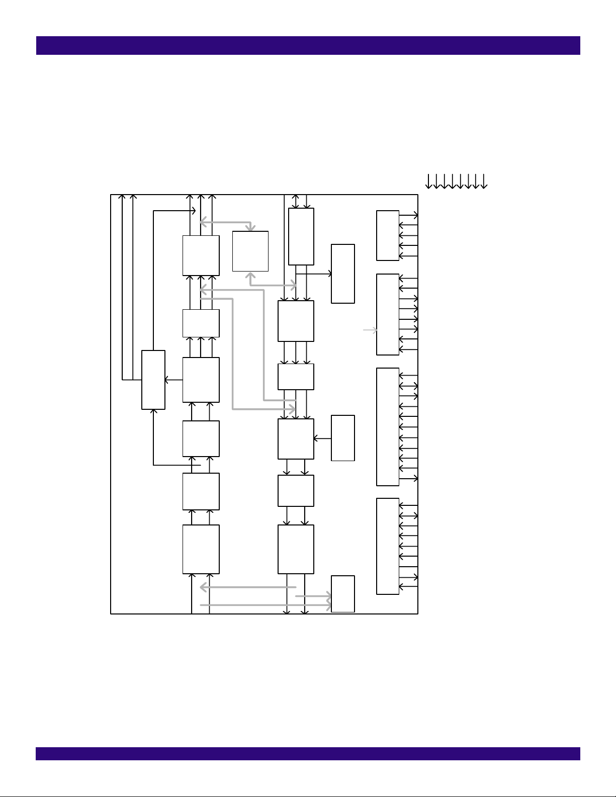
BLOCK DIAGRAM
VDDIO
VDDA
TCLK[28:0]/T DN[28:0]
TDN[28:0]/TMF[28:0]
LLOS
LLOS0
RCLK[28:0]/RMF[28:0]
RDN[28:0]/RMF[28:0]
RJA Decoder
RD[28:0]/RDP[28:0]
Pattern
Detec tor
Generator/
Digital Loopback
TD[28:0]/T DP[28:0]
TDO
TDI
Tx Clock
Recovery
Detec tor
Defect/Alarm
EncoderTJA
RCLK[28:0]
JTAG
Clock Generator
TCK
TMS
TRST
CLKB
CLKA
REF B
REF A
CLKE1
CLKT 1
MCKSEL[3:0]
MCLK
GNDA
VDDD
GNDD
GNDT
VDDT
VDDR
A[10:0]
D[7:0]
SDO/ACK/READY
SDI/R/ W/ WR
SCLK/ DS/RD
ALE/AS
IM
INT/ MOT
P/S
CS
INT
RST
GPIO[1:0]
TEHW
TEHWE
OE
RIM
REF
VCOM[1:0]
VCOMEN
Detec tor
Defect/Alarm
Rx Cl oc k &
Rx
RTIP[28:0]
Data
Equali zer Slicer
Recovery
Terminator
RRING[28:0]
Remote Loopback
Shaper
Waveform
Line
Driv er
Tx
Terminator
Analog
Loopback
TT IP[28:0]
TRING[28:0]
Alarm
G.772
Generator
Monitor
MCU InterfaceCommon Control
Figure-1 Functional Block Diagram
Block Diagram 12 January 11, 2007
IDT82P2828 28(+1) CHANNEL HIGH-DENSITY T1/E1/J1 LINE INTERFACE UNIT
1 PIN ASSIGNMENT
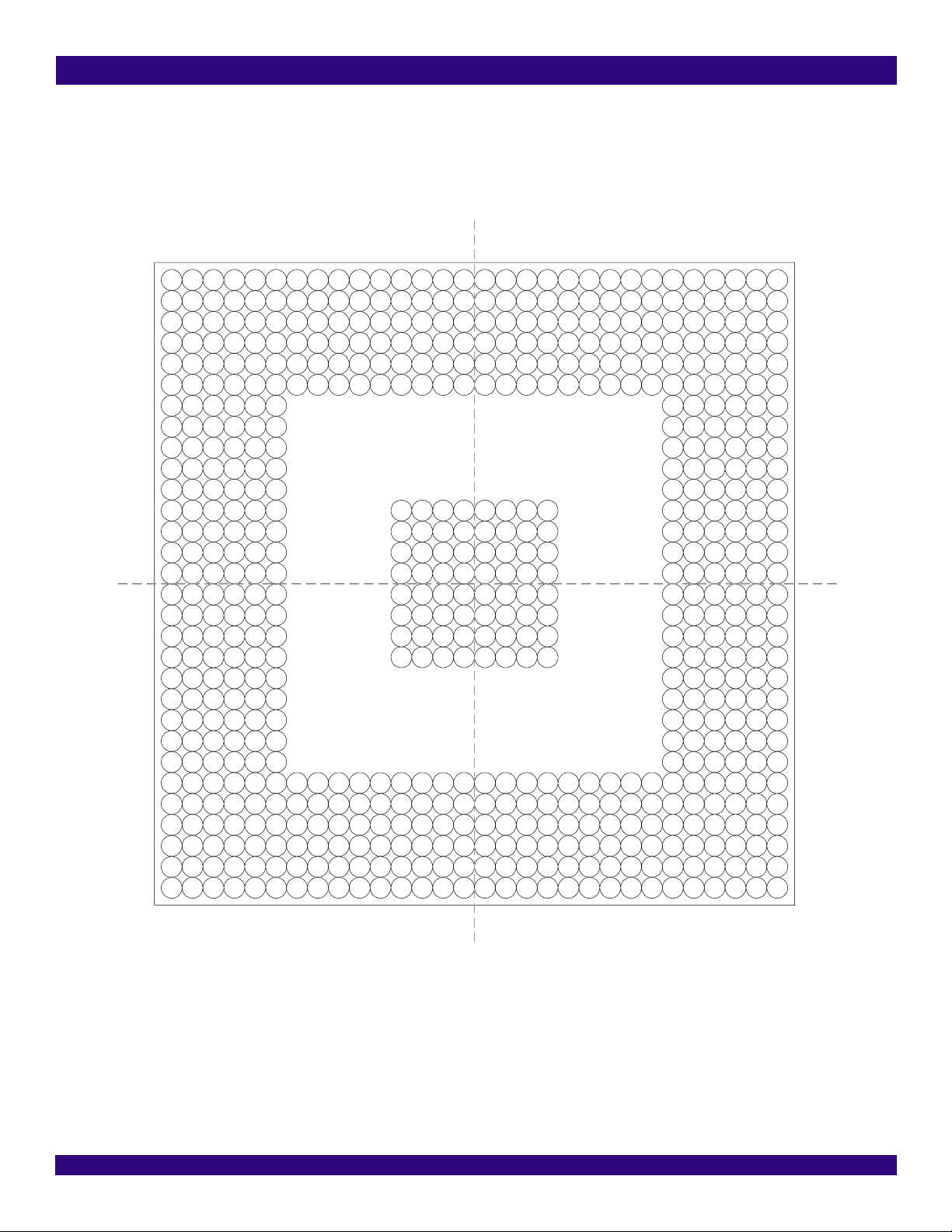
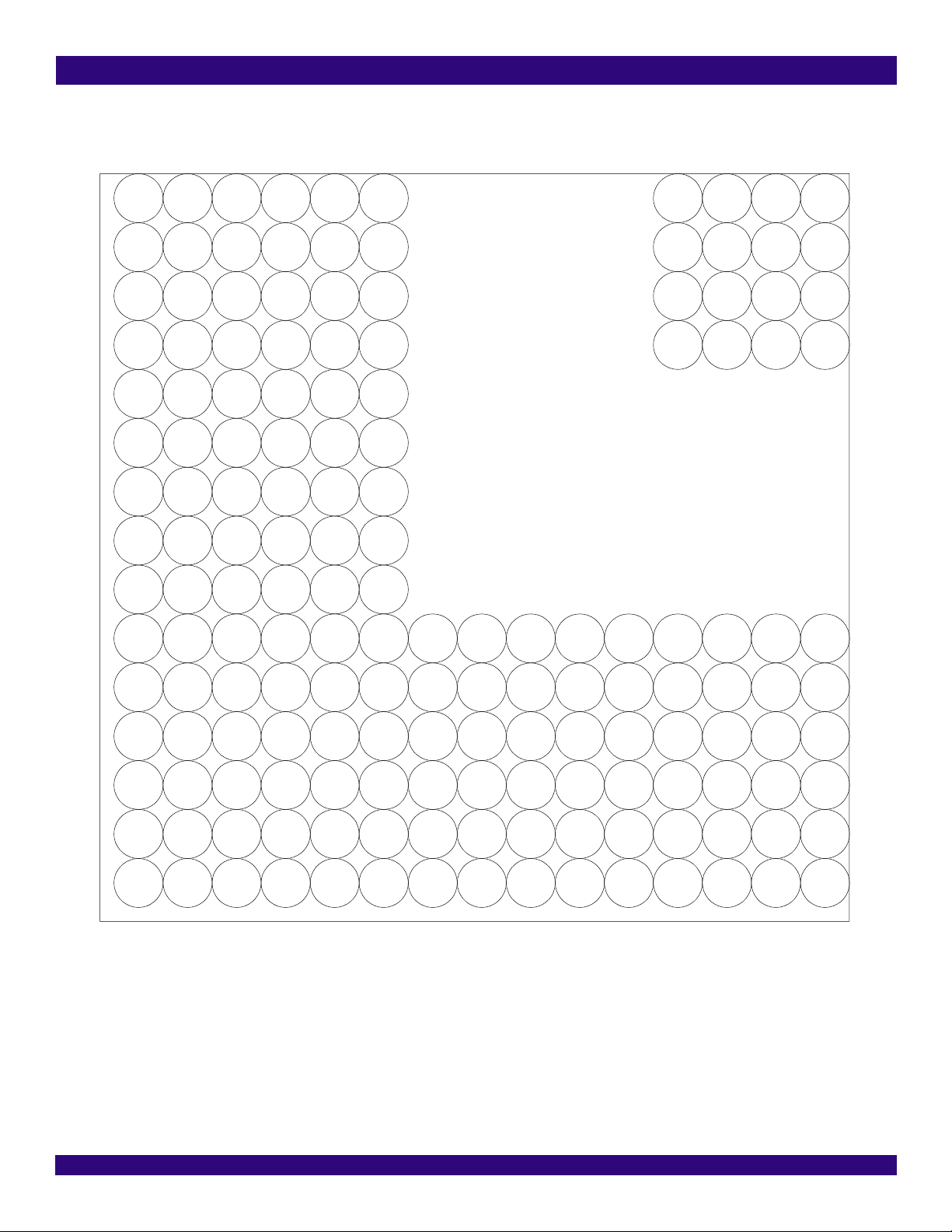
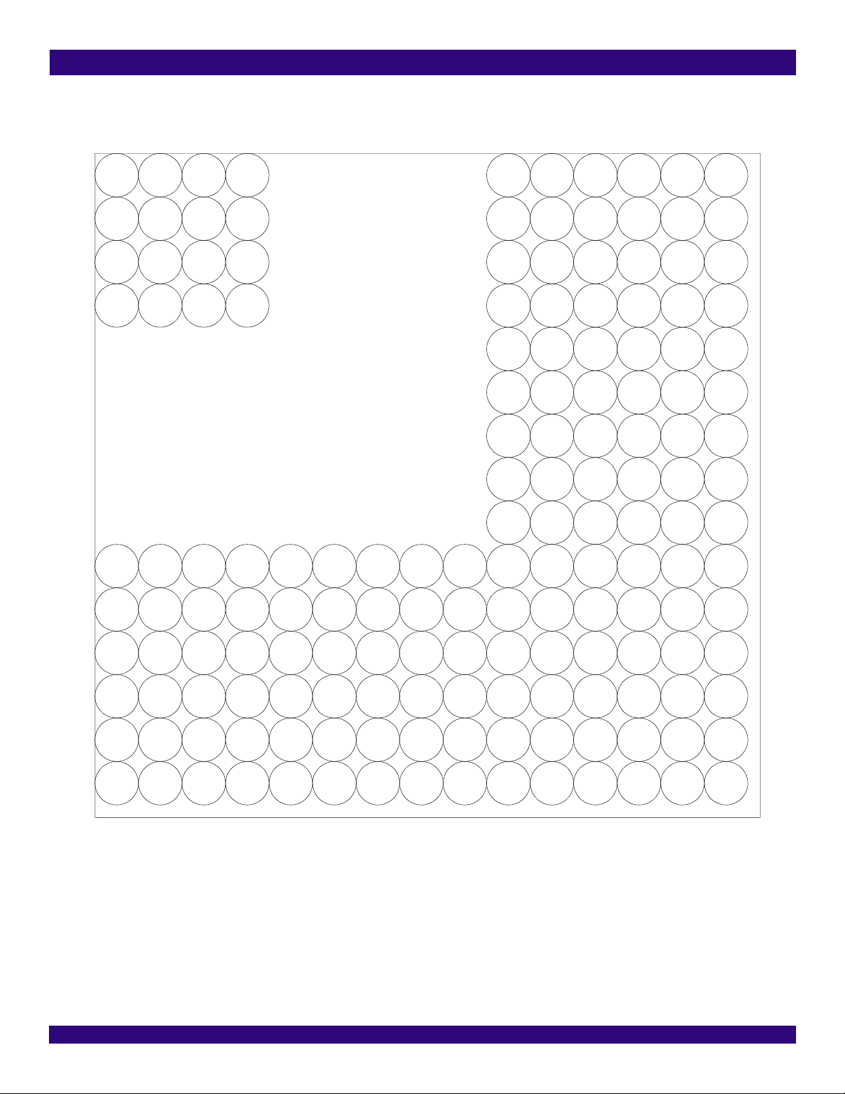
Figure-2 shows the outline of the pin assignment. For a clearer
description, four segments are divided in this figure and the details of
each are shown from Figure-3 to Figure-6.
1109876543212 262524232221201918171615141311 292827 30
A
B
C
D
E
F
G
H
J
K
L
M
N
P
R
T
U
V
W
Y
AA
AB
AC
AD
AE
AF
AG
AH
AJ
AK
Top
Left
Bottom
Left
Top
Right
Bottom
Right
A
B
C
D
E
F
G
H
J
K
L
M
N
P
R
T
U
V
W
Y
AA
AB
AC
AD
AE
AF
AG
AH
AJ
AK
1109876543212 262524232221201918171615141311 292827 30
Figure-2 640-Pin PBGA (Top View) - Outline
Pin Assignment 13 January 11, 2007
IDT82P2828 28(+1) CHANNEL HIGH-DENSITY T1/E1/J1 LINE INTERFACE UNIT
1111098765432 141312 15
TRING
A
B
C
D
E
F
G
H
J
K
GNDA TTIP23 TTIP22
GNDA
TTIP25
TRING
25
TRING
26
TTIP26
TRING
27
TTIP27
TTIP28
TRING0
TRING
TTIP24VDDA
24
24
24
24
26
28
TRING
VDDT
RTIP23
VDDR23VDDR
RRING25VDDR
RTIP25
VDDR
RRING
RTIP27 GNDTVDDT0
GNDT
23
GNDT
23
RRING
23
22
25
RRING
26
RTIP26
27
GNDTGNDT
27
TRING
VDDA GNDT
VDDT
GNDT
VDDT
VDDT
VDDT
VDDT
25
RTIP24GNDT RTIP22
RRING
VDDR
26
VDDR
27
VDDR
28
28
GNDT
22
VDDT
22
RRING
22
GNDA
GNDA
GNDA
GNDA
GNDA
TCLK28/
TDN28
TDN28/
TMF28
TD28/
TDP28
NC
RCLK28/
RDN28/
RDN27/
TD27/
TDP27
RMF28
TCLK27/
RMF28
RD28/
RDP28
VDDIO VDDIO VDDIO VDDIO
TCLK26/
RMF27
RD27/
RDP27
TDN27
TDN27/
TMF27
TDN26
TDN26/
TMF26
TD26/
TDP26
RCLK27/
RMF27
NCVDDIO VDDD VDDDNC
NC GNDDGNDAGNDA GNDD GNDD GNDDGNDDGNDD
TD25/
TDP25
RCLK26/
RMF26
RDN26/
RMF26
RD26/
RDP26
RDN25/
RMF25
RD25/
RDP25
TCLK25/
TDN25
TDN25/
TMF25
TCLK24/
TDN24
TDN24/
TMF24
TD24/
TDP24
RCLK25/
RMF25
TD23/
TDP23
RCLK24/
RMF24
RDN24/
RMF24
RD24/
RDP24
RDN23/
RMF23
RD23/
RDP23
TCLK23/
TDN23
TDN23/
TMF23
A
B
C
D
E
F
G
H
J
K
L
M
N
P
R
TTIP0
TTIP1
TRING2
TTIP2
TTIP3
VDDT1
GNDT
GNDT
VDDR0 VDDR1RRING0VDDT2
VDDR2 RRING1RTIP0VDDT3
VCOM0 RTIP1VDDT4TRING3
VDDA
VDDA RTIP28TRING1
RRING
28
GNDA
GNDA
GNDA
GNDA
GNDA
L
GNDDGNDDGNDDGNDD
GNDDGNDDGNDDGNDD
GNDDGNDDGNDDGNDD
GNDDGNDDGNDDGNDD
M
N
P
R
1111098765432 141312 15
Figure-3 640-Pin PBGA (Top View) - Top Left
Pin Assignment 14 January 11, 2007
IDT82P2828 28(+1) CHANNEL HIGH-DENSITY T1/E1/J1 LINE INTERFACE UNIT
3020 21 22 23 24 25 26 27 28 2917 18 1916
A
B
C
D
E
F
G
H
K
J
TDN22/
TMF22
TD22/
TDP22
RCLK23/
RMF23
NC
RCLK22/
RMF22
RDN22/
RMF22
RD22/
RDP22
TCLK22/
TDN22
VDDD
GNDD
RD21/
RDP21
TCLK21/
TDN21
TDN21/
TMF21
TD21/
TDP21
VDDD
GNDD
TDN20/
TMF20
TD20/
TDP20
RCLK21/
RMF21
RDN21/
RMF21
VDDD
GNDD
RCLK20/
RMF20
RDN20/
RMF20
RD20/
RDP20
TCLK20/
TDN20
RD19/
RDP19
TCLK19/
TDN19
TDN19/
TMF19
TD19/
TDP19
VDDIONCVDDD
GNDDGNDDGNDD
TDN18/
TMF18
TD18/
TDP18
RCLK19/
RMF19
RDN19/
RMF19
VDDIO
GNDD
RCLK18/
RMF18
RDN18/
RMF18
RD18/
RDP18
TCLK18/
TDN18
VDDIO
GNDD
RD17/
RDP17
TCLK17/
TDN17
TDN17/
TMF17
TD17/
TDP17
VDDIO
GNDD
TDN16/
TMF16
TD16/
TDP16
RCLK17/
RMF17
RDN17/
RMF17
GNDA
GNDA
GNDA
GNDA
RCLK16/
RMF16
RDN16/
TCLK16/
TCLK15/
RMF16
RD16/
RDP16
TDN16
VDDR21VDDR20
RRING
VDDR19
20
VDDR18RTIP20 VDDT19
NC GNDT GNDT
RRING
18
RCLK15/
RD15/
TD15/
19
VDDA
RMF15
RDN15/
RMF15
NC NC
GNDT REF
RRING
21
RTIP21 VDDT20GNDA
RRING
17
RDP15
TDN15
TDN15/
TMF15
TDP15
RRING
RTIP19VDDA GNDT VDDT18
GNDA
VDDT21VDDIO
TRING
19
VDDT17
GNDA
GNDAGNDA
TRING
21
TTIP21
TRING
20
TTIP20
TTIP19
TRING
18
TTIP18
TRING
17
A
B
C
D
E
F
G
H
J
K
VDDARTIP18 VDDT16
L
M
N
P
R
GNDDGNDDGNDDGNDD
GNDDGNDDGNDDGNDD
GNDDGNDDGNDDGNDD
GNDDGNDDGNDDGNDD
GNDA
GNDA
GNDA
GNDA
GNDA
VDDA
RRING
15
RRING
RTIP16VDDR17 GNDT GNDT
VDDR16
VDDR15RTIP15
RTIP17
16
VCOM1 VDDT15
RRING
GNDT
14
TRING
VDDT14
TTIP17
TTIP16
16
TRING
15
TTIP15
TRING
14
L
M
N
P
R
3020 21 22 23 24 25 26 27 28 2917 18 1916
Figure-4 640-Pin PBGA (Top View) - Top Right
Pin Assignment 15 January 11, 2007
IDT82P2828 28(+1) CHANNEL HIGH-DENSITY T1/E1/J1 LINE INTERFACE UNIT
1111098765432 141312 15
T
U
V
W
Y
AA
AB
AC
AD
AE
TRING4
TTIP4
TTIP5
TRING6
TTIP6
TTIP7
GNDA
TD1/
TDP1
RDN1/
RMF1
TCLK2/
TDN2
TDN1/
TMF1
RCLK1/
RMF1
RD2/
RDP2
RRING5
RTIP5
GNDT
TCLK1/
TDN1
TD2/
TDP2
RDN2/
RMF2
VDDA VDDR3RRING2GNDT
RRING3 VDDR4RTIP2GNDT
RTIP3 RRING4VDDT5TRING5
VDDA RTIP4VDDT6
RRING6 VDDAVDDT7
RTIP6 RRING7TRING7
VDDR6 RTIP7VDDR5GNDT
RD1/
RDP1
TDN2/
TMF2
RCLK2/
RMF2
GNDA GNDDGNDDGNDDGNDD
GNDA
GNDA
GNDA
GNDA
GNDA
GNDA
VDDR7
VDDA
GNDA
GNDA
TMS GNDA
VDDIO VDDIOGNDDGNDD VDDD VDDD VDDIOGNDDGNDD
T
GNDDGNDDGNDDGNDD
GNDDGNDDGNDDGNDD
GNDDGNDDGNDDGNDD
U
V
W
Y
AA
AB
AC
AD
AE
AF
AG
AH
AJ
AK
TD3/
TDP3
RD3/
RDP3
RDN3/
RMF3
GNDA
GNDA
TDN3/
RCLK3/
VDDA
VDDA D7 A6 A2A10D3
TMF3
TD4/
TDP4
RMF3
TCLK3/
TDN3
RDN4/
RMF4
RD4/
RDP4
TCLK4/
TDN4
TDN4/
TMF4
TRST TDI
TCLK5/
TDN5
TDN5/
TMF5
TD5/
TDP5
RCLK4/
RMF4
TDP6
RCLK5/
RMF5
RDN5/
RMF5
RDP5
TD6/
RD5/
TCK
RDN6/
RMF6
RD6/
RDP6
TCLK6/
TDN6
TDN6/
TMF6
TCLK7/
TDN7
TDN7/
TMF7
TD7/
TDP7
RCLK6/
RMF6
TD0/
TDP0
RCLK7/
RMF7
RDN7/
RMF7
RD7/
RDP7
GPIO0 GPIO1NCTDO TEHWE INT/MOT IMICTEHW
RDN0/
RMF0
RD0/
RDP0
TCLK0/
TDN0
TDN0/
TMF0
RST D4 A3 ALE/ASA7D0
RIM
OE
RCLK0/
RMF0
D5 A4 A0A8D1
D6 A5 A1A9D2
1111098765432 141312 15
Figure-5 640-Pin PBGA (Top View) - Bottom Left
AF
AG
AH
AJ
AK
Pin Assignment 16 January 11, 2007
IDT82P2828 28(+1) CHANNEL HIGH-DENSITY T1/E1/J1 LINE INTERFACE UNIT
3020 21 22 23 24 25 26 27 28 2917 18 1916
U
V
W
Y
AA
AB
AC
AD
AE
T
GNDDGNDDGNDDGNDD
GNDDGNDDGNDDGNDD
GNDDGNDDGNDDGNDD
VDDIOVDDD VDDIO VDDIOVDDDVDDIOVDDIO VDDIO VDDD
GNDAGNDDGNDDGNDDGNDD
GNDA
GNDA
GNDA
GNDA
GNDA
GNDA
GNDA
GNDA
VDDR14VDDR13 RTIP14 VDDT13
RRING
VDDR12
13
GNDA GNDT
RRING
GNDA GNDT
RRING
VDDA
11
VDDARTIP11 VDDT11
RRING
RTIP10GNDA VDDT10 VDDT9
VDDR11RRING9 RRING8 GNDT
VDDR10RTIP9 RTIP8 GNDTGNDA
GNDT
NCRTIP13 GNDT GNDT
RTIP12
12
VDDA
VDDA
10
TRING
VDDT12
TRING
TTIP14
TTIP13
13
TRING
12
TTIP12
TRING
11
TTIP11
TTIP10
10
TRING9
TTIP9
TRING8
T
U
V
W
Y
AA
AB
AC
AD
AE
AF
AG
AH
AJ
AK
LLOSNC LLOS0
CLKBP/S CLKE1
SDI/R/W/
SDO/
ACK/
RDY
CLKA
CS
CLKT1
REFB
WR
SCLK/
INT REFA MCLK
DS/RD
MCKSEL
0
TCLK8/
TDN8
TDN8/
TMF8
TD8/
TDP8
MCKSEL
1
TD9/
TDP9
RCLK8/
RMF8
RDN8/
RMF8
RD8/
RDP8
MCKSEL
2
RDN9/
RMF9
RD9/
RDP9
TCLK9/
TDN9
TDN9/
TMF9
MCKSEL
3
TCLK10/
TDN10
TDN10/
TMF10
TD10/
TDP10
RCLK9/
RMF9
GNDD GNDD
RDN11/
TD11/
TDP11
RCLK10/
RMF10
RDN10/
RMF10
RD10/
RDP10
RMF11
RD11/
RDP11
TCLK11/
TDN11
TDN11/
TMF11
TCLK12/
TDN12
TDN12/
TMF12
TD12/
TDP12
RCLK11/
RMF11
Figure-6 640-Pin PBGA (Top View) - Bottom Right
VCOME
N
TD13/
TDP13
RCLK12/
RMF12
RDN12/
RMF12
RD12/
RDP12
VDDR9
RDN13/
RMF13
RD13/
RDP13
TCLK13/
TDN13
TDN13/
TMF13
VDDR8 VDDT8NC
TCLK14/
TDN14
TDN14/
TMF14
TD14/
TDP14
RCLK13/
RMF13
RCLK14/
RMF14
RD14/
RDP14
GNDA
GNDA
TTIP8
NC
RDN14/
RMF14
GNDA
GNDA
3020 21 22 23 24 25 26 27 28 2917 18 1916
AF
AG
AH
AJ
AK
Pin Assignment 17 January 11, 2007

IDT82P2828 28(+1) CHANNEL HIGH-DENSITY T1/E1/J1 LINE INTERFACE UNIT
2 PIN DESCRIPTION
Name I / O
RTIPn
RRINGn
(n=0~28)
TTIPn
Output L1, M1, P1, R1, U1, V1, Y1, AA1,
TRINGn
(n=0~28)
1
Pin No.
Input P3, R5, U3, V4, W5, Y3, AA4, AB5,
AE28, AE26, AC27, AA26, W28,
V26, T28, R26, N27, L28, L26, J27,
G26, F28, D6, D4, D3, G4, H5, K4,
M5
N3, P5, T3, U4, V5, W3, Y4, AA5,
AD28, AD26, AB27, Y26, W27,
U26, R28, P26, M27, K28, K26,
H27, F26, E28, E6, D5, E3, F4, G5,
J4, L5
AF30, AD30, AB30, AA30, W30,
U30, T30, P30, M30, L30, J30, G30,
F30, D30, A5, A4, A3, C1, F1, H1,
J1
K1, M2, N1, R2, T1, V2, W1, AA2,
AE30, AC30, AB29, Y30, V30, U29,
R30, N30, M29, K30, H30, G29,
E30, C30, A6, B4, B3, D1, E1, G1,
J2
Description
Line Interface
RTIPn / RRINGn: Receive Bipolar Tip/Ring for Channel 0 ~ 28
The receive line interface supports both Receive Differential mode and Receive Single Ended
mode.
In Receive Differential mode, the received signal is coupled into RTIPn and RRINGn via a 1:1
transformer or without a transformer (transformer-less).
In Receive Single Ended mode, RRINGn should be left open. The received signal is input on
RTIPn via a 2:1 (step down) transformer or without a transformer (transformer-less).
These pins will become High-Z globally or channel specific in the following conditions:
• Global High-Z:
- Connecting the RIM pin to low;
- Loss of MCLK
- During and after power-on reset, hardware reset or global software reset;
• Per-channel High-Z
- Receiver power down by writing ‘1’ to the R_OFF bit (b5, RCF0,...)
TTIPn / TRINGn: Transmit Bipolar Tip /Ring for Channel 0 ~ 28
The transmit line interface supports both Transmit Differential mode and Transmit Single
Ended mode.
In Transmit Differential mode, TTIPn outputs a positive differential pulse while TRINGn outputs a negative differential pulse. The pulses are coupled to the line side via a 1:2 (step up)
transformer or without a transformer (transformer-less).
In Transmit Single Ended mode, TRINGn should be left open (it is shorted to ground internally). The signal presented at TTIPn is output to the line side via a 1:2 (step up) transformer.
These pins will become High-Z globally or channel specific in the following conditions:
• Global High-Z:
- Connecting the OE pin to low;
- Loss of MCLK;
- During and after power-on reset, hardware reset or global software reset;
• Per-channel High-Z
2
- Writing ‘0’ to the OE bit (b6, TCF0,...)
;
- Loss of TCLKn in Transmit Single Rail NRZ Format mode or Transmit Dual Rail NRZ
Format mode, except that the channel is in Remote Loopback or transmit internal pat-
3
tern with XCLK
;
- Transmitter power down by writing ‘1’ to the T_OFF bit (b5, TCF0,...);
- Per-channel software reset;
- The THZ_OC bit (b4, TCF0,...) is set to ‘1’ and the transmit driver over-current is
detected.
Refer to Section 3.3.8 Output High-Z on TTIP and TRING for details.
Note:
1. The pin number of the pins with the footnote ‘n’ is listed in order of channel (CH0 ~ CH28).
2. The content in the brackets indicates the position and the register name of the preceding bit. After the register name, if the punctuation ‘,...’ is followed, this bit is in a per-channel register.
If there is no punctuation following the address, this bit is in a global register or in a channel 0 only register. The addresses and details are included in Chapter 5 Programming Information.
3. XCLK is derived from MCLK. It is 1.544 MHz in T1/J1 mode or 2.048 MHz in E1 mode.
Pin Description 18 January 11, 2007

IDT82P2828 28(+1) CHANNEL HIGH-DENSITY T1/E1/J1 LINE INTERFACE UNIT
Name I / O Pin No. Description
System Interface
RDn / RDPn
(n=0~28)
RDNn / RMFn
(n=0~28)
Output AH9, AC4, AE2, AG1, AH3, AK5,
AH6, AK8, AK20, AH21, AK23,
AH24, AK26, AH27, AH29, A27,
C26, A24, C23, A21, C20, A18,
C17, B15, D14, B12, D11, B9, D8
Output AG9, AD1, AE3, AH1, AG3, AJ5,
AG6, AJ8, AJ20, AG21, AJ23,
AG24, AJ26, AG27, AH30, B28,
B26, D25, B23, D22, B20, D19,
B17, A15, C14, A12, C11, A9, C8
RDn: Receive Data for Channel 0 ~ 28
When the receive system interface is configured to Single Rail NRZ Format mode, this multiplex pin is used as RDn.
The decoded NRZ data is updated on the active edge of RCLKn. The active level on RDn is
selected by the RD_INV bit (b3, RCF1,...).
When the receiver is powered down, RDn will be in High-Z state or low, as selected by the
RHZ bit (b6, RCF0,...).
RDPn: Positive Receive Data for Channel 0 ~ 28
When the receive system interface is configured to Dual Rail NRZ Format mode, Dual Rail RZ
Format mode or Dual Rail Sliced mode, this multiplex pin is used as RDPn.
In Receive Dual Rail NRZ Format mode, the un-decoded NRZ data is output on RDPn and
RDNn and updated on the active edge of RCLKn.
In Receive Dual Rail RZ Format mode, the un-decoded RZ data is output on RDPn and RDNn
and updated on the active edge of RCLKn.
In Receive Dual Rail Sliced mode, the raw RZ sliced data is output on RDPn and RDNn.
For Receive Differential line interface, an active level on RDPn indicates the receipt of a positive pulse on RTIPn and a negative pulse on RRINGn; while an active level on RDNn indicates the receipt of a negative pulse on RTIPn and a positive pulse on RRINGn.
For Receive Single Ended line interface, an active level on RDPn indicates the receipt of a
positive pulse on RTIPn; while an active level on RDNn indicates the receipt of a negative
pulse on RTIPn.
The active level on RDPn and RDNn is selected by the RD_INV bit (b3, RCF1,...).
When the receiver is powered down, RDPn and RDNn will be in High-Z state or low, as
selected by the RHZ bit (b6, RCF0,...).
RDNn: Negative Receive Data for Channel 0 ~ 28
When the receive system interface is configured to Dual Rail NRZ Format mode, Dual Rail RZ
Format mode or Dual Rail Sliced mode, this multiplex pin is used as RDNn.
(Refer to the description of RDPn for details).
RMFn: Receive Multiplex Function for Channel 0 ~ 28
When the receive system interface is configured to Single Rail NRZ Format mode, this multiplex pin is used as RMFn.
RMFn is configured by the RMF_DEF[2:0] bits (b7~5, RCF1,...) and can indicate PRBS/ARB,
LAIS, LEXZ, LBPV, LEXZ+LBPV, LLOS, output recovered clock (RCLK) or XOR output of
positive and negative sliced data. Refer to Section 3.5.7.1 RMFn Indication for details.
The output on RMFn is updated on the active edge of RCLKn. The active level of RMFn is
always high.
When the receiver is powered down, RMFn will be in High-Z state or low, as selected by the
RHZ bit (b6, RCF0,...).
Pin Description 19 January 11, 2007

IDT82P2828 28(+1) CHANNEL HIGH-DENSITY T1/E1/J1 LINE INTERFACE UNIT
Name I / O Pin No. Description
RCLKn / RMFn
(n=0~28)
LLOS Output AF17 LLOS: Receive Line Loss Of Signal
LLOS0 Output AF18 LLOS0: Receive Line Loss Of Signal for Channel 0
Output AK10, AD2, AE4, AH2, AK4, AH5,
AK7, AH8, AH20, AK22, AH23,
AK25, AH26, AK28, AG29, A28,
A26, C25, A23, C22, A20, C19,
A17, C16, B14, D13, B11, D10, B8
RCLKn: Receive Clock for Channel 0 ~ 28
When the receive system interface is configured to Single Rail NRZ Format mode, Dual Rail
NRZ Format mode or Dual Rail RZ Format mode, this multiplex pin is used as RCLKn.
RCLKn outputs a 1.544 MHz (in T1/J1 mode) or 2.048 MHz (in E1 mode) clock which is
recovered from the received signal.
The data output on RDn and RMFn (in Receive Single Rail NRZ Format mode) or RDPn/
RDNn (in Receive Dual Rail NRZ Format mode, Receive Dual Rail RZ Format mode and
Receive Dual Rail Sliced) is updated on the active edge of RCLKn. The active edge is
selected by the RCK_ES bit (b4, RCF1,...).
In LLOS condition, RCLKn output high or XCLK,
RCF0,...) (refer to Section 3.5.3.1 Line LOS (LLOS) for details).
When the receiver is powered down, RCLKn will be in High-Z state or low, as selected by the
RHZ bit (b6, RCF0,...).
RMFn: Receive Multiplex Function for Channel 0 ~ 28
When the receive system interface is configured to Dual Rail Sliced mode, this multiplex pin is
used as RMFn.
(Refer to the description of RMFn of the RDNn/RMFn multiplex pin for details).
LLOS synchronizes with the output of CLKE1 and can indicate the LLOS (Line LOS) status of
all 29 channels in a serial format.
When the clock output on CLKE1 is enabled, LLOS indicates the LLOS status of the 29 channels in a serial format and repeats every twenty-nine cycles. Channel 0 is positioned by
LLOS0. Refer to the description of LLOS0 below for details.
LLOS is updated on the rising edge of CLKE1 and is always active high.
When the clock output of CLKE1 is disabled, LLOS will be held in High-Z state.
(Refer to Section 3.5.3.1 Line LOS (LLOS) for details.)
LLOS0 can indicate the position of channel 0 on the LLOS pin.
When the clock output on CLKE1 is enabled, LLOS0 pulses high for one CLKE1 clock cycle to
indicate the position of channel 0 on the LLOS pin. When CLKE1 outputs 8 KHz clock, LLOS0
pulses high for one 8 KHz clock cycle (125 µs) every twenty-nine 8 KHz clock cycles; when
CLKE1 outputs 2.048 MHz clock, LLOS0 pulses high for one 2.048 MHz clock cycle (488 ns)
every twenty-nine 2.048 MHz clock cycles. LLOS0 is updated on the rising edge of CLKE1.
When the clock output on CLKE1 is disabled, LLOS0 will be held in High-Z state.
(Refer to Section 3.5.3.1 Line LOS (LLOS) for details.)
as selected by the RCKH bit (b7,
Pin Description 20 January 11, 2007

IDT82P2828 28(+1) CHANNEL HIGH-DENSITY T1/E1/J1 LINE INTERFACE UNIT
Name I / O Pin No. Description
TDn / TDPn
(n=0~28)
TDNn / TMFn
(n=0~28)
TCLKn / TDNn
(n=0~28)
Input AG8, AC1, AD3, AF1, AG2, AJ4,
AG5, AJ7, AJ19, AG20, AJ22,
AG23, AJ25, AG26, AJ28, D27,
B25, D24, B22, D21, B19, D18,
B16, A14, C13, A11, C10, A8, C7
Input / Output AK9, AC2, AD4, AF2, AK3, AH4,
AK6, AH7, AH19, AK21, AH22,
AK24, AH25, AK27, AH28, C27,
A25, C24, A22, C21, A19, C18,
A16, D15, B13, D12, B10, D9, B7
Input AJ9, AC3, AE1, AF3, AJ3, AG4,
AJ6, AG7, AG19, AJ21, AG22,
AJ24, AG25, AJ27, AG28, B27,
D26, B24, D23, B21, D20, B18,
D17, C15, A13, C12, A10, C9, A7
TDn: Transmit Data for Channel 0 ~ 28
When the transmit system interface is configured to Single Rail NRZ Format mode, this multiplex pin is used as TDn.
TDn accepts Single Rail NRZ data. The data is sampled into the device on the active edge of
TCLKn.
The active level on TDn is selected by the TD_INV bit (b3, TCF1,...).
TDPn: Positive Transmit Data for Channel 0 ~ 28
When the transmit system interface is configured to Dual Rail NRZ Format mode or Dual Rail
RZ Format mode, this multiplex pin is used as TDPn.
In Transmit Dual Rail NRZ Format mode, the pre-encoded NRZ data is input on TDPn and
TDNn and sampled on the active edge of TCLKn.
In Transmit Dual Rail RZ Format mode, the pre-encoded RZ data is input on TDPn and TDNn.
The line code is as follows (when the TD_INV bit (b3, TCF1,...) is ‘0’):
TDPn TDNn Output Pulse on TTIPn Output Pulse on TRINGn *
0 0 Space Space
0 1 Negative Pulse Positive Pulse
1 0 Positive Pulse Negative Pulse
1 1 Space Space
Note:
* For Transmit Single Ended line interface, TRINGn should be open.
The active level on TDPn and TDNn is selected by the TD_INV bit (b3, TCF1,...).
TDNn: Negative Transmit Data for Channel 0 ~ 28
When the transmit system interface is configured to Dual Rail NRZ Format mode, this multiplex pin is used as TDNn.
(Refer to the description of TDPn for details).
TMFn: Transmit Multiplex Function for Channel 0 ~ 28
When the transmit system interface is configured to Single Rail NRZ Format mode or Dual
Rail RZ Format mode, this multiplex pin is used as TMFn.
TMFn is configured by the TMF_DEF[2:0] bits (b7~5, TCF1,...) and can indicate PRBS/ARB,
SAIS, TOC, TLOS, SEXZ, SBPV, SEXZ+SBPV, SLOS. Refer to Section 3.5.7.2 TMFn Indication for details.
The output on TMFn is updated on the active edge of TCLKn (if available). The active level of
TMFn is always high.
TCLKn: Transmit Clock for Channel 0 ~ 28
When the transmit system interface is configured to Single Rail NRZ Format mode or Dual
Rail NRZ Format mode, this multiplex pin is used as TCLKn.
TCLKn inputs a 1.544 MHz (in T1/J1 mode) or 2.048 MHz (in E1 mode) clock.
The data input on TDn (in Transmit Single Rail NRZ Format mode) or TDPn/TDNn (in Transmit Dual Rail NRZ Format mode) is sampled on the active edge of TCLKn. The data output on
TMFn (in Transmit Single Rail NRZ Format mode) is updated on the active edge of TCLKn.
The active edge is selected by the TCK_ES bit (b4, TCF1,...).
TDNn: Negative Transmit Data for Channel 0 ~ 28
When the transmit system interface is configured to Dual Rail RZ Format mode, this multiplex
pin is used as TDNn.
(Refer to the description of TDPn for details).
Pin Description 21 January 11, 2007
IDT82P2828 28(+1) CHANNEL HIGH-DENSITY T1/E1/J1 LINE INTERFACE UNIT
Name I / O Pin No. Description
Clock
MCLK Input AK19 MCLK: Master Clock Input
MCLK provides a stable reference timing for the IDT82P2828. MCLK should be a jitter-free
clock with ±32 ppm (in T1/J1 mode) or ±50 ppm (in E1 mode) accuracy. The clock frequency
of MCLK is informed to the device by MCKSEL[3:0].
If MCLK misses (duty cycle is less than 30% for 10 µs) and then recovers, the device will be
reset automatically.
MCKSEL[0]
Input AF19
MCKSEL[3:0]: Master Clock Selection
These four pins inform the device of the clock frequency input on MCLK:
MCKSEL[1]
AF20
MCKSEL[3:0]
MCKSEL[2]
MCKSEL[3]
AF21
AF22
*
Frequency (MHz)
0000 1.544
0001 1.544 X 2
0010 1.544 X 3
0011 1.544 X 4
0100 1.544 X 5
0101 1.544 X 6
0110 1.544 X 7
0111 1.544 X 8
1000 2.048
1001 2.048 X 2
1010 2.048 X 3
1011 2.048 X 4
1
Note:
0: GNDD
1: VDDIO
CLKT1 Output AH18 CLKT1: 8 KHz / T1 Clock Output
The output on CLKT1 can be enabled or disabled, as determined by the CLKT1_EN bit (b1,
CLKG).
When the output is enabled, CLKT1 outputs an 8 KHz or 1.544 MHz clock, as selected by the
CLKT1 bit (b0, CLKG). The output is locked to MCLK.
When the output is disabled, CLKT1 is in High-Z state.
CLKE1 Output AG18 CLKE1: 8 KHz / E1 Clock Output
The output on CLKE1 can be enabled or disabled, as determined by the CLKE1_EN bit (b3,
CLKG).
When the output is enabled, CLKE1 outputs an 8 KHz or 2.048 MHz clock, as selected by the
CLKE1 bit (b2, CLKG). The output is locked to MCLK.
When the output is disabled, CLKE1 is in High-Z state.
Note:
1. jitter is no more than 0.001 UI.
1100 2.048 X 5
1101 2.048 X 6
1110 2.048 X 7
1111 2.048 X 8
Pin Description 22 January 11, 2007

IDT82P2828 28(+1) CHANNEL HIGH-DENSITY T1/E1/J1 LINE INTERFACE UNIT
Name I / O Pin No. Description
REFA Output AK18 REFA: Reference Clock Output A
REFA can output three kinds of clocks: a recovered clock of one of the 29 channels, an external clock input on CLKA or a free running clock. The clock frequency is programmable. Refer
to Section 3.6.2 Clock Outputs on REFA/REFB for details.
The output on REFA can also be disabled, as determined by the REFA_EN bit (b6, REFA).
When the output is disabled, REFA is in High-Z state.
REFB Output AJ18 REFB: Reference Clock Output B
REFB can output a recovered clock of one of the 29 channels, an external clock input on
CLKB or a free running clock. Refer to Section 3.6.2 Clock Outputs on REFA/REFB for
details.
The output on REFB can also be disabled, as determined by the REFB_EN bit (b6, REFB).
When the output is disabled, REFB is in High-Z state.
CLKA Input AH17 CLKA: External T1/E1 Clock Input A
External T1/J1 (1.544 MHz) or E1 (2.048 MHz) clock is input on this pin. The CKA_T1E1 bit
(b5, REFA) should be set to match the clock frequency.
When not used, this pin should be connected to GNDD.
CLKB Input AG17 CLKB: External T1/E1 Clock Input B
External T1/J1 (1.544 MHz) or E1 (2.048 MHz) clock is input on this pin. The CKB_T1E1 bit
(b5, REFB) should be set to match the clock frequency.
When not used, this pin should be connected to GNDD.
Common Control
VCOM[0]
VCOM[1]
VCOMEN Input
REF - D29 REF: Reference Resistor
RIM Input
Output R4
(Pull-Down)
(Pull-Down)
VCOM: Voltage Common Mode [1:0]
These pins are used only when the receive line interface is in Receive Differential mode and
P28
AF26 VCOMEN: Voltage Common Mode Enable
AH10 RIM: Receive Impedance Matching
connected without a transformer (transformer-less).
To enable these pins, the VCOMEN pin must be connected high. Refer to Figure-10 for the
connection.
When these pins are not used, they should be left open.
This pin should be connected high only when the receive line interface is in Receive Differential mode and connected without a transformer (transformer-less).
When not used, this pin should be left open.
An external resistor (10 KΩ, ±1%) is used to connect this pin to ground to provide a standard
reference current for internal circuit. This resistor is required to ensure correct device operation.
In Receive Differential mode, when RIM is low, all 29 receivers become High-Z and only external impedance matching is supported. In this case, the per-channel impedance matching configuration bits - the R_TERM[2:0] bits (b2~0, RCF0,...) and the R120IN bit (b4, RCF0,...) - are
ignored.
In Receive Differential mode, when RIM is high, impedance matching is configured on a perchannel basis by the R_TERM[2:0] bits (b2~0, RCF0,...) and the R120IN bit (b4, RCF0,...).
This pin can be used to control the receive impedance state for Hitless Protection applications. Refer to Section 4.4 Hitless Protection Switching (HPS) Summary for details.
In Receive Single Ended mode, this pin should be left open.
Pin Description 23 January 11, 2007

IDT82P2828 28(+1) CHANNEL HIGH-DENSITY T1/E1/J1 LINE INTERFACE UNIT
Name I / O Pin No. Description
OE Input AJ10 OE: Output Enable
OE enables or disables all Line Drivers globally.
A high level on this pin enables all Line Drivers while a low level on this pin places all Line
Drivers in High-Z state and independent from related register settings.
Note that the functionality of the internal circuit is not affected by OE.
If this pin is not used, it should be tied to VDDIO.
This pin can be used to control the transmit impedance state for Hitless protection applications. Refer to Section 4.4 Hitless Protection Switching (HPS) Summary for details.
TEHWE Input
(Pull-Up)
TEHW Input
(Pull-Up)
GPIO[0]
GPIO[1]
RST Input AG10 RST: Reset (Active Low)
Output / Input AF9
AF11 TEHWE: Hardware T1/J1 or E1 Mode Selection Enable
When this pin is open, the T1/J1 or E1 operation mode is selected by TEHW globally.
When this pin is low, the T1/J1 or E1 operation mode is selected by the T1E1 bit (b0,
CHCF,...) on a per-channel basis.
AF12 TEHW: Hardware T1/J1 or E1 Mode Selection
When TEHWE is open, this pin selects the T1/J1 or E1 operation mode globally:
Low - E1 mode;
Open - T1/J1 mode.
When TEHWE is low, the input on this pin is ignored.
GPIO: General Purpose I/O [1:0]
These two pins can be defined as input pins or output pins by the DIR[1:0] bits (b1~0, GPIO)
AF10
respectively.
When the pins are input, their polarities are indicated by the LEVEL[1:0] bits (b3~2, GPIO)
respectively.
When the pins are output, their polarities are controlled by the LEVEL[1:0] bits (b3~2, GPIO)
respectively.
A low pulse on this pin resets the device. This hardware reset process completes in 2 µs maximum. Refer to Section 4.1 Reset for an overview on reset options.
MCU Interface
INT Output AK16 INT: Interrupt Request
This pin indicates interrupt requests for all unmasked interrupt sources.
The output characteristics (open drain or push-pull internally) and the active level are determined by the INT_PIN[1:0] bits (b3~2, GCF).
CS Input AJ17 CS: Chip Select (Active Low)
This pin must be asserted low to enable the microprocessor interface.
A transition from high to low must occur on this pin for each Read/Write operation and CS
should remain low until the operation is over.
P/S Input AG16 P/S: Parallel or Serial Microprocessor Interface Select
P/S selects Serial or Parallel microprocessor interface for the device:
GNDD - Serial microprocessor interface.
VDDIO - Parallel microprocessor interface.
Serial microprocessor interface consists of the CS, SCLK, SDI, SDO pins.
Parallel microprocessor interface consists of the CS, INT/MOT, IM, DS/RD, ALE/AS, R/W/WR,
ACK/RDY, D[7:0], A[10:0] pins.
INT/MOT Input
(Pull-Up)
AF14 INT/MOT: Intel or Motorola Microprocessor Interface Select
In Parallel microprocessor interface, INT/MOT selects Intel or Motorola microprocessor interface for the device:
GNDD - Parallel Motorola microprocessor interface.
Open - Parallel Intel microprocessor interface.
In Serial microprocessor interface, this pin should be left open.
Pin Description 24 January 11, 2007

IDT82P2828 28(+1) CHANNEL HIGH-DENSITY T1/E1/J1 LINE INTERFACE UNIT
Name I / O Pin No. Description
IM Input
(Pull-Up)
ALE / AS Input AG15 ALE: Address Latch Enable
SCLK / DS / RD Input AK17 SCLK: Shift Clock
AF15 IM: Interface Mode Selection
In Parallel Motorola or Intel microprocessor interface, IM selects multiplexed bus or non-multiplexed bus for the device:
GNDD - Parallel Motorola /Intel Non-Multiplexed microprocessor interface.
Open - Parallel Motorola /Intel Multiplexed microprocessor interface.
In Serial microprocessor interface, this pin should be connected to GNDD.
In Parallel Intel Multiplexed microprocessor interface, this multiplex pin is used as ALE.
The address on A[10:8] and D[7:0] (A[7:0] are ignored) is sampled into the device on the falling edges of ALE.
AS: Address Strobe
In Parallel Motorola Multiplexed microprocessor interface, this multiplex pin is used as AS.
The address on A[10:8] and D[7:0] (A[7:0] are ignored) is latched into the device on the falling
edges of AS.
In Parallel Motorola /Intel Non-Multiplexed microprocessor interface, this pin should be pulled
high.
In Serial microprocessor interface, this pin should be connected to GNDD.
In Serial microprocessor interface, this multiplex pin is used as SCLK.
SCLK inputs the shift clock for the Serial microprocessor interface. Data on SDI is sampled by
the device on the rising edge of SCLK. Data on SDO is updated on the falling edge of SCLK.
DS: Data Strobe (Active Low)
In Parallel Motorola microprocessor interface, this multiplex pin is used as DS.
During a write operation (R/W = 0), data on D[7:0] is sampled into the device. During a read
operation (R/W = 1), data is driven to D[7:0] by the device.
RD: Read Strobe (Active Low)
In Parallel Intel microprocessor interface, this multiplex pin is used as RD.
RD is asserted low by the microprocessor to initiate a read operation. Data is driven to D[7:0]
by the device during the read operation.
SDI / R/W / WR Input AH16 SDI: Serial Data Input
In Serial microprocessor interface, this multiplex pin is used as SDI.
Address and data on this pin are serially clocked into the device on the rising edge of SCLK.
R/W: Read / Write Select
In Parallel Motorola microprocessor interface, this multiplex pin is used as R/W.
R/W is asserted low for write operation or high for read operation.
WR: Write Strobe (Active Low)
In Parallel Intel microprocessor interface, this multiplex pin is used as WR.
WR is asserted low by the microprocessor to initiate a write operation. Data on D[7:0] is sam-
pled into the device during a write operation.
Pin Description 25 January 11, 2007

IDT82P2828 28(+1) CHANNEL HIGH-DENSITY T1/E1/J1 LINE INTERFACE UNIT
Name I / O Pin No. Description
SDO / ACK / RDY Output AJ16 SDO: Serial Data Output
In Serial microprocessor interface, this multiplex pin is used as SDO.
Data on this pin is serially clocked out of the device on the falling edge of SCLK.
ACK: Acknowledge Output (Active Low)
In Parallel Motorola microprocessor interface, this multiplex pin is used as ACK.
A low level on ACK indicates that valid information on the data bus is ready for a read operation or acknowledges the acceptance of the written data during a write operation.
RDY: Ready Output
In Parallel Intel microprocessor interface, this multiplex pin is used as RDY.
A high level on RDY reports to the microprocessor that a read/write cycle can be completed. A
low level on RDY reports that wait states must be inserted.
D[0]
D[1]
D[2]
D[3]
D[4]
D[5]
D[6]
D[7]
A[0]
A[1]
A[2]
A[3]
A[4]
A[5]
A[6]
A[7]
A[8]
A[9]
A[10]
Output / Input AG12
AH12
AJ12
AK12
AG11
AH11
AJ11
AK11
Input AH15
AJ15
AK15
AG14
AH14
AJ14
AK14
AG13
AH13
AJ13
AK13
D[7:0]: Bi-directional Data Bus
In Parallel Motorola /Intel Non-Multiplexed microprocessor interface, these pins are the bidirectional data bus of the microprocessor interface.
In Parallel Motorola /Intel Multiplexed microprocessor interface, these pins are the multiplexed
bi-directional address /data bus.
In Serial microprocessor interface, these pins should be connected to GNDD.
A[10:0]: Address Bus
In Parallel Motorola /Intel Non-Multiplexed microprocessor interface, these pins are the
address bus of the microprocessor interface.
In Parallel Motorola /Intel Multiplexed microprocessor interface, A[10:8], together with D[7:0],
are the address bus; while A[7:0] should be connected to GNDD.
In Serial microprocessor interface, these pins should be connected to GNDD.
JTAG (per IEEE 1149.1)
TRST Input
Pull-Down
TMS Input
Pull-up
TCK Input AF6 TCK: JTAG Test Clock
Pin Description 26 January 11, 2007
AF4 TRST: JTAG Test Reset (Active Low)
A low signal on this pin resets the JTAG test port. To ensure deterministic operation of the test
logic, TMS should be held high when the signal on TRST changes from low to high.
This pin may be left unconnected when JTAG is not used.
This pin has an internal pull-down resistor.
AE5 TMS: JTAG Test Mode Select
The signal on this pin controls the JTAG test performance and is sampled on the rising edge
of TCK. To ensure deterministic operation of the test logic, TMS should be held high when the
signal on TRST changes from low to high.
This pin may be left unconnected when JTAG is not used.
This pin has an internal pull-up resistor.
The clock for the JTAG test is input on this pin. TDI and TMS are sampled on the rising edge
of TCK and TDO is updated on the falling edge of TCK.
When TCK is idle at low state, all stored-state devices contained in the test logic shall retain
their state indefinitely.
This pin should be connected to GNDD when JTAG is not used.

IDT82P2828 28(+1) CHANNEL HIGH-DENSITY T1/E1/J1 LINE INTERFACE UNIT
Name I / O Pin No. Description
TDI Input
Pull-up
TDO Output AF7 TDO: JTAG Test Data Output
VDDIO E7, E8, E10, E11, E12, E21, E22,
E23, E24, E25, AE9, AE10, AE15,
AE16, AE17, AE18, AE22, AE23,
VDDA A2, B2, J26, K27, L4, L27, M4,
M26, T4, W4, Y5, Y27, Y28, AA27,
VDDD E14, E15, E16, E17, E18, E19,
AE11, AE14, AE19, AE20, AE21
VDDRn
(N=0~28)
VDDTn
(N=0~28)
GNDA A1, A29, A30, B1, B29, B30, F6, F7,
GNDD F10, F11, F12, F13, F14, F15, F16,
N4, N5, P4, T5, U5, AB3, AB4, AC5,
AF28, AF27, AE27, AD27, U27,
T26, T27, R27, P27, N26, G27,
F27, E26, E27, E5, E4, F3, F5, G3,
K2, L2, N2, P2, R3, V3, W2, Y2,
AF29, AC29, AC28, AA29, Y29,
T29, R29, P29, L29, K29, J29, G28,
F29, E29, C6, C4, C3, C2, F2, G2,
F8, F25, G6, G25, H6, H25, J6, J25,
K6, K25, L6, L25, M6, M25, N6,
N25, P6, P25, R6, R25, T6, T25,
U6, U25, V6, V25, W6, W25, W26,
Y6, Y25, AA6, AA25, AB1, AB6,
AB25, AB26, AC6, AC25, AC26,
AD6, AD25, AE6, AE25, AJ1, AJ29,
AJ30, AK1, AK29, AK30
F17, F18, F19, F20, F21, F22, F23,
F24, M12, M13, M14, M15, M16,
M17, M18, M19, N12, N13, N14,
N15, N16, N17, N18, N19, P12,
P13, P14, P15, P16, P17, P18, P19,
R12, R13, R14, R15, R16, R17,
R18, R19, T12, T13, T14, T15, T16,
T17, T18, T19, U12, U13, U14,
U15, U16, U17, U18, U19, V12,
V13, V14, V15, V16, V17, V18, V19,
W12, W13, W14, W15, W16, W17,
W18, W19, AE7, AE8, AE12, AE13,
AF5 TDI: JTAG Test Data Input
The test data is input on this pin. It is clocked into the device on the rising edge of TCK. This
pin has an internal pull-up resistor.
This pin may be left unconnected when JTAG is not used.
The test data is output on this pin. It is clocked out of the device on the falling edge of TCK.
TDO is a High-Z output signal except during the process of data scanning.
Power & Ground
VDDIO: 3.3 V I/O Power Supply
AE24
VDDA: 3.3 V Analog Core Power Supply
AA28, AD5, AJ2, AK2
VDDD: 1.8 V Digital Core Power Supply
VDDRn: 3.3 V Power Supply for Receiver
H4, H3
VDDTn: 3.3 V Power Supply for Transmitter Driver
H2
GNDA: GND for Analog Core / Receiver
GNDD: Digital GND
AF23, AF24
Pin Description 27 January 11, 2007

IDT82P2828 28(+1) CHANNEL HIGH-DENSITY T1/E1/J1 LINE INTERFACE UNIT
Name I / O Pin No. Description
GNDT B5, B6, C5, D2, D28, E2, H28, H29,
J3, J5, J28, K3, K5, L3, M3, M28,
N28, N29, T2, U2, U28, V28, V29,
W29, AA3, AB2, AB28, AD29, AE29
IC - AF13 IC: Internal Connected
NC - C28, C29, D7, D16, E9, E13, E20,
F9, H26, V27, AF8, AF16, AF25,
AG30
GNDT: Analog GND for Transmitter Driver
TEST
This pin is for IDT use only and should be connected to GNDD.
Others
NC: Not Connected
Pin Description 28 January 11, 2007
IDT82P2828 28(+1) CHANNEL HIGH-DENSITY T1/E1/J1 LINE INTERFACE UNIT
3 FUNCTIONAL DESCRIPTION
3.1 T1 / E1 / J1 MODE SELECTION
The IDT82P2828 can be configured to T1/J1 mode or E1 mode
globally or on a per-channel basis. The configuration is determined by
the TEHWE pin, the TEHW pin and the T1E1 bit (b0, CHCF,...). Refer to
Table-1 for details of the operation mode selection.
Table-1 Operation Mode Selection
Global Programming Per-Channel Programming
TEHWE Pin Open Low
TEHW Pin Open Low (The configuration of this pin is ignored)
T1E1 Bit (The configuration of this bit is ignored). 0 1
Operation Mode T1/J1 E1 T1/J1 E1
3.2 RECEIVE PATH
3.2.1 RX TERMINATION
The receive line interface supports Receive Differential mode and
Receive Single Ended mode, as selected by the R_SING bit (b3,
RCF0,...). In Receive Differential mode, both RTIPn and RRINGn are
used to receive signal from the line side. In Receive Single Ended mode,
only RTIPn is used to receive signal.
In Receive Differential mode, the line interface can be connected
with T1 100 Ω, J1 110 Ω or E1 120 Ω twisted pair cable or E1 75 Ω
coaxial cable. In Receiver Single Ended mode, the line interface can
only be connected with 75 Ω coaxial cable.
The receive impedance matching is realized by using internal impedance matching or external impedance matching for each channel in
different applications.
3.2.1.1 Receive Differential Mode
In Receive Differential mode, three kinds of impedance matching are
supported: Fully Internal Impedance Matching, Partially Internal Impedance Matching and External Impedance Matching. Figure-7 shows an
overview of how these Impedance Matching modes are switched.
Fully Internal Impedance Matching circuit uses an internal programmable resistor (IM) only and does not use an external resistor. This
configuration saves external components and supports 1:1 Hitless
Protection Switching (HPS) applications without relays. Refer to
Section 4.4 Hitless Protection Switching (HPS) Summary.
Partially Internal Impedance Matching circuit consists of an internal
programmable resistor (IM) and a value-fixed 120 Ω external resistor
(Rr). Compared with Fully Internal Impedance Matching, this configuration provides considerable savings in power dissipation of the device.
For example, In E1 120 Ω PRBS mode, the power savings would be
0.75 W. For power savings in other modes, please refer to Chapter 8
Physical And Electrical Specifications.
External Impedance Matching circuit uses an external resistor (Rr)
only.
RIM
RTIP
0
1
RIN
R_TERM2
1
0
Receive
path
R120IN
Rr = 120 Ω
RRING
0
1
R_TERM[1:0]
IM
Figure-7 Switch between Impedance Matching Modes
To support some particular applications, such as hot-swap or Hitless
Protection Switch (HPS) hot-switchover, RTIPn/RRINGn must be forced
to enter high impedance state (i.e., External Impedance Matching). For
hot-swap, RTIPn/RRINGn must be always held in high impedance state
during /after power up; for HPS hot-switchover, RTIPn/RRINGn must
enter high impedance state immediately after switchover. Though each
channel can be individually configured to External Impedance Matching
through register access, it is too slow for hitless switch. Therefore, a
hardware pin - RIM - is provided to globally control the high impedance
for all 29 receivers.
Functional Description 29 January 11, 2007
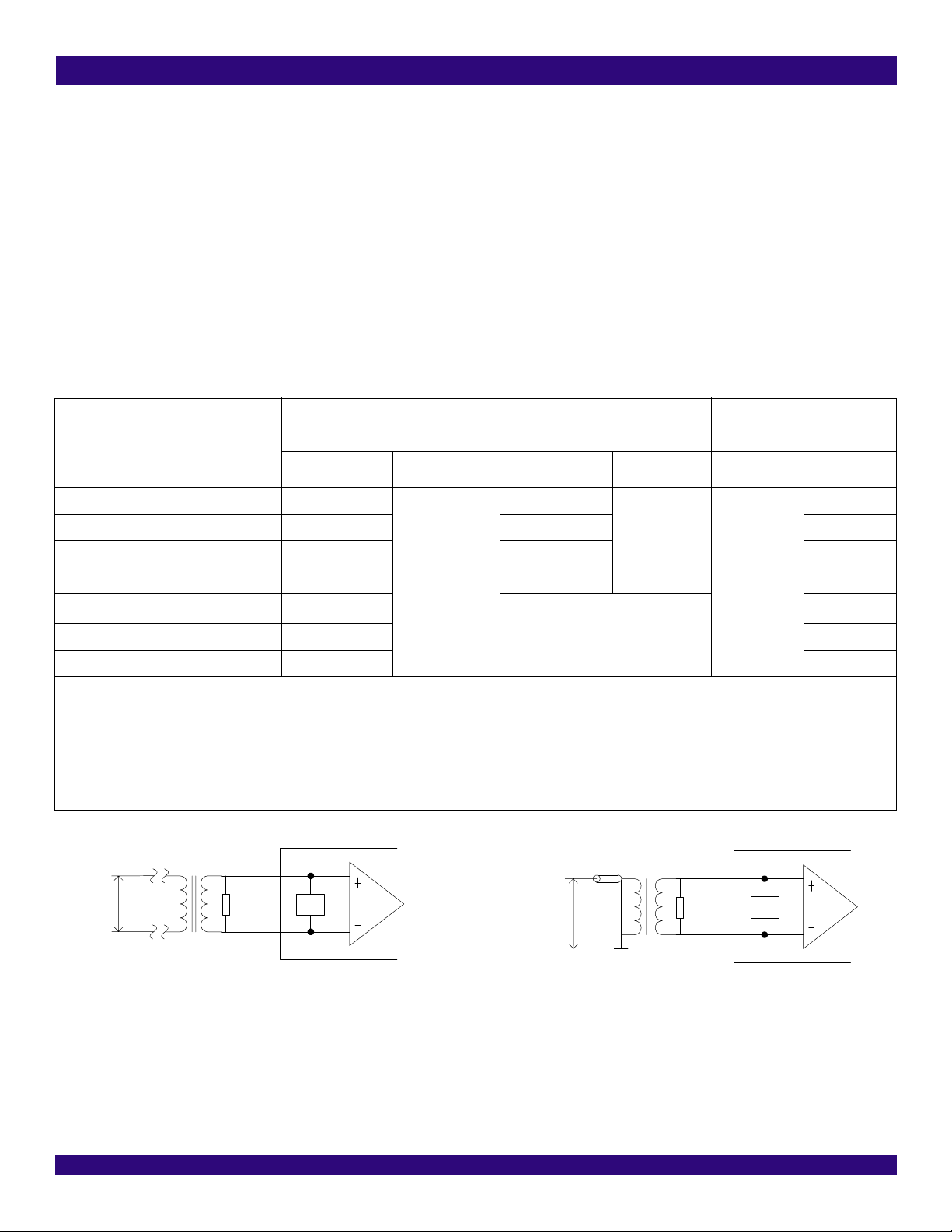
IDT82P2828 28(+1) CHANNEL HIGH-DENSITY T1/E1/J1 LINE INTERFACE UNIT
When RIM is low, only External Impedance Matching is supported for
all 29 receivers and the per-channel impedance matching configuration
bits - the R_TERM[2:0] bits (b2~0, RCF0,...) and the R120IN bit (b4,
RCF0,...) - are ignored.
When RIM is high, impedance matching is configured on a perchannel basis. Three kinds of impedance matching are all supported
and selected by the R_TERM[2:0] bits (b2~0, RCF0,...) and the R120IN
bit (b4, RCF0,...). The R_TERM[2] bit (b2, RCF0,...) should be set to
match internal or external impedance. If the R_TERM[2] bit (b2,
RCF0,...) is ‘0’, internal impedance matching is enabled. The R120IN bit
(b4, RCF0,...) should be set to select Partially Internal Impedance
Matching or Fully Internal Impedance Matching. The internal programmable resistor (IM) is determined by the R_TERM[1:0] bits (b1~0,
RCF0,...). If the R_TERM[2] bit (b2, RCF0,...) is ‘1’, external impedance
matching is enabled. The configuration of the R120IN bit (b4, RCF0,...)
and the R_TERM[1:0] bits (b1~0, RCF0,...) is ignored.
A twisted pair cable can be connected with a 1:1 transformer or
without a transformer (transformer-less), while a coaxial cable must be
connected with a 1:1 transformer. Table 2 lists the recommended impedance matching value in different applications. Figure-8 to Figure-10
show the connection for one channel.
The transformer-less connection will offer a termination option with
reduced cost and board space. However, the waveform amplitude is not
standard compliant, and surge protection and common mode depression should be enhanced depending on equipment environment.
Table-2 Impedance Matching Value in Receive Differential Mode
Partially Internal Impedance Matching
Cable Condition
R_TERM[2:0] Rr R_TERM[2:0] Rr
T1 100 Ω twisted pair (with transformer) 000
J1 110 Ω twisted pair (with transformer) 001 001 110 Ω
E1 120 Ω twisted pair (with transformer) 010 010 120 Ω
(R120IN = 0)
1
Fully Internal Impedance Matching
(R120IN = 1)
000
1, 2
(open)
External Impedance Matching
R_TERM[2:0]
3
100 Ω
Rr
E1 75 Ω coaxial (with transformer) 011 011 75 Ω
T1 100 Ω twisted pair (transformer-less
J1 110 Ω twisted pair (transformer-less) 001 110 Ω
E1 120 Ω twisted pair (transformer-less) 010 120 Ω
Note:
1. Partially Internal Impedance Matching and Fully Internal Impedance Matching are not supported when RIM is low.
2. Fully Internal Impedance Matching is not supported in transformer-less applications.
3. When RIM is low, the setting of the R_TERM[2:0] bits is ignored.
4. In transformer-less applications, the device should be protected against overvoltage. There are three important standards for overvoltage protection:
• UL1950 and FCC Part 68;
• Telcordia (Bellcore) GR-1089
• ITU-T K.20, K.21 and K.41
1:1
6.0 Vpp
4
RTIPn
Rr
RRINGn
)
000
IM
Figure-8 Receive Differential Line Interface with Twist-
ed Pair Cable (with transformer)
120 Ω
1XX
100 Ω
(not supported)
1:1
4.74 Vpp
RTIPn
Rr
RRINGn
IM
Figure-9 Receive Differential Line Interface with Coax-
ial Cable (with transformer)
Functional Description 30 January 11, 2007
 Loading...