


Integrated Device Technology Inc IDT79R3500 Datasheet
IDT79R3500 RISC CPU PROCESSOR RISCore MILITARY AND COMMERCIAL TEMPERATURE RANGES
Integrated Device Technology, Inc.
5.3
© 1992 Integrated Device Technology, Inc. DSC-9054/3
The IDT logo is a registered trademark and RISCore, CEMOS are trademarks of Integrated Device Technology, Inc.
®
RISC CPU PROCESSOR
RISCore
™
IDT79R3500
FEATURES:
• Efficient Pipelining—The CPU’s 5-stage pipeline design
assists in obtaining an execution rate approaching one
instruction per cycle. Pipeline stalls and exceptions are
handled precisely and efficiently.
• On-Chip Cache Control—The IDT79R3500 provides a
high-bandwidth memory interface that handles separate
external Instruction and Data Caches ranging in size from
4 to 256kBs each. Both caches are accessed during a
single CPU cycle. All cache control is on-chip.
• On-Chip Memory Management Unit—A fully-associative,
64-entry Translation Lookaside Buffer (TLB) provides fast
address translation for virtual-to-physical memory mapping of the 4GB virtual address space.
• Dynamically able to switch between Big- and Little- Endian
byte ordering conventions.
• Optimizing Compilers are available for C, FORTRAN,
Pascal, COBOL, Ada, PL/1 and C++.
• 20 through 40MHz clock rates yield up to 32VUPS sustained throughput.
• Supports independent multi-word block refill of both the
instruction and data caches with variable block sizes.
IDT79R3500 PROCESSOR
• Supports concurrent refill and execution of instructions.
• Partial word stores executed as read-modify-write.
• 6 external interrupt inputs, 2 software interrupts, with
single cycle latency to exception handler routine.
• Flexible multiprocessing support on chip with no impact on
uniprocessor designs.
• A single chip integrating the R3000 CPU and R3010 FPA
execution units, using the R3000A pinout.
• Software compatible with R3000, R2000 CPUs and R3010,
R2010 FPAs.
• TLB disable feature allowing a simple memory model for
Embedded Applications.
• Programmable Tag bus width allowing reduced cost cache.
• Hardware Support of Single- and Double-Precision Floating Point Operations that include Add, Subtract, Multiply,
Divide, Comparisons, and Conversions.
• Sustained Floating Point Performance of 11 MFlops single
precision LINPACK and 7.3MFLOPS double precision
• Supports Full Conformance With IEEE 754-1985 Floating
Point Specification
• 64-bit FP operation using sixteen 64-bit data registers
• Military product compliant to MIL-STD 833, class B
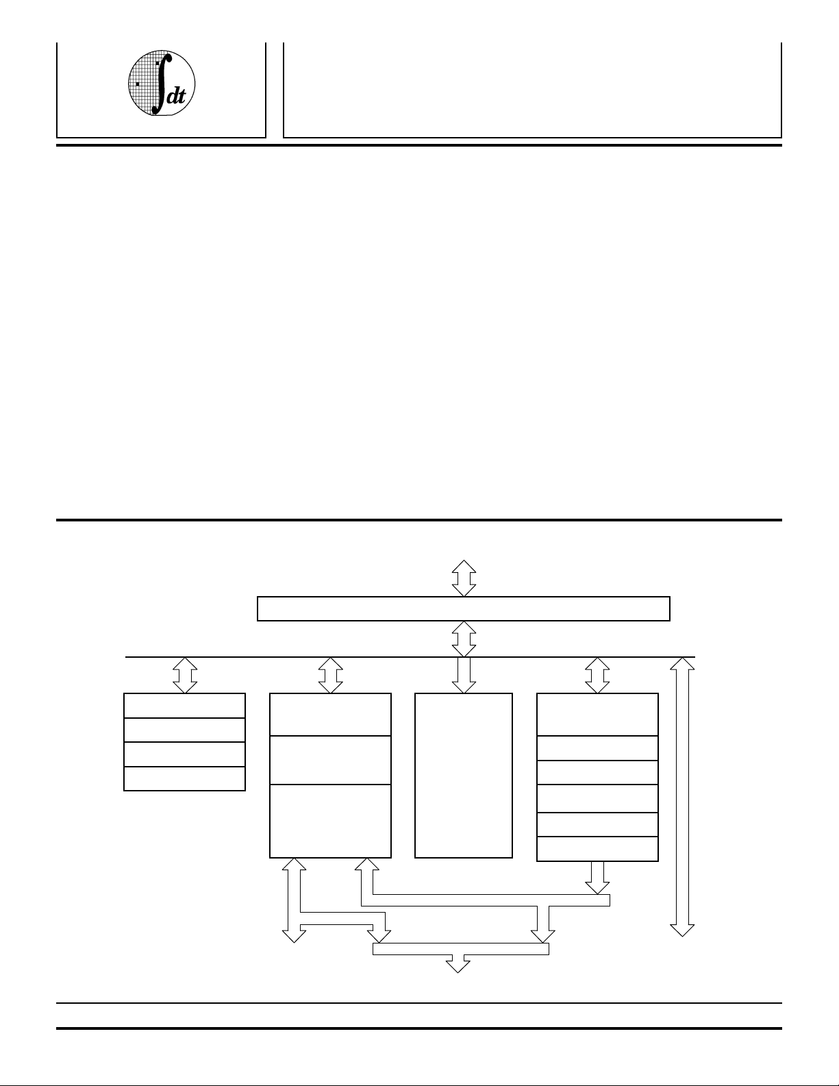
CONTROL
Master Pipeline/Bus Control
FPA
FPA Registers
Exponent Add Unit
FPA Divide Unit
FPA Multiply Unit
(System Control Coprocessor)
CPO
Exception/Control
Registers
Memory
Management
Unit Registers
Translation
Lookaside
Buffer
(64 entries)
TAG (20+4)
Local
Control
Logic
Virtual Page Number/
Virtual Address
ADDRESS (18)
CPU
General Registers
(32x32)
ALU
Shifter
Integer
Multiplier/Divider
Address Adder
PC Increment/Mux
Data (32+4)
2871 drw 01
MILITARY AND COMMERCIAL TEMPERATURE RANGES OCTOBER 1992
IDT79R3500 RISC CPU PROCESSOR RISCore MILITARY AND COMMERCIAL TEMPERATURE RANGES
DESCRIPTION:
The IDT79R3500 RISC Microprocessor consists of three
tightly-coupled processors integrated on a single chip. The
first processor is a full 32-bit CPU based on RISC (Reduced
Instruction Set Computer) principles to achieve a new standard of microprocessor performance. The second processor
is a system control coprocessor, called CP0, containing a
fully-associative 64-entry TLB (Translation Lookaside Buffer),
MMU (Memory Management Unit) and control registers, supporting a 4GB virtual memory subsystem, and a Harvard
Architecture Cache Controller achieving a bandwidth of
320MBs/second using industry standard static RAMs. The
third processor is the Floating Point Accelerator which performs arithmetic operations on values in floating-point representations. This processor fully conforms to the requirements
of ANSI/IEEE Standard 754-1985, “IEEE Standard for Binary
Floating-Point Arithmetic.” In addition, the architecture fully
supports the standard’s recommendations.
The programmer model of this device will be the same as
the programmer model of a system which uses a discrete
IDT79R3000 with the IDT79R3010: 32 integer registers, 16
floating point registers; co-processor 0 registers; floating point
status and control register; RISC integer ALU; Integer Multiply
and Divide ALU; Floating Point Add/Subtract, Multiply, and
Divide ALUs. The device pipeline will be the same as for the
IDT79R3000, as will the co-processor 0 functionality. No new
instructions have been introduced. Pin compatibility extends
to AC and DC characteristics, software execution and initialization mode vector selection.
This data sheet provides an overview of the features and
architecture of the IDT79R3500 CPU, Revision 3.0. A more
detailed description of the operation of the device is incorporated in the R3500 Family Hardware User Manual, and a more
detailed architectural overview is provided in the MIPS RISC
Architecture book, both available from IDT. Documentation
providing details of the software and development environments supporting this processor are also available from IDT.
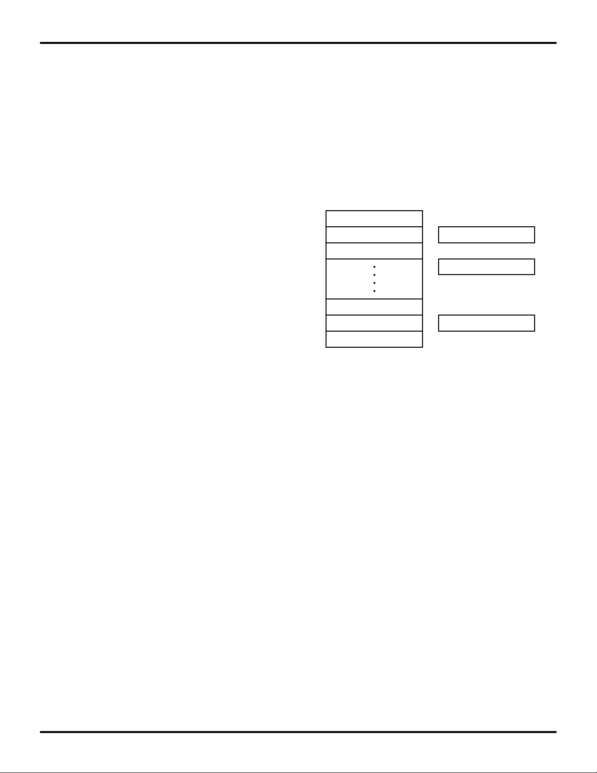
IDT79R3500 CPU Registers
The IDT79R3500 CPU provides 32 general purpose 32bit registers, a 32-bit Program Counter, and two 32-bit registers that hold the results of integer multiply and divide operations. Only two of the 32 general registers have a special
purpose: register r0 is hardwired to the value “0”, which is a
useful constant, and register r31 is used as the link register in
jump-and-link instructions (return address for subroutine calls).
The CPU registers are shown in Figure 2. Note that there
is no Program Status Word (PSW) register shown in this
figure: the functions traditionally provided by a PSW register
are instead provided in the Status and Cause registers incorporated within the System Control Coprocessor (CP0).
FPA REGISTERS
The IDT79R3010A FPA provides 32 general purpose 32bit registers, a Control/Status register, and a Revision Identification register.
Floating-point coprocessor operations reference three types
of registers:
• Floating-Point Control Registers (FCR)
• Floating-Point General Registers (FGR)
• Floating-Point Registers (FPR)
General Purpose Registers
31 0
r0
r1
r2
r29
r30
r31
Figure 2. IDT79R3500 CPU Registers
Floating-Point General Registers (FGR)
There are 32 Floating-Point General Registers (FGR) on
the FPA. They represent directly-addressable 32-bit registers, and can be accessed by Load, Store, or Move Operations.
Floating-Point Registers (FPR)
The 32 FGRs described in the preceding paragraph are
also used to form sixteen 64-bit Floating-Point Registers
(FPR). Pairs of general registers (FGRs), for example FGR0
and FGR1 (Figure 3) are physically combined to form a single
64-bit FPR. The FPRs hold a value in either single- or doubleprecision floating-point format. Double-precision format FPRs
are formed from two adjacent FGRs.
Floating-Point Control Registers (FCR)
There are 2 Floating-Point Control Registers (FCR) on the
FPA. They can be accessed only by Move operations and
include the following:
• Control/Status register, used to control and monitor exceptions, operating modes, and rounding modes;
• Revision register, containing revision information about
the FPA.
Multiply/Divide Registers
31 0
HI
31 0
LO
Program Counter
31 0
PC
2871 drw 02
IDT79R3500 RISC CPU PROCESSOR RISCore MILITARY AND COMMERCIAL TEMPERATURE RANGES
General Purpose Registers
63 32 31 0
FGR1
FGR3
FGR5
FGR27
FGR29
FGR31
(FGR/FPR)
FGR0
FGR2
FGR4
FGR26
FGR28
FGR30
Figure 3. FPA Registers
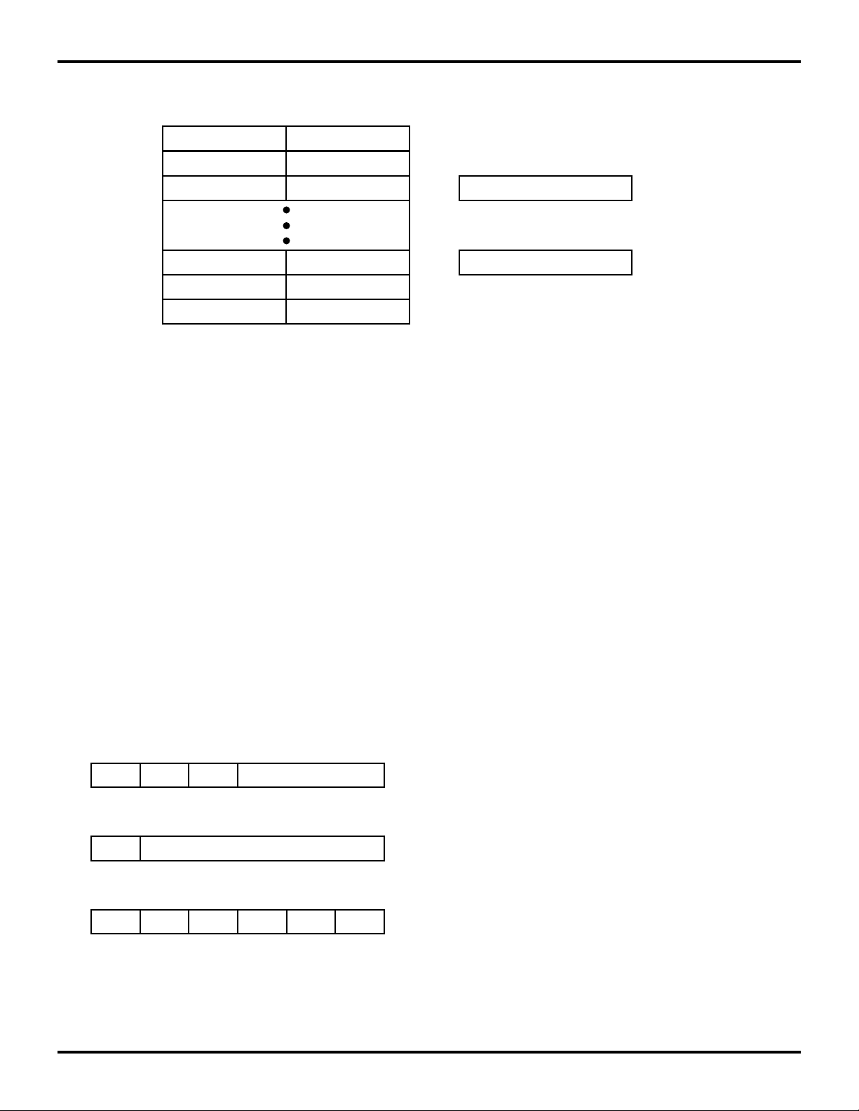
Instruction Set Overview
All IDT79R3500 instructions are 32 bits long, and there
are only three instruction formats. This approach simplifies
instruction decoding, thus minimizing instruction execution
time. The IDT79R3500 processor initiates a new instruction
on every run cycle, and is able to complete an instruction on
almost every clock cycle. The only exceptions are the Load
instructions and Branch instructions, which each have a single
cycle of latency associated with their execution. Note, however, that in the majority of cases the compilers are able to fill
these latency cycles with useful instructions which do not
require the result of the previous instruction. This effectively
eliminates these latency effects.
The actual instruction set of the CPU was determined after
extensive simulations to determine which instructions should
be implemented in hardware, and which operations are best
synthesized in software from other basic instructions. This
methodology resulted in the IDT79R3500 having the highest
performance of any available microprocessor.
I-Type (Immediate)
31 25 20 1526 21 16 0
op rs rt immediate
J-Type (Jump)
31 2526 0
op target
R-Type (Register)
31 25 20 1526 21 16 6
op rs rt
Figure 4. IDT79R3500 Instruction Formats
1011 5 0
rd re funct
2871 drw 04
Control/Status Register
31 0
Exceptions/Enables/Modes
Implementation/Revision
31 0
Register
2871 drw 03
The IDT79R3500 instruction set can be divided into the
following groups:
• Load/Store instructions move data between memory and
general registers. They are all I-type instructions, since the
only addressing mode supported is base register plus 16bit, signed immediate offset.
The Load instruction has a single cycle of latency, which
means that the data being loaded is not available to the
instruction immediately after the load instruction. The
compiler will fill this delay slot with either an instruction
which is not dependent on the loaded data, or with a NOP
instruction. There is no latency associated with the store
instruction.
Loads and Stores can be performed on byte, half-word,
word, or unaligned word data (32-bit data not aligned on a
modulo-4 address). The CPU cache is constructed as a
write-through cache.
• Computational instructions perform arithmetic, logical
and shift operations on values in registers. They occur in
both R-type (both operands and the result are registers)
and I-type (one operand is a 16-bit immediate) formats. FP
computational instructions perform arithmetic operations
on floating point values in the FPA registers. Note that
computational instructions are three operand instructions;
that is, the result of the operation can be stored into a
different register than either of the two operands. This
means that operands need not be overwritten by arithmetic
operations. This results in a more efficient use of the large
register set.
• Conversion instructions perform conversion operations
on the floating point values in the FPA registers.
• Compare intructions perform comparisons of the contents
of FPA registers and set a condition bit based on the
results. The result of the compare operations is tied
directly to Cp Cond (1) for software testing.
• Jump and Branch instructions change the control flow of
a program. Jumps are always to a paged absolute address
formed by combining a 26-bit target with four bits of the
Program counter (J-type format, for subroutine calls), or
32-bit register byte addresses (R-type, for returns and

IDT79R3500 RISC CPU PROCESSOR RISCore MILITARY AND COMMERCIAL TEMPERATURE RANGES
OP
Description Description
Load/Store Instructions
LB Load Byte
LBU Load Byte Unsigned
LH Load Halfword
LHU Load Halfword Unsigned
LW Load Word
LWL Load Word Left
LWR Load Word Right
SB Store Byte
SH Store Halfword
SW Store Word
SWL Store Word Left
SWR Store Word Right
FPA Load/Store/Move Instructions
LWC1 Load Word to FPA
SWC1 Store Word from FPA
MTC1 Move Word to FPA
MFC1 Move Word from FPA
CTC1 Move Control word to FPA
CFC1 Move Control word from FPA
Arithmetlc Instructions
(ALU Immediate)
ADDI Add Immediate
ADDIU Add Immediate Unsigned
SLTI Set on Less Than Immediate
SLTIU Set on Less Than Immediate
Unsigned
ANDI AND Immediate
ORI OR Immediate
XORI Exclusive OR Immediate
LUI Load Upper Immediate
Arithmetic Instructions
(3-operand, register-type)
ADD Add
ADDU Add Unsigned
SUB Subtract
SUBU Subtract Unsigned
SLT Set on Less Than
SLTU Set on Less Than Unsigned
AND AND
OR OR
XOR Exclusive OR
NOR NOR
FPA Computational Instructions
ADD.fmt Floating point Add
SUB.fmt Floating point Subtract
MUL.fmt Floating point Multiply
DlV.fmt Floating point Divide
ABS.fmt Floating-point Absolute value
MOV.fmt Floating point Move
NEG.fmt Floating point Negate
FPA Compare Instructions
C.cond.fmt Floating-point Compare
Shift Instructions
SLL Shift Left Logical
SRL Shift Right Logical
OP
SRA Shift Right Arithmetic
SLLV Shift Left Logical Variable
SRLV Shift Right Logical Variable
SRAV Shift Right Arithmetic Variable
CVT.S.fmt Floating point Convert to Single FP
CVT.D.fmt Floating point Convert to Double FP
CVT.W.fmt Floating point Convert to fixed point
MULT Multiply
MULTU Multiply Unsigned
DIV Divide
DIVU Divide Unsigned
MFHI Move From HI
MTHI Move To HI
MFLO Move From LO
MTLO Move To LO
J Jump
JAL Jump and Link
JR Jump to Register
JALR Jump and Link Register
BEQ Branch on Equal
BNE Branch on Not Equal
BLEZ Branch on Less than or Equal to Zero
BGTZ Branch on Greater Than Zero
BLTZ Branch on Less Than Zero
BGEZ Branch on Greater than or
BLTZAL Branch on Less Than Zero and Link
BGEZAL Branch on Greater than or Equal to
SYSCALL System Call
BREAK Break
LWCZ Load Word from Coprocessor
SWCZ Store Word to Coprocessor
MTCZ Move To Coprocessor
MFCZ Move From Coprocessor
CTCZ Move Control to Coprocessor
CFCZ Move Control From Coprocessor
COPZ Coprocessor Operation
BCZT Branch on Coprocessor z True
BCZF Branch on Coprocessor z False
MTC0 Move To CP0
MFC0 Move From CP0
TLBR Read indexed TLB entry
TLBWI Write Indexed TLB entry
TLBWR Write Random TLB entry
TLBP Probe TLB for matching entry
RFE Restore From Exception
IDT79R3500 Instruction Summary
Shift Instructions (Cont.)
FPA Conversion Instructions
MultIply/Divide Instructions
Jump and Branch Instructions
Equal to Zero
Zero and Link
Special Instructions
Coprocessor Instructions
System Control Coprocessor
(CPO) Instructions
2871 tbl 01
IDT79R3500 RISC CPU PROCESSOR RISCore MILITARY AND COMMERCIAL TEMPERATURE RANGES
dispatches). Branches have 16-bit offsets relative to the
program counter (I-type). Jump and Link instructions save
a return address in Register 31. The R3500 instruction set
features a number of branch conditions. Included is the
ability to compare a register to zero and branch, and also
the ability to branch based on a comparison between two
registers. Thus, net performance is increased since software does not have to perform arithmetic instructions prior
to the branch to set up the branch conditions.
• Coprocessor instructions perform operations in the
coprocessors. Coprocessor Loads and Stores are I-type.
• Coprocessor 0 instructions perform operations on the Sys-
tem Control Coprocessor (CP0) registers to manipulate
the memory management and exception handling facilities
of the processor.
• Special instructions perform a variety of tasks, including
movement of data between special and general registers,
system calls, and breakpoint. They are always R-type.
Table 1 lists the instruction set of the IDT79R3500 processor.
IDT79R3500 System Control Coprocessor (CP0)
The IDT79R3500 can operate with up to four tightlycoupled coprocessors (designated CP0 through CP3). The
System Control Coprocessor (or CP0), is incorporated on the
IDT79R3500 chip and supports the virtual memory system
and exception handling functions of the IDT79R3500. The
virtual memory system is implemented using a Translation
Lookaside Buffer and a group of programmable registers as
shown in Figure 5.
SYSTEM CONTROL COPROCESSOR (CP0)
INSTRUCTIONS
Register Description
EntryHi High half of a TLB entry
EntryLo Low half of a TLB entry
Index Programmable pointer into TLB array
Random Pseudo-random pointer into TLB array
Status Mode, interrupt enables, and diagnostic status info
Cause Indicates nature of last exception
EPC Exception Program Counter
Context Pointer into kernel’s virtual Page Table Entry array
BadVA Most recent bad virtual address
PRId Processor revision identification (Read only)
2871 tbl 02
STATUS CAUSE EPC
ENTRYHI ENTRYLO
63
TLB
INDEX
RANDOM
CONTEXT
System Control Coprocessor (CP0) Registers
The CP0 registers shown in Figure 5 are used to control
the memory management and exception handling capabilities
of the IDT79R3500. Table 2 provides a brief description of
each register.
8
7
NOT ACCESSED
0
BY RANDOM
Used with Virtual Memory System
Used with Exception Processing
Figure 5. The System Coprocessor Registers
BADVA
2871 drw 05