


Integrated Device Technology Inc IDT75FCT646SOB, IDT75FCT646SO, IDT75FCT646PB, IDT75FCT646P, IDT75FCT646LB Datasheet
...
Integrated Device Technology, Inc.
MILITARY AND COMMERCIAL TEMPERATURE RANGES MAY 1992
1992 Integrated Device Technology, Inc. 7.18 DSC-4626/2
The IDT logo is a registered trademark of Integrated Device Technology, Inc.
FAST is a registered trademark of National Semiconductor Co.
IDT54/74FCT646
IDT54/74FCT646A
IDT54/74FCT646C
FEATURES:
• IDT54/74FCT646 equivalent to FAST speed;
• IDT54/74FCT646A 30% faster than FAST
• IDT54/74FCT646C 40% faster than FAST
• Independent registers for A and B buses
• Multiplexed real-time and stored data
•IOL = 64mA (commercial) and 48mA (military)
• CMOS power levels (1mW typical static)
• TTL input and output level compatible
• CMOS output level compatible
• Available in 24-pin (300 mil) CERDIP, plastic DIP, SOIC,
CERPACK and 28-pin LCC
• Product available in Radiation Tolerant and Radiation
Enhanced Versions
• Military product compliant to MIL-STD-883, Class B
DESCRIPTION:
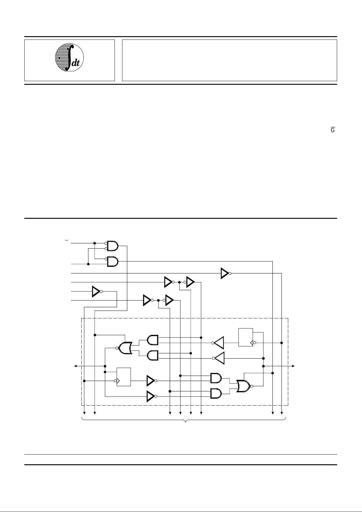
The IDT54/74FCT646/A/C consists of a bus transceiver
with 3-state D-type flip-flops and control circuitry arranged for
multiplexed transmission of data directly from the data bus or
from the internal storage registers.
The IDT54/74FCT646/A/C utilizes the enable control (G)
and direction (DIR) pins to control the transceiver functions.
SAB and SBA control pins are provided to select either real
time or stored data transfer. The circuitry used for select
control will eliminate the typical decoding glitch that occurs in
a multiplexer during the transition between stored and realtime data. A LOW input level selects real-time data and a
HIGH selects stored data.
Data on the A or B data bus or both can be stored in the
internal D flip flops by LOW-to-HIGH transitions at the
appropriate clock pins (CPAB or CPBA) regardless of the
select or enable control pins.
FAST CMOS OCTAL
TRANSCEIVER/REGISTER
FUNCTIONAL BLOCK DIAGRAM
2536 drw 01
1D
C1
A REG
A
1
1D
C1
B REG
B1
TO 7 OTHER CHANNELS
1 OF 8 CHANNELS
SAB
CPBA
CPAB
SBA
DIR
G
1
7.18 2
IDT54/74FCT646/A/C
FAST CMOS OCTAL TRANSCEIVER/REGISTER MILITARY AND COMMERCIAL TEMPERATURE RANGES
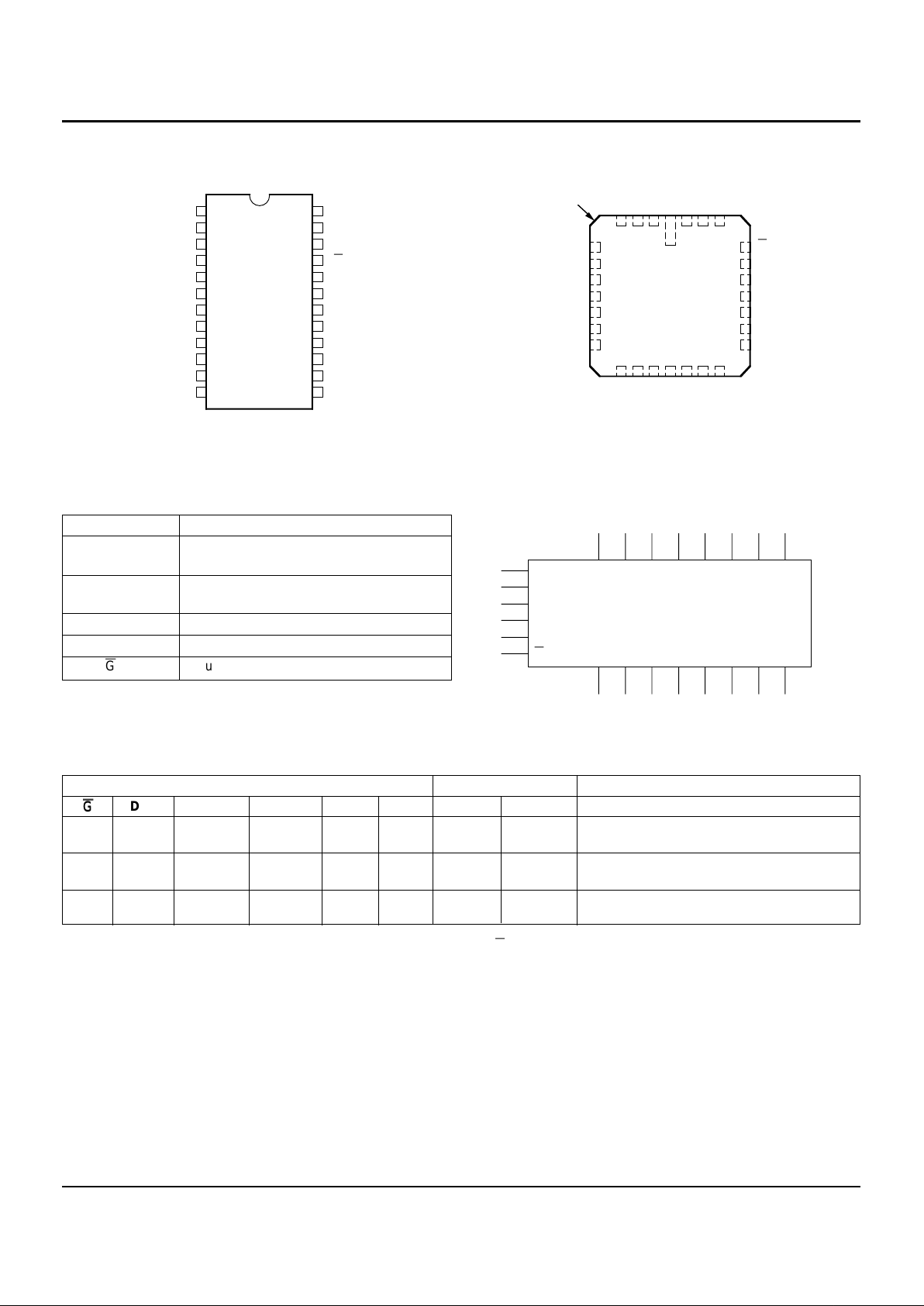
PIN CONFIGURATIONS
LCC
TOP VIEW
DIP/SOIC/CERPACK
TOP VIEW
FUNCTION TABLE
(2)
Inputs Data I/O
(1)
Operation or Function
G
G
DIR CPAB CPBA SAB SBA A
1–A8 B1–B8 IDT54/74FCT646
H X H or L H or L X X Input Input Isolation
HX ↑↑X X Store A and B Data
L L X X X L Output Input Real-Time B Data to A Bus
L L X H or L X H Stored B Data to A Bus
L H X X L X Input Output Real-Time A Data to B Bus
L H H or L X H X Stored A Data to B Bus
NOTES: 2536 tbl 02
1. The data output functions may be enabled or disabled by various signals at the G or DIR inputs. Data input functions are always enabled, i.e., data at
the bus pins will be stored on every LOW-to-HIGH transition on the clock inputs.
2. H = HIGH, L = LOW, X = Don’t Care, ↑ = LOW-to-HIGH Transition.
PIN DESCRIPTION
Pin Names Description
A
1–A8 Data Register A Inputs
Data Register B Outputs
B
1–B8 Data Register B Inputs
Data Register A Outputs
CPAB, CPBA Clock Pulse Inputs
SAB, SBA Output Data Source Select Inputs
DIR,
G
Output Enable Inputs
2536 tbl 01
LOGIC SYMBOL
5
6
7
8
9
10
11
12
GND
A
1
A
2
A
3
1
2
3
4
24
23
22
21
20
19
18
17
Vcc
16
15
14
13
CPAB
P24-1,
D24-1,
S024-2
&
E24-1
B
1
A
4
A
5
A
6
SAB
DIR
A
7
A
8
CPBA
SBA
G
B
2
B
3
B
4
B
5
B
6
B
7
B
8
2536 drw 06
CPAB
SAB
DIR
CPBA
SBA
G
A1B1A2B2A3B3A4B4A5B5A6B6A7B7A8
B8
5
6
7
8
9
10
11
L28-1
25
24
23
22
21
20
19
INDEX
2536 drw 02
B
1
G
B
2
B
3
B
4
B
5
NC
A
1
A
2
A
3
A
4
A
5
A
6
NC
Vcc
CPAB
SAB
DIR
CPBA
SBA
NC
GND
A
7A8
B8B7B
6
NC
12 13 14 15 16 17 18
432128 27 26
IDT54/74FCT646/A/C
FAST CMOS OCTAL TRANSCEIVER/REGISTER MILITARY AND COMMERCIAL TEMPERATURE RANGES
7.18 3
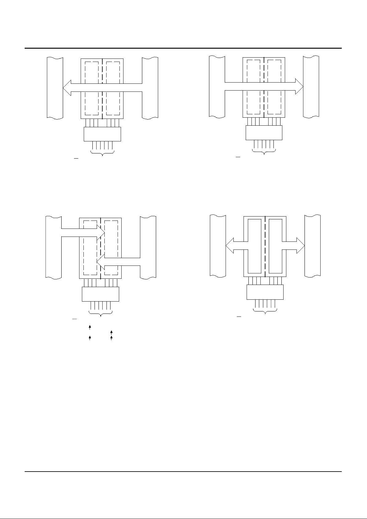
BUS
A
BUS
B
DIRLGLCPABXCPBAXSABXSBA
L
2536 drw 03
BUS
A
BUS
B
DIRHGLCPABXCPBAXSABLSBA
X
BUS
A
BUS
B
DIR
H
L
X
G
L
L
H
CPABXCPBAXSAB
X
X
X
SBA
X
X
X
2536 drw 04
BUS
A
BUS
B
DIR
L
H
G
L
L
CPAB
X
H or L
CPBA
H or L
X
SAB
X
H
SBA
H
X
(1)
STORAGE FROM
A AND/OR B
REAL–TIME TRANSFER
BUS B TO BUS A
REAL–TIME TRANSFER
BUS A TO BUS B
TRANSFER STORED
DATA TO A AND/OR B
NOTE:
1. Cannot transfer data to A bus and B bus simultaneously.