

IDT IDT74GTLP16612 User Manual
查询IDT74GTLP16612供应商
IDT74GTLP16612
CMOS 18-BIT TTL/GTLP UNIVERSAL BUS TRANSCEIVER
INDUSTRIAL TEMPERATURE RANGE
CMOS 18-BIT TTL/GTLP
UNIVERSAL BUS
TRANSCEIVER
FEA TURES:
• Bidirectional interface between GTLP and TTL logic levels
• Edge Rate Control Circuit reduces output noise
•VREF pin provides reference voltage for receiver threshold
• CMOS technology for low power dissipation
• Special PVT Compensation circuitry to provide consistent performance over variations of process, supply voltage, and temperature
• 5V tolerant inputs and outputs on A-Port
• Bus-Hold to eliminate the need for external pull-up resistors for
unused inputs to A-Port
• Power up/down high-impedance
• TTL-compatible Driver and Control inputs
• High Output source/sink ±32mA on A-Port pins
• Flow-through architecture optimizes system layout
• D-type latch and flip-flop architecture for data flow in clocked,
transparent, or latched mode
• Open drain on GTLP to support wired OR connection
• Available in SSOP and TSSOP packages
IDT74GTLP16612
PRELIMINARY
DESCRIPTION:
The GTLP16612 is an 18-bit universal bus transceiver. It provides
signal level translation, from TTL to GTLP, for applications requiring a highspeed interface between cards operating at TTL logic levels and backplanes operating at GTLP logic levels. GTLP provides reduced output
swing (<1V), reduced input threshold levels, and output edge-rate control
to minimize signal setting times. The GTLP16612 is a derivative of the Gunning Transceiver Logic (GTL) JEDEC standard JESD8-3 and incorporates
internal edge-rate control, which is process, voltage, and temperature
(PVT) compensated.
GTLP output low voltage is less than 0.5V. The output high is 1.5V, and
the receiver threshold is 1V.
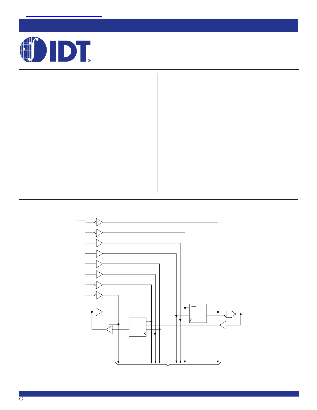
FUNCTIONAL BLOCK DIAGRAM
1
OEAB
56
CEAB
55
CLKAB
2
LEAB
28
LEBA
30
CLKBA
29
CEBA
27
OEBA
3
A1
CLK
ONE OF 18 CHANNELS
CE
1D
C1
CE
1D
C1
CLK
GTLP
54
B1
The IDT logo is a registered trademark of Integrated Device Technology, Inc.
INDUSTRIAL TEMPERATURE RANGE
1999 Integrated Device Technology, Inc. DSC-5477/1c
TO 17 OTHER CHANNELS
OCTOBER 1999
1
IDT74GTLP16612
CMOS 18-BIT TTL/GTLP UNIVERSAL BUS TRANSCEIVER
INDUSTRIAL TEMPERATURE RANGE
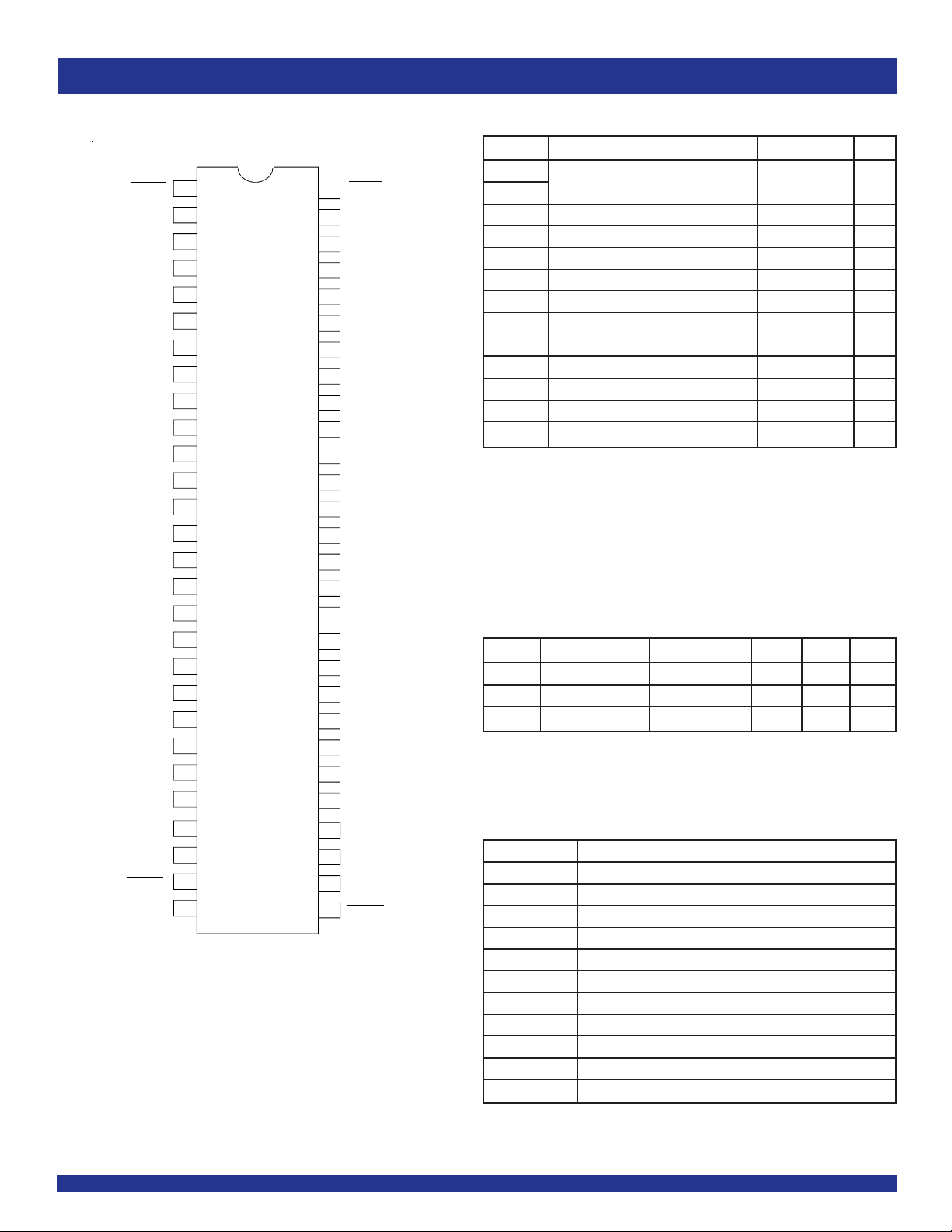
PIN CONFIGURATION
OEAB
LEAB
A
GND
A
A3
V
CC (3.3V)
A4
A5
A6
GND
A7
A8
A9
A10
A11
A12
GND
A13
A14
A15
VCC (3.3V )
A16
A17
GND
A18
OEBA
LEBA
1
2
Q
2
3
4
5
6
7
8
9
10
11
12
13
14
15
16
17
18
19
20
21
22
23
24
25
26
27
28
SSOP/ TSSOP
TOP VIEW
561
55
54
53
52
51
50
49
48
47
46
45
44
43
42
41
40
39
38
37
36
35
34
33
32
31
30
29
CEAB
CLKAB
1
B
GND
2
B
B3
CCQ (5V)
V
B4
B5
B6
GND
B7
B8
B9
B10
B11
B12
GND
B13
B14
B15
V
REF
B16
17
B
GND
B18
CLKBA
CEBA
ABSOLUTE MAXIMUM RATINGS
Symbol Rating Max. Unit
V
CC Supply Voltage –0.5 to +7 V
VCCQ
VI DC Input Voltage –0.5 to +7 V
VO DC Output Voltage, 3-State –0.5 to +7 V
VO DC Output Voltage, Active –0.5 to VCC + 0.5 V
IOL DC Output Sink Current into A-port 6 4 mA
IOH DC Output Source Current from A-port –64 mA
OL DC Output Sink Current into B-port 8 0 mA
I
(in the LOW state)
IIK DC Input Diode Current VI < 0V –50 mA
IOK DC Output Diode Current VO < 0V –5 0 mA
IOK DC Output Diode Current VO > VCC +50 mA
TSTG Storage Temperature –65 to +150 °C
NOTES:
1. Stresses greater than those listed under ABSOLUTE MAXIMUM RATINGS may cause
permanent damage to the device. This is a stress rating only and functional operation
of the device at these or any other conditions above those indicated in the operational
sections of this specification is not implied. Exposure to absolute maximum rating
conditions for extended periods may affect reliability.
2. Unused inputs without Bus-Hold must be held HIGH or LOW.
(1,2)
CAPACITANCE (TA = +25°C, f = 1.0MHZ)
Symbol Parameter
CIN Control Pins VI = VCCQ or 0 8 — pF
CI/O A-Port VI = VCCQ or 0 9 — pF
CI/O B-Port VI = VCCQ or 0 6 — pF
NOTES:
1. As applicable to the device type.
2. All typical values are at VCC = 3.3V and VCCQ = 5V.
(1)
Conditions Typ.
(2)
Max. Unit
PIN DESCRIPTION
Pin Names Description
OEAB A-to-B Output Enable (Active LOW)
OEBA B-to-A Output Enable (Active LOW)
CEAB A-to-B Clock Enable (Active LOW)
CEBA B-to-A Clock Enable (Active LOW)
LEAB A-to-B Latch Enable (Transparent HIGH)
LEBA B-to-A Latch Enable (Transparent HIGH)
CLKAB A-to-B Clock Pulse
CLKBA B-to-A Clock Pulse
VREF GTLP Input Reference Voltage
A1 - A18 A-to-B TTL Data Inputs or B-to-A 3-State Outputs
B1 - B18 B-to-A GTLP Data Inputs or A-to-B Open Drain Outputs
NOTE:
1. A-Port pins have Bus-Hold. All other pins are standard input, output, or I/O.
(1)
2

IDT74GTLP16612
CMOS 18-BIT TTL/GTLP UNIVERSAL BUS TRANSCEIVER
INDUSTRIAL TEMPERATURE RANGE
RECOMMENDED OPERATING
CONDITIONS
Symbol Rating Recommended Unit
V
CC Supply Voltage 3.15 to 3.45 V
VCCQ 4.75 to 5.25
VTT Bus Termination Voltage 1.35 to 1.65 V
VI Input Voltage on A-Port and Control Pins 0 to 5.5 V
IOH HIGH Level Output Current (A-Port) -3 2 mA
IOL LOW Level Output Current (A-Port) +32 mA
IOL LOW Level Output Current (B-Port) +34 mA
A Operating Temperature –40 to +85 °C
T
NOTE:
1. Unused inputs without Bus-Hold must be held HIGH or LOW.
(1)
FUNCTIONAL DESCRIPTION:
The GTLP16612 combines a universal transceiver function with a TTL
to GTLP translation. The A-Port and control pins operate at LVTTL or 5V
TTL levels while the B-Port operates at GTLP levels. The transceiver logic
includes D-type latches and D-type flip-flops to allow data flow in transparent,
latched, and clock mode.
FUNCTION TABLE
(1,2)
Inputs Outputs Mode
CEAB OEAB LEAB CLKAB Ax Bx
X H X X X Z Latched
LLLHXB
LLL LXB
(3)
0
(4)
0
X L H X L L Transparent
XLH XHH
LLL ↑ L L Clocked storage
LLL ↑ H H of A data
HLLXXB
NOTES:
1. H = HIGH Voltage Level
L = LOW Voltage Level
X = Don’t Care
↑ = LOW-to-HIGH Transition
2. A-to-B data flow is shown. B-to-A data flow is similar, but uses OEBA, LEBA, CLKBA, and CEBA.
3. Output level before the indicated steady-state input conditions were established, provided that CLKAB was HIGH before LEAB went LOW.
4. Output level before the indicated steady-state input conditions were established.
(4)
0
storage
of A data
Clock Inhibit
3
 Loading...