

Integrated Device Technology Inc IDT74FST16163212PV, IDT74FST16163212PF, IDT74FST16163212PA Datasheet
Integrated Device Technology, Inc.
The IDT logo is a registered trademark of Integrated Device Technology, Inc.
FEATURES:
• Bus switches provide zero delay paths
• Extended commercial range of –40°C to +85°C
• Low switch on-resistance:
FST163xxx – 4Ω
• TTL-compatible input and output levels
• ESD > 2000V per MIL-STD-883, Method 3015;
> 200V using machine model (C = 200pF, R = 0)
• Available in SSOP, TSSOP and TVSOP
COMMERCIAL TEMPERATURE RANGE SEPTEMBER 1996
1996 Integrated Device Technology, Inc. DSC-3508/-
1
IDT74FST163212
ADVANCE INFORMATION
24-BIT BUS EXCHANGE
SWITCH
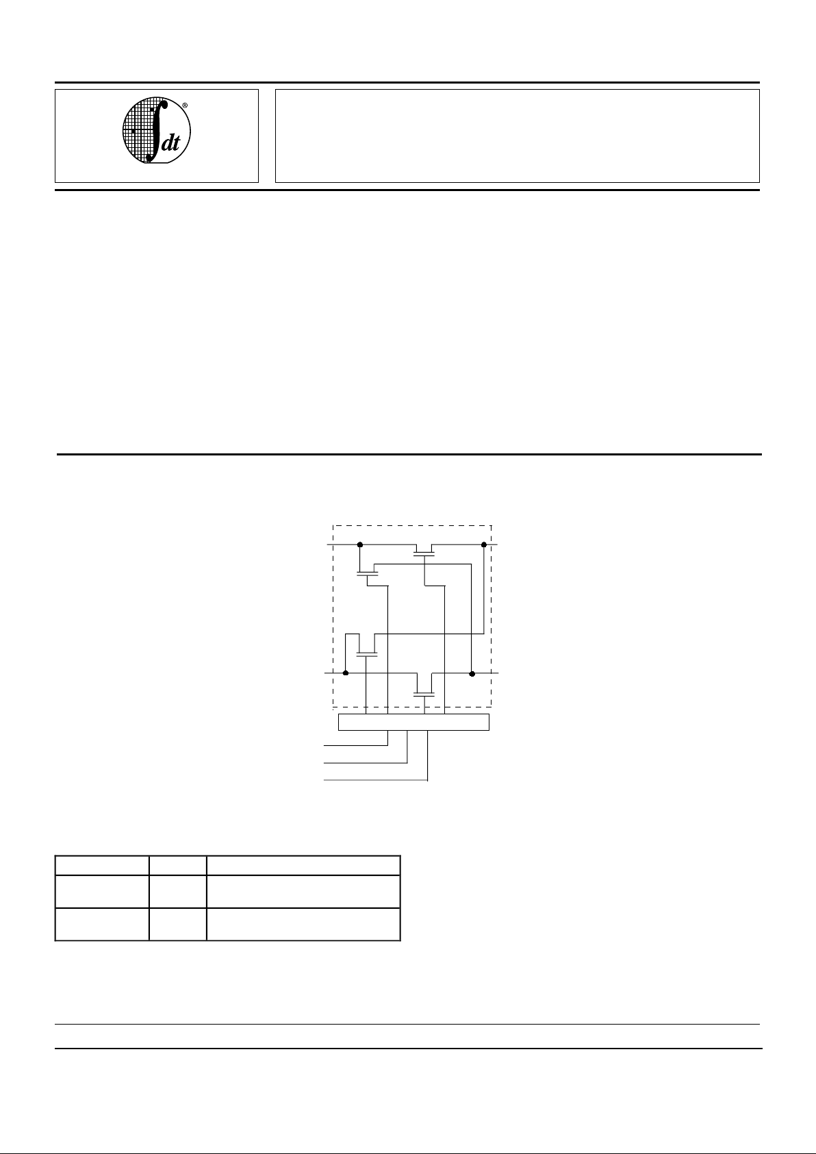
or source capability. Thus they generate little or no noise of
their own while providing a low resistance path for an external
driver. These devices connect input and output ports through
an n-channel FET. When the gate-to-source junction of this
FET is adequately forward-biased the device conducts and
the resistance between input and output ports is small. Without adequate bias on the gate-to-source junction of the FET,
the FET is turned off, therefore with no VCC applied, the device
has hot insertion capability.
The low on-resistance and simplicity of the connection
between input and output ports reduces the delay in this path
to close to zero.
The FST163212 provides four 12-bit TTL- compatible ports
that support 2 way bus exchange. The S
0-2 pins control the
bus exchange and switch enable functions.
PIN DESCRIPTION
3508 tbl 01
FUNCTIONAL BLOCK DIAGRAM
1A1
S0
S1
1
B1
1 of 12 Channels
Flow Control
1B2
1
A2
S2
3508 drw 01
DESCRIPTION:
The FST163212 belongs to IDT's family of Bus switches.
Bus switch devices perform the function of connecting or
isolating two ports without providing any inherent current sink
Pin Names I/O Description
A
1, A2
B
1, B2
I/O Buses A
1, A2
, B
1, B2
S
0-2
I Control Pins for Mux and Switch
Enable Functions
2
IDT74FST163212
24-BIT BUS EXCHANGE SWITCH COMMERCIAL TEMPERATURE RANGE
ABSOLUTE MAXIMUM RATINGS
(1)
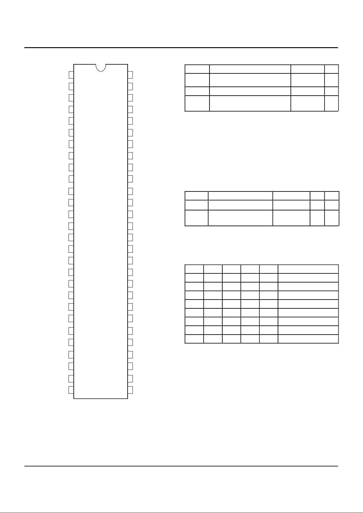
PIN CONFIGURATION
CAPACITANCE
(1)
FUNCTION TABLE
SSOP/
TSSOP/TVSOP
TOP VIEW
5
6
7
8
9
10
1
2
3
4
54
53
52
51
50
49
48
47
46
45
4A2
1
A1
1
A2
2
A1
2
A2
3
A1
3
A2
GND
4A1
1
B1
1
B2
2
B1
2
B2
3
B1
3
B2
4
B1
S1
S2
5A1
11
12
55
56
5A2
4
B2
5
B1
17
18
19
20
21
22
13
14
15
16
42
41
40
39
38
37
36
35
34
33
9A2
6
A2
7
A1
7
A2
6
A1
VCC
8
A1
GND
8A2
9
A1
6
B2
7
B1
7
B2
8
B1
GND
8B2
9
B1
9
B2
5
B2
6
B1
SO56-1
SO56-2
SO56-3
10A1
23
24
43
44
10A2
10
B1
10
B2
25
26
32
31
30
29
11A2
11
A111B1
11
B2
12A1
27
28
12A2
12
B1
12
B2
S0
GND
S2 S1 S0 A1 A2 Function
L L L Z Z Disconnect
LLHB1 ZA1 to B1
LHLB2 ZA1 to B2
LHHZB1 A2 to B1
HLLZB2 A2 to B2
H L H Z Z Disconnect
HHLB1 B2 A1 to B1, A2 to B2
HHHB2 B1 A1 to B2, A2 to B1
3508 drw 02
3508 tbl 04
Symbol Description Max. Unit
VTERM
(2)
Terminal Voltage with Respect
to GND
–0.5 to +7.0 V
TSTG Storage Temperature –65 to +150 °C
IOUT Maximum Continuous Channel
Current
128 mA
3508 tbl 02
NOTES:
1. Stresses greater than those listed under ABSOLUTE MAXIMUM RATINGS may cause permanent damage to the device. This is a stress rating
only and functional operation of the device at these or any other conditions
above those indicated in the operational sections of this specification is not
implied. Exposure to absolute maximum rating condiitions for extended
periods may affect reliability.
2. V
CC, Control and Switch terminals.
Symbol Parameter Conditions
(2)
Typ. Unit
C
IN
Control Input Capacitance 4
pF
C
I/O
Switch Input/Output
Capacitance
Switch Off
pF
3508 tbl 03
NOTES:
1. Capacitance is characterized but not tested
2. T
A = 25°C, f = 1MHz, VIN = 0V, VOUT = 0V
 Loading...