

IDT IDT54FCT833A, IDT54FCT833B, IDT74FCT833A, IDT74FCT833B User Manual
查询IDT54FCT833ADB供应商
Integrated Device Technology, Inc.
FAST CMOS
PARITY BUS
TRANSCEIVER
IDT54/74FCT833A
IDT54/74FCT833B
FEATURES:
• Equivalent to AMD’s Am29833 bipolar parity bus
transceiver in pinout/function, speed and output drive
over full temperature and voltage supply extremes
• High-speed bidirectional bus transceiver for processororganized devices
• IDT54/74FCT833A equivalent to Am29833A speed and
output drive
• IDT54/74FCT833B 30% faster than Am29833A
• Buffered direction and three-state controls
• Error flag with open-drain output
•I
OL = 48mA (commercial) and 32mA (military)
• TTL input and output level compatible
• CMOS output level compatible
• Substantially lower input current levels than AMD’s
bipolar Am29800 series (5µA max.)
• Available in plastic DIP, CERDIP, LCC and SOIC
• Product available in Radiation Tolerant and Radiation
Enhanced versions
• Military product compliant to MIL-STD-883, Class B
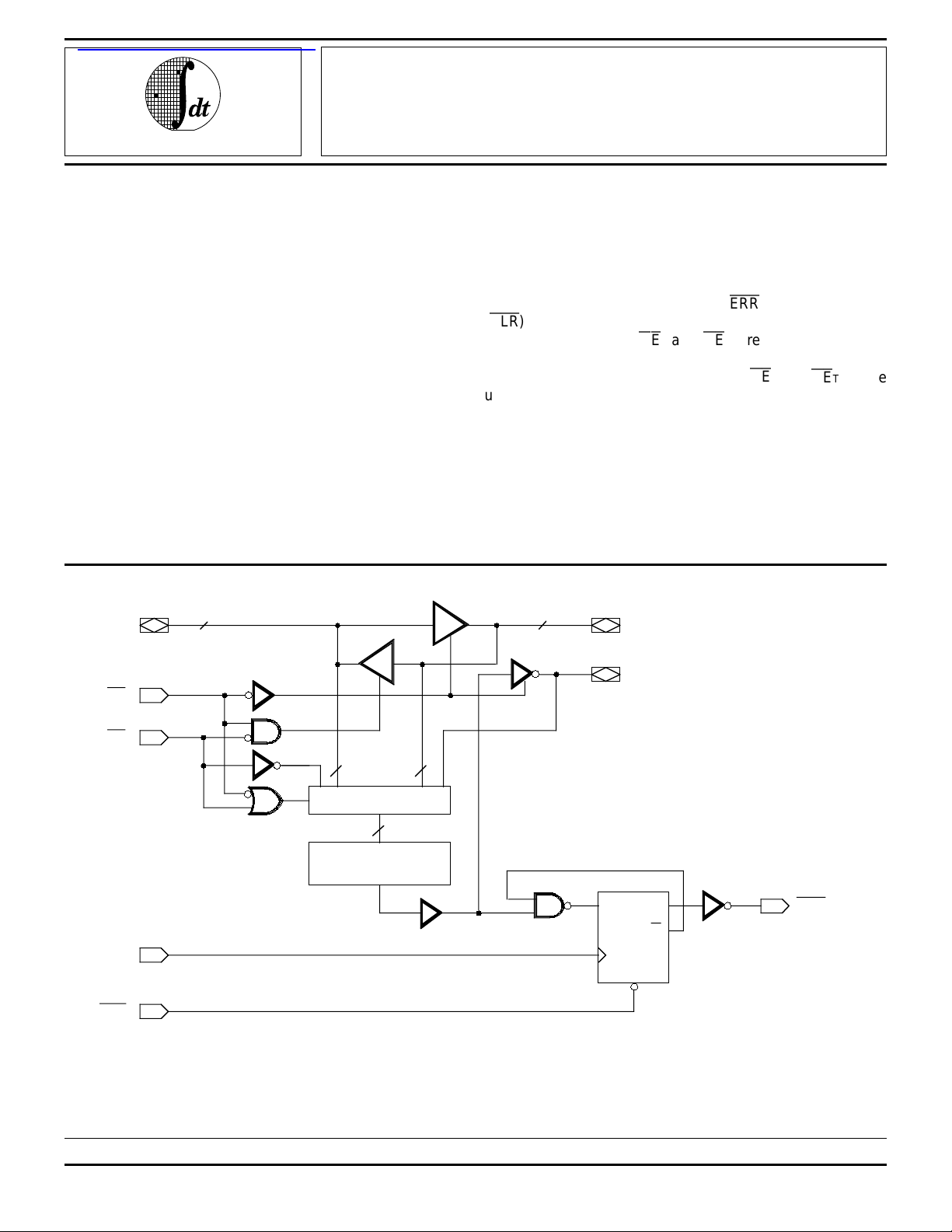
FUNCTIONAL BLOCK DIAGRAM
RI
8
DESCRIPTION:
The IDT54/74FCT833s are high-performance bus
transceivers designed for two-way communications. They
each contain an 8-bit data path from the R (port) to the T (port),
an 8-bit data path from the T (port) to the R (port), and a 9-bit
parity checker/generator. The error flag can be clocked and
stored in a register and read at the
(
CLR
) input is used to clear the error flag register.
The output enables
OE
T and OER are used to force the
port outputs to the high-impedance state so that the device
can drive bus lines directly. In addition,
used to force a parity error by enabling both lines
simultaneously. This transmission of inverted parity gives the
designer more system diagnostic capability. The devices are
specified at 48mA and 32mA output sink current over the
commercial and military temperature ranges, respectively.
T
8
I
ERR
output. The clear
OE
R and OET can be
OE
OE
CLK
CLR
PARITY
T
R
8
S MUX
9-BIT
PARITY TREE
8
9
D
Q
P
Q
CP
CLR
ERR
2557 drw 01
The IDT logo is a registered trademark of Integrated Device Technology, Inc.
MILITARY AND COMMERCIAL TEMPERATURE RANGES MAY 1992
1992 Integrated Device Technology, Inc. 7.21 DSC-4621/2
1

IDT54/74FCT833A/B
FAST CMOS PARITY BUS TRANSCEIVER MILITARY AND COMMERCIAL TEMPERATURE RANGES
PIN CONFIGURATIONS
R
1
R
OE
2
R
0
3
1
R
R
2
R
3
R
4
R
5
R
6
R
7
ERR PARITY
CLR OE
GND
P24-1,
4
D24-1,
5
S024-2
6
7
E24-1
8
9
10
11
12
DIP/SOIC/CERPACK
TOP VIEW
24
Vcc
23
T
22
21
20
19
&
18
17
16
15
14
13
0
T
1
T
2
T
3
T
4
T
5
T
6
T
7
CLK
T
INDEX
R
2
R
3
R
4
NC NC
R
5
R
6
R
7
1
R
432128 27 26
5
6
7
8
9
10
11
12 13 14 15 16 17 18
ERR
NC
OE
R0
L28-1
NC
CLR
GND
LCC
TOP VIEW
Vcc
CLK
T0
T
OE
1
T
25
24
23
22
21
20
19
PARITY
T
2
T
3
T
4
T
5
T
6
T
7
2557 drw 02
PIN DESCRIPTION
Pin Name I/O Description
R I RECEIVE enable input.
OE
I I/O 8-bit RECEIVE data input/output.
R
ERR
CLR
T
I I/O 8-bit TRANSMIT data input/output.
PARITY I/O 1-bit PARITY output.
T I TRANSMIT enable input.
OE
CLK I External clock pulse input for fault register
O Output from fault registers. Register
detection of odd parity fault on rising clock
edge (CLK). A registered
ERR
output
remains LOW until cleared. Open drain
output, requires pull up resistor.
I Clears the fault register output.
flag.
2557 tbl 01
ERROR FLAG OUTPUT FUNCTION TABLE
(1,2)
Internal Output
Inputs To Device Pre-State Output
CLR
CLR
CLK Point “P”
ERR
ERR
n–1
ERR
ERR
Function
H ↑ H H H Sample
H ↑ — L L (1’s
H ↑ L — L Capture)
L — — — H Clear
NOTES: 2557 tbl 02
1.
OE
T is HIGH and OER is LOW.
2. H = HIGH
L = LOW
↑ = LOW-to-HIGH transition of clock
– = Don't Care or Irrelevant
7.21 2

IDT54/74FCT833A/B
FAST CMOS PARITY BUS TRANSCEIVER MILITARY AND COMMERCIAL TEMPERATURE RANGES
FUNCTION TABLE
(2)
Inputs Outputs
T
I Incl Parity
OE
OE
T
OE
R
CLR
OE
CLK RI (∑ or H’s) (∑ of H’s) RI TI Parity
CLR
ERR
ERR
(1)
Function
LHH↑ H (Odd) NA NA H L H Transmit data from R Port
LHH↑ H (Even) NA NA H H L to T Port with parity;
LHH↑ L (Odd) NA NA L L H receiving path is disabled.
LHH↑ L (Even) NA NA L H L
HLH↑ NA H (Odd) H NA NA H Receive data from T Port
HLH↑ NA H (Even) H NA NA L to R Port with parity test
HLH↑ NA L (Odd) L NA NA H resulting in flag:
HLH↑ NA L (Even) L NA NA L transmitting path is disabled.
— — L — — — NA NA NA H Clear the state of error flag
register.
H H H H or L — — Z Z Z * Both transmitting and
H H L — — — Z Z Z H receiving paths are disabled.
HHH↑ H or L (Odd) — Z Z Z H Parity logic defaults to
HHH↑ H or L (Even) — Z Z Z L transmit mode.
LLH↑ H (Odd) NA NA H H L Forced-error checking.
LLH↑ H (Even) NA NA H L H
LLH↑ L (Odd) NA NA L H L
LLH↑ L (Even) NA NA L L H
NOTES: 2557 tbl 03
1. Output state assumes HIGH output pre-state.
2. H = HIGH Z = High Impedance Odd = Odd number of logic one’s
L = LOW NA = Not Applicable Even = Even number of logic one’s
↑ = LOW-to-HIGH transition of clock – = Don’t Care or Irrelevant I = 0, 1, 2, 3, 4, 5, 6, 7
*No change to stored Error State
7.21 3
 Loading...