


Integrated Device Technology Inc IDT74FCT827ATEB, IDT74FCT827ATE, IDT74FCT827ATDB, IDT74FCT827ATD, IDT74FCT827DTD Datasheet
...
IDT54/74FCT827AT/BT/CT/DT, IDT54/74FCT2827AT/BT/CT
HIGH-PERFORMANCE CMOS BUFFERS MILITARY AND COMMERCIAL TEMPERATURE RANGES
FAST CMOS 10-BIT
BUFFERS
Integrated Device Technology, Inc.
FEATURES:
• Common features:
– Low input and output leakage ≤1µA (max.)
– CMOS power levels
– True TTL input and output compatibility
– VOH = 3.3V (typ.)
– VOL = 0.3V (typ.)
– Meets or exceeds JEDEC standard 18 specifications
– Product available in Radiation Tolerant and Radiation
Enhanced versions
– Military product compliant to MIL-STD-883, Class B
and DESC listed (dual marked)
– Available in DIP, SOIC, SSOP, QSOP, CERPACK
and LCC packages
• Features for FCT827T:
– A, B, C and D speed grades
– High drive outputs (-15mA I
• Features for FCT2827T:
– A, B and C speed grades
– Resistor outputs (-15mA IOH, 12mA IOL Com.)
(-12mA IOH, 12mA IOL Mil.)
– Reduced system switching noise
OH, 48mA IOL)
IDT54/74FCT827AT/BT/CT/DT
IDT54/74FCT2827AT/BT/CT
DESCRIPTION:
The FCT827T is built using an advanced dual metal CMOS
technology.
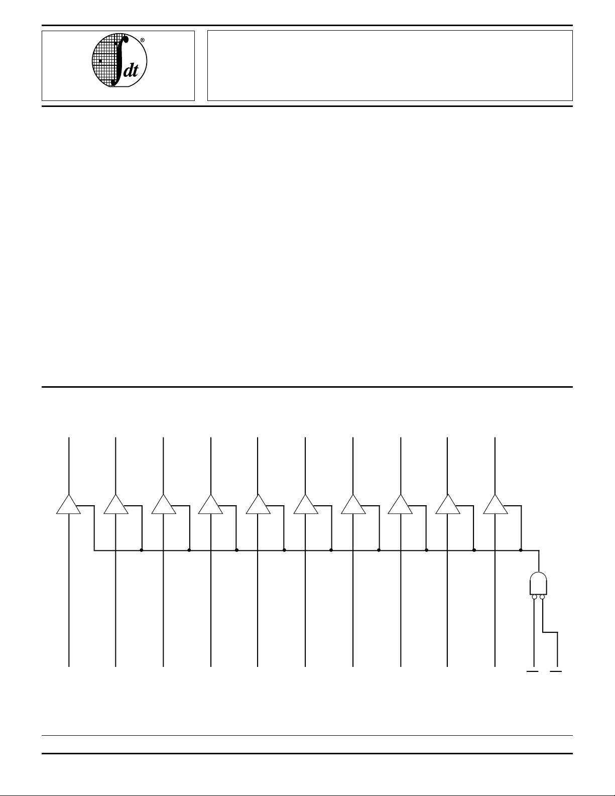
The FCT827T/FCT2827T 10-bit bus drivers provide highperformance bus interface buffering for wide data/address
paths or buses carrying parity. The 10-bit buffers have NANDed output enables for maximum control flexibility.
All of the FCT827T high-performance interface family are
designed for high-capacitance load drive capability, while
providing low-capacitance bus loading at both inputs and
outputs. All inputs have clamp diodes to ground and all outputs
are designed for low-capacitance bus loading in high-impedance state.
The FCT2827T has balanced output drive with current
limiting resistors. This offers low ground bounce, minimal
undershoot and controlled output fall times-reducing the need
for external series terminating resistors. FCT2827T parts are
plug-in replacements for FCT827T parts.
FUNCTIONAL BLOCK DIAGRAM
Y0 Y1 Y2 Y3 Y4 Y5 Y6 Y7 Y8 Y9
D0 D1 D2 D3 D4 D5 D6 D7 D8 D9 OE1 OE2
2573 drw 01
The IDT logo is a registered trademark of Integrated Device Technology, Inc.
MILITARY AND COMMERCIAL TEMPERATURE RANGES AUGUST 1995
1995 Integrated Device Technology, Inc. 6.22 DSC-4217/5
6.22 1
1
IDT54/74FCT827AT/BT/CT/DT, IDT54/74FCT2827AT/BT/CT
HIGH-PERFORMANCE CMOS BUFFERS MILITARY AND COMMERCIAL TEMPERATURE RANGES
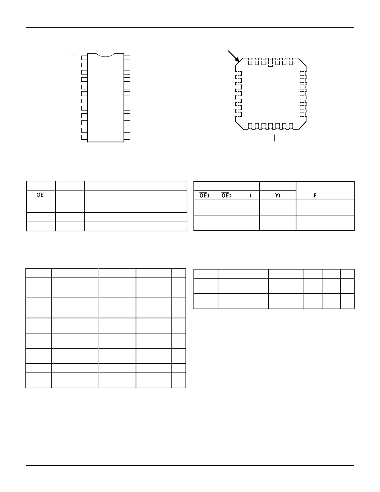
PIN CONFIGURATIONS
1
D
4
1213
8
D
32
1
0
NC
D
OE
1
L28-1
9
D
NC
GND
LCC
TOP VIEW
CC
V
2
OE
1
0
Y
Y
262728
1817161514
Y9Y
25
24
23
22
21
20
19
8
Y
Y
Y
NC
Y
Y
Y
2
3
4
5
6
7
2573 drw 03
24
23
22
21
20
19
18
17
16
15
14
13
VCC1
Y0
Y1
Y2
Y3
Y4
Y5
Y6
Y7
Y8
Y9
OE2GND
OE1
D0
D1
D2
D3
D4
D5
D6
D7
D
D9
2
3
P24-1
4
D24-1
5
SO24-2
6
SO24-7
7
SO24-8
&
8
E24-1
9
10
8
11
12
DIP/SOIC/SSOP/QSOP/CERPACK
TOP VIEW
2573 drw 02
INDEX
D
D3
D
NC
D
D
D
2
5
6
4
7
8
5
9
6
10
7
11
PIN DESCRIPTION
Names I/O Description
OE
I I When both are LOW the outputs are
enabled. When either one or both are
HIGH the outputs are High Z.
DI I 10-bit data input.
YI O 10-bit data output.
2573 tbl 01
(1)
Symbol Rating Commercial Military Unit
(2)
VTERM
VTERM
TA Operating
TBIAS Temperature
TSTG Storage
PT Power Dissipation 0.5 0.5 W
IOUT DC Output
NOTES:
1. Stresses greater than those listed under ABSOLUTE MAXIMUM RATINGS may cause permanent damage to the device. This is a stress rating
only and functional operation of the device at these or any other conditions
above those indicated in the operational sections of this specification is
not implied. Exposure to absolute maximum rating conditions for
extended periods may affect reliability. No terminal voltage may exceed
V
2. Input and V
3. Outputs and I/O terminals only.
Terminal Voltage
–0.5 to +7.0 –0.5 to +7.0 V
with Respect to
GND
(3)
Terminal Voltage
with Respect to
GND
–0.5 to
V
0 to +70 –55 to +125 °C
Temperature
–55 to +125 –65 to +135 °C
Under Bias
–55 to +125 –65 to +150 °C
Temperature
–60 to +120 –60 to +120 mA
Current
CC by +0.5V unless otherwise noted.
CC terminals only.
CC +0.5
–0.5 to
VCC +0.5
V
2573 lnk 03
FUNCTION TABLE
(1)
Inputs Output
OE
1
OE
OE
L
L
H
X
NOTE: 2573 tbl 02
1. H = HIGH, L = LOW, X = Don’t Care, Z = High Impedance
2 DI YI Function
OE
L
L
X
H
L
H
X
X
L
Transparent
H
Z
Three-State
Z
CAPACITANCE (TA = +25°C, f = 1.0MHz)ABSOLUTE MAXIMUM RATINGS
Symbol Parameter
CIN Input
Capacitance
COUT Output
Capacitance
NOTE:
1. This parameter is measured at characterization but not tested.
(1)
Conditions Typ. Max. Unit
VIN = 0V 6 10 pF
VOUT = 0V 8 12 pF
2573 lnk 04
6.22 2
IDT54/74FCT827AT/BT/CT/DT, IDT54/74FCT2827AT/BT/CT
HIGH-PERFORMANCE CMOS BUFFERS MILITARY AND COMMERCIAL TEMPERATURE RANGES
DC ELECTRICAL CHARACTERISTICS OVER OPERATING RANGE
Following Conditions Apply Unless Otherwise Specified:
Commercial: T
Symbol Parameter Test Conditions
A = 0°C to +70°C, VCC = 5.0V ± 5%; Military: TA = –55°C to +125°C, VCC
(1)
VIH Input HIGH Level Guaranteed Logic HIGH Level 2.0 — — V
VIL Input LOW Level Guaranteed Logic LOW Level — — 0.8 V
II H Input HIGH Current
II L Input LOW Current
(4)
(4)
VI = 0.5V — — ±1
VCC = Max. VI = 2.7V — — ±1 µA
IOZH High Impedance Output Current VCC = Max. VO = 2.7V — — ±1 µA
(4)
(4)
VO = 0.5V — — ±1
VCC = Max., VI = VCC (Max.) — — ±1 µA
IOZL (3-State Output pins)
II Input HIGH Current
VIK Clamp Diode Voltage VCC = Min., IIN = –18mA — –0.7 –1.2 V
VH Input Hysteresis — — 200 — mV
ICC Quiescent Power Supply Current VCC = Max., VIN = GND or VCC — 0.01 1 mA
= 5.0V ± 10%
Min. Typ.
(2)
Max. Unit
2573 lnk 05
OUTPUT DRIVE CHARACTERISTICS FOR FCT827T
Symbol Parameter Test Conditions
V
OH
Output HIGH Voltage VCC = Min.
IN
= V
IH
V
or V
IOH = –6mA MIL.
IL
OH
= –8mA COM'L.
I
IOH = –12mA MIL.
OH
= –15mA COM'L.
I
V
OL
I
OS
Output LOW Voltage VCC = Min.
IN
= V
IH
or V
V
IL
Short Circuit Current VCC = Max., VO = GND
I
OL
= 32mA MIL.
OL
= 48mA COM'L.
I
(3)
(1)
Min. Typ.
2.4 3.3 — V
2.0 3.0 — V
— 0.3 0.5 V
–60 –120 –225 mA
(2)
Max. Unit
2573 lnk 06
OUTPUT DRIVE CHARACTERISTICS FOR FCT2827T
Symbol Parameter Test Conditions
I
ODL
I
ODH
V
OH
V
OL
NOTES:
1. For conditions shown as Max. or Min., use appropriate value specified under Electrical Characteristics for the applicable device type.
2. Typical values are at Vcc = 5.0V, +25°C ambient.
3. Not more than one output should be shorted at one time. Duration of the short circuit test should not exceed one second.
4. The test limit for this parameter is ±5µA at T
Output LOW Current VCC = 5V, V
Output HIGH Current VCC = 5V, V
Output HIGH Voltage VCC = Min.
IN
= V
IH
V
or V
Output LOW Voltage VCC = Min.
IN
= V
IH
V
A = –55°C.
or V
IN
= V
IH or VIL, VOUT
IN
= V
IH
IL
IL
or V
IL,VOUT
(1)
(3)
= 1.5V
(3)
= 1.5V
IOH = –12mA MIL.
OH
= –15mA COM'L.
I
Min. Typ.
16 48 — mA
–16 –48 — mA
2.4 3.3 — V
IOL = 12mA — 0.3 0.50 V
(2)
Max. Unit
2573 lnk 07
6.22 3